JP4636384B2 - Tag label making device - Google Patents

Tag label making device Download PDF

Info

Publication number
JP4636384B2
JP4636384B2 JP2006094824A JP2006094824A JP4636384B2 JP 4636384 B2 JP4636384 B2 JP 4636384B2 JP 2006094824 A JP2006094824 A JP 2006094824A JP 2006094824 A JP2006094824 A JP 2006094824A JP 4636384 B2 JP4636384 B2 JP 4636384B2
Authority
JP
Japan
Prior art keywords
tag label
tag
antenna
antenna unit
unit
Prior art date
Legal status (The legal status is an assumption and is not a legal conclusion. Google has not performed a legal analysis and makes no representation as to the accuracy of the status listed.)
Expired - Fee Related
Application number
JP2006094824A
Other languages
Japanese (ja)
Other versions
JP2007272371A (en
Inventor
智康 福井
邦博 安井
勉 大橋
Current Assignee (The listed assignees may be inaccurate. Google has not performed a legal analysis and makes no representation or warranty as to the accuracy of the list.)
Brother Industries Ltd
Original Assignee
Brother Industries Ltd
Priority date (The priority date is an assumption and is not a legal conclusion. Google has not performed a legal analysis and makes no representation as to the accuracy of the date listed.)
Filing date
Publication date
Application filed by Brother Industries Ltd filed Critical Brother Industries Ltd
Priority to JP2006094824A priority Critical patent/JP4636384B2/en
Priority to PCT/JP2007/052983 priority patent/WO2007097288A1/en
Publication of JP2007272371A publication Critical patent/JP2007272371A/en
Application granted granted Critical
Publication of JP4636384B2 publication Critical patent/JP4636384B2/en
Expired - Fee Related legal-status Critical Current
Anticipated expiration legal-status Critical

Links

Images

Description

本発明は、外部と情報の無線通信を行う無線タグ回路素子を備えた無線タグラベルを作成するためのタグラベル作成装置に関する。   The present invention relates to a tag label producing apparatus for producing a RFID label having a RFID circuit element that performs wireless communication of information with the outside.

小型の無線タグとリーダ(読み取り装置)/ライタ(書き込み装置)との間で非接触で情報の読み取り/書き込みを行うRFID(Radio Frequency Identification)システムが知られている。例えばラベル状の無線タグに備えられた無線タグ回路素子は、所定の無線タグ情報を記憶するIC回路部とこのIC回路部に接続されて情報の送受信を行うアンテナとを備えており、無線タグが汚れている場合や見えない位置に配置されている場合であっても、リーダ/ライタ側よりIC回路部の無線タグ情報に対してアクセス(情報の読み取り/書き込み)が可能であり、商品管理や検査工程等の様々な分野において実用が期待されている。   An RFID (Radio Frequency Identification) system that reads / writes information in a non-contact manner between a small wireless tag and a reader (reading device) / writer (writing device) is known. For example, a wireless tag circuit element provided in a label-like wireless tag includes an IC circuit unit that stores predetermined wireless tag information and an antenna that is connected to the IC circuit unit and transmits and receives information. Even if the battery is dirty or placed in an invisible position, the reader / writer can access (read / write information) the RFID tag information in the IC circuit unit, and manage the product. Practical use is expected in various fields such as inspection processes.

例えば、このような無線タグ回路素子に対し情報の書き込みを行うライタとしては、特許文献1に記載のものが知られている。この従来技術では、所定間隔で長方形状のラベル片(ラベル)が貼り付けられた帯状のタグテープ(台紙)がタグテープロール(ロール紙)から繰り出され、搬送路を搬送される際に、各ラベル片に内蔵された無線タグ回路素子のアンテナに対し、装置側で生成した所定の無線タグ情報が送信され、アンテナに接続されたIC回路部(ICチップ)に順次書き込まれるとともに、印字手段(記録ヘッド)によって、上記書き込まれた無線タグ情報に対応した印字情報がRFIDラベル表面に印字されて、無線タグラベルが完成するようになっている。   For example, as a writer for writing information to such a RFID circuit element, the one described in Patent Document 1 is known. In this prior art, when a strip-shaped tag tape (mounting paper) on which rectangular label pieces (labels) are pasted at predetermined intervals is fed out from a tag tape roll (roll paper) and transported through a transport path, Predetermined RFID tag information generated on the device side is transmitted to the antenna of the RFID circuit element built in the label piece, and sequentially written in an IC circuit unit (IC chip) connected to the antenna, and printing means ( Printing information corresponding to the written RFID tag information is printed on the surface of the RFID label by the recording head) to complete the RFID tag label.

特開2004−82432号公報JP 2004-82432 A

一般に、上記従来技術のライタ(書込装置)により無線タグ情報の書き込み及び関連する印字が行われて作成された無線タグラベルは、管理対象(商品等)に対し貼付等により設けられる。そして、リーダ(読み取り装置)により、上記商品等に設けられた無線タグラベルから無線タグ情報を読み取ることで、商品に関する情報を入手して当該商品の管理等が行われる。このように、無線タグラベルを作成しこれを用いて実際に商品管理等を行うには、リーダとライタの両方の機能を備えたシステムが必要である。しかしながら、上記従来のライタはリーダとしての機能を有していないか、又は有していたとしてもそのリーダ機能はあくまでも書き込み用のタグとの通信のみのために構成されていて、そのリーダ機能を商品等の管理に適用することはできなかったため、別途リーダを用意する必要があった。   In general, the RFID label produced by writing RFID tag information and related printing by the above-described conventional writer (writing device) is provided by pasting or the like on a management target (product or the like). Then, by reading the RFID tag information from the RFID label provided on the product etc. with a reader (reading device), information on the product is obtained and the product is managed. As described above, in order to create a RFID label and use it to actually manage merchandise, a system having both reader and writer functions is required. However, the above-mentioned conventional writer does not have a function as a reader, or even if it has the reader function, it is configured only for communication with a tag for writing. Since it could not be applied to the management of products, it was necessary to prepare a separate reader.

一方で、上記従来技術のライタにおいて、例えば無線タグ回路素子を備えない通常の印字ラベルを作成する場合には、無線タグ回路素子との間で無線通信を行う装置側アンテナが不要となる。このような場合に、装置側アンテナを別の用途に用いたいという潜在的な需要があった。また例えば、無線タグラベルを作成しない間も、装置側アンテナを遊休化せず、有効活用したいという潜在需要があった。   On the other hand, in the above-described conventional writer, for example, when an ordinary print label that does not include a RFID circuit element is created, a device-side antenna that performs wireless communication with the RFID circuit element becomes unnecessary. In such a case, there was a potential demand to use the device side antenna for another purpose. In addition, for example, there is a potential demand for effective use of the device-side antenna without making it idle while the RFID label is not created.

本発明の目的は、アンテナをリーダとして使用可能にすることで、機器構成の簡素化及び利用者のコスト負担の低減を図ることができるタグラベル作成装置を提供することにある。   An object of the present invention is to provide a tag label producing apparatus capable of simplifying a device configuration and reducing a user's cost burden by making an antenna usable as a reader.

上記目的を達成するために、第1の発明は、タグラベル作成装置本体と、このタグラベル作成装置本体に着脱可能なアンテナユニットとを有するタグラベル作成装置であって、前記アンテナユニットは、情報を記憶するIC回路部と情報の送受信を行うタグ側アンテナとを備えた無線タグ回路素子との間で無線通信により情報の送受信を行うユニット側アンテナを有し、前記タグラベル作成装置本体は、前記アンテナユニットを係合するための係合部を備えた筐体と、この筐体内に設けられ、前記無線タグ回路素子を配置したタグ媒体を搬送する搬送手段と、この搬送手段によって搬送される前記タグ媒体の前記無線タグ回路素子にアクセスするためのアクセス情報を生成する情報生成手段とを有することを特徴とする。   In order to achieve the above object, a first invention is a tag label producing device having a tag label producing device main body and an antenna unit detachable from the tag label producing device main body, wherein the antenna unit stores information. A tag-side antenna that transmits and receives information by wireless communication between an IC circuit unit and a tag-side antenna that transmits and receives information; and the tag label producing apparatus body includes the antenna unit A housing provided with an engaging portion for engaging; a transport means for transporting a tag medium provided with the RFID circuit element disposed in the housing; and the tag medium transported by the transport means. And an information generating means for generating access information for accessing the RFID circuit element.

本願第1発明においては、筐体内に無線タグ回路素子を備えたタグ媒体を搬送する搬送手段やアクセス情報を生成する情報生成手段を備えたタグラベル作成装置本体に対し、無線タグ回路素子と情報送受信するユニット側アンテナを備えたアンテナユニットを着脱可能に構成する。   In the first invention of the present application, information is transmitted to and received from the RFID tag circuit element with respect to the tag label producing apparatus main body including a conveying means for conveying a tag medium having a RFID circuit element in the housing and an information generating means for generating access information. An antenna unit including a unit-side antenna is configured to be detachable.

これにより、無線タグラベルを作成するときには、アンテナユニットをタグラベル作成装置本体に装着してタグラベル作成装置の構成部品として使用し、搬送手段で搬送されるタグ媒体の無線タグ回路素子に、情報生成手段で生成したアクセス情報をユニット側アンテナより送信してアクセスを行い、無線タグ回路素子に対して所定の情報書き込みを行って、無線タグラベルを作成する。   Thus, when producing the RFID label, the antenna unit is attached to the tag label producing apparatus main body and used as a component of the tag label producing apparatus, and the RFID tag circuit element of the tag medium conveyed by the conveying means is used by the information generating means. The generated access information is transmitted from the unit side antenna for access, and predetermined information is written to the RFID circuit element to create a RFID tag label.

一方、無線タグラベルの作成を行わないときは、アンテナユニットをタグラベル作成装置本体から取り外すことにより、アンテナユニットに備えられたユニット側アンテナを活用し、無線タグ情報読み取り装置としての使用が可能となる。すなわち、例えば、読み取り対象となる無線タグ回路素子に対してタグラベル作成装置本体側の情報生成手段で生成したアクセス情報をユニット側アンテナより送信してアクセスを行い、当該無線タグ回路素子の識別情報等、所定の情報読み取りを行うことができる。   On the other hand, when the RFID tag label is not created, the antenna unit is detached from the tag label producing apparatus main body, so that the unit side antenna provided in the antenna unit can be utilized and used as the RFID tag information reading apparatus. That is, for example, access information generated by the information generating means on the tag label producing apparatus main body side is transmitted from the unit side antenna to the RFID tag circuit element to be read and accessed to identify the RFID tag circuit element identification information, etc. Predetermined information reading can be performed.

このように、無線タグラベル作成時にはラベル作成装置の構成部品としてアンテナユニットを使用する一方、それ以外の場合には取り外してアンテナユニット単独で無線タグ情報読み取り装置として使用可能である。この結果、ラベル作成装置と無線タグ情報読み取り装置との両方を別々にそろえる場合に比べ、機器構成の簡素化及び利用者のコスト負担の低減を図ることができ、また動作の確実性・信頼性を向上できる。   As described above, when the RFID label is produced, the antenna unit is used as a component of the label producing apparatus. In other cases, the antenna unit can be detached and used as the RFID tag information reading apparatus by itself. As a result, compared to the case where both the label producing device and the RFID tag information reading device are prepared separately, the device configuration can be simplified and the cost burden on the user can be reduced, and the reliability and reliability of the operation can be improved. Can be improved.

第2の発明は、上記第1発明において、前記アンテナユニットの前記ユニット側アンテナは、前記係合部へ装着したときと、取り外したときとで、その通信可能範囲が異なるように構成されていることを特徴とする。   According to a second aspect, in the first aspect, the unit-side antenna of the antenna unit is configured such that the communicable range differs between when the antenna unit is attached to the engaging portion and when the antenna is removed. It is characterized by that.

これにより、例えば係合部へ装着して無線タグラベルを作成するときには通信可能範囲を比較的狭くして誤書き込みの発生等を防止し、係合部から取り外して読み取りを行うときには通信可能範囲を比較的広くして、より広範囲の無線タグ回路素子の読み取りを行うようにすることが可能となる。   This makes the communicable range relatively narrow, for example, when creating a RFID label by attaching it to the engaging part, preventing the occurrence of erroneous writing, etc., and comparing the communicable range when reading from the engaging part. Therefore, a wider range of RFID circuit elements can be read.

第3の発明は、上記第2発明において、前記タグラベル作成装置本体は、前記アンテナユニットを前記係合部に装着したときと取り外したときとで前記ユニット側アンテナによる送信出力を切り替えて増減させる出力制御手段を備えることを特徴とする。   In a third aspect of the present invention based on the second aspect, the tag label producing apparatus main body switches the transmission output by the unit-side antenna between when the antenna unit is attached to the engaging portion and when the antenna unit is removed. Control means is provided.

これにより、例えば係合部へ装着して無線タグラベルを作成するときには送信出力を小さくして通信可能範囲を比較的狭く絞り誤書き込みの発生等を防止し、係合部から取り外して読み取りを行うときには送信出力を大きくして通信可能範囲を比較的広くし、より広範囲の無線タグ回路素子の読み取りを行うようにすることが可能となる。   For this reason, for example, when creating a RFID label by attaching it to the engaging portion, the transmission output is reduced to narrow the communicable range to prevent the occurrence of erroneous writing, etc. By increasing the transmission output, the communicable range can be made relatively wide, and a wider range of RFID circuit elements can be read.

第4の発明は、上記第2発明において、前記タグラベル作成装置本体は、前記アンテナユニットを前記係合部に装着したときに、前記ユニット側アンテナの通信可能範囲を規制する規制手段を有することを特徴とする。   In a fourth aspect based on the second aspect, the tag label producing apparatus main body has a restricting means for restricting a communicable range of the unit-side antenna when the antenna unit is attached to the engaging portion. Features.

これにより、例えば係合部へ装着して無線タグラベルを作成するときにはタグラベル作成装置内における通信対象となるもの以外の無線タグ回路素子への通信を抑制するようにして誤書き込みの発生等を防止したり、あるいは、タグラベル作成装置本体外方への電磁波の放射を抑制して無駄な通信を抑止することができ、係合部から取り外して読み取りを行うときにはそのような規制を解除して通信可能範囲を比較的広くし、より広範囲の無線タグ回路素子の読み取りを行うようにすることが可能となる。   As a result, for example, when creating a RFID label by attaching it to the engaging portion, communication with RFID circuit elements other than those to be communicated in the tag label producing apparatus is suppressed to prevent erroneous writing or the like. Or, it is possible to suppress the useless communication by suppressing the emission of electromagnetic waves to the outside of the tag label producing apparatus main body. It is possible to read a wider range of RFID tag circuit elements.

第5の発明は、上記第4発明において、前記規制手段は、前記アンテナユニットを前記係合部に装着したときに、前記ユニット側アンテナによる、前記タグ媒体に備えられた通信対象となる前記無線タグ回路素子以外の無線タグ回路素子への電磁波の放射を抑制するように、配置されていることを特徴とする。   According to a fifth aspect of the present invention based on the fourth aspect, when the antenna unit is mounted on the engaging portion, the restricting means is the radio that is a communication target provided in the tag medium by the unit-side antenna. It is arranged so as to suppress radiation of electromagnetic waves to the RFID tag circuit elements other than the tag circuit elements.

これにより、係合部へ装着して無線タグラベルを作成するときには、タグラベル作成装置内における通信対象となるもの以外の無線タグ回路素子への通信を抑制し、誤書き込みの発生等を防止することができる。   Thereby, when the RFID tag label is created by being attached to the engaging portion, communication to the RFID tag circuit element other than the communication target in the tag label producing device can be suppressed to prevent the occurrence of erroneous writing or the like. it can.

第6の発明は、上記4発明において、前記規制手段は、前記アンテナユニットを前記係合部に装着したときに、前記ユニット側アンテナによる前記タグラベル作成装置本体の外方への電磁波の放射を抑制するように、配置されていることを特徴とする。   According to a sixth aspect of the present invention based on the above-described fourth aspect, the restricting means suppresses radiation of electromagnetic waves to the outside of the tag label producing apparatus main body by the unit-side antenna when the antenna unit is attached to the engaging portion. It is characterized by being arranged.

これにより、係合部へ装着して無線タグラベルを作成するときには、タグラベル作成装置本体外方への電磁波の放射を抑制して無駄な通信を抑止することができる。   Thereby, when attaching to an engaging part and producing a RFID label, the radiation | emission of the electromagnetic wave to the tag label production apparatus main body outward can be suppressed, and useless communication can be suppressed.

第7の発明は、上記第1乃至第6発明において、前記アンテナユニットを前記係合部に装着したときは、主として前記搬送手段で搬送される前記タグ媒体に備えられた前記無線タグ回路素子の前記IC回路部へ所望の無線タグ情報を書き込むための書き込みモードとなり、前記アンテナユニットを前記係合部から取り外したときは、主としてタグラベル作成装置外に存在する前記無線タグ回路素子の前記IC回路部より当該無線タグ回路素子の識別情報を取得するための読み取りモードとなるように、前記情報生成手段を制御するモード制御手段を有することを特徴とする。   According to a seventh invention, in the first to sixth inventions, when the antenna unit is attached to the engagement portion, the RFID circuit element provided in the tag medium mainly conveyed by the conveying means. The IC circuit unit of the RFID circuit element that is mainly present outside the tag label producing device when the antenna unit is removed from the engaging unit when the writing mode for writing desired RFID tag information to the IC circuit unit is established. And a mode control unit for controlling the information generation unit so as to be in a reading mode for acquiring identification information of the RFID circuit element.

これにより、アンテナユニットが係合部に装着されて無線タグラベルを作成するときには、モード制御手段が情報生成手段のモードを書き込みモードに切り替え、搬送手段で搬送されるタグ媒体の無線タグ回路素子に、アンテナユニットの情報生成手段で生成したアクセス情報をユニット側アンテナより送信してアクセスを行い、無線タグ回路素子に対して所定の情報書き込みを行って、無線タグラベルを作成することができる。   Thereby, when the antenna unit is attached to the engaging portion to create the RFID label, the mode control means switches the mode of the information generating means to the writing mode, and the RFID tag circuit element of the tag medium conveyed by the conveying means, The access information generated by the information generation means of the antenna unit is transmitted from the unit-side antenna for access, and predetermined information is written to the RFID circuit element to create the RFID tag label.

一方、アンテナユニットが係合部から取り外されたときには、モード制御手段が情報生成手段のモードを読み取りモードに切り替え、読み取り対象となる無線タグ回路素子に対してアクセス情報をユニット側アンテナより送信してアクセスを行い、当該無線タグ回路素子の識別情報等、所定の情報読み取りを行うことができる。   On the other hand, when the antenna unit is removed from the engaging portion, the mode control unit switches the mode of the information generation unit to the reading mode, and transmits access information to the RFID tag circuit element to be read from the unit side antenna. It is possible to access and read predetermined information such as identification information of the RFID circuit element.

第8の発明は、上記第7発明において、前記アンテナユニットは、前記読み取りモードにおいて前記識別情報の取得動作を開始するための操作手段を有することを特徴とする。   According to an eighth aspect, in the seventh aspect, the antenna unit includes an operation unit for starting the acquisition operation of the identification information in the reading mode.

これにより、アンテナユニットを係合部から取り外した後、操作手段を操作することで、対象となる無線タグ回路素子に対し情報読み取りを行ってその識別情報を取得することができる。   Thus, after the antenna unit is removed from the engaging portion, by operating the operation means, information can be read from the target RFID circuit element and its identification information can be acquired.

第9の発明は、上記第8発明において、前記操作手段は、前記アンテナユニットと前記タグラベル作成装置本体とを接続する導線部材を介し、前記情報生成手段と接続されていることを特徴とする。   A ninth invention is characterized in that, in the eighth invention, the operating means is connected to the information generating means via a conductor member connecting the antenna unit and the tag label producing apparatus main body.

操作手段からの操作信号が導線部材を介してタグラベル作成装置本体側へと出力され、情報生成手段で読み取り対象となる無線タグ回路素子に対してのアクセス情報を生成し、さらにその生成したアクセス情報を当該導線部材を介してユニット側アンテナへ供給して送信しアクセスを行い、当該無線タグ回路素子の識別情報等、所定の情報読み取りを行うことができる。   An operation signal from the operation means is output to the tag label producing apparatus main body side via the conductor member, and the information generation means generates access information for the RFID tag circuit element to be read, and the generated access information Can be supplied to the unit side antenna via the conductor member and transmitted for access to read predetermined information such as identification information of the RFID circuit element.

第10の発明は、上記第8又は第9発明において、前記アンテナユニットは、前記操作手段の操作を行う際に操作者が把持するための把持部を備えていることを特徴とする。   A tenth invention is characterized in that, in the eighth or ninth invention, the antenna unit is provided with a gripping part for an operator to grip when operating the operating means.

これにより、操作者が操作するときにおける操作性・安定性を向上することができる。   Thereby, the operativity and stability when the operator operates can be improved.

第11の発明は、上記第1乃至第10発明において、前記アンテナユニットは、その一方側端部に、前記筐体の前記係合部に係合される被係合部を備え、その他方側端部は、前記筐体の前記係合部に係合不能となるような、前記被係合部と異なる形状を備えていることを特徴とする。   In an eleventh aspect based on the first to tenth aspects, the antenna unit includes an engaged portion that is engaged with the engaging portion of the housing at one end portion thereof, and the other side. The end portion has a shape different from that of the engaged portion so that the end portion cannot be engaged with the engaging portion of the housing.

これにより、操作者が、アンテナユニットを誤って逆向きにタグラベル作成装置本体に装着するのを防止することができる。   Thereby, it is possible to prevent the operator from attaching the antenna unit to the tag label producing apparatus main body in the reverse direction.

第12の発明は、上記第1乃至第11発明において、前記アンテナユニットが前記係合部へ装着されているかどうかを検出する検出手段を有することを特徴とする。   A twelfth aspect of the invention is characterized in that in the first to eleventh aspects of the invention, there is provided detection means for detecting whether or not the antenna unit is attached to the engaging portion.

アンテナユニットの装着状態を検出手段で検出することにより、例えば係合部へ装着したときと取り外したときとで、ユニット側アンテナによる通信可能範囲が異なるように自動制御することが可能となる。   By detecting the mounting state of the antenna unit by the detecting means, for example, it is possible to automatically control the communicable range by the unit-side antenna to be different between when the antenna unit is mounted and when it is removed.

本発明によれば、機器構成の簡素化及び利用者のコスト負担の低減を図ることができる。   According to the present invention, it is possible to simplify the device configuration and reduce the cost burden on the user.

以下、本発明の一実施の形態を図面を参照しつつ説明する。   Hereinafter, an embodiment of the present invention will be described with reference to the drawings.

図1は、本実施形態のタグラベル作成装置を備えた無線タグ生成システムを表すシステム構成図である。   FIG. 1 is a system configuration diagram showing a wireless tag generation system provided with a tag label producing apparatus of this embodiment.

図1に示すこの無線タグ生成システムTSにおいて、タグラベル作成装置1は、有線あるいは無線による通信回線NWを介してルートサーバRS、複数の情報サーバIS、端末118a、及び汎用コンピュータ118bに接続されている。なお、端末118a及び汎用コンピュータ118bを総称して以下適宜、単に「PC118」と称する。   In the RFID tag generating system TS shown in FIG. 1, the tag label producing apparatus 1 is connected to a route server RS, a plurality of information servers IS, a terminal 118a, and a general-purpose computer 118b via a wired or wireless communication line NW. . Note that the terminal 118a and the general-purpose computer 118b are collectively referred to as “PC 118” as appropriate hereinafter.

図2及び図3は、上記タグラベル作成装置1の全体構造を表す斜視図であり、図2はアンテナユニットを装置本体から取り外した状態、図3はアンテナユニットを装置本体に装着した状態を示している。   2 and 3 are perspective views showing the overall structure of the tag label producing apparatus 1. FIG. 2 shows a state in which the antenna unit is removed from the apparatus main body, and FIG. 3 shows a state in which the antenna unit is attached to the apparatus main body. Yes.

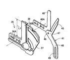
これら図2及び図3において、タグラベル作成装置1は、上記PC118に接続されてPC118からの操作に基づき所望の印字つき無線タグラベルT(後述の図17参照)を作成するものであり、装置本体2(タグラベル作成装置本体)と、この装置本体2の上面に開閉可能に設けられた開閉蓋3と、上記装置本体2の筐体200の側部に設けられた係合部201に対し着脱可能に設けられたアンテナユニット9とを有している。このアンテナユニット9はループアンテナLC(詳細は後述)を内蔵しており、タグラベル作成装置1から取り外された際には、作成装置外の無線タグラベル(無線タグ回路素子To)から無線タグ情報を読み取るための携帯型アンテナとして使用することが可能である(詳細は後述)。   2 and 3, the tag label producing apparatus 1 is connected to the PC 118 and produces a desired RFID label T with print (see FIG. 17 described later) based on an operation from the PC 118. (Tag label producing device main body), the opening / closing lid 3 provided on the upper surface of the device main body 2 so as to be openable and closable, and the engaging portion 201 provided on the side portion of the casing 200 of the device main body 2 so as to be detachable. The antenna unit 9 is provided. The antenna unit 9 incorporates a loop antenna LC (details will be described later). When the antenna unit 9 is detached from the tag label producing apparatus 1, it reads the RFID tag information from the RFID label (RFID circuit element To) outside the producing apparatus. It can be used as a portable antenna for this purpose (details will be described later).

装置本体2は、手前側(図2及び図3中、左手前側)に位置し、装置本体2内で作成された無線タグラベルTを外部に排出するラベル排出口11を備えた側壁10と、この側壁10のうちラベル排出口11の下方に設けられ下端が回動可能に支持された側蓋12とを備えている。   The apparatus main body 2 is located on the front side (the left front side in FIGS. 2 and 3), and includes a side wall 10 having a label discharge port 11 for discharging the RFID label T created in the apparatus main body 2 to the outside. The side cover 10 is provided below the label discharge port 11 in the side wall 10 and has a side lid 12 supported at its lower end so as to be rotatable.

側蓋12は押部13を備えており、この押部13を上方より押し込むことで側蓋12が前方に開放されるようになっている。また、側壁10のうち開閉ボタン4の下方には、タグラベル作成装置1の電源のオン・オフを行う電源ボタン14が設けられている。この電源ボタン14の下方には、装置本体2内に配設された切断機構15(後述の図4等参照)を使用者の手動操作で駆動するためのカッター駆動ボタン16が設けられ、このボタン16が押されることで印字済みタグラベル用テープ109(詳細は後述)を所望の長さにカットして無線タグラベルTを作成するようになっている。   The side lid 12 is provided with a pressing portion 13, and the side lid 12 is opened forward by pushing the pressing portion 13 from above. Further, a power button 14 for turning on / off the power of the tag label producing apparatus 1 is provided below the opening / closing button 4 in the side wall 10. Below the power button 14, a cutter drive button 16 is provided for driving a cutting mechanism 15 (see FIG. 4 described later) disposed in the apparatus main body 2 by a user's manual operation. By pressing 16, the tag label tape 109 with print (details will be described later) is cut to a desired length to produce the RFID label T.

開閉蓋3は、装置本体2の図2及び図3中右奥側の端部にて回動可能に軸支され、バネ等の付勢部材を介して常時開放方向に付勢されている。そして、装置本体2の上面に開閉蓋3に隣接するように配置された開閉ボタン4が押されることにより、開閉蓋3と装置本体2とのロックが解除され、上記付勢部材の作用により開放される。なお、開閉蓋3の中央側部には、透明カバーで覆われた透視窓5が設けられている。   The opening / closing lid 3 is pivotally supported at the end of the apparatus main body 2 at the right rear side in FIGS. 2 and 3 and is always urged in the opening direction via an urging member such as a spring. Then, when the open / close button 4 disposed on the upper surface of the apparatus main body 2 so as to be adjacent to the open / close lid 3 is pressed, the lock between the open / close lid 3 and the apparatus main body 2 is released and opened by the action of the biasing member. Is done. A see-through window 5 covered with a transparent cover is provided at the center side of the opening / closing lid 3.

上記アンテナユニット9は筐体202を有しており、この筐体202内には、無線タグ回路素子To(詳細は後述)との間で無線通信を行うループアンテナLC(ユニット側アンテナ、図2には想像線で概念的に示す)が設けられている。この筐体202は略直方体形状であり、上記装置本体2の係合部201が有する凹部204に対し矢印205方向に差し込まれると、図3に示すように当該凹部204に嵌合される。これにより、アンテナユニット9は装置本体2に装着され、上記ループアンテナLCの通信範囲が、搬送される上記印字済みタグラベル用テープ109に備えられる無線タグ回路素子Toに対し情報送受信可能となるように位置決めされる。なおこのとき、アンテナユニット9が装置本体2に装着されるときと、取り外されたときとで、アンテナユニット9の通信可能範囲が異なるようになっている(詳細は後述)。   The antenna unit 9 has a housing 202, and a loop antenna LC (unit-side antenna, FIG. 2) that performs wireless communication with the RFID circuit element To (described later in detail) is provided in the housing 202. Are shown conceptually in imaginary lines). The casing 202 has a substantially rectangular parallelepiped shape. When the casing 202 is inserted in the direction of the arrow 205 with respect to the concave portion 204 of the engaging portion 201 of the apparatus main body 2, the casing 202 is fitted into the concave portion 204 as shown in FIG. As a result, the antenna unit 9 is attached to the apparatus main body 2 so that the communication range of the loop antenna LC can transmit / receive information to / from the RFID circuit element To provided in the tag label tape 109 to be conveyed. Positioned. At this time, the communicable range of the antenna unit 9 differs between when the antenna unit 9 is attached to the apparatus main body 2 and when it is removed (details will be described later).

凹部204の装置側面側(図2中右下側)には、例えば金属製のシールド板236が設けられている。これにより、凹部204は装置上方に開口した形状となっている。このシールド板236により、図3に示すようにアンテナユニット9を装置本体2に装着した際に、ループアンテナLCより発生する電磁波が装置本体2の外方へ放射するのを抑制できるようになっている。   For example, a metal shield plate 236 is provided on the side surface of the recess 204 (on the lower right side in FIG. 2). Thereby, the recessed part 204 becomes the shape opened to apparatus upper direction. The shield plate 236 can suppress electromagnetic waves generated from the loop antenna LC from radiating outward from the apparatus body 2 when the antenna unit 9 is attached to the apparatus body 2 as shown in FIG. Yes.

また、上記アンテナユニット9の筐体202は、一方側の側面(装置本体2への装着時に装置前方である側壁10側となる面)202bに凸部232を有しており、この凸部232に嵌合する凹部233が装置本体2の係合部201に設けられている。このような構造により、操作者がアンテナユニット9を誤った向きで装置本体2に装着するのを防止するようになっている。また、筐体202の別の側面(図2中右下側の側面)202dには、アンテナユニット9を装置本体2から取り外してタグラベル作成装置1外に存在する無線タグ回路素子Toから情報を読み取る際に、読み取り操作を開始するための操作スイッチ302が設けられている。さらに、筐体202の側面202b及びその反対側側面202cには、操作者が筐体202を把持するための把持部234が適宜の位置に設けられている。これにより、操作者がアンテナユニット9を装置本体2から取り外して携帯型アンテナとして用いる際の把持性や、上記操作スイッチ302を操作するときの操作性・安定性を向上できるようになっている。   The housing 202 of the antenna unit 9 has a convex portion 232 on one side surface (a surface on the side of the side wall 10 that is the front of the device when attached to the apparatus main body 2) 202b. A recess 233 that fits into the device body 2 is provided in the engagement portion 201 of the apparatus main body 2. With such a structure, the operator is prevented from mounting the antenna unit 9 on the apparatus main body 2 in the wrong direction. Further, on another side surface 202d of the casing 202 (the lower right side surface in FIG. 2), the antenna unit 9 is detached from the device main body 2 and information is read from the RFID circuit element To existing outside the tag label producing device 1. At this time, an operation switch 302 for starting a reading operation is provided. Furthermore, a grip portion 234 for an operator to grip the housing 202 is provided at an appropriate position on the side surface 202b and the opposite side surface 202c of the housing 202. As a result, the gripping ability when the operator removes the antenna unit 9 from the apparatus main body 2 and uses it as a portable antenna, and the operability and stability when operating the operation switch 302 can be improved.

また、上記筐体202の側面202bには、略球面形状の凹部206が設けられている。この凹部206には、アンテナユニット9を装置本体2に装着した際に、バネ等の付勢手段207によりこの凹部206に嵌合する方向に付勢された嵌合部材208が嵌合されるようになっている(後述の図4参照)。この嵌合部材208の先端部は上記凹部206に合うように略球面形状となっており、使用者がアンテナユニット9を装置本体2から取り外そうとする場合には、付勢手段207が縮んで嵌合部材208が凹部206から外れ、アンテナユニット9を容易に取り外すことができるようになっている。一方、ループアンテナLCと無線タグ回路素子Toとの通信時には、ソレノイド210(後述の図4等参照)が伸長することにより、嵌合部材208が凹部206に嵌合した状態で固定され、アンテナユニット9と装置本体2の係合部201(凹部204)との係合状態が保持される(言い換えれば、アンテナユニット9が装置本体2へ装着された状態でロックされる)ようになっている。   Further, a substantially spherical recess 206 is provided on the side surface 202b of the housing 202. When the antenna unit 9 is attached to the apparatus main body 2, the fitting member 208 urged in the direction of fitting into the recess 206 by the urging means 207 such as a spring is fitted into the recess 206. (See FIG. 4 described later). The front end portion of the fitting member 208 has a substantially spherical shape so as to fit the concave portion 206, and when the user tries to remove the antenna unit 9 from the apparatus main body 2, the biasing means 207 is contracted. Thus, the fitting member 208 is removed from the recess 206, and the antenna unit 9 can be easily removed. On the other hand, at the time of communication between the loop antenna LC and the RFID circuit element To, the solenoid 210 (see FIG. 4 and the like to be described later) is extended so that the fitting member 208 is fixed in a state where it is fitted in the recess 206, and the antenna unit. 9 and the engaging portion 201 (recessed portion 204) of the apparatus main body 2 are maintained in an engaged state (in other words, the antenna unit 9 is locked while being attached to the apparatus main body 2).

また、アンテナユニット9と装置本体2とを電気的に接続するためのケーブル223(導線部材)が設けられており、このケーブル223を介し装置本体2の送信回路306及び受信回路307とアンテナユニット9のループアンテナLCとのアンテナ共用器240を介した信号の送受信が行われるようになっている(後述の図15参照)。このループアンテナLCは、上記筐体202内における側面202a側寄りに配設されており、磁気誘導(電磁誘導、磁気結合、その他電磁界を介して行われる非接触方式を含む)により上記無線タグ回路素子Toへのアクセス(情報読み取り又は情報書き込み)を行うようになっている。   Further, a cable 223 (conductive member) for electrically connecting the antenna unit 9 and the apparatus main body 2 is provided, and the transmission circuit 306 and the reception circuit 307 of the apparatus main body 2 and the antenna unit 9 are provided via the cable 223. Signals are transmitted / received to / from the loop antenna LC via the antenna duplexer 240 (see FIG. 15 described later). The loop antenna LC is disposed closer to the side surface 202a in the housing 202, and includes the wireless tag by magnetic induction (including electromagnetic induction, magnetic coupling, and other non-contact methods performed via an electromagnetic field). Access (information reading or information writing) to the circuit element To is performed.

図4は、タグラベル作成装置1の内部構造を表す平面図であり、図5は、カートリッジ7の詳細構造を模式的に表す拡大平面図である。   FIG. 4 is a plan view showing the internal structure of the tag label producing apparatus 1, and FIG. 5 is an enlarged plan view schematically showing the detailed structure of the cartridge 7.

これら図4及び図5において、内部ユニット20は、概略的には、カートリッジ7を収納するカートリッジホルダ6と、印字手段としての印字ヘッド(サーマルヘッド)23を備えた印字機構21と、切断機構15と、ハーフカットユニット35(後述の図9等参照)と、生成された無線タグラベルT(後述の図18参照)をラベル排出口11(図2及び図3参照)より排出するラベル排出機構22とを備えている。   4 and 5, the internal unit 20 schematically includes a cartridge holder 6 that accommodates the cartridge 7, a printing mechanism 21 that includes a printing head (thermal head) 23 as a printing unit, and a cutting mechanism 15. And a label discharge mechanism 22 for discharging the generated RFID label T (see FIG. 18 described later) from the label discharge port 11 (see FIGS. 2 and 3), and a half cut unit 35 (see FIG. 9 described later). It has.

上記カートリッジホルダ6は、ラベル排出口11から排出される印字済みタグラベル用テープ109の印字面が、垂直方向となるようにカートリッジ7を収納する。   The cartridge holder 6 accommodates the cartridge 7 so that the printing surface of the tag label tape 109 with print discharged from the label discharge port 11 is in the vertical direction.

カートリッジ7は、筐体7Aと、この筐体7A内に配置され帯状の基材テープ101が巻回された第1ロール102と、上記基材テープ101と略同じ幅である透明な上記カバーフィルム103が巻回された第2ロール104と、インクリボン105(熱転写リボン、但し被印字テープが感熱テープの場合は不要)を繰り出すリボン供給側ロール111と、印字後のリボン105を巻取るリボン巻取りローラ106と、カートリッジ7のテープ排出部30の近傍に回転可能に支持されたテープ送りローラ27と、搬送位置規制手段として機能するガイドローラ112とを有する。   The cartridge 7 includes a housing 7 </ b> A, a first roll 102 that is disposed in the housing 7 </ b> A and has a belt-like base tape 101 wound thereon, and the transparent cover film that has substantially the same width as the base tape 101. Ribbon supply side roll 111 that feeds out second ribbon 104 around which 103 is wound, ink ribbon 105 (thermal transfer ribbon, but not required when the print-receiving tape is a thermal tape), and ribbon winding that winds up ribbon 105 after printing A take-up roller 106, a tape feed roller 27 rotatably supported in the vicinity of the tape discharge portion 30 of the cartridge 7, and a guide roller 112 functioning as a transport position regulating means.

テープ送りローラ27は、上記基材テープ101と上記カバーフィルム103とを押圧し接着させ上記印字済タグラベル用テープ109としつつ、矢印Aで示す方向にテープ送りを行う(=圧着ローラとしても機能する)。   The tape feed roller 27 presses and bonds the base tape 101 and the cover film 103 to form the printed tag label tape 109 and feeds the tape in the direction indicated by the arrow A (= also functions as a pressure roller). ).

第1ロール102は、リール部材102aの周りに、長手方向に複数の無線タグ回路素子Toが所定の等間隔で順次形成された上記基材テープ101を巻回している。基材テープ101はこの例では4層構造となっており(図5中部分拡大図参照)、内側に巻かれる側(図5中右側)よりその反対側(図5中左側)へ向かって、適宜の粘着材からなる粘着層101a、PET(ポリエチレンテレフタラート)等から成る色付きのベースフィルム101b、適宜の粘着材からなる粘着層101c、剥離紙101dの順序で積層され構成されている。   The first roll 102 is wound with the base tape 101 in which a plurality of RFID tag circuit elements To are sequentially formed at predetermined equal intervals in the longitudinal direction around a reel member 102a. In this example, the base tape 101 has a four-layer structure (see a partially enlarged view in FIG. 5), from the side wound inside (right side in FIG. 5) to the opposite side (left side in FIG. 5), An adhesive layer 101a made of an appropriate adhesive material, a colored base film 101b made of PET (polyethylene terephthalate), an adhesive layer 101c made of an appropriate adhesive material, and a release paper 101d are laminated in this order.

ベースフィルム101bの裏側(図5中左側)には、ループコイル形状に構成され情報の送受信を行うループアンテナ152(タグ側アンテナ)がこの例では一体的に設けられており、これに接続するように情報を記憶するIC回路部151が形成され、これらによって無線タグ回路素子Toが構成されている。   On the back side (left side in FIG. 5) of the base film 101b, a loop antenna 152 (tag side antenna) configured in a loop coil shape and transmitting / receiving information is integrally provided in this example, and is connected thereto. The IC circuit portion 151 for storing information is formed, and the RFID tag circuit element To is constituted by these.

ベースフィルム101bの表側(図5中右側)には、後にカバーフィルム103を接着するための上記粘着層101aが形成され、またベースフィルム101bの裏側(図5中左側)には、無線タグ回路素子Toを内包するように設けた上記粘着層101cによって上記剥離紙101dがベースフィルム101bに接着されている。   The adhesive layer 101a for later bonding the cover film 103 is formed on the front side (right side in FIG. 5) of the base film 101b, and the RFID circuit element is formed on the back side (left side in FIG. 5) of the base film 101b. The release paper 101d is bonded to the base film 101b by the adhesive layer 101c provided so as to enclose To.

剥離紙101dは、最終的にラベル状に完成した無線タグラベルTが所定の商品等に貼り付けられる際に、これを剥がすことで粘着層101cにより当該商品等に接着できるようにしたものである。また、この剥離紙101dの表面には、各無線タグ回路素子Toに対応した所定の位置に、搬送制御用の所定の識別子(この例では黒塗りの識別子。あるいはレーザ加工等により基材テープ101を貫通する孔を穿孔する等でもよい。又はトムソン型での加工穴等でもよい)PM(検出対象部位)が設けられている。   The release paper 101d is configured such that when the RFID label T finally completed in a label shape is attached to a predetermined product or the like, the release paper 101d can be adhered to the product or the like by the adhesive layer 101c by peeling it off. Further, on the surface of the release paper 101d, a predetermined identifier for transport control (in this example, a black identifier, or a base tape 101 by laser processing or the like) is provided at a predetermined position corresponding to each RFID circuit element To. A hole penetrating through the hole may be drilled, or a Thomson-type hole or the like) may be provided.

第2ロール104は、リール部材104aの周りに上記カバーフィルム103を巻回している。第2ロール104より繰り出されるカバーフィルム103は、その裏面側(すなわち上記基材テープ101と接着される側)に配置された上記リボン供給側ロール111及び上記リボン巻取りローラ106で駆動されるリボン105が、上記印字ヘッド23に押圧されることで当該カバーフィルム103の裏面に当接させられるようになっている。   The second roll 104 has the cover film 103 wound around a reel member 104a. The cover film 103 fed out from the second roll 104 is a ribbon driven by the ribbon supply side roll 111 and the ribbon take-up roller 106 arranged on the back side thereof (that is, the side to be bonded to the base tape 101). 105 is pressed against the print head 23 to be brought into contact with the back surface of the cover film 103.

リボン巻取りローラ106及びテープ送りローラ27は、それぞれカートリッジ7外に設けた例えばパルスモータである搬送用モータ119(後述の図15参照)の駆動力が図示しないギヤ機構を介しリボン巻取りローラ駆動軸107及びテープ送りローラ駆動軸108に伝達されることによって連動して回転駆動される。   The ribbon take-up roller 106 and the tape feed roller 27 are driven by a ribbon take-up roller via a gear mechanism (not shown) driven by a conveying motor 119 (see FIG. 15 to be described later), for example, a pulse motor provided outside the cartridge 7. By being transmitted to the shaft 107 and the tape feed roller drive shaft 108, they are driven to rotate in conjunction with each other.

一方このとき、多数の発熱素子を備えた上記印字ヘッド23が、カートリッジホルダ6に立設されたヘッド取付部24に取り付けられて、テープ送りローラ27よりカバーフィルム103の搬送方向上流側に配置されている。   On the other hand, at this time, the print head 23 having a large number of heat generating elements is attached to the head attaching portion 24 erected on the cartridge holder 6 and arranged upstream of the tape feed roller 27 in the transport direction of the cover film 103. ing.

また、カートリッジホルダ6のうちカートリッジ7の前方(図4中、下側)には、ローラホルダ25が支持軸29により回動可能に枢支され、切換機構により印字位置(当接位置、図4参照)とリリース位置(離反位置)とに切換可能とされている。このローラホルダ25には、プラテンローラ26及びテープ圧接ローラ28が回転可能に配設されており、ローラホルダ25が上記印字位置に切り換えられたときに、それらプラテンローラ26及びテープ圧接ローラ28が上記印字ヘッド23及び上記テープ送りローラ27に対し圧接されるようになっている。   Further, a roller holder 25 is pivotally supported by a support shaft 29 in front of the cartridge 7 in the cartridge holder 6 (lower side in FIG. 4), and a printing position (contact position, FIG. Reference) and a release position (separation position). In the roller holder 25, a platen roller 26 and a tape pressure roller 28 are rotatably arranged. When the roller holder 25 is switched to the printing position, the platen roller 26 and the tape pressure roller 28 are The print head 23 and the tape feed roller 27 are pressed against each other.

上記構成において、上記第1ロール102より繰り出された基材テープ101は、テープ送りローラ27へと供給される。一方、第2ロール104より繰り出されるカバーフィルム103は、その裏面側(すなわち上記基材テープ101と接着される側)に配置されリボン供給側ロール111とリボン巻取りローラ106とにより駆動されるインクリボン105が、上記印字ヘッド23に押圧されて当該カバーフィルム103の裏面に当接させられる。   In the above configuration, the base tape 101 fed out from the first roll 102 is supplied to the tape feed roller 27. On the other hand, the cover film 103 fed out from the second roll 104 is arranged on the back side thereof (that is, the side to be bonded to the base tape 101), and is driven by the ribbon supply side roll 111 and the ribbon take-up roller 106. The ribbon 105 is pressed against the print head 23 and brought into contact with the back surface of the cover film 103.

そして、カートリッジ7が上記カートリッジホルダ6に装着されロールホルダ25が上記リリース位置から上記印字位置に移動されると、カバーフィルム103及びインクリボン105が印字ヘッド23とプラテンローラ26との間に狭持されるとともに、基材テープ101及びカバーフィルム103がテープ送りローラ27と圧着ローラ28との間に狭持される。そして、搬送用モータ119の駆動力によってリボン巻取りローラ106及びテープ送りローラ27が矢印B及び矢印Cで示す方向にそれぞれ同期して回転駆動される。このとき、前述のテープ送りローラ駆動軸108と上記圧着ローラ28及びプラテンローラ26はギヤ機構(図示せず)にて連結されており、テープ送りローラ駆動軸108の駆動に伴いテープ送りローラ27、圧着ローラ28、及びプラテンローラ26が回転し、第1ロール102から基材テープ101が繰り出され、上述のようにテープ送りローラ27へ供給される。一方、第2ロール104からはカバーフィルム103が繰り出されるとともに、印刷駆動回路120(後述の図15参照)により印字ヘッド23の複数の発熱素子が通電される。この結果、カバーフィルム103の裏面に、貼り合わせ対象となる基材テープ101上の無線タグ回路素子Toの記憶情報に対応したラベル印字R(後述の図17参照)が印刷される。そして、上記基材テープ101と上記印刷が終了したカバーフィルム103とが上記テープ送りローラ27及び圧着ローラ28により接着されて一体化されて印字済タグラベル用テープ109として形成され、テープ排出部30よりカートリッジ7外へと搬出される。カバーフィルム103への印字が終了したインクリボン105は、リボン巻取りローラ駆動軸107の駆動によりリボン巻取りローラ106に巻取られる。   When the cartridge 7 is mounted on the cartridge holder 6 and the roll holder 25 is moved from the release position to the print position, the cover film 103 and the ink ribbon 105 are held between the print head 23 and the platen roller 26. At the same time, the base tape 101 and the cover film 103 are sandwiched between the tape feeding roller 27 and the pressure roller 28. Then, the ribbon take-up roller 106 and the tape feed roller 27 are rotationally driven in synchronization with the directions indicated by the arrows B and C by the driving force of the conveying motor 119, respectively. At this time, the tape feed roller drive shaft 108, the pressure roller 28 and the platen roller 26 are connected by a gear mechanism (not shown), and the tape feed roller 27, The pressure roller 28 and the platen roller 26 rotate, and the base tape 101 is fed out from the first roll 102 and supplied to the tape feed roller 27 as described above. On the other hand, the cover film 103 is fed out from the second roll 104, and a plurality of heating elements of the print head 23 are energized by the print drive circuit 120 (see FIG. 15 described later). As a result, a label print R (see FIG. 17 described later) corresponding to the stored information of the RFID circuit element To on the base tape 101 to be bonded is printed on the back surface of the cover film 103. The base tape 101 and the cover film 103 after printing are bonded and integrated by the tape feeding roller 27 and the pressure roller 28 to form a tag label tape 109 with print. It is carried out of the cartridge 7. The ink ribbon 105 that has finished printing on the cover film 103 is taken up by the ribbon take-up roller 106 by driving the ribbon take-up roller drive shaft 107.

なお、カートリッジ7の上記筐体7Aの上面には、例えば、カートリッジ7内に内蔵されている上記基材テープ101のテープ幅、テープの色等を表示するテープ特定表示部8が設けられている。カートリッジ7をカートリッジホルダ6に装着して開閉蓋3を閉じると、前述の透視窓5とテープ特定表示部8とが相互に対向し、透視窓5の透明カバーを介してテープ特定表示部8を装置本体2の外部から視認できる。これにより、カートリッジホルダ6に装着されているカートリッジ7の種類等を装置本体2の外部から透視窓5を介して容易に視認できるようになっている。   Note that, on the upper surface of the housing 7A of the cartridge 7, for example, a tape specifying display portion 8 for displaying the tape width of the base tape 101 incorporated in the cartridge 7 and the color of the tape is provided. . When the cartridge 7 is attached to the cartridge holder 6 and the opening / closing lid 3 is closed, the above-described see-through window 5 and the tape specifying display unit 8 face each other, and the tape specifying display unit 8 is opened via the transparent cover of the see-through window 5. Visible from the outside of the apparatus body 2. As a result, the type of the cartridge 7 attached to the cartridge holder 6 can be easily visually recognized from the outside of the apparatus main body 2 through the transparent window 5.

一方、前述したように、内部ユニット20には、上記切断機構15と、上記ラベル排出機構22とが備えられ、さらに、これら切断機構15とラベル排出機構22との間にアンテナユニット9が装着される。また、切断機構15とラベル排出機構22の間には、装着されたアンテナユニット9と印字済タグラベル用テープ109の搬送経路を挟んで反対側となる位置に、例えばフェライト等からなる磁性部材235が設けられている。これにより、ループアンテナLCで発生される磁路を集中させ、ループアンテナLCの通信対象となる無線タグ回路素子Toへの効率の良い通信を可能としつつ、それ以外の無線タグ回路素子To(すなわち、例えばカートリッジ7内の無線タグ回路素子To等)への通信を抑制するようになっている。なお、ここでは磁性部材をループアンテナLCと印字済タグラベル用テープ109の搬送経路を挟んで反対側となる位置に設けるようにしたが、これに限られず、例えば搬送経路の両側に配設するようにしてもよい。   On the other hand, as described above, the internal unit 20 includes the cutting mechanism 15 and the label discharge mechanism 22, and the antenna unit 9 is mounted between the cutting mechanism 15 and the label discharge mechanism 22. The Further, between the cutting mechanism 15 and the label discharge mechanism 22, a magnetic member 235 made of, for example, ferrite is provided at a position on the opposite side across the transport path of the mounted antenna unit 9 and the printed tag label tape 109. Is provided. As a result, the magnetic path generated by the loop antenna LC is concentrated, enabling efficient communication to the RFID circuit element To that is the communication target of the loop antenna LC, while other RFID circuit elements To (that is, For example, communication to the RFID circuit element To in the cartridge 7) is suppressed. In this case, the magnetic member is provided at a position on the opposite side across the conveyance path of the loop antenna LC and the printed tag label tape 109. However, the present invention is not limited to this. For example, the magnetic member may be disposed on both sides of the conveyance path. It may be.

そして、印字済みタグラベル用テープ109に対しループアンテナLCにより無線タグ回路素子Toに情報読み取り又は書き込みが行われた後、自動的にあるいは上記カッター駆動ボタン16(図2及び図3参照)を操作することにより切断機構15によって印字済みタグラベル用テープ109が切断されて無線タグラベルTが生成される。この無線タグラベルTは、その後さらにラベル排出機構22によって側壁10(図2及び図3参照)に形成されたラベル排出口11から排出されるようになっている。   Then, after the information is read or written to the RFID circuit element To by the loop antenna LC with respect to the tag label tape 109 with print, the cutter driving button 16 (see FIGS. 2 and 3) is operated automatically. As a result, the tag label tape 109 with print is cut by the cutting mechanism 15 and the RFID label T is generated. The RFID label T is then discharged from the label discharge port 11 formed in the side wall 10 (see FIGS. 2 and 3) by the label discharge mechanism 22.

上記切断機構15は、固定刃40と、この固定刃40とともにカット動作を行う可動刃41と、この可動刃41に連結されるカッターハスバギヤ42(後述の図8等参照)と、このカッターハスバギヤ42にギヤ列により連結されるカッターモータ43(後述の図15参照)とを備えている。   The cutting mechanism 15 includes a fixed blade 40, a movable blade 41 that performs a cutting operation together with the fixed blade 40, a cutter helical gear 42 (see FIG. 8 and the like described later) connected to the movable blade 41, A cutter motor 43 (see FIG. 15 described later) connected to the gear 42 by a gear train is provided.

上記ラベル排出機構22は、装置本体2の側壁10に設けられたラベル排出口11の近傍に配設され、切断機構15において切断された後の印字済みタグラベル用テープ109(言い換えれば無線タグラベルT、以下同様)をラベル排出口11から強制的に排出するための排出手段としての機能を有する。すなわち、ラベル排出機構22は、駆動ローラ51(搬送手段)と、この駆動ローラ51に対して印字済みタグラベル用テープ109を挟んで対向する押圧ローラ52と、この押圧ローラ52を印字済みタグラベル用テープ109に対して押圧し、またはその押圧を解除するように作動される押圧作動機構部53(図示せず)と、この押圧作動機構部53の押圧解除動作に連動して、駆動ローラ51により印字済みタグラベル用テープ109を排出するように回転させるための排出駆動機構部54(図示せず)とを備えている。また、ラベル排出機構22は、印字済みタグラベル用テープ109の上記剥離紙101dに設けられた識別マークPMを検出するマークセンサ127(後述の図7等参照)を有している。   The label discharge mechanism 22 is disposed in the vicinity of the label discharge port 11 provided in the side wall 10 of the apparatus main body 2 and is printed with the tag label tape 109 (in other words, the RFID label T, The same applies hereinafter) functioning as discharge means for forcibly discharging from the label discharge port 11. That is, the label discharge mechanism 22 includes a driving roller 51 (conveying means), a pressing roller 52 facing the driving roller 51 with a printed tag label tape 109 interposed therebetween, and the pressing roller 52 as a printed tag label tape. A pressure actuating mechanism 53 (not shown) that is actuated so as to depress or release the pressure, and printing is performed by the drive roller 51 in conjunction with the depressing operation of the press actuating mechanism 53. A discharge driving mechanism 54 (not shown) for rotating the tag label tape 109 so as to be discharged is provided. Further, the label discharge mechanism 22 has a mark sensor 127 (see FIG. 7 described later) for detecting the identification mark PM provided on the release paper 101d of the tag label tape 109 with print.

このとき、上記ラベル排出口11の内側には、印字済みタグラベル用テープ109をラベル排出口11へ案内するための第1案内壁55,56及び第2案内壁63,64が設けられている(図4参照)。第1案内壁55,56及び第2案内壁63,64はそれぞれ一体に形成され、上記固定刃40と可動刃41とでカットされた印字済みタグラベル用テープ109の排出位置において、互いに所定の間隔を隔てられるように配置されている。   At this time, first guide walls 55 and 56 and second guide walls 63 and 64 for guiding the tag label tape 109 with print to the label discharge port 11 are provided inside the label discharge port 11 ( (See FIG. 4). The first guide walls 55 and 56 and the second guide walls 63 and 64 are integrally formed, and at a discharge position of the tag label tape 109 with print cut by the fixed blade 40 and the movable blade 41, a predetermined distance from each other. It is arranged to be separated.

図6は、上記第1ロール102より繰り出された基材テープ101に備えられる無線タグ回路素子Toの概念的構成を表す、図5中矢印D方向から見た概念図である。この図6において、無線タグ回路素子Toは、ループコイル形状に構成され情報の送受信を行う上記ループアンテナ152と、これに接続され情報を記憶するIC回路部151とから構成されている。   FIG. 6 is a conceptual diagram showing the conceptual configuration of the RFID circuit element To provided in the base tape 101 fed out from the first roll 102, as viewed from the direction of arrow D in FIG. In FIG. 6, the RFID circuit element To is composed of the loop antenna 152 that is configured in a loop coil shape and transmits / receives information, and an IC circuit unit 151 that is connected thereto and stores information.

図7(a)は、ラベル排出機構22の要部詳細構造を表す部分抽出斜視図であり、図7(b)はマークセンサ127の概念的構成を表す図である。図7(a)において、上記第1案内壁55,56の上下方向途中部が切り欠かれ、一方の第1案内壁55には、上記駆動ローラ51が、切欠部から印字済みタグラベル用テープ109の排出位置に臨むようにして設けられている。なお、駆動ローラ51は、その上面に同心円状の溝により形成されたローラ切り欠き部51Aを有する。一方、他方の第1案内壁56には、押圧ローラ52が、切欠部から印字済みタグラベル用テープ109の排出位置に臨むようにして、上記押圧作動機構部53のローラ支持部58に支持されている。   FIG. 7A is a partial extraction perspective view showing a detailed structure of a main part of the label discharge mechanism 22, and FIG. 7B is a view showing a conceptual configuration of the mark sensor 127. In FIG. 7A, the middle portions of the first guide walls 55 and 56 in the vertical direction are notched, and the drive roller 51 is provided on one of the first guide walls 55 from the notched portion to the tag label tape 109 with print. It is provided so as to face the discharge position. The drive roller 51 has a roller cutout 51A formed by a concentric groove on the upper surface thereof. On the other hand, on the other first guide wall 56, the pressing roller 52 is supported by the roller support portion 58 of the pressing operation mechanism portion 53 so as to face the discharging position of the tag label tape 109 with print from the notch portion.

また、駆動ローラ51よりも搬送方向上流側には、上記基材テープ101の剥離紙101dに各無線タグ回路素子Toの位置に対応して設けた適宜の識別マークPM(図6等参照)を検出可能なマークセンサ127が設けられている。このマークセンサ127は、図7(b)に示すように、例えば発光ダイオードからなる投光器127a及びフォトトランジスタからなる受光器127bから構成される反射型の公知の光電センサである。投光器127aと受光器127bとの間に上記識別マークPMが存在するかどうかに応じて、受光器127bからの制御出力が反転させられるようになっている。なお、マークセンサ127としては、上記反射型に限らず、透過型の光電センサを用いてもよい。   Further, an appropriate identification mark PM (see FIG. 6 or the like) provided on the release paper 101d of the base tape 101 corresponding to the position of each RFID circuit element To is upstream of the driving roller 51 in the transport direction. A detectable mark sensor 127 is provided. As shown in FIG. 7B, the mark sensor 127 is a known reflection type photoelectric sensor including a projector 127a made of a light emitting diode and a light receiver 127b made of a phototransistor, for example. The control output from the light receiver 127b is inverted depending on whether or not the identification mark PM exists between the light projector 127a and the light receiver 127b. The mark sensor 127 is not limited to the reflective type, and a transmissive photoelectric sensor may be used.

図8は、図4に示した構造からラベル排出機構22及びアンテナユニット9を取り外した状態における内部ユニット20の外観を表す斜視図である。   FIG. 8 is a perspective view showing an appearance of the internal unit 20 in a state where the label discharge mechanism 22 and the antenna unit 9 are removed from the structure shown in FIG.

図8において、上記カッターハスバギヤ42には、突起状に形成されたボス50が設けられ、このボス50が上記可動刃41の長孔49に挿入されるように構成されている(後述の図9や図10も参照)。また、テープ排出方向に沿って固定刃40及び可動刃41の下流側には、ハーフカットユニット35が取り付けられている。   In FIG. 8, the cutter helical gear 42 is provided with a boss 50 formed in a projecting shape, and this boss 50 is configured to be inserted into a long hole 49 of the movable blade 41 (described later). 9 and FIG. 10). A half cut unit 35 is attached to the downstream side of the fixed blade 40 and the movable blade 41 along the tape discharging direction.

ハーフカットユニット35は、固定刃40に合わせて配置される受け台38と、この受け台38と対向し可動刃41側に配置されるハーフカッタ34と、固定刃40と受け台38との間に固定刃40と合わせて配置される第1ガイド部36と、この第1ガイド部36と対向し可動刃41と合わせて配置される第2ガイド部37とから構成される(後述の図11も参照)。第1ガイド部36及び第2ガイド部37は一体に構成され、固定刃40の固定孔40Aに対応する位置に設けられたガイド固定部36Aにより固定刃40とともに側板44(図4参照)に取り付けられている。   The half-cut unit 35 includes a cradle 38 that is arranged in accordance with the fixed blade 40, a half cutter 34 that is opposed to the cradle 38 and is disposed on the movable blade 41 side, and between the fixed blade 40 and the cradle 38. The first guide portion 36 is disposed in combination with the fixed blade 40, and the second guide portion 37 is disposed in combination with the movable blade 41 so as to face the first guide portion 36 (see FIG. 11 described later). See also). The first guide portion 36 and the second guide portion 37 are integrally formed, and are attached to the side plate 44 (see FIG. 4) together with the fixed blade 40 by a guide fixing portion 36A provided at a position corresponding to the fixed hole 40A of the fixed blade 40. It has been.

このとき、ハーフカッタ34を所定の回動支点(図示せず)を中心として回動させるために、ハーフカッタモータ129(図示省略。後述の図15参照)が設けられている。このハーフカッタモータ129を用いたハーフカッタ34の駆動機構は、詳細な図示を省略するが、例えば以下のように構成することができる。すなわち、例えばハーフカッタモータ129を正逆回転可能な電動モータで構成し、ギヤ列(図示せず)を介してピン(同)を備えたクランク部材(同)に接続し、ランク部材の上記ピンが係合するための長溝をハーフカッタ34に穿設しておく。そして、ハーフカッタモータ129の駆動力によりクランク部材を回動させたとき、クランク部材の上記ピンが長溝に沿って移動することにより、ハーフカッタ34を所定の方向(時計回り又は反時計回り)方向に回動させることができる。   At this time, a half cutter motor 129 (not shown; see FIG. 15 described later) is provided to rotate the half cutter 34 around a predetermined rotation fulcrum (not shown). The driving mechanism of the half cutter 34 using the half cutter motor 129 is not shown in detail, but can be configured as follows, for example. That is, for example, the half cutter motor 129 is constituted by an electric motor capable of rotating forward and reverse, and is connected to a crank member (same) provided with a pin (same) via a gear train (not shown), and the above-mentioned pin of the rank member A long groove for engaging is formed in the half cutter 34. When the crank member is rotated by the driving force of the half cutter motor 129, the pin of the crank member moves along the long groove, thereby causing the half cutter 34 to move in a predetermined direction (clockwise or counterclockwise). Can be rotated.

受け台38は、テープ排出部30より排出される印字済みタグラベル用テープ109に対向する端部がテープに平行になるように折曲され、受け面38Bを形成している。ここで、印字済みタグラベル用テープ109は、前述のように、カバーフィルム103と、粘着層101a、ベースフィルム101b、粘着層101c、剥離紙101dからなる4層構造の基材テープ101が貼り合わされることで5層構造となっている(後述の図18も参照)。そして、上記のようにしてハーフカッタモータ129の駆動力を用いて上記ハーフカッタ34を受け面38Bに押し付けることにより、ハーフカッタ34と受け面38Bとの間にある印字済みタグラベル用テープ109は、カバーフィルム103、粘着層101a、ベースフィルム101b、粘着層101cは切断されるが、剥離紙101dのみが切り残されてテープ幅方向に略沿ってハーフカット線HC(後述の図17等参照)が形成される。なお、ハーフカッタ34が受け面38Bに接当した後は、例えば前述の構成においてはギヤ列に介装された図示しない滑りクラッチにより、ハーフカッタモータ129に過負荷が生じないように構成することが好ましい。この受け面38Bは、第1案内部55、56とともに印字済みタグラベル用テープ109をラベル排出口11へ案内する役割も有する。   The cradle 38 is bent so that an end facing the tag label tape 109 with print discharged from the tape discharge unit 30 is parallel to the tape, and forms a receiving surface 38B. Here, as described above, the tag label tape 109 with print is bonded to the cover film 103 and the base tape 101 having a four-layer structure including the adhesive layer 101a, the base film 101b, the adhesive layer 101c, and the release paper 101d. Thus, a five-layer structure is formed (see also FIG. 18 described later). Then, by pressing the half cutter 34 against the receiving surface 38B using the driving force of the half cutter motor 129 as described above, the tag label tape 109 with print between the half cutter 34 and the receiving surface 38B is The cover film 103, the adhesive layer 101a, the base film 101b, and the adhesive layer 101c are cut, but only the release paper 101d is left uncut and a half-cut line HC (see FIG. 17 and the like described later) substantially along the tape width direction. It is formed. In addition, after the half cutter 34 contacts the receiving surface 38B, for example, in the above-described configuration, the half cutter motor 129 is configured not to be overloaded by a not-shown slip clutch interposed in the gear train. Is preferred. The receiving surface 38 </ b> B has a role of guiding the tag label tape 109 with print to the label discharge port 11 together with the first guide portions 55 and 56.

図9及び図10は、内部ユニット20より上記ハーフカッタ34を除去した、切断機構15の外観を表す斜視図である。   9 and 10 are perspective views showing the appearance of the cutting mechanism 15 in which the half cutter 34 is removed from the internal unit 20.

これら図9及び図10において、切断機構15では、カッターモータ43(図15参照)によりカッターハスバギヤ42が回転した際に、可動刃41がボス50と長孔49により軸孔48を支点として揺動し、印字済みタグラベル用テープ109がカットされるようになっている。   9 and 10, in the cutting mechanism 15, when the cutter helical gear 42 is rotated by the cutter motor 43 (see FIG. 15), the movable blade 41 is swung around the shaft hole 48 by the boss 50 and the long hole 49. The tag label tape 109 with print is cut.

すなわちまず、カッターハスバギヤ42のボス50が内側(図9中、左側)に位置する場合においては可動刃41は固定刃40から離れて位置する(以下この状態を初期状態とする。図9参照)。そして、この初期状態においてカッターモータ43が駆動し、カッターハスバギヤ42が反時計回り(矢印70方向)に回転すると、ボス50が外側に移動するとともに、可動刃41は軸孔48を中心に反時計回り(矢印73方向)に回動し、内部ユニット20に固定された固定刃40とで印字済みタグラベル用テープ109を切断する(以下この状態を切断状態とする。図10参照)。   That is, first, when the boss 50 of the cutter helical gear 42 is positioned on the inner side (left side in FIG. 9), the movable blade 41 is positioned away from the fixed blade 40 (hereinafter, this state is referred to as an initial state). ). In this initial state, when the cutter motor 43 is driven and the cutter helical gear 42 rotates counterclockwise (in the direction of the arrow 70), the boss 50 moves outward and the movable blade 41 counters around the shaft hole 48. The tag label tape 109 with print is cut with the fixed blade 40 fixed to the internal unit 20 by rotating clockwise (in the direction of arrow 73) (this state is hereinafter referred to as a cut state, see FIG. 10).

このようにして印字済みタグラベル用テープ109を切断して無線タグラベルを生成した後には、次回搬送される印字済みタグラベル用テープ109を切断するために可動刃41を初期状態に戻す必要がある。従って、再びカッターモータ43を駆動し、カッターハスバギヤ42を反時計回り(矢印70方向)に回転させることで、再びボス50が内側に移動するとともに、可動刃41は時計回り(矢印74方向)に回動し、可動刃41を固定刃40から離間させる(図9参照)。そして、次回、カートリッジ7より印字され搬送される印字済みタグラベル用テープ109を切断可能な状態となる。   After the printed tag label tape 109 is cut in this way to generate the RFID label, it is necessary to return the movable blade 41 to the initial state in order to cut the printed tag label tape 109 to be conveyed next time. Therefore, by driving the cutter motor 43 again and rotating the cutter helical gear 42 counterclockwise (in the direction of arrow 70), the boss 50 moves inward again, and the movable blade 41 rotates in the clockwise direction (in the direction of arrow 74). To move the movable blade 41 away from the fixed blade 40 (see FIG. 9). Then, the tag label tape 109 with print, which is printed and conveyed from the cartridge 7 next time, can be cut.

なおこのとき、カッターハスバギヤ42の円筒外壁上にはカッターハスバギヤ用カム42Aが設けられ、カッターモータ43によりカッターハスバギヤ42が回転すると、カッターハスバギヤ用カム42Aの作用によりカッターハスバギヤ42に隣接して設けられたマイクロスイッチ126がオフ状態からオン状態に切り替わる。それにより、印字済みタグラベル用テープ109の切断状態が検出されるようになっている。   At this time, the cutter helical gear cam 42A is provided on the cylindrical outer wall of the cutter helical gear 42, and when the cutter helical gear 42 is rotated by the cutter motor 43, the cutter helical gear 42 is moved to the cutter helical gear 42 by the action of the cutter helical gear cam 42A. The adjacent microswitch 126 is switched from the off state to the on state. Thereby, the cut state of the tag label tape 109 with print is detected.

図11は、上記可動刃41及び固定刃40の詳細構造を上記ハーフカットユニット35ともに表す斜視図であり、図12はその部分拡大断面図である。これら図11及び図12において、固定刃40は、印字機構15内のカートリッジホルダ6の左側において起立状に設けられる側板44(図4参照)に固定孔40Aを通してネジ等により固定されている。   FIG. 11 is a perspective view showing the detailed structure of the movable blade 41 and the fixed blade 40 together with the half-cut unit 35, and FIG. 12 is a partially enlarged sectional view thereof. 11 and 12, the fixed blade 40 is fixed to a side plate 44 (see FIG. 4) provided upright on the left side of the cartridge holder 6 in the printing mechanism 15 with a screw or the like through a fixing hole 40A.

可動刃41は、略V字状をなし、切断部分に設けられた刃部45と刃部45の反対に位置する柄部46と屈曲部47とから構成される。屈曲部47には上記軸孔48が設けられ、この屈曲部47を支点として可動刃41が回動できるように軸孔48にて側板44に支持されている。また、可動刃41の切断部分に設けられた刃部45の反対側の柄部46に上記長孔49が形成されている。刃部45は2段刃により形成されており、その刃面は刃部45の厚みを徐々に薄くする第1傾斜面45Aと第2傾斜面45Bの傾斜角度の異なる2つの傾斜面により構成されている。   The movable blade 41 is substantially V-shaped and includes a blade portion 45 provided at a cutting portion, a handle portion 46 positioned opposite to the blade portion 45, and a bent portion 47. The bent portion 47 is provided with the shaft hole 48, and is supported by the side plate 44 at the shaft hole 48 so that the movable blade 41 can rotate with the bent portion 47 as a fulcrum. Further, the elongated hole 49 is formed in the handle 46 on the opposite side of the blade 45 provided at the cutting portion of the movable blade 41. The blade portion 45 is formed by a two-stage blade, and the blade surface is constituted by two inclined surfaces having different inclination angles of the first inclined surface 45A and the second inclined surface 45B that gradually reduce the thickness of the blade portion 45. ing.

一方、前述のハーフカットユニット35の上記第1ガイド部36のうち、排出される印字済みタグラベル用テープ109に対向する端部36Bは、上記受け台38の端部に形成された受け面38Bに沿って突出され、且つ印字済みタグラベル用テープ109の排出方向へ折曲されている。従って、第1ガイド部36の端部36Bは、カートリッジ7より排出される印字済みタグラベル用テープ109に対する接面36Cにおいて印字済みタグラベル用テープ109排出方向に対して滑らかな曲面を有する。   On the other hand, of the first guide portion 36 of the half-cut unit 35 described above, the end portion 36B facing the printed tag label tape 109 is a receiving surface 38B formed at the end portion of the receiving base 38. And the tag label tape 109 with print is bent in the discharging direction. Therefore, the end portion 36B of the first guide portion 36 has a smooth curved surface with respect to the printed tag label tape 109 discharging direction at the contact surface 36C with respect to the printed tag label tape 109 discharged from the cartridge 7.

第1ガイド部36の端部36Bを突出させ接面36Cを曲面としたことにより、一定曲率以上にカールした印字済みタグラベル用テープ109の先端部は、先ず第1ガイド部36の接面36Cに当たる。その際に、印字済みタグラベル用テープ109の先端部が第1ガイド部の接面36C上の境界点75より印字済みタグラベル用テープ109の排出方向の下流側(図12中、下方向)に当たった場合には、印字済みタグラベル用テープ109の先端部はその曲面に沿って下流側へ移動することで、固定刃40と第1ガイド部36や受け台38の間に侵入することなく、ラベル排出口11方向へ導くようになっている。   By projecting the end portion 36B of the first guide portion 36 and making the contact surface 36C curved, the front end portion of the tag label tape 109 with print curled to a certain curvature or more first hits the contact surface 36C of the first guide portion 36. . At this time, the leading end of the tag label tape 109 with print hits the downstream side (downward in FIG. 12) of the printed tag label tape 109 from the boundary point 75 on the contact surface 36C of the first guide portion. In this case, the leading end of the tag label tape 109 with print moves downstream along the curved surface, so that the label does not enter between the fixed blade 40 and the first guide portion 36 or the cradle 38. It leads to the discharge port 11 direction.

また、第1ガイド部36は、その印字済みタグラベル用テープ109の搬送経路にあたるガイド幅L1(図11参照)は装着される印字済みタグラベル用テープ109の最大幅(本実施形態では36mm)より大きくなるように形成されるとともに、内部面36Dが接面36Cに連続して形成されている。内部面36Dは、可動刃41の第1及び第2傾斜面45A,45B(詳細は後述)に対向して形成され、切断時において、可動刃41の第1及び第2傾斜面45A、45Bの一部が当接される(図12参照)。可動刃41は刃部が2段刃により形成されているので、可動刃41によって印字済みタグラベル用テープ109を切断した際に、第1ガイド部36の端部にあたる接面36C及び内部面36Dと可動刃41の第2傾斜面45Bとの間に間隙39が形成される(図12参照)ようになっている。   The first guide portion 36 has a guide width L1 (see FIG. 11) corresponding to the transport path of the printed tag label tape 109 larger than the maximum width (36 mm in this embodiment) of the attached tag label tape 109 to be attached. The inner surface 36D is formed continuously with the contact surface 36C. The internal surface 36D is formed to face first and second inclined surfaces 45A and 45B (details will be described later) of the movable blade 41, and at the time of cutting, the first and second inclined surfaces 45A and 45B of the movable blade 41 are formed. A part is abutted (see FIG. 12). Since the movable blade 41 is formed by a two-stage blade, when the tag label tape 109 with print is cut by the movable blade 41, the contact surface 36C and the inner surface 36D corresponding to the end of the first guide portion 36 A gap 39 is formed between the movable blade 41 and the second inclined surface 45B (see FIG. 12).

図13は上記可動刃41の外観を示す正面図であり、図14は図13中A−A断面による横断面図である。   13 is a front view showing the appearance of the movable blade 41, and FIG. 14 is a cross-sectional view taken along the line AA in FIG.

これら図13及び図14において、本実施形態において第1傾斜面45Aは、刃部45の第1傾斜面45Aとは反対側の背面とのなす角度が50度となっている。   13 and 14, in the present embodiment, the first inclined surface 45A has an angle of 50 degrees with the back surface of the blade portion 45 opposite to the first inclined surface 45A.

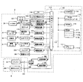
図15は、本実施形態のタグラベル作成装置1の制御系を表す機能ブロック図である。図15において、このタグラベル作成装置1の制御基板(図示せず)上には、制御回路110(情報生成手段)が配置されている。   FIG. 15 is a functional block diagram showing a control system of the tag label producing apparatus 1 of the present embodiment. In FIG. 15, a control circuit 110 (information generating means) is arranged on a control board (not shown) of the tag label producing apparatus 1.

制御回路110には、内部にタイマ111Aを備え各機器を制御するCPU111と、このCPU111にデータバス112を介して接続された入出力インターフェース113と、CGROM114と、ROM115,116と、RAM117とが設けられている。   The control circuit 110 includes a CPU 111 having an internal timer 111A for controlling each device, an input / output interface 113 connected to the CPU 111 via a data bus 112, a CGROM 114, ROMs 115 and 116, and a RAM 117. It has been.

CGROM114には、多数のキャラクタの各々に関して、表示のためのドットパターンデータがコードデータに対応させて格納されている。   The CGROM 114 stores dot pattern data for display corresponding to the code data for each of a large number of characters.

ROM(ドットパターンデータメモリ)115には、アルファベット文字や記号等のキャラクタを印字するための多数のキャラクタ各々に関して、印字用ドットパターンデータが、書体(ゴシック系書体、明朝体書体等)毎に分類され、各書体毎に印字文字サイズ分、コードデータに対応させて格納されている。また、階調表現を含むグラフィック画像を印字するためのグラフィックパターンデータも記憶されている。   In a ROM (dot pattern data memory) 115, for each of a large number of characters for printing characters such as alphabet letters and symbols, printing dot pattern data is provided for each typeface (Gothic typeface, Mincho typeface, etc.). Each typeface is classified and stored in correspondence with the code data for the print character size. In addition, graphic pattern data for printing a graphic image including gradation expression is also stored.

ROM116には、上記PC118から入力された文字や数字等のキャラクタのコードデータに対応させて、印字バッファのデータを読み出して上記印字ヘッド23、搬送用モータ119、テープ排出モータ65を駆動する印字駆動制御プログラム、各印字ドットの形成エネルギ量に対応するパルス数を決定するパルス数決定プログラム、印字終了した場合に印字済みタグラベル用テープ109を切断位置まで搬送用モータ119を駆動して搬送し、上記カッターモータ43を駆動して印字済みタグラベル用テープ109を切断する切断駆動制御プログラム、切断された印字済みタグラベル用テープ109(=無線タグラベルT)をテープ排出モータ65を駆動してラベル排出口11から強制的に排出するテープ排出プログラム、その他タグラベル作成装置1の制御上必要な各種のプログラムが格納されている。CPU111は、このようなROM116に記憶されている各種プログラムに基づいて各種の演算を行う。   The ROM 116 reads the print buffer data in correspondence with the character code data such as characters and numbers input from the PC 118 and drives the print head 23, the transport motor 119, and the tape discharge motor 65. A control program, a pulse number determination program for determining the number of pulses corresponding to the amount of energy to form each print dot, and when printing is finished, the tag label tape 109 with print is transported by driving the transport motor 119 to the cutting position. A cutting drive control program for driving the cutter motor 43 to cut the tag label tape 109 with print, and the cut tag label tape 109 with print (= the RFID label T) from the label discharge port 11 by driving the tape discharge motor 65. Forcible tape ejection program and other tags Bell generating apparatus 1 controls various programs required for are stored. The CPU 111 performs various calculations based on various programs stored in the ROM 116.

RAM117には、テキストメモリ117A、印字バッファ117B、パラメータ記憶エリア117E等が設けられている。テキストメモリ117Aには、PC118から入力された文書データが格納される。印字バッファ117Bには、複数の文字や記号等の印字用ドットパターンや各ドットの形成エネルギ量である印加パルス数等がドットパターンデータとして格納され、印字ヘッド23はこの印字バッファ117Bに記憶されているドットパターンデータに従ってドット印字を行う。パラメータ記憶エリア117Eには、各種演算データが記憶される。   The RAM 117 is provided with a text memory 117A, a print buffer 117B, a parameter storage area 117E, and the like. The text memory 117A stores document data input from the PC 118. In the print buffer 117B, a dot pattern for printing such as a plurality of characters and symbols, the number of applied pulses that is the amount of energy for forming each dot, and the like are stored as dot pattern data. The print head 23 is stored in the print buffer 117B. Dot printing is performed according to the existing dot pattern data. Various calculation data are stored in the parameter storage area 117E.

入出力インターフェース113には、PC118と、印字ヘッド23を駆動するための上記印刷駆動回路120と、搬送用モータ119を駆動するための搬送用モータ駆動回路121と、カッターモータ43を駆動するためのカッターモータ駆動回路122と、ハーフカッタモータ129を駆動するためのハーフカッタモータ駆動回路128と、テープ排出モータ65を駆動するためのテープ排出モータ駆動回路123と、上記ソレノイド210を駆動するためのソレノイド駆動回路215と、識別マークPMを検出する上記マークセンサ127と、テープカットセンサ124と、カットリリース検出センサ125と、アンテナユニット9が装置本体2に装着されているかどうかを検出する装着センサ301と、アンテナユニット9内のループアンテナLCを介して無線タグ回路素子Toと情報の送受信を行うための送信回路306及び受信回路307と、アンテナユニット9に設けられた上記操作スイッチ302とが各々接続されている。   The input / output interface 113 includes a PC 118, the print drive circuit 120 for driving the print head 23, a transport motor drive circuit 121 for driving the transport motor 119, and a cutter motor 43. A cutter motor drive circuit 122, a half cutter motor drive circuit 128 for driving the half cutter motor 129, a tape discharge motor drive circuit 123 for driving the tape discharge motor 65, and a solenoid for driving the solenoid 210 A drive circuit 215, the mark sensor 127 for detecting the identification mark PM, a tape cut sensor 124, a cut release detection sensor 125, and a mounting sensor 301 for detecting whether the antenna unit 9 is mounted on the apparatus main body 2; The loop in the antenna unit 9 A transmitting circuit 306 and receiving circuit 307 for transmitting and receiving wireless tag circuit element To and the information via the antenna LC, and the operation switch 302 provided in the antenna unit 9 are respectively connected.

上記送信回路306及び受信回路307は、アンテナ共用器240を介してループアンテナLCに接続されている。これにより、1つのループアンテナLCを用いて信号の送信及び受信が可能となっている。また、アンテナユニット9側のループアンテナLCと装置本体2側の上記アンテナ共用器240をそれぞれ接続する配線、アンテナユニット9側の操作スイッチ302と装置本体2側の入出力インターフェース113を接続する配線等が束ねられて上記ケーブル223を構成している。   The transmission circuit 306 and the reception circuit 307 are connected to the loop antenna LC via the antenna duplexer 240. Thereby, signal transmission and reception are possible using one loop antenna LC. Further, wiring for connecting the loop antenna LC on the antenna unit 9 side and the antenna duplexer 240 on the apparatus body 2 side, wiring for connecting the operation switch 302 on the antenna unit 9 side and the input / output interface 113 on the apparatus body 2 side, etc. Are bundled to form the cable 223.

上記装着センサ301(検出手段)は、装置本体2の係合部201に設けられたいわゆるリミットスイッチであり、アンテナユニット9が装置本体2に装着されるとONとなり、その検出信号を制御回路110に出力するようになっている。そして、制御回路110は、装着センサ301から検出信号が入力された場合はタグラベル作成のための書き込みモードに切換え、装着センサ301からの検出信号が入力されない場合はタグラベル作成装置1をリーダとして機能させる読み取りモードに切換えるようになっている。   The mounting sensor 301 (detection means) is a so-called limit switch provided in the engaging portion 201 of the apparatus main body 2, and is turned on when the antenna unit 9 is mounted on the apparatus main body 2, and the detection signal is sent to the control circuit 110. To output. When the detection signal is input from the mounting sensor 301, the control circuit 110 switches to the writing mode for creating the tag label, and when the detection signal from the mounting sensor 301 is not input, the control circuit 110 functions as the reader. Switch to reading mode.

なお、ここでは装着センサとしてリミットスイッチを用いたが、これに限られず、例えば装置本体2とアンテナユニット9とをコネクタ接続とし、当該コネクタの端子同士が接続され導通されたときに流れる電流を検出することにより、装置本体2とアンテナユニット9との装着状態を検出するようにしてもよい。また、アンテナユニット9の装置本体2への装着時に閉成されるマイクロスイッチ等を用いてもよい。   In this case, the limit switch is used as the mounting sensor. However, the present invention is not limited to this. For example, the apparatus main body 2 and the antenna unit 9 are connected to a connector, and a current flowing when the terminals of the connector are connected and connected is detected. By doing so, the mounting state of the apparatus main body 2 and the antenna unit 9 may be detected. Further, a micro switch or the like that is closed when the antenna unit 9 is attached to the apparatus main body 2 may be used.

そして、例えば上記書き込みモードの際にPC118を介して文字データ等が入力されると、そのテキスト(文書データ)がテキストメモリ117Aに順次記憶されるとともに、印字ヘッド23が駆動回路120を介して駆動され、各発熱素子が1ライン分の印字ドットに対応して選択的に発熱駆動されて印字バッファ117Bに記憶されたドットパターンデータの印字を行い、これと同期して搬送用モータ119が駆動回路121を介してテープの搬送制御を行う。また、送信回路306が制御回路110からの制御信号に基づき搬送波の変調制御を行うとともに、受信回路307は制御回路110からの制御信号に基づき復調した信号の処理を行う。   For example, when character data or the like is input via the PC 118 in the writing mode, the text (document data) is sequentially stored in the text memory 117A and the print head 23 is driven via the drive circuit 120. Each heating element is selectively driven to generate heat corresponding to the printing dots for one line and prints the dot pattern data stored in the print buffer 117B. In synchronization with this, the transport motor 119 drives the drive circuit. Control of tape conveyance is performed via 121. In addition, the transmission circuit 306 performs carrier wave modulation control based on the control signal from the control circuit 110, and the reception circuit 307 processes the demodulated signal based on the control signal from the control circuit 110.

また、テープカットセンサ124及びカットリリース検出センサ125は、カッターハスバギヤ42の円筒外壁上に設けられたカッターハスバギヤ用カム42Aとマイクロスイッチ126とから構成されている(図8、図9等参照)。具体的には、カッターモータ43によりカッターハスバギヤ42が回転すると、カッターハスバギヤ用カム42Aの作用によりマイクロスイッチ126がオフ状態からオン状態に切り替わり、可動刃45による印字済みタグラベル用テープ109の切断が完了したことを検出する。このことにより、テープカットセンサ124が構成される。また、更にカッターハスバギヤ42が回転すると、カッターハスバギヤ用カム42Aの作用によりマイクロスイッチ126がオン状態からオフ状態に切り替わり、可動刃45がリリース位置に戻ったことを検出する。このことにより、カットリリース検出センサ125が構成される。   Further, the tape cut sensor 124 and the cut release detection sensor 125 are constituted by a cutter helical gear cam 42A provided on the cylindrical outer wall of the cutter helical gear 42 and a micro switch 126 (see FIGS. 8 and 9). ). Specifically, when the cutter helical gear 42 is rotated by the cutter motor 43, the micro switch 126 is switched from the OFF state to the ON state by the action of the cutter helical gear cam 42A, and the tag label tape 109 with print is cut by the movable blade 45. Detect that is complete. Thus, the tape cut sensor 124 is configured. When the cutter helical gear 42 further rotates, the micro switch 126 is switched from the on state to the off state by the action of the cutter helical gear cam 42A, and it is detected that the movable blade 45 has returned to the release position. Thus, the cut release detection sensor 125 is configured.

図16は、上記無線タグ回路素子Toの機能的構成を表す機能ブロック図である。この図16において、無線タグ回路素子Toは、タグラベル作成装置1側のループアンテナLCと磁気誘導により非接触で信号の送受信を行う上記ループアンテナ152と、このループアンテナ152に接続された上記IC回路部151とを有している。   FIG. 16 is a functional block diagram showing a functional configuration of the RFID circuit element To. In FIG. 16, the RFID circuit element To includes the loop antenna 152 that performs contactless transmission / reception of signals with the loop antenna LC on the tag label producing apparatus 1 side, and the IC circuit connected to the loop antenna 152. Part 151.

IC回路部151は、ループアンテナ152により受信された搬送波を整流する整流部153と、この整流部153により整流された搬送波のエネルギを蓄積し駆動電源とするための電源部154と、上記ループアンテナ152により受信された搬送波からクロック信号を抽出して制御部155に供給するクロック抽出部156と、所定の情報信号を記憶し得るメモリ部157と、上記ループアンテナ152に接続された変復調部158と、上記整流部153、クロック抽出部156、及び変復調部158等を介して上記無線タグ回路素子Toの作動を制御するための上記制御部155とを備えている。   The IC circuit unit 151 includes a rectifying unit 153 that rectifies the carrier wave received by the loop antenna 152, a power source unit 154 that accumulates energy of the carrier wave rectified by the rectifying unit 153 and uses it as a driving power source, and the loop antenna. 152, a clock extraction unit 156 that extracts a clock signal from the carrier wave received by 152 and supplies the clock signal to the control unit 155, a memory unit 157 that can store a predetermined information signal, and a modulation / demodulation unit 158 connected to the loop antenna 152 And a control unit 155 for controlling the operation of the RFID circuit element To through the rectifying unit 153, the clock extracting unit 156, the modem unit 158, and the like.

変復調部158は、ループアンテナ152により受信された上記タグラベル作成装置1のループアンテナLCからの通信信号の復調を行うと共に、上記制御部155からの応答信号に基づき、ループアンテナ152より受信された搬送波を変調反射する。   The modulation / demodulation unit 158 demodulates the communication signal received from the loop antenna 152 from the loop antenna LC of the tag label producing apparatus 1 and receives the carrier wave received from the loop antenna 152 based on the response signal from the control unit 155. Modulate and reflect.

制御部155は、上記変復調部158により復調された受信信号を解釈し、上記メモリ部157において記憶された情報信号に基づいて返信信号を生成し、上記変復調部158により返信する制御等の基本的な制御を実行する。   The control unit 155 interprets the received signal demodulated by the modulation / demodulation unit 158, generates a return signal based on the information signal stored in the memory unit 157, and performs basic control such as returning by the modulation / demodulation unit 158. Execute proper control.

図17(a)及び図17(b)は、上述のような構成であるタグラベル作成装置1により無線タグ回路素子Toの情報書き込み(又は読み取り)及び印字済タグラベル用テープ109の切断が完了し形成された無線タグラベルTの外観の一例を表す図であり、図17(a)は上面図、図17(b)は下面図である。また図18(a)は図17中XVIIIA−XVIIIA′断面による横断面図を反時計方向に90°回転させた図であり、図18(b)は図17中XVIIIB−XVIIIB′断面による横断面図を反時計方向に90°回転させた図である。   17 (a) and 17 (b) are formed when the tag label producing apparatus 1 having the above-described configuration completes the writing (or reading) of information on the RFID circuit element To and the cutting of the tag label tape 109 with print. It is a figure showing an example of the external appearance of the made RFID label T, FIG.17 (a) is a top view, FIG.17 (b) is a bottom view. 18A is a view obtained by rotating the transverse cross section taken along the XVIIIA-XVIIIA ′ cross section in FIG. 17 by 90 ° counterclockwise, and FIG. 18B is the cross section taken along the XVIIIB-XVIIIB ′ cross section in FIG. It is the figure which rotated the figure 90 degrees counterclockwise.

これら図17(a)、図17(b)、図18(a)、及び図18(b)において、無線タグラベルTは、前述したように図5に示した4層構造にカバーフィルム103が加わった5層構造となっており、カバーフィルム103側(図18中上側)よりその反対側(図18中下側)へ向かって、カバーフィルム103、粘着層101a、ベースフィルム101b、粘着層101c、剥離紙101dで5層を構成している。そして、前述のようにベースフィルム101bの裏側に設けられたループアンテナ152を含む無線タグ回路素子Toがベースフィルム101b及び粘着層101c内に備えられるとともに、カバーフィルム103の裏面に無線タグ回路素子Toの記憶情報等に対応したラベル印字R(この例では無線タグラベルTの種類を示す「RF−ID」の文字)が印刷されている。   17 (a), 17 (b), 18 (a), and 18 (b), the RFID label T has a cover film 103 added to the four-layer structure shown in FIG. 5 as described above. The cover film 103, the adhesive layer 101a, the base film 101b, the adhesive layer 101c, from the cover film 103 side (upper side in FIG. 18) to the opposite side (lower side in FIG. 18) The release paper 101d constitutes 5 layers. As described above, the RFID circuit element To including the loop antenna 152 provided on the back side of the base film 101b is provided in the base film 101b and the adhesive layer 101c, and the RFID circuit element To is provided on the back surface of the cover film 103. A label print R (in this example, “RF-ID” indicating the type of the RFID label T) corresponding to the stored information is printed.

また、カバーフィルム103、粘着層101a、ベースフィルム101b、粘着層101cには、既に述べたように上記ハーフカッタ34によってテープ幅方向に略沿ってハーフカット線HC(半切断部位。但しこの例では前ハーフカット線HC1及び後ハーフカット線HC2の2本。)が形成されている。カバーフィルム103のうち、これらハーフカット線HC1,HC2の間に挟まれた領域がラベル印字Rが印刷される印字領域Sとなり、印字領域Sよりハーフカット線HC1,HC2を挟んでテープ長手方向両側がそれぞれ前余白領域S1及び後余白領域S2となっている。言い換えれば、ハーフカット線HC1,HC2により、カバーフィルム103の前後余白領域S1,S2と印字領域Sとが区別されている。   Also, the cover film 103, the adhesive layer 101a, the base film 101b, and the adhesive layer 101c are provided with the half-cut line HC (half-cut portion. However, in this example, substantially along the tape width direction by the half cutter 34 as described above. The front half-cut line HC1 and the rear half-cut line HC2 are formed. In the cover film 103, an area sandwiched between the half-cut lines HC1 and HC2 is a print area S on which the label print R is printed, and both sides in the longitudinal direction of the tape sandwiching the half-cut lines HC1 and HC2 from the print area S Are a front margin area S1 and a rear margin area S2. In other words, the front and rear margin areas S1, S2 and the print area S of the cover film 103 are distinguished by the half-cut lines HC1, HC2.

なお、既に述べたように識別マークPMとして図18(a)及び図18(b)に示すような黒塗りのマーキングを設けるのに代え、図18(c)に示すように、識別マークPMとして、トムソン型やビク型による打ち抜きやレーザ加工等により基材テープ101を略貫通する孔を孔設する等でもよい。この場合、マークセンサ127を投光器及び受光器からなる反射型の公知の光電センサで構成した場合、投光器と受光器との間の位置に上記孔からなる識別マークPMが来ると、投光器からの光が識別マークPMの孔及び透明のカバーフィルム103を透過して反射しなくなって受光器で受光しなくなり、これによって受光器からの制御出力が反転させられる。   As already described, instead of providing the black marking as shown in FIG. 18A and FIG. 18B as the identification mark PM, as shown in FIG. Alternatively, a hole substantially penetrating the base tape 101 may be provided by punching with a Thomson type or a Bic type, laser processing, or the like. In this case, when the mark sensor 127 is constituted by a known reflection type photoelectric sensor composed of a projector and a light receiver, if the identification mark PM composed of the hole comes at a position between the light projector and the light receiver, the light from the light projector Is transmitted through the hole of the identification mark PM and the transparent cover film 103 and is not reflected and is not received by the light receiver, thereby inverting the control output from the light receiver.

図19は、上述したようなタグラベル作成装置1による無線タグ回路素子ToのIC回路部151の無線タグ情報へのアクセス(読み取り又は書き込み)に際して、上記PC118(端末118a又は汎用コンピュータ118b)に表示される画面の一例を表す図である。   FIG. 19 is displayed on the PC 118 (terminal 118a or general-purpose computer 118b) when accessing (reading or writing) the RFID tag information of the IC circuit unit 151 of the RFID circuit element To by the tag label producing apparatus 1 as described above. It is a figure showing an example of a screen.

図19において、この例では、タグラベルの種別(アクセス周波数及びテープ寸法)、無線タグ回路素子Toに対応して印刷された印字文字R、その無線タグ回路素子Toに固有の識別情報(タグID)であるアクセス(読み取り又は書き込み)ID、上記情報サーバISに記憶された物品情報のアドレス、及び上記ルートサーバRSにおけるそれらの対応情報の格納先アドレス等が上記PC118に表示可能となっている。そして、そのPC118の操作によりタグタグラベル作成装置1が作動されて、カバーフィルム103に上記印字文字Rが印刷されると共に、IC回路部151に上記書き込みIDや物品情報等の情報が書き込まれる(又はIC回路部151に予め記憶された読み取りIDや物品情報等の情報が読みとられる)。   In FIG. 19, in this example, the type of tag label (access frequency and tape size), the printed character R printed corresponding to the RFID circuit element To, and identification information (tag ID) unique to the RFID circuit element To The access (read or write) ID, the address of the article information stored in the information server IS, the storage address of the corresponding information in the route server RS, and the like can be displayed on the PC 118. Then, the tag tag label producing apparatus 1 is operated by the operation of the PC 118, the print character R is printed on the cover film 103, and information such as the write ID and article information is written on the IC circuit unit 151 (or Information such as read ID and article information stored in advance in the IC circuit unit 151 is read).

なお、上記のような読み取り又は書き込みの際、生成された無線タグラベルTの無線タグ回路素子ToのタグIDとその無線タグラベルTのIC回路部151から読みとられた情報(又はIC回路部151に書き込まれた情報)との対応関係は、前述のルートサーバRSに記憶され、必要に応じて参照できるようになっている。   At the time of reading or writing as described above, the tag ID of the RFID tag circuit element To of the generated RFID label T and information read from the IC circuit portion 151 of the RFID label T (or to the IC circuit portion 151) The correspondence relationship with the (written information) is stored in the above-described route server RS and can be referred to as necessary.

上記のような基本構成のタグラベル作成装置1では、アンテナユニット9の装着状態(すなわち、上記書き込みモード)において、貼り合わされて生成された印字済みタグラベル用テープ109に対しループアンテナLCにより無線タグ回路素子Toに情報読み取り又は書き込みが行われた後、切断機構15によって印字済みタグラベル用テープ109が切断されて無線タグラベルTが生成される。   In the tag label producing apparatus 1 having the basic configuration as described above, when the antenna unit 9 is mounted (that is, in the writing mode), the RFID tag circuit element is attached to the tag label tape 109 with print generated by being bonded together by the loop antenna LC. After information reading or writing is performed on To, the tag label tape 109 with print is cut by the cutting mechanism 15 to generate the RFID label T.

図20は、上記制御回路110によって実行される制御手順を表すフローチャートである。このフローは、例えばタグラベル作成装置1の電源が投入されたときに開始される。   FIG. 20 is a flowchart showing a control procedure executed by the control circuit 110. This flow is started when the power of the tag label producing apparatus 1 is turned on, for example.

この図20において、まずステップS1で、装着センサ301からの検出信号に基づき、センサユニット9が装置本体2に装着されているかどうかを判定する。アンテナユニット9が装置本体2に装着されている場合(言い換えれば、装着センサ301からの検出信号が入力されている場合)、ステップS1の判定が満たされ、ステップS100の書き込みモードに移る。なお、ここでいう書き込みモードとは、タグラベル作成装置1で無線タグラベルTを作成する動作モードのことであり、無線タグ回路素子Toに対し無線タグ情報を送信しIC回路部151に書き込みを行って無線タグラベルTを作成する場合(後述の図23参照)と、予め所定の無線タグ情報が書き換え不可に記憶保持されている読み取り専用の無線タグ回路素子Toから無線タグ情報を読み取りながら、これに対応する印字を行って無線タグラベルTを作成する場合も含むものである。一方、アンテナユニット9が装置本体2から取り外されている場合(言い換えれば、装着センサ301からの検出信号が入力されていない場合)、ステップS1の判定が満たされず、ステップS300の読み取りモードに移る。この読み取りモードとは、タグラベル作成装置1を、作成装置外の無線タグラベル(無線タグ回路素子To)から無線タグ情報を読み取るリーダとして用いる動作モードである。   In FIG. 20, first, in step S <b> 1, based on the detection signal from the mounting sensor 301, it is determined whether or not the sensor unit 9 is mounted on the apparatus main body 2. When the antenna unit 9 is attached to the apparatus main body 2 (in other words, when a detection signal from the attachment sensor 301 is input), the determination in step S1 is satisfied, and the writing mode in step S100 is entered. Note that the writing mode here is an operation mode in which the RFID label producing device 1 creates the RFID label T. The RFID tag information is transmitted to the RFID circuit element To and written to the IC circuit unit 151. Corresponding to the case where the RFID label T is created (see FIG. 23 described later), while reading the RFID tag information from the read-only RFID circuit element To in which predetermined RFID tag information is stored and retained in a non-rewritable manner in advance. This includes the case where the RFID label T is created by performing printing. On the other hand, when the antenna unit 9 is removed from the apparatus main body 2 (in other words, when the detection signal from the mounting sensor 301 is not input), the determination at Step S1 is not satisfied, and the process proceeds to the reading mode at Step S300. The reading mode is an operation mode in which the tag label producing apparatus 1 is used as a reader for reading the RFID tag information from the RFID label (RFID circuit element To) outside the producing apparatus.

図21は、タグラベル作成時に制御回路110によって実行される制御手順を表すフローチャートである。この図21において、上述したステップS100の書き込みモードとなっている状態で、例えば上記PC118を介しタグラベル作成装置1による所定の無線タグラベル作成の開始操作が行われると、このフローが開始される。   FIG. 21 is a flowchart showing a control procedure executed by the control circuit 110 when creating a tag label. In FIG. 21, when a predetermined RFID label production start operation is performed by the tag label production apparatus 1 through the PC 118 in the state where the writing mode in step S100 described above is set, for example, this flow is started.

まずステップS105で、上記PC118を介しタグラベル作成装置1による所定の無線タグラベル作成の開始操作が行われると、PC118からの操作信号に基づき印刷データや無線タグ回路素子Toとの通信データ、前・後ハーフカット位置やフルカット位置の設定等を行なう準備処理を実行する。   First, in step S105, when a predetermined RFID label production start operation is performed by the tag label producing apparatus 1 via the PC 118, print data, communication data with the RFID circuit element To, based on an operation signal from the PC 118, front and rear Preparation processing for setting the half-cut position and full-cut position is executed.

次に、ステップS108において、送信回路306に制御信号を出力してループアンテナLCの送信出力が予め定められた小さな出力値となるように設定し、その後、ステップS110において、ループアンテナLCから無線タグ回路素子Toへ通信を行う際、無線タグ回路素子Toからの応答がない場合に通信再試行(リトライ)を行う回数(アクセス試行回数)をカウントする変数M、Nと、通信が成功したかどうかをあらわすフラグFを0に初期化設定する。なお、上記予め定められた小さな出力値は、送信出力が大きすぎるとカートリッジ7内、又は作成済みの無線タグラベルTの無線タグ回路素子Toとの不要な通信がなされることから、そのようなことが起こらないように予め実験・計算等によって定められた、搬送される無線タグ回路素子Toとの通信に最適な出力値に設定されている。   Next, in step S108, a control signal is output to the transmission circuit 306 to set the transmission output of the loop antenna LC to a predetermined small output value, and then, in step S110, the wireless tag from the loop antenna LC is set. When communicating with the circuit element To, when there is no response from the RFID circuit element To, variables M and N for counting the number of times of communication retry (retry) (number of access attempts) and whether the communication is successful Is initialized to 0. The predetermined small output value is such that if the transmission output is too large, unnecessary communication with the RFID circuit element To of the RFID label T that has already been created or the RFID label T is made. The output value is set to an optimum output value for communication with the RFID circuit element To to be transported, which is determined in advance by experiments and calculations so as not to occur.

その後、ステップS115に移り、入出力インターフェース113を介し搬送用モータ駆動回路121に制御信号を出力し、搬送用モータ121の駆動力によってテープ送りローラ27及びリボン巻取りローラ106を回転駆動させる。さらに、テープ排出モータ駆動回路123を介してテープ排出モータ65に制御信号を出力し、駆動ローラ51を回転駆動させる。これらにより、第1ロール102から基材テープ101が繰り出されテープ送りローラ27へ供給されるとともに、第2ロール104からはカバーフィルム103が繰り出され、これら基材テープ101とカバーフィルム103とが上記テープ送りローラ27及びサブローラ109により接着されて一体化されて印字済タグラベル用テープ109として形成され、カートリッジ7外方向からさらにタグラベル作成装置1外方向へと搬送される。   Thereafter, the process proceeds to step S115, where a control signal is output to the conveying motor drive circuit 121 via the input / output interface 113, and the tape feeding roller 27 and the ribbon take-up roller 106 are driven to rotate by the driving force of the conveying motor 121. Further, a control signal is output to the tape discharge motor 65 via the tape discharge motor drive circuit 123 to drive the drive roller 51 to rotate. Accordingly, the base tape 101 is fed out from the first roll 102 and supplied to the tape feed roller 27, and the cover film 103 is fed out from the second roll 104. The base tape 101 and the cover film 103 are The tape label roller 109 and the sub-roller 109 are bonded and integrated to form a tag label tape 109 with print, which is further conveyed from the outside of the cartridge 7 to the outside of the tag label producing apparatus 1.

その後、ステップS120において、入出力インターフェース113を介し入力されたマーク検出センサ127の検出信号に基づき、基材テープ101の上記識別子PMが検出されたかどうか(言い換えればカバーフィルム103が印字ヘッド23による印刷開始位置まで到達したかどうか)を判定する。識別子PMが検出されるまで判定が満たされずこの手順を繰り返し、検出されたら判定が満たされて次のステップS125に移る。   Thereafter, whether or not the identifier PM of the base tape 101 is detected based on the detection signal of the mark detection sensor 127 input via the input / output interface 113 in step S120 (in other words, the cover film 103 is printed by the print head 23). Whether the start position has been reached). The determination is not satisfied until the identifier PM is detected, and this procedure is repeated. When the identifier PM is detected, the determination is satisfied and the process proceeds to the next step S125.

ステップS125では、入出力インターフェース113を介し印刷駆動回路120に制御信号を出力し、印字ヘッド23を通電して、カバーフィルム103のうち前述した印字領域S(=基材テープ101に所定ピッチで等間隔で配置された無線タグ回路素子Toの裏面にほぼ貼り合わせることとなる領域)に、ステップS105で生成した印刷データに対応した文字、記号、バーコード等のラベル印字Rの印刷を開始する。   In step S125, a control signal is output to the print drive circuit 120 via the input / output interface 113, the print head 23 is energized, and the above-described print region S of the cover film 103 (= the base tape 101 at a predetermined pitch or the like). Printing of label print R such as characters, symbols, barcodes, etc. corresponding to the print data generated in step S105 is started on the back surface of the RFID circuit element To arranged at intervals.

その後、ステップS130において、印字済タグラベル用テープ109が先のステップS105で設定した前ハーフカット位置まで搬送されたかどうか(言い換えればハーフカット機構35のハーフカッタ34がステップS1で設定した前ハーフカット線HC1に正対する位置まで印字済みタグラベル用テープ109が到達したかどうか)を判定する。このときの判定は、例えば、上記ステップS120において基材テープ101の識別子PMを検出した後の搬送距離を所定の公知の方法で検出すればよい(パルスモータである搬送用モータ119を駆動する搬送用モータ駆動回路121の出力するパルス数をカウントする等)。前ハーフカット位置に到達するまで判定が満たされずこの手順を繰り返し、到達したら判定が満たされて次のステップS135に移る。   Thereafter, in step S130, whether or not the tag label tape 109 with print has been transported to the previous half-cut position set in the previous step S105 (in other words, the half-cut line set by the half cutter 34 of the half-cut mechanism 35 in step S1). It is determined whether the tag label tape 109 with print has reached a position directly facing HC1. The determination at this time may be performed, for example, by detecting a transport distance after detecting the identifier PM of the base tape 101 in the above-described step S120 (transport that drives the transport motor 119 that is a pulse motor). The number of pulses output from the motor drive circuit 121 is counted). The determination is not satisfied until the previous half-cut position is reached, and this procedure is repeated. When the previous half-cut position is reached, the determination is satisfied and the routine goes to the next Step S135.

ステップS135では、入出力インターフェース113を介し搬送用モータ駆動回路121及びテープ排出モータ駆動回路123に制御信号を出力し、搬送用モータ119及びテープ排出モータ65の駆動を停止して、テープ送りローラ27、リボン巻取りローラ106、駆動ローラ51の回転を停止する。これにより、カートリッジ7から繰り出された印字済タグラベル用テープ109が排出方向に移動する過程で、ステップS105で設定した前ハーフカット線HC1にハーフカット機構35のハーフカッタ34が正対した状態で、第1ロール102からの基材テープ101の繰り出し、第2ロール104からのカバーフィルム103の繰り出し、及び印字済みタグラベル用テープ109の搬送が停止する。またこのとき、入出力インターフェース113を介し印刷駆動回路120にも制御信号を出力し、印字ヘッド23の通電を停止して、上記ラベル印字Rの印刷を停止(印刷中断)する。   In step S135, control signals are output to the transport motor drive circuit 121 and the tape discharge motor drive circuit 123 via the input / output interface 113, the drive of the transport motor 119 and the tape discharge motor 65 is stopped, and the tape feed roller 27 is output. Then, the rotation of the ribbon take-up roller 106 and the driving roller 51 is stopped. Thus, in the process in which the tag label tape 109 with print fed out from the cartridge 7 moves in the discharge direction, the half cutter 34 of the half cut mechanism 35 faces the front half cut line HC1 set in step S105. The feeding of the base tape 101 from the first roll 102, the feeding of the cover film 103 from the second roll 104, and the conveyance of the tag label tape 109 with print are stopped. At this time, a control signal is also output to the print drive circuit 120 via the input / output interface 113, the energization of the print head 23 is stopped, and printing of the label print R is stopped (print interruption).

その後、ステップS140で、入出力インターフェース113を介しハーフカッタモータ駆動回路128に制御信号を出力してハーフカッタモータ129を駆動し、ハーフカッタ34を回動させて、印字済タグラベル用テープ109のカバーフィルム103、粘着層101a、ベースフィルム101b、及び粘着層101cを切断して前ハーフカット線HC1を形成する前ハーフカット処理を行う。   Thereafter, in step S140, a control signal is output to the half cutter motor drive circuit 128 via the input / output interface 113 to drive the half cutter motor 129 and rotate the half cutter 34 to cover the tag tag tape 109 with print. A pre-half-cut process for cutting the film 103, the adhesive layer 101a, the base film 101b, and the adhesive layer 101c to form the front half-cut line HC1 is performed.

そして、ステップS145に移り、上記ステップS115と同様にしてテープ送りローラ27、リボン巻取りローラ106、駆動ローラ51を回転駆動させて印字済タグラベル用テープ109の搬送を再開するとともに、ステップS125と同様にして印字ヘッド23に通電してラベル印字Rの印刷を再開する。   Then, the process proceeds to step S145, and similarly to step S115, the tape feeding roller 27, the ribbon take-up roller 106, and the driving roller 51 are rotationally driven to resume the transport of the tag label tape 109 with print, and the same as step S125. Then, the print head 23 is energized to resume the printing of the label print R.

その後、ステップS150において、搬送される印字済タグラベル用テープ109が所定値(例えば、対応する印字が施されたカバーフィルム103が貼り合わされた無線タグ回路素子Toが上記ループアンテナLCに到達するだけの搬送距離)だけ搬送されたかどうかを判断する。このときの搬送距離判定も、上記ステップS130と同様に、パルスモータである搬送用モータ119を駆動する搬送用モータ駆動回路121の出力するパルス数をカウントする等により行えば足りる。   After that, in step S150, the tag label tape 109 to be conveyed has a predetermined value (for example, the RFID circuit element To to which the cover film 103 on which the corresponding printing has been applied is pasted only reaches the loop antenna LC. It is determined whether or not it has been transported by (transport distance). Similar to step S130, the conveyance distance at this time may be determined by counting the number of pulses output from the conveyance motor drive circuit 121 that drives the conveyance motor 119, which is a pulse motor.

次のステップS200では、タグアクセス処理を行う。すなわち、無線タグ回路素子Toの通信位置(無線タグ回路素子ToがループアンテナLCと正対する位置)まで搬送したら搬送及び印字を停止して情報送受信を行い、その後搬送及び印字を再開して印字を完了させ、さらに搬送して後ハーフカット位置で搬送を停止して後ハーフカット線HC2の形成を行う(後述の図22参照)。   In the next step S200, tag access processing is performed. That is, when the RFID tag circuit element To is conveyed to the communication position (the position where the RFID tag circuit element To faces the loop antenna LC), the conveyance and printing are stopped, information is transmitted and received, and then the conveyance and printing are resumed to perform printing. After completion of the transfer, the transfer is stopped at the rear half-cut position, and the rear half-cut line HC2 is formed (see FIG. 22 described later).

以上のようにしてステップS200が終了したら、ステップS155に移る(なおこの時点でステップS200において印字済みタグラベル用テープ109の搬送が再開されている)。ステップS155では、印字済タグラベル用テープ109が前述したフルカット位置まで搬送されたかどうか(言い換えれば切断機構15の可動刃41がステップS1で設定した切断線CLに正対する位置まで印字済みタグラベル用テープ109が到達したかどうか)を判定する。このときの判定も、前述と同様、例えば、上記ステップS120において基材テープ101の識別子PMを検出した後の搬送距離を所定の公知の方法で検出すればよい(パルスモータである搬送用モータ119を駆動する搬送用モータ駆動回路121の出力するパルス数をカウントする等)。フルカット位置に到達するまで判定が満たされずこの手順を繰り返し、到達したら判定が満たされて次のステップS160に移る。   When step S200 is completed as described above, the process proceeds to step S155 (at this time, the transport of the tag label tape 109 with print has been resumed in step S200). In step S155, whether or not the tag label tape 109 with print has been transported to the above-described full cut position (in other words, the tag label tape with print until the position where the movable blade 41 of the cutting mechanism 15 faces the cutting line CL set in step S1). 109) is determined. The determination at this time may be performed in the same manner as described above, for example, by detecting the transport distance after detecting the identifier PM of the base tape 101 in step S120 (a transport motor 119 which is a pulse motor). The number of pulses output from the conveyance motor drive circuit 121 that drives the motor is counted, etc.). The determination is not satisfied until the full cut position is reached, and this procedure is repeated. When the full cut position is reached, the determination is satisfied, and the process proceeds to the next step S160.

ステップS160では、上記ステップS135と同様にして、テープ送りローラ27、リボン巻取りローラ106、駆動ローラ51の回転を停止して印字済タグラベル用テープ109の搬送を停止する。これにより、ステップS105で設定した切断線CLに切断機構15の可動刃41が正対した状態で、第1ロール102からの基材テープ101の繰り出し、第2ロール104からのカバーフィルム103の繰り出し、及び印字済みタグラベル用テープ109の搬送が停止する。   In step S160, similarly to step S135, the rotation of the tape feeding roller 27, the ribbon take-up roller 106, and the driving roller 51 is stopped, and the conveyance of the tag label tape 109 with print is stopped. Thus, the base tape 101 is fed from the first roll 102 and the cover film 103 is fed from the second roll 104 with the movable blade 41 of the cutting mechanism 15 facing the cutting line CL set in step S105. , And the transport of the tag label tape 109 with print is stopped.

その後、ステップS165でカッタモータ駆動回路122に制御信号を出力してカッターモータ43を駆動し、切断機構15の可動刃41を回動させて、印字済タグラベル用テープ109のカバーフィルム103、粘着層101a、ベースフィルム101b、粘着層101c、及び剥離紙101dをすべて切断(分断)して切断線CLを形成するフルカット処理を行う。この切断機構15による分断によって印字済みタグラベル用テープ109から切り離され、無線タグ回路素子Toの無線タグ情報が読み取られかつこれに対応する所定の印字が行われたラベル状の無線タグラベルTが生成される。   Thereafter, in step S165, a control signal is output to the cutter motor driving circuit 122 to drive the cutter motor 43, and the movable blade 41 of the cutting mechanism 15 is rotated to cover the cover film 103 and the adhesive layer of the tag label tape 109 with print. A full cut process is performed to cut (divide) all of 101a, base film 101b, adhesive layer 101c, and release paper 101d to form a cutting line CL. By the cutting by the cutting mechanism 15, the tag label tape 109 with print is cut off, the RFID tag information T of the RFID circuit element To is read, and a label-like RFID tag T on which predetermined printing is performed correspondingly is generated. The

その後、ステップS170に移り、入出力インターフェース113を介してテープ排出モータ駆動回路123に制御信号を出力し、テープ排出モータ65の駆動を再開して、駆動ローラ51を回転させる。これにより、駆動ローラ51による搬送が再開されて上記ステップS165でラベル状に生成された無線タグラベルTがラベル排出口11へ向かって搬送され、ラベル排出口11からタグラベル作成装置1外へと排出し、このフローを終了する。   Thereafter, the process proceeds to step S170, where a control signal is output to the tape discharge motor drive circuit 123 via the input / output interface 113, the drive of the tape discharge motor 65 is restarted, and the drive roller 51 is rotated. As a result, the conveyance by the driving roller 51 is resumed, and the RFID label T generated in the label shape in step S165 is conveyed toward the label discharge port 11 and discharged from the label discharge port 11 to the outside of the label label producing apparatus 1. This flow is finished.

図22は、上述したステップS200の詳細手順を表すフローチャートである。まずステップS210において、印字済タグラベル用テープ109が前述したループアンテナLCとの通信位置まで搬送されたかどうかを判定する。このときの判定も、前述した図21のステップS130と同様、例えば、上記ステップS120において基材テープ101の識別子PMを検出した後の搬送距離を所定の公知の方法で検出すればよい。通信位置に到達するまで判定が満たされずこの手順を繰り返し、到達したら判定が満たされて次のステップS220に移る。   FIG. 22 is a flowchart showing the detailed procedure of step S200 described above. First, in step S210, it is determined whether the printed tag label tape 109 has been transported to the communication position with the loop antenna LC described above. The determination at this time may also be detected by a predetermined known method, for example, after detecting the identifier PM of the base tape 101 in step S120, as in step S130 of FIG. The determination is not satisfied until the communication position is reached, and this procedure is repeated. When the communication position is reached, the determination is satisfied and the process proceeds to the next step S220.

ステップS220では、上記ステップS135と同様にして、テープ送りローラ27、リボン巻取りローラ106、駆動ローラ51の回転を停止し、無線タグ回路素子ToにループアンテナLCが略正対した状態で印字済みタグラベル用テープ109の搬送が停止する。また、印字ヘッド23の通電を停止して、上記ラベル印字Rの印刷を停止(中断)する。   In step S220, as in step S135, the rotation of the tape feeding roller 27, the ribbon take-up roller 106, and the driving roller 51 is stopped, and printing is performed with the loop antenna LC substantially facing the RFID circuit element To. The conveyance of the tag label tape 109 is stopped. Further, the energization of the print head 23 is stopped, and the printing of the label print R is stopped (interrupted).

次のステップS225では、上記ソレノイド駆動回路215に制御信号を出力し、ソレノイド210を伸長させる。これにより、嵌合部材208が凹部206に嵌合した状態で固定され(図4参照)、その結果、アンテナユニット9が装置本体2へ装着された状態でロックされる。   In the next step S225, a control signal is output to the solenoid drive circuit 215 to extend the solenoid 210. As a result, the fitting member 208 is fixed in a state of being fitted into the recess 206 (see FIG. 4), and as a result, the antenna unit 9 is locked in a state of being attached to the apparatus main body 2.

その後、ステップS400に移り、アンテナLCと無線タグ回路素子Toとの間で無線通信により情報の送受信を行い、無線タグ回路素子ToのIC回路部151に対し図21の上記ステップS105で作成した情報を書き込む(又はIC回路部に予め記憶されていた情報を読み取る)情報送受信処理を行う(詳細は後述の図23参照)。   Thereafter, the process proceeds to step S400, where information is transmitted and received by radio communication between the antenna LC and the RFID circuit element To, and the information created in the above step S105 in FIG. 21 for the IC circuit unit 151 of the RFID circuit element To. Is written (or the information previously stored in the IC circuit portion is read), and information transmission / reception processing is performed (refer to FIG. 23 described later for details).

その後、ステップS230に移り、上記ステップS400において情報送受信に成功したかどうかを判定する。具体的にはステップS400において通信失敗時には上記フラグF=1となっているはずであることから(後述の図23のステップS437参照)、F=0であるかどうかを判定する。   Thereafter, the process proceeds to step S230, and it is determined whether or not the information transmission / reception is successful in step S400. Specifically, since the flag F = 1 should be set at the time of communication failure in step S400 (see step S437 in FIG. 23 described later), it is determined whether F = 0.

F=1である場合、判定が満たされず、当該無線タグ回路素子Toに対する通信が失敗したとみなされステップS700に移り、当該通信失敗をラベル上で操作者に報知するためのエラー処理(例えば、アンテナユニット9のロック状態を解除して、上記通信エラーに対応した別態様印字R′(例えば「NG」の文字)を印刷する等)を行い、このルーチンを終了する。   If F = 1, the determination is not satisfied, the communication with respect to the RFID circuit element To is considered to have failed, the process proceeds to step S700, and error processing for notifying the operator of the communication failure on the label (for example, The locked state of the antenna unit 9 is released, another mode printing R ′ (for example, “NG” characters) corresponding to the communication error is printed, etc.), and this routine is terminated.

一方、F=0である場合、判定が満たされ、当該無線タグ回路素子Toに対する通信は成功したとみなされてステップS235に移る。   On the other hand, if F = 0, the determination is satisfied, communication with the RFID circuit element To is considered successful, and the process proceeds to step S235.

ステップS235では、上記ソレノイド駆動回路215に制御信号を出力し、ソレノイド210を縮短させる。これにより、嵌合部材208の凹部206への嵌合固定状態が解除され、アンテナユニット9の装置本体2への装着ロック状態が解除される。すなわち、アンテナユニット9を装置本体2から取り外すことが可能な状態となる。   In step S235, a control signal is output to the solenoid drive circuit 215 to shorten the solenoid 210. Thereby, the fitting fixed state to the recessed part 206 of the fitting member 208 is cancelled | released, and the mounting lock state to the apparatus main body 2 of the antenna unit 9 is cancelled | released. That is, the antenna unit 9 can be detached from the apparatus main body 2.

次のステップS240では、図21のステップS145と同様にして、テープ送りローラ27、リボン巻取りローラ106、駆動ローラ51を回転駆動させて印字済タグラベル用テープ109の搬送を再開するとともに、印字ヘッド23に通電してラベル印字Rの印刷を再開する。   In the next step S240, similarly to step S145 of FIG. 21, the tape feeding roller 27, the ribbon take-up roller 106, and the driving roller 51 are rotationally driven to resume the conveyance of the tag label tape 109 with print, and the print head. 23 is energized to resume the printing of the label print R.

なおこのとき、上記ステップS400における通信試行回数(リトライ回数)が多かった等によりステップS220以降の印字ヘッド23の通電停止時間が所定の時間より長くなってしまった場合には、印字ヘッド23の温度が低下している可能性がある。従ってこれに対応するために、上記ステップS240における印刷再開時に、印字ヘッド23への通電(単位時間当たりのエネルギ量)を通常より大きくしてもよい。   At this time, if the energization stop time of the print head 23 after step S220 becomes longer than a predetermined time due to a large number of communication attempts (retry times) in step S400, the temperature of the print head 23 is increased. May have declined. Therefore, in order to cope with this, the energization (energy amount per unit time) to the print head 23 may be made larger than usual when the printing is resumed in step S240.

その後、ステップS250に移り、印字済タグラベル用テープ109が前述した印刷終了位置(上記図21ステップS105で算出)まで搬送されたかどうかを判定する。このときの判定も、前述と同様、例えば、上記ステップS120において基材テープ101の識別子PMを検出した後の搬送距離を所定の公知の方法で検出すればよい。印刷終了位置に到達するまで判定が満たされずこの手順を繰り返し、到達したら判定が満たされて次のステップS260に移る。   Thereafter, the process proceeds to step S250, and it is determined whether or not the tag label tape 109 with print has been transported to the aforementioned print end position (calculated in step S105 in FIG. 21). The determination at this time may also be detected by a predetermined known method, for example, after detecting the identifier PM of the base tape 101 in step S120 as described above. The determination is not satisfied until the print end position is reached, and this procedure is repeated. If the determination is reached, the determination is satisfied and the routine goes to the next Step S260.

ステップS260では、上記図21のステップS135と同様にして、印字ヘッド23の通電を停止して、上記ラベル印字Rの印刷を停止する。これによって、印字領域Sに対するラベル印字Rの印刷が完了する。   In step S260, as in step S135 of FIG. 21, the energization of the print head 23 is stopped and printing of the label print R is stopped. Thereby, the printing of the label print R on the print region S is completed.

その後、ステップS500に移り、所定の後ハーフカット位置まで搬送した後にハーフカットユニット35のハーフカッタ34によって後ハーフカット線HC2の形成を行う後ハーフカット処理を行う。以上によりこのルーチンを終了する。   Thereafter, the process proceeds to step S500, and after the sheet is transported to a predetermined rear half-cut position, a post-half cut process is performed in which the rear half-cut line HC2 is formed by the half cutter 34 of the half-cut unit 35. This routine is completed as described above.

図23は、上述したステップS400の詳細手順を表すフローチャートである。なおこの例では、前述の情報書き込み及び情報読み取りのうち、情報書込みを例にとって説明する。   FIG. 23 is a flowchart showing the detailed procedure of step S400 described above. In this example, information writing will be described as an example of the information writing and information reading described above.

図23に示すフローのまずステップS405において、入出力インターフェース113を介し前述の送信回路306に制御信号を出力し、無線タグ回路素子Toのメモリ部157に記憶された情報を初期化する「Erase」信号として、所定の変調を行った搬送波をループアンテナLCを介して書き込み対象の無線タグ回路素子Toに送信する。なお、この「Erase」信号は上記ステップ108で設定した小さい送信出力で送信される(図23中で送信される他の信号も同様)。これにより、無線タグ回路素子Toの上記メモリ部157を初期化する。   First, in step S405 of the flow shown in FIG. 23, a control signal is output to the transmission circuit 306 via the input / output interface 113, and the information stored in the memory unit 157 of the RFID circuit element To is initialized “Erase”. As a signal, a carrier wave subjected to predetermined modulation is transmitted to the RFID tag circuit element To to be written via the loop antenna LC. The “Erase” signal is transmitted with a small transmission output set in step 108 (the same applies to other signals transmitted in FIG. 23). Thereby, the memory unit 157 of the RFID circuit element To is initialized.

次に、ステップS410において、入出力インターフェース113を介し送信回路306に制御信号を出力し、メモリ部157の内容を確認する「Verify」信号として、所定の変調を行った搬送波をループアンテナLCを介して情報書き込み対象の無線タグ回路素子Toに送信し、返信を促す。   Next, in step S410, a control signal is output to the transmission circuit 306 via the input / output interface 113, and a carrier wave subjected to predetermined modulation is sent via the loop antenna LC as a “Verify” signal for confirming the contents of the memory unit 157. To the RFID circuit element To, to which information is to be written, to prompt a reply.

その後、ステップS415において、上記「Verify」信号に対応して書き込み対象の無線タグ回路素子Toから送信されたリプライ信号をループアンテナLCを介して受信し、受信回路307及び入出力インターフェース113を介し取り込む。   After that, in step S415, the reply signal transmitted from the RFID circuit element To to be written corresponding to the “Verify” signal is received via the loop antenna LC, and taken in via the receiving circuit 307 and the input / output interface 113. .

次に、ステップS420において、上記受信したリプライ信号に基づき、当該無線タグ回路素子Toのメモリ部157内の情報を確認し、メモリ部157が正常に初期化されたか否かを判定する。   Next, in step S420, based on the received reply signal, information in the memory unit 157 of the RFID circuit element To is checked to determine whether the memory unit 157 has been normally initialized.

判定が満たされない場合はステップS425に移ってMに1を加え、さらにステップS430においてM=5かどうかが判定される。M≦4の場合は判定が満たされずステップS405に戻り同様の手順を繰り返す。M=5の場合はステップS435に移り、エラー表示信号を入出力インターフェース113を介し上記PC118へ出力し、対応する書き込み失敗(エラー)表示を行わせ、さらにステップS437で前述のフラグF=1にして、このルーチンを終了する。このようにして初期化が不調でも5回までは再試行が行われる。   If the determination is not satisfied, the process moves to step S425, 1 is added to M, and it is further determined in step S430 whether M = 5. If M ≦ 4, the determination is not satisfied and the routine returns to step S405 and the same procedure is repeated. If M = 5, the process proceeds to step S435, and an error display signal is output to the PC 118 via the input / output interface 113 to display a corresponding writing failure (error). In step S437, the aforementioned flag F = 1 is set. To end this routine. In this way, even if initialization is not successful, retry is performed up to five times.

ステップS420の判定が満たされた場合、ステップS440に移り、送信回路306に制御信号を出力し、所望のデータをメモリ部157に書き込む「Program」信号として、所定の変調を行った搬送波をループアンテナLCを介して情報書き込み対象の無線タグ回路素子Toに送信し、情報を書き込む。   When the determination in step S420 is satisfied, the process proceeds to step S440, where a control signal is output to the transmission circuit 306, and a desired modulated data carrier is written as a “Program” signal to write the desired data in the memory unit 157 as a loop antenna. Information is written by transmitting to the RFID circuit element To as the information writing target via the LC.

その後、ステップS445において、送信回路306に制御信号を出力し「Verify」信号として所定の変調を行った搬送波をループアンテナLCを介して情報書き込み対象の無線タグ回路素子Toに送信し、返信を促す。その後ステップS450において、上記「Verify」信号に対応して書き込み対象の無線タグ回路素子Toから送信されたリプライ信号をループアンテナ305を介して受信し、受信回路307を介し取り込む。   Thereafter, in step S445, a control signal is output to the transmission circuit 306, and a carrier wave subjected to predetermined modulation as a “Verify” signal is transmitted to the RFID circuit element To as an information write target via the loop antenna LC to prompt a reply. . Thereafter, in step S450, the reply signal transmitted from the RFID circuit element To as the write target in response to the “Verify” signal is received via the loop antenna 305 and taken in via the receiving circuit 307.

次に、ステップS455において、上記受信したリプライ信号に基づき、当該無線タグ回路素子Toのメモリ部157内に記憶された情報を確認し、公知の誤り検出符号(CRC符号;Cyclic Redundancy Check等)を用いて、前述の送信した所定の情報がメモリ部157に正常に記憶されたか否かを判定する。   Next, in step S455, based on the received reply signal, information stored in the memory unit 157 of the RFID circuit element To is confirmed, and a known error detection code (CRC code; Cyclic Redundancy Check, etc.) is used. By using this, it is determined whether or not the predetermined information transmitted as described above is normally stored in the memory unit 157.

判定が満たされない場合はステップS460に移ってNに1を加え、さらにステップS465においてN=5かどうかが判定される。N≦4の場合は判定が満たされずステップS440に戻り同様の手順を繰り返す。N=5の場合は前述したステップS435に移り、同様にPC118に対応する書き込み失敗(エラー)表示を行わせ、ステップS437で前述のフラグF=1にして、このルーチンを終了する。このようにして情報書き込みが不調でも5回までは再試行が行われる。   If the determination is not satisfied, the process moves to step S460, 1 is added to N, and it is further determined in step S465 whether N = 5. If N ≦ 4, the determination is not satisfied and the routine returns to step S440 and the same procedure is repeated. If N = 5, the process proceeds to the above-described step S435, and similarly, a write failure (error) display corresponding to the PC 118 is performed. In step S437, the above-described flag F = 1 is set, and this routine is terminated. In this way, even if information writing is not successful, retry is performed up to five times.

ステップS455の判定が満たされた場合、ステップS470に移り、送信回路306に制御信号を出力し、「Lock」コマンドとして所定の変調を行った搬送波をループアンテナLCを介して情報書き込み対象の無線タグ回路素子Toに送信し、当該無線タグ回路素子Toへの新たな情報の書き込みを禁止する。これにより、書き込み対象とする無線タグ回路素子Toへの無線タグ情報の書き込みが完了する。   When the determination in step S455 is satisfied, the process proceeds to step S470, a control signal is output to the transmission circuit 306, and a carrier wave subjected to predetermined modulation as a “Lock” command is set as an information writing target wireless tag via the loop antenna LC. Transmission to the circuit element To is prohibited, and writing of new information to the RFID circuit element To is prohibited. Thereby, the writing of the RFID tag information to the RFID circuit element To to be written is completed.

その後、ステップS480に移り、上記ステップS440で無線タグ回路素子Toに書き込まれた情報と、これに対応して既に印字ヘッド23により印字領域Sに印字されるラベル印字Rの印字情報との組み合わせを、入出力インターフェース113及び通信回線NWを介し出力され、情報サーバISやルートサーバRSに記憶される。なお、この記憶データは必要に応じてPC118より参照可能に例えば各サーバIS,RSのデータベース内に格納保持される。以上により、このルーチンを終了する。   Thereafter, the process proceeds to step S480, and the combination of the information written in the RFID circuit element To in step S440 and the print information of the label print R already printed in the print area S by the print head 23 corresponding to this. The data is output via the input / output interface 113 and the communication line NW and stored in the information server IS or the route server RS. This stored data is stored and held in the database of each server IS, RS, for example, so that it can be referred to from the PC 118 as necessary. This routine is completed as described above.

図24は、タグラベル作成装置1をリーダとして使用する際に制御回路110によって実行される制御手順を表すフローチャートである。この図24において、上述したステップS300の読み取りモードとなっている状態で、操作スイッチ302によって読取り開始の操作が行われると、このフローが開始される。通常、このときの操作スイッチ302の操作は、操作者が、装置本体2からアンテナユニット9を取り外し、ユニット筐体202の両側に設けられた把持部234を利用してアンテナユニット9を把持しつつ、例えば側面202aを読み取り対象である無線タグ回路素子To(無線タグラベルT等)に近づけながら行われる。   FIG. 24 is a flowchart showing a control procedure executed by the control circuit 110 when the tag label producing apparatus 1 is used as a reader. In FIG. 24, when a reading start operation is performed by the operation switch 302 in the reading mode of step S300 described above, this flow is started. Usually, the operation of the operation switch 302 at this time is performed while the operator removes the antenna unit 9 from the apparatus main body 2 and holds the antenna unit 9 using the holding portions 234 provided on both sides of the unit housing 202. For example, it is performed while the side surface 202a is brought close to the RFID circuit element To (the RFID tag T or the like) to be read.

なお、ここでは操作スイッチ302によって読取り開始操作が行われて初めて本フローが開始されるようにしたが、これに限られず、前述のステップS300の読み取りモードになった時点で自動的に本フローが開始されるようにしてもよい。   Here, the present flow is started only when the reading start operation is performed by the operation switch 302. However, the present flow is not limited to this, and this flow is automatically performed when the reading mode of the above-described step S300 is entered. It may be started.

この図24において、まずステップS310で、送信回路306に制御信号を出力し、ループアンテナLCの送信出力が最大出力値MAXとなるように設定する。   In FIG. 24, first, in step S310, a control signal is output to the transmission circuit 306, and the transmission output of the loop antenna LC is set to the maximum output value MAX.

なお、ここでは送信出力を最大出力値MAXに設定するようにしたが、例えばこの最大出力値MAXとこれより所定値Δだけ小さい第2出力値MAX−Δを設定しておき、通常の読み取りモードにおいては送信出力を上記第2出力値MAX−Δに設定し、比較的遠くのものを読み取りたい場合のみ送信出力を最大出力値MAXに設定するというように、送信出力を(例えば操作スイッチで)切替可能な構成としてもよい。   Here, the transmission output is set to the maximum output value MAX. However, for example, the maximum output value MAX and a second output value MAX−Δ that is smaller than the maximum output value MAX by a predetermined value Δ are set, and the normal reading mode is set. The transmission output is set to the second output value MAX-Δ, and the transmission output is set to the maximum output value MAX only when it is desired to read a relatively distant object (for example, with an operation switch). It is good also as a structure which can be switched.

次にステップ330において、送信回路306に制御信号を出力し、無線タグ回路素子Toに記憶された情報を取得するための問合せ信号(例えば「Scroll All ID」「Ping」信号等)として、所定の変調を行った搬送波をループアンテナLCを介して読み取り対象である無線タグ回路素子Toに送信し、返信を促す。なお、この問い合わせ信号は上記ステップS310で設定した大きな送信出力で送信される(図24中で送信される他の信号も同様)。   Next, in step 330, a control signal is output to the transmission circuit 306, and an inquiry signal (for example, “Scroll All ID” “Ping” signal or the like) for acquiring information stored in the RFID circuit element To is a predetermined signal. The modulated carrier wave is transmitted to the RFID circuit element To which is a reading target via the loop antenna LC, and a reply is prompted. The inquiry signal is transmitted with a large transmission output set in step S310 (the same applies to other signals transmitted in FIG. 24).

その後、ステップS340において、上記問合せ信号に対応して読み取り対象の無線タグ回路素子Toからリプライ信号が送信され、当該リプライ信号をループアンテナLC及び受信回路307を介し受信したかどうかを判定する。リプライ信号を受信していない場合、上記ステップS330に戻り、リプライ信号を受信するまでステップS330及びステップS340を繰り返す。すなわち、アンテナユニット9の通信範囲に読み取り対象となる無線タグ回路素子To(無線タグラベルT)がない場合には、問合せ信号の送信状態が継続される。そして、リプライ信号が受信された場合には、判定が満たされて次のステップS350に移る。   Thereafter, in step S340, a reply signal is transmitted from the RFID circuit element To to be read in response to the inquiry signal, and it is determined whether the reply signal is received via the loop antenna LC and the receiving circuit 307. If the reply signal has not been received, the process returns to step S330, and steps S330 and S340 are repeated until the reply signal is received. That is, when there is no RFID circuit element To (RF tag label T) to be read in the communication range of the antenna unit 9, the transmission state of the inquiry signal is continued. If the reply signal is received, the determination is satisfied, and the routine goes to the next Step S350.

ステップS350では、読み取り対象である無線タグ回路素子Toから取得した無線タグ情報を、例えば入出力インターフェース113及び通信回線NWを介し出力し、このフローを終了する。このとき読み取り対象である無線タグ回路素子Toから取得した無線タグ情報は、情報サーバISやルートサーバRSに記憶される。なお、この記憶データは必要に応じてPC118より参照可能に例えば各サーバIS,RSのデータベース内に格納保持される。   In step S350, the RFID tag information acquired from the RFID circuit element To that is the reading target is output, for example, via the input / output interface 113 and the communication line NW, and this flow ends. At this time, the RFID tag information acquired from the RFID circuit element To that is the reading target is stored in the information server IS or the route server RS. This stored data is stored and held in the database of each server IS, RS, for example, so that it can be referred to from the PC 118 as necessary.

なお、ここでは特に説明しなかったが、情報の読み取りがうまくいかなかった場合に、所定の回数リトライを行うようにしてもよい。   Although not specifically described here, a retry may be performed a predetermined number of times when information reading fails.

なお、上記において、制御回路110が行うステップS1、S100、及びS300は、アンテナユニットを係合部に装着したときは、主として搬送手段で搬送されるタグ媒体に備えられた無線タグ回路素子のIC回路部へ所望の無線タグ情報を書き込むための書き込みモードとなり、アンテナユニットを係合部から取り外したときは、主としてタグラベル作成装置外に存在する無線タグ回路素子のIC回路部より無線タグ回路素子の識別情報を取得するための読み取りモードとなるように、情報生成手段を制御するモード制御手段を構成する。また、制御回路110が行うステップS108及びS310は、アンテナユニットを係合部に装着したときと取り外したときとでユニット側アンテナによる送信出力を切り替えて増減させる出力制御手段を構成する。   Note that, in the above, steps S1, S100, and S300 performed by the control circuit 110 are the ICs of the RFID circuit elements provided in the tag medium mainly conveyed by the conveying means when the antenna unit is mounted on the engaging portion. When the antenna unit is removed from the engaging portion, the RFID tag circuit element IC circuit portion mainly exists outside the tag label producing apparatus when the antenna unit is removed from the engaging portion. A mode control unit that controls the information generation unit is configured to be in a reading mode for acquiring identification information. Steps S108 and S310 performed by the control circuit 110 constitute output control means for switching the transmission output by the unit-side antenna to be increased or decreased depending on whether the antenna unit is attached to or removed from the engaging portion.

以上説明した本実施形態のラベル作成装置1においては、無線タグ回路素子Toを備えた印字済みタグラベル用テープ109を搬送する駆動ローラ51等を備えた装置本体2に対し、無線タグ回路素子Toと情報送受信するループアンテナLC等を備えたアンテナユニット9を着脱可能に構成し、これら装置本体2とアンテナユニット9とでタグラベル作成装置1(タグラベル作成システム)を構成する。   In the label producing apparatus 1 of the present embodiment described above, the RFID circuit element To is provided to the apparatus main body 2 including the drive roller 51 and the like that conveys the tag label tape 109 with print provided with the RFID circuit element To. An antenna unit 9 including a loop antenna LC for transmitting / receiving information is configured to be detachable, and the device body 2 and the antenna unit 9 constitute a tag label producing device 1 (tag label producing system).

これにより、アンテナユニット9が装置本体2に装着されて無線タグラベルTを作成するときには、制御回路110はステップS1の判定が満たされてステップS100の書き込みモードとなり、駆動ローラ51で搬送される印字済みタグラベル用テープ109の無線タグ回路素子Toに、装置本体2の制御回路110で生成したアクセス情報をループアンテナLCより送信してアクセスを行い、無線タグ回路素子Toに対して所定の情報読み取り又は書き込みを行って、無線タグラベルTを作成することができる。   Thus, when the antenna unit 9 is attached to the apparatus main body 2 to create the RFID label T, the control circuit 110 satisfies the determination in step S1 and enters the writing mode in step S100, and has been printed by the drive roller 51. The RFID tag circuit element To of the tag label 109 is accessed by transmitting the access information generated by the control circuit 110 of the apparatus body 2 from the loop antenna LC and reading or writing predetermined information to the RFID circuit element To. To create the RFID label T.

一方、アンテナユニット9が装置本体2から取り外されたときには、制御回路110はステップS1の判定が満たされずステップS300の読み取りモードとなる。そして、アンテナユニット9の操作スイッチ302を操作すると、ステップS310〜S350にて読み取り対象となる無線タグ回路素子Toに対して装置本体2側の制御回路110で生成したアクセス情報をループアンテナLCより送信してアクセスを行い、当該無線タグ回路素子Toの識別情報等、所定の情報の読み取りを行うことができる。すなわち、アンテナユニット9に備えられたループアンテナLCを活用し、無線タグ情報読み取り装置としての使用ができる。   On the other hand, when the antenna unit 9 is removed from the apparatus main body 2, the control circuit 110 enters the reading mode in step S300 because the determination in step S1 is not satisfied. When the operation switch 302 of the antenna unit 9 is operated, the access information generated by the control circuit 110 on the apparatus body 2 side is transmitted from the loop antenna LC to the RFID tag circuit element To to be read in steps S310 to S350. Thus, it is possible to access and read predetermined information such as identification information of the RFID circuit element To. In other words, the loop antenna LC provided in the antenna unit 9 can be used and used as a wireless tag information reading device.

このように、無線タグラベルT作成時にはタグラベル作成装置1の構成部品としてアンテナユニット9を使用する一方、それ以外の場合には取り外してアンテナユニット9に備えられたループアンテナLCを活用して無線タグ情報読み取り装置として使用可能である。この結果、ラベル作成装置と無線タグ情報読み取り装置との両方を別々にそろえる場合に比べ、機器構成の簡素化及び利用者のコスト負担の低減を図ることができ、また動作の確実性・信頼性を向上することができる。   As described above, when the RFID label T is produced, the antenna unit 9 is used as a component of the tag label producing apparatus 1. In other cases, the RFID tag information is removed by utilizing the loop antenna LC that is removed and provided in the antenna unit 9. It can be used as a reader. As a result, compared to the case where both the label producing device and the RFID tag information reading device are prepared separately, the device configuration can be simplified and the cost burden on the user can be reduced, and the reliability and reliability of the operation can be improved. Can be improved.

また、本実施形態では特に、制御回路110の制御により、アンテナユニット9を装置本体2に装着したときはループアンテナLCからの送信出力を小さくし、アンテナユニット9を装置本体2から取り外したときはループアンテナLCからの送信出力を大きくする。これにより、無線タグラベルを作成するときには送信出力を小さくして通信可能範囲を比較的狭く絞り誤書き込みの発生等を防止し、装置本体2から取り外して読み取りを行うときには送信出力を大きくして通信可能範囲を比較的広くし、より広範囲の無線タグ回路素子Toの読み取りを行うようにすることができる。   In the present embodiment, in particular, when the antenna unit 9 is attached to the apparatus main body 2 under the control of the control circuit 110, the transmission output from the loop antenna LC is reduced, and when the antenna unit 9 is removed from the apparatus main body 2. The transmission output from the loop antenna LC is increased. As a result, when creating a RFID label, the transmission output is reduced to narrow the communicable range to prevent the occurrence of erroneous writing and the like. The range can be made relatively wide, and a wider range of the RFID circuit element To can be read.

また、本実施形態では特に、装着されたアンテナユニット9に内蔵されるループアンテナLCと印字済タグラベル用テープ109の搬送経路との間に磁性部材235を設ける。これにより、アンテナユニット9を装置本体2へ装着して無線タグラベルTを作成するときに、ループアンテナLCで発生される磁路を集中させ、タグラベル作成装置1内における通信対象の無線タグ回路素子To以外の無線タグ回路素子Toへの通信を抑制して誤書き込みの発生等を防止することができる。   In this embodiment, in particular, a magnetic member 235 is provided between the loop antenna LC built in the mounted antenna unit 9 and the transport path of the tag label tape 109 with print. As a result, when the antenna unit 9 is attached to the apparatus main body 2 and the RFID label T is produced, the magnetic path generated by the loop antenna LC is concentrated, and the RFID circuit element To be communicated in the tag label producing apparatus 1 is collected. Communication to the RFID circuit element To other than can be suppressed and occurrence of erroneous writing can be prevented.

また、本実施形態では特に、装置本体2の筐体200の凹部204の装置側面側にシールド板236を設ける。これにより、タグラベル作成時にアンテナユニット9を装置本体2の筐体係合部201に装着した際に、タグラベル作成装置1本体外方への電磁波の放射を抑制して無駄な通信を抑止することができる。一方、アンテナユニット9を装置本体2から取り外して読み取りを行うときには、そのような通信範囲の規制を解除して通信可能範囲を広くし、より広範囲の無線タグ回路素子Toの読み取りを行うようにできる。   In this embodiment, in particular, a shield plate 236 is provided on the side surface of the recess 204 of the casing 200 of the apparatus body 2. Thereby, when the antenna unit 9 is attached to the housing engaging portion 201 of the apparatus main body 2 at the time of tag label production, it is possible to suppress useless communication by suppressing the emission of electromagnetic waves to the outside of the tag label production apparatus 1 main body. it can. On the other hand, when reading is performed with the antenna unit 9 removed from the apparatus main body 2, such restriction on the communication range can be released to widen the communicable range, and a wider range of the RFID circuit element To can be read. .

また、本実施形態では特に、アンテナユニット9に、読み取りモードにおいて無線タグ回路素子Toの情報読み取り操作を開始するための操作スイッチ302を設ける。これにより、アンテナユニット9を装置本体2から取り外した後、操作者が操作スイッチ302を操作するまでは無線通信が行われないので、無駄な通信を抑止することができる。   In the present embodiment, in particular, the antenna unit 9 is provided with the operation switch 302 for starting the information reading operation of the RFID circuit element To in the reading mode. Thereby, after the antenna unit 9 is removed from the apparatus main body 2, wireless communication is not performed until the operator operates the operation switch 302, so that useless communication can be suppressed.

また、本実施形態では特に、アンテナユニット9とタグラベル作成装置本体1とをケーブル223を用いて接続する。これにより、例えばアンテナユニット9と装置本体2との間で無線通信を行うような場合に比べ、耐久性及び信頼性の高い電気的導通を確保することができる。また、アンテナユニット9に設けた操作スイッチ302による情報読み取り開始操作を確実に行うことができる。   In the present embodiment, in particular, the antenna unit 9 and the tag label producing apparatus main body 1 are connected using the cable 223. Thereby, compared with the case where radio | wireless communication is performed between the antenna unit 9 and the apparatus main body 2, for example, durable and reliable electrical conduction can be ensured. Further, the information reading start operation by the operation switch 302 provided in the antenna unit 9 can be reliably performed.

また、本実施形態では特に、アンテナユニット9の筐体202の側面202b及びその反対側側面202cに、操作者が筐体202を把持するための把持部234を設ける。これにより、操作者がアンテナユニット9を装置本体2から取り外して携帯型アンテナとして用いる際の筐体202の把持性や、操作スイッチ302を操作するときの操作性・安定性を向上することができる。   In the present embodiment, in particular, a grip portion 234 for the operator to grip the housing 202 is provided on the side surface 202b of the housing 202 of the antenna unit 9 and the side surface 202c on the opposite side. Thereby, it is possible to improve the gripping property of the housing 202 when the operator removes the antenna unit 9 from the apparatus main body 2 and uses it as a portable antenna, and the operability and stability when operating the operation switch 302. .

また、本実施形態では特に、アンテナユニット9の筐体202の側面202bに凸部232を設け、装置本体2の係合部201に上記凸部232に嵌合する凹部233を設ける。これにより、操作者が、アンテナユニット9を誤って逆向きにタグラベル作成装置本体2に装着するのを防止することができる。   In the present embodiment, in particular, the convex portion 232 is provided on the side surface 202 b of the housing 202 of the antenna unit 9, and the concave portion 233 that fits the convex portion 232 is provided in the engaging portion 201 of the apparatus body 2. Thereby, it is possible to prevent the operator from erroneously mounting the antenna unit 9 on the tag label producing apparatus main body 2 in the reverse direction.

また、本実施形態では特に、装置本体2の係合部201に、アンテナユニット9が装置本体2に装着されているかどうかを検出する装着センサ301を設ける。これにより、本実施形態のように、アンテナユニット9を装置本体2へ装着したときと取り外したときとで、ループアンテナLCによる通信可能範囲が異なるように自動制御することができる。   In the present embodiment, in particular, the engagement sensor 201 of the apparatus main body 2 is provided with a mounting sensor 301 that detects whether the antenna unit 9 is mounted on the apparatus main body 2. As a result, as in the present embodiment, the antenna unit 9 can be automatically controlled so that the communicable range by the loop antenna LC differs between when the antenna unit 9 is attached to the apparatus main body 2 and when it is removed.

また、本実施形態では特に、装置本体2に設けたソレノイド210により、ループアンテナLCと無線タグ回路素子Toとが情報送受信を行っているときは、アンテナユニット9の装置本体2への装着状態を固定(ロック)し、ループアンテナLCと無線タグ回路素子Toとが情報送受信を行っていないときは、アンテナユニット9の装置本体2への装着固定状態を解除する。このようにして、通信時においてはアンテナユニット9の離脱を不可能とすることにより、通信の円滑性・継続性・安定性を確実に向上することができる。   In the present embodiment, particularly, when the loop antenna LC and the RFID circuit element To perform information transmission / reception by the solenoid 210 provided in the apparatus main body 2, the mounting state of the antenna unit 9 to the apparatus main body 2 is changed. When the loop antenna LC and the RFID circuit element To are not transmitting / receiving information, the mounting and fixing state of the antenna unit 9 to the apparatus main body 2 is released. Thus, by making it impossible to detach the antenna unit 9 during communication, the smoothness, continuity, and stability of communication can be reliably improved.

なお、本発明は、上記実施形態に限られるものではなく、その趣旨及び技術的思想を逸脱しない範囲内で種々の変形が可能である。以下、そのような変形例を順を追って説明する。   The present invention is not limited to the above-described embodiment, and various modifications can be made without departing from the spirit and technical idea of the present invention. Hereinafter, such modifications will be described in order.

(1)シールド板をアンテナユニットに設ける場合
上記実施形態では、シールド板236を装置本体2の筐体凹部204に設けることにより、タグラベル作成時にループアンテナLCより発生する電磁波が装置本体2の外方へ放射するのを抑制するようにしたが、これに限られない。すなわち、例えばタグラベル作成用のアンテナを装置本体2側に設置しておき、且つアンテナユニット9にシールド板を設けることにより、当該アンテナユニット9を装置本体2に装着してタグラベルを作成する際に、装置本体側のアンテナより発生する電磁波が装置本体2の外方へ放射するのを抑制するようにしてもよい。
(1) When the shield plate is provided in the antenna unit In the above embodiment, the shield plate 236 is provided in the housing recess 204 of the apparatus main body 2 so that the electromagnetic waves generated from the loop antenna LC when the tag label is produced However, the present invention is not limited to this. That is, for example, when an antenna for creating a tag label is installed on the apparatus body 2 side and a shield plate is provided on the antenna unit 9, when the antenna unit 9 is attached to the apparatus body 2 to create a tag label, You may make it suppress that the electromagnetic wave generate | occur | produced from the antenna by the side of an apparatus main body radiates | emits the apparatus main body 2 outside.

図25は、本変形例のタグラベル作成装置1′の全体構造を表す斜視図であり、前述の図2に対応する図である。この図2と同様の部分には同符号を付し説明を省略する。   FIG. 25 is a perspective view showing the overall structure of the tag label producing apparatus 1 ′ of this modification, and corresponds to FIG. 2 described above. Parts similar to those in FIG. 2 are denoted by the same reference numerals and description thereof is omitted.

この図25において、本変形例では上記実施形態と異なり、装置本体2′の凹部204にシールド板は設置されておらず、凹部204は装置側方及び上方に開口した形状となっている。一方、アンテナユニット9′は、その筐体202の側面202a側に、例えば金属製のシールド板237を有している。これにより、アンテナユニット9′を装置本体2′に装着した際には、アンテナユニット9′に内蔵されたループアンテナLCと印字済みタグラベル用テープ109の搬送経路との間にシールド板237が介在するようになっている(後述の図26参照)。   In FIG. 25, unlike the above embodiment, in this modified example, no shield plate is installed in the concave portion 204 of the apparatus main body 2 ′, and the concave portion 204 has a shape opened to the side and upper side of the apparatus. On the other hand, the antenna unit 9 ′ has, for example, a metal shield plate 237 on the side surface 202 a side of the housing 202. As a result, when the antenna unit 9 ′ is mounted on the apparatus main body 2 ′, the shield plate 237 is interposed between the loop antenna LC built in the antenna unit 9 ′ and the transport path of the tag label tape 109 with print. (See FIG. 26 described later).

図26は、タグラベル作成装置1′の内部構造を表す平面図であり、前述の図4に対応する図である。この図4と同様の部分には同符号を付し説明を省略する。   FIG. 26 is a plan view showing the internal structure of the tag label producing apparatus 1 ′ and corresponds to FIG. 4 described above. Parts similar to those in FIG. 4 are denoted by the same reference numerals and description thereof is omitted.

この図26において、切断機構15とラベル排出機構22の間には、装着されたアンテナユニット9と印字済タグラベル用テープ109の搬送経路を挟んで反対側となる位置に、上記書き込みモードにおいて無線タグ回路素子Toとの間で磁気誘導により情報通信を行うループアンテナLC2が設けられている。このループアンテナLC2とアンテナユニット9のループアンテナLCとはモードに応じて切り替えられるようになっており、アンテナユニット9が装置本体2′に装着されて書き込みモードとなった場合には上記ループアンテナLC2に切り替えられ、アンテナユニット9が装置本体2′から取り外され読み取りモードとなった場合にはループアンテナLCに切り替えられる(後述の図27参照)。このような構成により、タグラベル作成時にアンテナユニット9が装置本体2′に装着された際には、ループアンテナLC2から発生する電磁波の放射がアンテナユニット9のシールド板237により抑制され、タグラベル作成装置1本体外方への電磁波の放射を抑制して無駄な通信を抑止することができるようになっている。   In FIG. 26, between the cutting mechanism 15 and the label discharge mechanism 22, the wireless tag in the writing mode is placed on the opposite side across the transport path of the mounted antenna unit 9 and the printed tag label tape 109. A loop antenna LC2 that performs information communication with the circuit element To by magnetic induction is provided. The loop antenna LC2 and the loop antenna LC of the antenna unit 9 can be switched according to the mode. When the antenna unit 9 is attached to the apparatus main body 2 'and enters the writing mode, the loop antenna LC2 is switched. When the antenna unit 9 is detached from the apparatus main body 2 ′ and enters the reading mode, the loop antenna LC is switched (see FIG. 27 described later). With such a configuration, when the antenna unit 9 is attached to the apparatus main body 2 ′ when producing the tag label, the radiation of the electromagnetic wave generated from the loop antenna LC2 is suppressed by the shield plate 237 of the antenna unit 9, and the tag label producing apparatus 1 It is possible to suppress useless communication by suppressing the emission of electromagnetic waves to the outside of the main body.

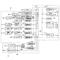
図27は、タグラベル作成装置1′の制御系を表す機能ブロック図であり、前述の図15に対応する図である。この図15と同様の部分には同符号を付し説明を省略する。   FIG. 27 is a functional block diagram showing a control system of the tag label producing apparatus 1 ′ and corresponds to FIG. 15 described above. Parts similar to those in FIG. 15 are denoted by the same reference numerals and description thereof is omitted.

この図27において、装置本体2′は、制御回路110′からの制御信号に基づき、上記送信回路306及び受信回路307と接続される上記アンテナ共用器240を装置本体2′側のループアンテナLC2又はアンテナユニット9側のループアンテナLCに接続するように切り替える切替回路239を有している。すなわち、制御回路110は、装着センサ301からアンテナユニット9の装着状態の検出信号が入力された場合にはタグラベル作成のための書き込みモードに切換えると共に、上記切替回路239を切り替えてアンテナ共用器240とループアンテナLC2とを接続し、装着センサ301からアンテナユニット9の取り外し状態の検出信号が入力された場合には読み取りモードに切換えると共に、上記切替回路239を切り替えてアンテナ共用器240とアンテナユニット9のループアンテナLCとを接続するようになっている。   In FIG. 27, the apparatus main body 2 'connects the antenna duplexer 240 connected to the transmission circuit 306 and the reception circuit 307 to the loop antenna LC2 on the apparatus main body 2' side based on the control signal from the control circuit 110 '. A switching circuit 239 for switching to connect to the loop antenna LC on the antenna unit 9 side is provided. That is, when the detection signal of the mounting state of the antenna unit 9 is input from the mounting sensor 301, the control circuit 110 switches to the writing mode for creating the tag label, and switches the switching circuit 239 to switch the antenna duplexer 240. When the loop antenna LC2 is connected and the detection signal of the detached state of the antenna unit 9 is input from the mounting sensor 301, the mode is switched to the reading mode, and the switching circuit 239 is switched to switch between the antenna duplexer 240 and the antenna unit 9. The loop antenna LC is connected.

図28は、上記制御回路110′によってタグラベル作成時に実行される制御手順を表すフローチャートであり、前述の図21に対応する図である。この図21と同様の手順には同符号を付し説明を省略する。なお、このフローは、書き込みモードとなっている状態で、例えば上記PC118を介しタグラベル作成装置1による所定の無線タグラベル作成操作が行われると開始される。   FIG. 28 is a flowchart showing a control procedure executed at the time of tag label creation by the control circuit 110 ′, and corresponds to FIG. 21 described above. The same steps as those in FIG. 21 are denoted by the same reference numerals and description thereof is omitted. This flow is started when a predetermined RFID label producing operation is performed by the tag label producing apparatus 1 through the PC 118, for example, in the write mode.

この図28において、前述の図21と異なる点は、ステップS103の手順が加わった点である。すなわち、上述したように、装着センサ301からアンテナユニット9の装着状態の検出信号が入力され書き込みモードに切換えると、まずステップS103において、切替回路239に制御信号を出力して切替回路239を切り替え、アンテナ共用器240とループアンテナLC2とを接続させる。その他の手順については、図21と同様であるので説明を省略する。   28 differs from FIG. 21 described above in that the procedure of step S103 is added. That is, as described above, when the detection signal of the mounting state of the antenna unit 9 is input from the mounting sensor 301 and the writing mode is switched, first, in step S103, a control signal is output to the switching circuit 239 to switch the switching circuit 239. The antenna duplexer 240 and the loop antenna LC2 are connected. The other procedures are the same as those in FIG.

図29は、上記制御回路110′によってタグラベル作成装置1′をリーダとして用いる際に実行される制御手順を表すフローチャートであり、前述の図24に対応する図である。この図24と同様の手順には同符号を付し説明を省略する。なお、このフローは、読み取りモードとなっている状態で、操作スイッチ302の操作が行われると開始される。   FIG. 29 is a flowchart showing a control procedure executed when the control circuit 110 ′ uses the tag label producing apparatus 1 ′ as a reader, and corresponds to FIG. 24 described above. The same steps as those in FIG. 24 are denoted by the same reference numerals and description thereof is omitted. This flow starts when the operation switch 302 is operated in the reading mode.

この図29において、前述の図24と異なる点は、ステップS305の手順が加わった点である。このステップS305では、切替回路239に制御信号を出力して切替回路239を切り替え、アンテナ共用器240とアンテナユニット9側のループアンテナLCとを接続させる。その他の手順については、図24と同様であるので説明を省略する。   In FIG. 29, the difference from FIG. 24 described above is that step S305 is added. In step S305, a control signal is output to the switching circuit 239 to switch the switching circuit 239 to connect the antenna duplexer 240 and the loop antenna LC on the antenna unit 9 side. The other procedures are the same as those in FIG.

以上説明した変形例においても、上記実施形態と同様の効果を得ることができる。   Also in the modified examples described above, the same effects as in the above embodiment can be obtained.

(2)モード切換えを手動操作で行う場合
上記実施形態では、装着センサ301からの検出信号に基づき、制御回路110によりアンテナユニット9が装置本体に装着されているかどうかを判定して書き込みモード及び読み取りモードを自動で切換える場合を一例として説明したが、これに限られない。すなわち、例えば操作スイッチ302を用いて操作者が手動で書き込みモード及び読み取りモードを切換えるようにしてもよい。
(2) When switching mode by manual operation In the embodiment described above, based on the detection signal from the mounting sensor 301, the control circuit 110 determines whether or not the antenna unit 9 is mounted on the apparatus main body, thereby writing mode and reading. Although the case where the mode is automatically switched has been described as an example, the present invention is not limited to this. That is, for example, the operator may manually switch between the writing mode and the reading mode using the operation switch 302.

図30は、タグラベル作成装置1″の制御系を表す機能ブロック図であり、前述の図15に対応する図である。この図15と同様の部分には同符号を付し説明を省略する。   FIG. 30 is a functional block diagram showing a control system of the tag label producing apparatus 1 ″ and is a diagram corresponding to the above-described FIG. 15. The same parts as those in FIG.

この図30に示すように、本変形例のタグラベル作成装置1″の装置本体2″は、上記変形例(1)の図27に示す装置本体2′の構成と異なり、装着センサ301を有しない。その他の構成は図15と同様である。   As shown in FIG. 30, the device main body 2 ″ of the tag label producing device 1 ″ of the present modification is different from the device main body 2 ′ shown in FIG. 27 of the modification (1) and does not have the mounting sensor 301. . Other configurations are the same as those in FIG.

図31は、本変形例における制御回路110″によって実行される制御手順を表すフローチャートであり、前述の図20に対応する図である。   FIG. 31 is a flowchart showing a control procedure executed by the control circuit 110 ″ in this modification, and corresponds to FIG. 20 described above.

この図31において、ステップS1Aでは、操作スイッチ302からの操作信号が入力されたかどうかを判定する。入力があった場合には、ステップS1Aの判定が満たされ、ステップS300の読み取りモードに移る。一方、操作信号の入力がない場合には、ステップS1Aの判定が満たされず、ステップS100の書き込みモードに移る。このように、本変形例では、アンテナユニット9の装着状態に応じて自動でモードの切り替えを行うのではなく、操作スイッチ302の操作入力によって読み取りモードへの切り替えを行う。なお、本変形例では、ステップS300で読み取りモードとなった後、そのまま図24に示すフローが開始されるようになっている。なお、動作モードの設定はアンテナユニット9に設けられた操作スイッチ302による入力に限られるものではなく、装置本体2に設けた適宜の入力手段により動作モードを設定するようにしてもよい。   In FIG. 31, in step S1A, it is determined whether or not an operation signal from the operation switch 302 has been input. If there is an input, the determination in step S1A is satisfied, and the process proceeds to the reading mode in step S300. On the other hand, if no operation signal is input, the determination in step S1A is not satisfied and the writing mode in step S100 is entered. As described above, in this modification, the mode is not automatically switched according to the mounting state of the antenna unit 9 but is switched to the reading mode by the operation input of the operation switch 302. In the present modification, after entering the reading mode in step S300, the flow shown in FIG. 24 is started as it is. Note that the setting of the operation mode is not limited to input by the operation switch 302 provided in the antenna unit 9, and the operation mode may be set by an appropriate input means provided in the apparatus main body 2.

以上説明した変形例においても、上記実施形態と同様の効果を得ることができる。また、装着センサが不要なため、装置構成の簡素化及びコスト低減を図ることができる。   Also in the modified examples described above, the same effects as in the above embodiment can be obtained. In addition, since a mounting sensor is unnecessary, the device configuration can be simplified and the cost can be reduced.

(3)その他
以上においては、装置側のアンテナLCや無線タグ回路素子To側のアンテナ152としてループアンテナを用い、磁気誘導(電磁誘導、磁気結合、その他電磁界を介して行われる非接触方式を含む)により情報送受信を行ったが、これに限られず、例えば上記アンテナとしてダイポールアンテナやパッチアンテナ等を送受信手段として用い、反射を利用した電波通信により情報送受信を行うようにしてもよい。
(3) Others In the above, a loop antenna is used as the antenna LC on the device side and the antenna 152 on the RFID tag circuit element To side, and magnetic induction (electromagnetic induction, magnetic coupling, other non-contact methods performed via electromagnetic fields are used. However, the present invention is not limited to this. For example, a dipole antenna, a patch antenna, or the like may be used as the transmission / reception means, and information transmission / reception may be performed by radio wave communication using reflection.

また、以上は、装置本体2の上側に開閉蓋3を有し、当該上側にカートリッジ7を横置き状態で装着するタグラベル作成装置(いわゆるカートリッジ横置きタイプ)を例にとって説明したが、これに限られず、装置本体の側方側に開閉蓋を有し、当該側方側にカートリッジ7を縦置き状態で装着するタグラベル作成装置(いわゆるカートリッジ縦置きタイプ)に本発明を適用してもよい。   In the above description, the tag label producing apparatus (so-called cartridge horizontal type) in which the opening / closing lid 3 is provided on the upper side of the apparatus main body 2 and the cartridge 7 is mounted in the horizontal position on the upper side has been described as an example. Alternatively, the present invention may be applied to a tag label producing apparatus (so-called cartridge vertical installation type) having an open / close lid on the side of the apparatus main body and mounting the cartridge 7 in the vertical position on the side.

また、以上は、アンテナユニット9と装置本体2とをケーブル223を用いてケーブル接続するようにしたが、これに限られず、アンテナユニット9と装置本体2との間で、無線通信により信号の送受を行うようにしてもよい。   In the above, the antenna unit 9 and the apparatus main body 2 are cable-connected using the cable 223. However, the present invention is not limited to this, and signals are transmitted and received between the antenna unit 9 and the apparatus main body 2 by wireless communication. May be performed.

また、以上は、無線タグ回路素子Toに対し無線タグ情報を送信しIC回路部151に書き込みを行って無線タグラベルTを作成する場合を説明したが、これに限られない。すなわち、既に触れたように、予め所定の無線タグ情報が書き換え不可に記憶保持されている読み取り専用の無線タグ回路素子Toから無線タグ情報を読み取りながら、これに対応する印字を行って無線タグラベルTを作成する場合にも本発明は適用でき、この場合も上記同様の効果を得ることができる。   In the above description, the RFID tag information T is transmitted to the RFID circuit element To and written to the IC circuit unit 151 to create the RFID tag T. However, the present invention is not limited to this. That is, as already mentioned, while reading the RFID tag information from the read-only RFID circuit element To in which predetermined RFID tag information is stored and retained in a non-rewritable manner, printing corresponding to the RFID tag information T is performed. The present invention can also be applied to the case of creating the image, and also in this case, the same effect as described above can be obtained.

また、以上においては、無線タグ回路素子Toを備えた基材テープ101とは別のカバーフィルム103に印字を行ってこれらを貼り合わせる方式であったが、これに限られず、例えばタグテープに備えられた被印字テープ層の印字領域に印字を行う方式(貼りあわせを行わないタイプ)に本発明を適用してもよい。この場合、ハーフカットユニット35において受け台38とハーフカッタ34の構成は本実施形態とは異なったものとなる。すなわち図9のハーフカッタ34側に受け台が配置され、受け台38側にハーフカッタが配置される。   Moreover, in the above, it was the system which prints on the cover film 103 different from the base-material tape 101 provided with the RFID circuit element To, and bonds these together, but it is not restricted to this, For example, it prepares for a tag tape. The present invention may be applied to a method (a type in which bonding is not performed) in which printing is performed on a printing region of the printed tape layer. In this case, the configurations of the cradle 38 and the half cutter 34 in the half cut unit 35 are different from those of the present embodiment. That is, the cradle is disposed on the half cutter 34 side of FIG. 9 and the half cutter is disposed on the cradle 38 side.

また、以上において、印字及び無線タグ回路素子Toへのアクセス(読み取り又は書き込み)の終了した印字済みタグラベル用テープ109を切断機構15で切断してタグラベルTを作成した場合を例にとって説明したが、これに限られない。すなわち、ラベルに対応した所定の大きさに予め分離されたラベル台紙(いわゆるダイカットラベル)がロールから繰り出されるテープ上に連続配置されているような場合には、切断機構15で切断しなくても、テープがラベル排出口11から排出されてきた後にラベル台紙(アクセス済みの無線タグ回路素子Toが備えられかつ対応する印字がなされたもの)のみをテープから剥がしてタグラベルTを作成しても良く、本発明はこのようなものに対しても適用できる。   In the above description, the case where the tag label T is generated by cutting the printed tag label tape 109 after printing and access (reading or writing) to the RFID circuit element To by the cutting mechanism 15 has been described. It is not limited to this. That is, when the label mount (so-called die-cut label) separated in advance to a predetermined size corresponding to the label is continuously arranged on the tape fed out from the roll, the cutting mechanism 15 does not need to cut the label mount. After the tape has been discharged from the label discharge port 11, only the label mount (the one with the already accessed RFID circuit element To and the corresponding printing performed) may be peeled off from the tape to produce the tag label T. The present invention is also applicable to such a case.

さらに、以上は、基材テープ101がリール部材102aの周りに巻回されて第1ロール102を構成し、カートリッジ7内にそのロールが配置されて基材テープ101が繰り出される場合を例にとって説明したが、これに限られない。例えば、無線タグ回路素子Toが少なくとも一つ配置された長尺平紙状あるいは短冊状のテープやシート(ロールに巻回されたテープを繰り出した後に適宜の長さに切断して形成したものを含む)を、所定の収納部にスタックして(例えばトレイ状のものに平積み積層して)カートリッジ化し、このカートリッジをタグラベル作成装置側のカートリッジホルダに装着して、上記収納部から移送、搬送して印字及び書き込みを行いタグラベルを作成するようにしてもよい。   Further, the above description is given taking as an example the case where the base tape 101 is wound around the reel member 102a to form the first roll 102, the roll is arranged in the cartridge 7 and the base tape 101 is fed out. However, it is not limited to this. For example, a long flat paper-like or strip-like tape or sheet in which at least one RFID circuit element To is arranged (the one formed by cutting a tape wound around a roll and cutting it to an appropriate length) Are stacked in a predetermined storage unit (for example, stacked in a tray shape) to form a cartridge, and the cartridge is attached to the cartridge holder on the tag label producing apparatus side, and is transported and transported from the storage unit. The tag label may be created by printing and writing.

さらには上記ロールを直接タグラベル作成装置側に着脱可能に装着する構成や、長尺平紙状あるいは短冊状のテープやシートをタグラベル作成装置外より1枚ずつ所定のフィーダ機構によって移送しタグラベル作成装置内へ供給する構成も考えられ、さらにはカートリッジ7のようなタグラベル作成装置本体側に着脱可能なものにも限られず、装置本体側に着脱不能のいわゆる据え付け型あるいは一体型として第1ロール102を設けることも考えられる。この場合も同様の効果を得る。   Further, a structure in which the above roll is directly detachably attached to the tag label producing apparatus side, or a long flat paper-like or strip-like tape or sheet is transferred one by one from the outside of the tag label producing apparatus by a predetermined feeder mechanism. The first roll 102 is not limited to the tag label producing apparatus main body side such as the cartridge 7 and can be attached to the apparatus main body side. It is also possible to provide it. In this case, the same effect is obtained.

なお、以上で用いた「Scroll ID」信号、「Erase」信号、「Verify」信号、「Program」信号等は、EPC globalが策定した仕様に準拠しているものとする。EPC globalは、流通コードの国際機関である国際EAN協会と、米国の流通コード機関であるUniformed Code Council(UCC)が共同で設立した非営利法人である。なお、他の規格に準拠した信号でも、同様の機能を果たすものであればよい。   It is assumed that the “Scroll ID” signal, “Erase” signal, “Verify” signal, “Program” signal, etc. used above conform to the specifications established by EPC global. EPC global is a non-profit corporation established jointly by the International EAN Association, which is an international organization of distribution codes, and the United Code Code Council (UCC), which is an American distribution code organization. Note that signals conforming to other standards may be used as long as they perform the same function.

また、以上既に述べた以外にも、上記実施形態や各変形例による手法を適宜組み合わせて利用しても良い。   In addition to those already described above, the methods according to the above-described embodiments and modifications may be used in appropriate combination.

その他、一々例示はしないが、本発明は、その趣旨を逸脱しない範囲内において、種々の変更が加えられて実施されるものである   In addition, although not illustrated one by one, the present invention is implemented with various modifications within a range not departing from the gist thereof.

本発明の一実施形態であるタグラベル作成装置を備えた無線タグ生成システムを表すシステム構成図である。1 is a system configuration diagram illustrating a wireless tag generation system including a tag label producing apparatus according to an embodiment of the present invention. タグラベル作成装置の全体構造を表す斜視図である。It is a perspective view showing the whole tag label production apparatus structure. タグラベル作成装置の全体構造を表す斜視図である。It is a perspective view showing the whole tag label production apparatus structure. タグラベル作成装置の内部の内部ユニットの構造を表す平面図である。It is a top view showing the structure of the internal unit inside a tag label production apparatus. カートリッジの詳細構造を模式的に表す拡大平面図である。FIG. 4 is an enlarged plan view schematically showing a detailed structure of a cartridge. 第1ロールより繰り出された基材テープに備えられる無線タグ回路素子の概念的構成を表す図5中矢印D方向から見た概念図である。It is the conceptual diagram seen from the arrow D direction in FIG. 5 showing the notional structure of the RFID circuit element with which the base tape extended | stretched from the 1st roll is equipped. ラベル排出機構の要部詳細構造を表す部分抽出斜視図、及びマークセンサの概念的構成を表す図である。It is the partial extraction perspective view showing the principal part detailed structure of a label discharge mechanism, and the figure showing the conceptual structure of a mark sensor. 図4に示した構造からラベル排出機構及びアンテナユニットを取り外した状態における内部ユニットの外観を表す斜視図である。It is a perspective view showing the external appearance of the internal unit in the state which removed the label discharge | emission mechanism and the antenna unit from the structure shown in FIG. 内部ユニットよりハーフカッタを除去した、切断機構の外観を表す斜視図である。It is a perspective view showing the external appearance of the cutting mechanism which removed the half cutter from the internal unit. 内部ユニットよりハーフカッタを除去した、切断機構の外観を表す斜視図である。It is a perspective view showing the external appearance of the cutting mechanism which removed the half cutter from the internal unit. 可動刃及び固定刃の詳細構造をハーフカットユニットともに表す斜視図である。It is a perspective view showing the detailed structure of a movable blade and a fixed blade with a half cut unit. 可動刃及び固定刃の詳細構造をハーフカットユニットともに表す部分拡大断面図である。It is a partial expanded sectional view showing the detailed structure of a movable blade and a fixed blade with a half cut unit. 可動刃の外観を示す正面図である。It is a front view which shows the external appearance of a movable blade. 図13中A−A断面による横断面図である。It is a cross-sectional view by the AA cross section in FIG. 本発明の一実施形態であるタグラベル作成装置の制御系を表す機能ブロック図である。It is a functional block diagram showing the control system of the tag label production apparatus which is one Embodiment of this invention. 無線タグ回路素子の機能的構成を表す機能ブロック図である。It is a functional block diagram showing the functional structure of a wireless tag circuit element. タグラベル作成装置により無線タグ回路素子の情報書き込み(又は読み取り)及び印字済タグラベル用テープの切断が完了し形成された無線タグラベルの外観の一例を表す上面図及び下面図である。FIG. 4 is a top view and a bottom view showing an example of the appearance of a RFID label formed by completing writing (or reading) information of a RFID circuit element and cutting of a tag label tape with print by a tag label producing device. 図17中XVIIIA−XVIIIA′断面による横断面図を反時計方向に90°回転させた図及び図17中XVIIIB−XVIIIB′断面による横断面図を反時計方向に90°回転させた図、及び識別マークとしてレーザ加工等により基材テープを略貫通する孔を孔設する場合の無線タグラベルの下面図である。FIG. 17 is a cross-sectional view of the XVIIIA-XVIIIA ′ cross section rotated 90 ° counterclockwise, and FIG. 17 is a cross-sectional view of the XVIIIB-XVIIIB ′ cross section rotated 90 ° counterclockwise. It is a bottom view of the RFID label in the case where a hole substantially penetrating through the base tape is provided as a mark by laser processing or the like. タグラベル作成装置による無線タグ回路素子のIC回路部の無線タグ情報へのアクセス(読み取り又は書き込み)に際して、PC(端末又は汎用コンピュータ)に表示される画面の一例を表す図である。It is a figure showing an example of the screen displayed on PC (terminal or general-purpose computer) at the time of access (reading or writing) to the RFID tag information of the IC circuit part of the RFID circuit element by the tag label producing device. 制御回路によって実行される制御手順を表すフローチャートである。It is a flowchart showing the control procedure performed by the control circuit. タグラベル作成時に制御回路によって実行される制御手順を表すフローチャートである。It is a flowchart showing the control procedure performed by a control circuit at the time of tag label creation. ステップS200の詳細手順を表すフローチャートである。It is a flowchart showing the detailed procedure of step S200. ステップS400の詳細手順を表すフローチャートである。It is a flowchart showing the detailed procedure of step S400. タグラベル作成装置をリーダとして使用する際に制御回路によって実行される制御手順を表すフローチャートである。It is a flowchart showing the control procedure performed by a control circuit when using a tag label production apparatus as a reader. シールド板をアンテナユニットに設ける場合の変形例におけるタグラベル作成装置の全体構造を表す斜視図である。It is a perspective view showing the whole structure of the tag label production apparatus in the modification in the case of providing a shield board in an antenna unit. シールド板をアンテナユニットに設ける場合の変形例におけるタグラベル作成装置の内部構造を表す平面図である。It is a top view showing the internal structure of the tag label production apparatus in the modification in the case of providing a shield board in an antenna unit. シールド板をアンテナユニットに設ける場合の変形例におけるタグラベル作成装置の制御系を表す機能ブロック図である。It is a functional block diagram showing the control system of the tag label production apparatus in the modification in the case of providing a shield board in an antenna unit. シールド板をアンテナユニットに設ける場合の変形例において、制御回路によってタグラベル作成時に実行される制御手順を表すフローチャートである。It is a flowchart showing the control procedure performed at the time of tag label preparation by a control circuit in the modification in the case of providing a shield board in an antenna unit. シールド板をアンテナユニットに設ける場合の変形例において、制御回路によってタグラベル作成装置をリーダとして用いる際に実行される制御手順を表すフローチャートである。It is a flowchart showing the control procedure performed when using a tag label production apparatus as a reader | leader by a control circuit in the modification in the case of providing a shield board in an antenna unit. モード切換えを手動操作で行う場合の変形例におけるタグラベル作成装置の制御系を表す機能ブロック図である。It is a functional block diagram showing the control system of the tag label production apparatus in the modification in the case of performing mode switching by manual operation. モード切換えを手動操作で行う場合の変形例における制御回路によって実行される制御手順を表すフローチャートである。It is a flowchart showing the control procedure performed by the control circuit in the modification in the case of performing mode switching by manual operation.

符号の説明Explanation of symbols

1 タグラベル作成装置
1′ タグラベル作成装置
1″ タグラベル作成装置
2 装置本体(タグラベル作成装置本体)
9 アンテナユニット
51 駆動ローラ(搬送手段)
109 印字済みタグラベル用テープ(タグ媒体)
110 制御回路(情報生成手段、出力制御手段)
110′制御回路(情報生成手段、出力制御手段)
110″制御回路(情報生成手段、出力制御手段)
151 IC回路部
152 ループアンテナ(タグ側アンテナ)
200 筐体
201 係合部
223 ケーブル(導線部材)
234 把持部
235 磁性部材(規制手段)
236 シールド板(規制手段)
301 装着センサ(検出手段)
302 操作スイッチ(操作手段)
LC ループアンテナ(ユニット側アンテナ)
To 無線タグ回路素子
DESCRIPTION OF SYMBOLS 1 Tag label production apparatus 1 'Tag label production apparatus 1 "Tag label production apparatus 2 Apparatus main body (tag label production apparatus main body)
9 Antenna unit 51 Driving roller (conveying means)
109 Printed tag label tape (tag medium)
110 Control circuit (information generating means, output control means)
110 'control circuit (information generating means, output control means)
110 "control circuit (information generating means, output control means)
151 IC circuit section 152 Loop antenna (tag side antenna)
200 Housing 201 Engaging portion 223 Cable (conductor member)
234 Grasping part 235 Magnetic member (regulating means)
236 Shield plate (regulation means)
301 Wear sensor (detection means)
302 Operation switch (operation means)
LC loop antenna (unit side antenna)
To RFID tag circuit element

Claims (12)

タグラベル作成装置本体と、
このタグラベル作成装置本体に着脱可能なアンテナユニットとを有するタグラベル作成装置であって、
前記アンテナユニットは、
情報を記憶するIC回路部と情報の送受信を行うタグ側アンテナとを備えた無線タグ回路素子との間で無線通信により情報の送受信を行うユニット側アンテナを有し、
前記タグラベル作成装置本体は、
前記アンテナユニットを係合するための係合部を備えた筐体と、
この筐体内に設けられ、前記無線タグ回路素子を配置したタグ媒体を搬送する搬送手段と、
この搬送手段によって搬送される前記タグ媒体の前記無線タグ回路素子にアクセスするためのアクセス情報を生成する情報生成手段と
を有することを特徴とするタグラベル作成装置。
A tag label producing device,
A tag label producing device having an antenna unit detachable from the tag label producing device main body,
The antenna unit is
A unit-side antenna that transmits and receives information by wireless communication between an IC circuit unit that stores information and a tag-side antenna that transmits and receives information;
The tag label producing apparatus main body is
A housing having an engaging portion for engaging the antenna unit;
A conveying means that is provided in the casing and conveys a tag medium in which the RFID circuit elements are arranged;
A tag label producing apparatus comprising: information generating means for generating access information for accessing the RFID circuit elements of the tag medium carried by the carrying means.
請求項1記載のタグラベル作成装置において、
前記アンテナユニットの前記ユニット側アンテナは、前記係合部へ装着したときと、取り外したときとで、その通信可能範囲が異なるように構成されていることを特徴とするタグラベル作成装置。
In the tag label producing apparatus according to claim 1,
The tag label producing apparatus, wherein the unit side antenna of the antenna unit is configured so that a communicable range is different between when the antenna is attached to the engaging portion and when the antenna is removed.
請求項2記載のタグラベル作成装置において、
前記タグラベル作成装置本体は、前記アンテナユニットを前記係合部に装着したときと取り外したときとで前記ユニット側アンテナによる送信出力を切り替えて増減させる出力制御手段を備えることを特徴とするタグラベル作成装置。
In the tag label producing apparatus according to claim 2,
The tag label producing apparatus main body comprises an output control means for switching the transmission output by the unit side antenna to be increased or decreased depending on whether the antenna unit is attached to or removed from the engaging portion. .
請求項2記載のタグラベル作成装置において、
前記タグラベル作成装置本体は、前記アンテナユニットを前記係合部に装着したときに、前記ユニット側アンテナの通信可能範囲を規制する規制手段を有することを特徴とするタグラベル作成装置。
In the tag label producing apparatus according to claim 2,
The tag label producing apparatus has a restricting means for restricting a communicable range of the unit side antenna when the antenna unit is attached to the engaging portion.
請求項4記載のタグラベル作成装置において、
前記規制手段は、
前記アンテナユニットを前記係合部に装着したときに、前記ユニット側アンテナによる、前記タグ媒体に備えられた通信対象となる前記無線タグ回路素子以外の無線タグ回路素子への電磁波の放射を抑制するように、配置されていることを特徴とするタグラベル作成装置。
In the tag label production apparatus according to claim 4,
The regulating means is
When the antenna unit is attached to the engaging portion, the unit-side antenna suppresses the emission of electromagnetic waves to wireless tag circuit elements other than the wireless tag circuit element to be communicated provided in the tag medium. A tag label producing apparatus characterized by being arranged as described above.
請求項4記載のタグラベル作成装置において、
前記規制手段は、
前記アンテナユニットを前記係合部に装着したときに、前記ユニット側アンテナによる前記タグラベル作成装置本体の外方への電磁波の放射を抑制するように、配置されていることを特徴とするタグラベル作成装置。
In the tag label production apparatus according to claim 4,
The regulating means is
When the antenna unit is mounted on the engaging portion, the tag label producing device is arranged so as to suppress radiation of electromagnetic waves to the outside of the tag label producing device main body by the unit side antenna. .
請求項1乃至6のいずれか1項記載のタグラベル作成装置において、
前記アンテナユニットを前記係合部に装着したときは、主として前記搬送手段で搬送される前記タグ媒体に備えられた前記無線タグ回路素子の前記IC回路部へ所望の無線タグ情報を書き込むための書き込みモードとなり、
前記アンテナユニットを前記係合部から取り外したときは、主としてタグラベル作成装置外に存在する前記無線タグ回路素子の前記IC回路部より当該無線タグ回路素子の識別情報を取得するための読み取りモードとなるように、
前記情報生成手段を制御するモード制御手段を有することを特徴とするタグラベル作成装置。
In the tag label production apparatus according to any one of claims 1 to 6,
When the antenna unit is attached to the engaging portion, writing for writing desired RFID tag information to the IC circuit portion of the RFID tag circuit element provided in the tag medium mainly carried by the carrier means Mode,
When the antenna unit is removed from the engaging portion, the reading mode for acquiring the identification information of the RFID circuit element is mainly obtained from the IC circuit portion of the RFID circuit element existing outside the tag label producing apparatus. like,
A tag label producing apparatus comprising mode control means for controlling the information generating means.
請求項7記載のタグラベル作成装置において、
前記アンテナユニットは、
前記読み取りモードにおいて前記識別情報の取得動作を開始するための操作手段を有することを特徴とするタグラベル作成装置。
In the tag label production apparatus according to claim 7,
The antenna unit is
An apparatus for producing a tag label, comprising operation means for starting an operation for acquiring the identification information in the reading mode.
請求項8記載のタグラベル作成装置において、
前記操作手段は、前記アンテナユニットと前記タグラベル作成装置本体とを接続する導線部材を介し、前記情報生成手段と接続されている
ことを特徴とするタグラベル作成装置。
In the tag label production apparatus according to claim 8,
The tag label producing apparatus, wherein the operating means is connected to the information generating means via a conductor member connecting the antenna unit and the tag label producing apparatus main body.
請求項8又は9のいずれか1項記載のタグラベル作成装置において、
前記アンテナユニットは、前記操作手段の操作を行う際に操作者が把持するための把持部を備えていることを特徴とするタグラベル作成装置。
In the tag label production apparatus according to any one of claims 8 and 9,
The tag label producing apparatus according to claim 1, wherein the antenna unit includes a grip portion for an operator to grip when operating the operation means.
請求項1乃至10のいずれか1項記載のタグラベル作成装置において、
前記アンテナユニットは、
その一方側端部に、前記筐体の前記係合部に係合される被係合部を備え、
その他方側端部は、前記筐体の前記係合部に係合不能となるような、前記被係合部と異なる形状を備えている
ことを特徴とするタグラベル作成装置。
In the tag label production apparatus according to any one of claims 1 to 10,
The antenna unit is
At one end thereof, an engaged portion that is engaged with the engaging portion of the housing is provided,
The tag label producing apparatus according to claim 1, wherein the other side end portion has a shape different from that of the engaged portion so as not to be engaged with the engaging portion of the housing.
請求項1乃至11のいずれか1項記載のタグラベル作成装置において、
前記アンテナユニットが前記係合部へ装着されているかどうかを検出する検出手段を有することを特徴とするタグラベル作成装置。
The tag label producing apparatus according to any one of claims 1 to 11,
A tag label producing apparatus comprising detecting means for detecting whether or not the antenna unit is attached to the engaging portion.
JP2006094824A 2006-02-20 2006-03-30 Tag label making device Expired - Fee Related JP4636384B2 (en)

Priority Applications (2)

Application Number Priority Date Filing Date Title
JP2006094824A JP4636384B2 (en) 2006-03-30 2006-03-30 Tag label making device
PCT/JP2007/052983 WO2007097288A1 (en) 2006-02-20 2007-02-19 Label medium treating device and engaging/disengaging unit

Applications Claiming Priority (1)

Application Number Priority Date Filing Date Title
JP2006094824A JP4636384B2 (en) 2006-03-30 2006-03-30 Tag label making device

Publications (2)

Publication Number Publication Date
JP2007272371A JP2007272371A (en) 2007-10-18
JP4636384B2 true JP4636384B2 (en) 2011-02-23

Family

ID=38675137

Family Applications (1)

Application Number Title Priority Date Filing Date
JP2006094824A Expired - Fee Related JP4636384B2 (en) 2006-02-20 2006-03-30 Tag label making device

Country Status (1)

Country Link
JP (1) JP4636384B2 (en)

Families Citing this family (2)

* Cited by examiner, † Cited by third party
Publication number Priority date Publication date Assignee Title
KR101265208B1 (en) * 2011-06-01 2013-05-27 주식회사 모텍스 Apparatus for encoding of RFID label
KR101265209B1 (en) * 2011-06-02 2013-05-27 주식회사 모텍스 Apparatus for encoding of RFID label

Citations (2)

* Cited by examiner, † Cited by third party
Publication number Priority date Publication date Assignee Title
JPH0586945U (en) * 1992-05-06 1993-11-22 セイコー電子工業株式会社 Paper edge detection structure
JP2000052612A (en) * 1998-08-06 2000-02-22 Toshiba Tec Corp Label printer

Patent Citations (2)

* Cited by examiner, † Cited by third party
Publication number Priority date Publication date Assignee Title
JPH0586945U (en) * 1992-05-06 1993-11-22 セイコー電子工業株式会社 Paper edge detection structure
JP2000052612A (en) * 1998-08-06 2000-02-22 Toshiba Tec Corp Label printer

Also Published As

Publication number Publication date
JP2007272371A (en) 2007-10-18

Similar Documents

Publication Publication Date Title
JP2007326307A (en) Tag label making apparatus
JP4771282B2 (en) Tag label making device
JP4692762B2 (en) Wireless tag information communication device
JP4780391B2 (en) Label making device
JP2007328540A (en) Tag label formation device
JP4406846B2 (en) Tag label making device
JP2008021282A (en) Label body and label body producing apparatus
JP2007256857A (en) Wireless tag label, tag tape roll, wireless tag circuit element cartridge, tag label preparing apparatus
JP2007191253A (en) Label preparation device and cartridge for preparing label
JP4730172B2 (en) Label making device
JP4915323B2 (en) Wireless tag information communication device
JP4636384B2 (en) Tag label making device
JP2008171193A (en) Tag label preparation device
JP4640710B2 (en) Tag label production system and antenna module unit
JP2008134831A (en) Tag label creation system and antenna unit
JP2007272372A (en) System for making tab label and antenna module unit
JP5041287B2 (en) Wireless tag information communication device
JP4600774B2 (en) Label making device
JP2008171192A (en) Tag label preparation device and radio circuit element cartridge
JP4911342B2 (en) Tag label making device
JP4858768B2 (en) RFID tag circuit element cartridge and tag label producing apparatus
JP2007334535A (en) Wireless tag information communication device and antenna module unit
WO2010103864A1 (en) Printed label producing device
JP4600740B2 (en) Radio tag circuit element cartridge and radio tag information communication apparatus
JP2009096152A (en) Label preparing apparatus

Legal Events

Date Code Title Description
A621 Written request for application examination

Free format text: JAPANESE INTERMEDIATE CODE: A621

Effective date: 20080328

TRDD Decision of grant or rejection written
A01 Written decision to grant a patent or to grant a registration (utility model)

Free format text: JAPANESE INTERMEDIATE CODE: A01

Effective date: 20101029

A01 Written decision to grant a patent or to grant a registration (utility model)

Free format text: JAPANESE INTERMEDIATE CODE: A01

A61 First payment of annual fees (during grant procedure)

Free format text: JAPANESE INTERMEDIATE CODE: A61

Effective date: 20101111

FPAY Renewal fee payment (event date is renewal date of database)

Free format text: PAYMENT UNTIL: 20131203

Year of fee payment: 3

R150 Certificate of patent or registration of utility model

Free format text: JAPANESE INTERMEDIATE CODE: R150

LAPS Cancellation because of no payment of annual fees