JP4635863B2 - Surface emitting device - Google Patents
Surface emitting device Download PDFInfo
- Publication number
- JP4635863B2 JP4635863B2 JP2005371974A JP2005371974A JP4635863B2 JP 4635863 B2 JP4635863 B2 JP 4635863B2 JP 2005371974 A JP2005371974 A JP 2005371974A JP 2005371974 A JP2005371974 A JP 2005371974A JP 4635863 B2 JP4635863 B2 JP 4635863B2
- Authority
- JP
- Japan
- Prior art keywords
- light
- emitting device
- emitting diode
- light emitting
- reflector
- Prior art date
- Legal status (The legal status is an assumption and is not a legal conclusion. Google has not performed a legal analysis and makes no representation as to the accuracy of the status listed.)
- Expired - Fee Related
Links
Images

Classifications
-
- G—PHYSICS
- G02—OPTICS
- G02F—OPTICAL DEVICES OR ARRANGEMENTS FOR THE CONTROL OF LIGHT BY MODIFICATION OF THE OPTICAL PROPERTIES OF THE MEDIA OF THE ELEMENTS INVOLVED THEREIN; NON-LINEAR OPTICS; FREQUENCY-CHANGING OF LIGHT; OPTICAL LOGIC ELEMENTS; OPTICAL ANALOGUE/DIGITAL CONVERTERS
- G02F1/00—Devices or arrangements for the control of the intensity, colour, phase, polarisation or direction of light arriving from an independent light source, e.g. switching, gating or modulating; Non-linear optics
- G02F1/01—Devices or arrangements for the control of the intensity, colour, phase, polarisation or direction of light arriving from an independent light source, e.g. switching, gating or modulating; Non-linear optics for the control of the intensity, phase, polarisation or colour
- G02F1/13—Devices or arrangements for the control of the intensity, colour, phase, polarisation or direction of light arriving from an independent light source, e.g. switching, gating or modulating; Non-linear optics for the control of the intensity, phase, polarisation or colour based on liquid crystals, e.g. single liquid crystal display cells
- G02F1/133—Constructional arrangements; Operation of liquid crystal cells; Circuit arrangements
- G02F1/1333—Constructional arrangements; Manufacturing methods
- G02F1/1335—Structural association of cells with optical devices, e.g. polarisers or reflectors
- G02F1/1336—Illuminating devices
- G02F1/133602—Direct backlight
- G02F1/133605—Direct backlight including specially adapted reflectors
-
- G—PHYSICS
- G02—OPTICS
- G02F—OPTICAL DEVICES OR ARRANGEMENTS FOR THE CONTROL OF LIGHT BY MODIFICATION OF THE OPTICAL PROPERTIES OF THE MEDIA OF THE ELEMENTS INVOLVED THEREIN; NON-LINEAR OPTICS; FREQUENCY-CHANGING OF LIGHT; OPTICAL LOGIC ELEMENTS; OPTICAL ANALOGUE/DIGITAL CONVERTERS
- G02F1/00—Devices or arrangements for the control of the intensity, colour, phase, polarisation or direction of light arriving from an independent light source, e.g. switching, gating or modulating; Non-linear optics
- G02F1/01—Devices or arrangements for the control of the intensity, colour, phase, polarisation or direction of light arriving from an independent light source, e.g. switching, gating or modulating; Non-linear optics for the control of the intensity, phase, polarisation or colour
- G02F1/13—Devices or arrangements for the control of the intensity, colour, phase, polarisation or direction of light arriving from an independent light source, e.g. switching, gating or modulating; Non-linear optics for the control of the intensity, phase, polarisation or colour based on liquid crystals, e.g. single liquid crystal display cells
- G02F1/133—Constructional arrangements; Operation of liquid crystal cells; Circuit arrangements
- G02F1/1333—Constructional arrangements; Manufacturing methods
- G02F1/1335—Structural association of cells with optical devices, e.g. polarisers or reflectors
- G02F1/1336—Illuminating devices
- G02F1/133602—Direct backlight
- G02F1/133603—Direct backlight with LEDs
-
- G—PHYSICS
- G02—OPTICS
- G02F—OPTICAL DEVICES OR ARRANGEMENTS FOR THE CONTROL OF LIGHT BY MODIFICATION OF THE OPTICAL PROPERTIES OF THE MEDIA OF THE ELEMENTS INVOLVED THEREIN; NON-LINEAR OPTICS; FREQUENCY-CHANGING OF LIGHT; OPTICAL LOGIC ELEMENTS; OPTICAL ANALOGUE/DIGITAL CONVERTERS
- G02F1/00—Devices or arrangements for the control of the intensity, colour, phase, polarisation or direction of light arriving from an independent light source, e.g. switching, gating or modulating; Non-linear optics
- G02F1/01—Devices or arrangements for the control of the intensity, colour, phase, polarisation or direction of light arriving from an independent light source, e.g. switching, gating or modulating; Non-linear optics for the control of the intensity, phase, polarisation or colour
- G02F1/13—Devices or arrangements for the control of the intensity, colour, phase, polarisation or direction of light arriving from an independent light source, e.g. switching, gating or modulating; Non-linear optics for the control of the intensity, phase, polarisation or colour based on liquid crystals, e.g. single liquid crystal display cells
- G02F1/133—Constructional arrangements; Operation of liquid crystal cells; Circuit arrangements
- G02F1/1333—Constructional arrangements; Manufacturing methods
- G02F1/1335—Structural association of cells with optical devices, e.g. polarisers or reflectors
- G02F1/1336—Illuminating devices
- G02F1/133602—Direct backlight
- G02F1/133611—Direct backlight including means for improving the brightness uniformity
Landscapes
- Physics & Mathematics (AREA)
- Nonlinear Science (AREA)
- Mathematical Physics (AREA)
- Chemical & Material Sciences (AREA)
- Crystallography & Structural Chemistry (AREA)
- General Physics & Mathematics (AREA)
- Optics & Photonics (AREA)
- Liquid Crystal (AREA)
- Planar Illumination Modules (AREA)
- Led Device Packages (AREA)
Description
本発明は、複数の光源を用いた面発光装置、特に、比較的大面積の発光面を有する面発光装置に関する。 The present invention relates to a surface light-emitting device using a plurality of light sources, and more particularly to a surface light-emitting device having a relatively large light-emitting surface.
現在、液晶表示装置が携帯電子機器や各種画像表示機器に広く利用されている。液晶表示装置は、液晶セル、プリズムシート、拡散シート及びバックライト等を主要な構成要素として構成され、このバックライト光源には、LEDを用いたバックライト光源や冷陰極管を用いたバックライト光源などがある。これらのバックライト光源にはそれぞれ特色があり、比較的大型の液晶表示装置には冷陰極管を用いたバックライト光源が多く用いられ、例えば、携帯電話に用いられる小型の液晶表示装置にはLEDを用いたバックライト光源が多く使用されるなど、用途に応じて使い分けられている。 Currently, liquid crystal display devices are widely used in portable electronic devices and various image display devices. The liquid crystal display device includes a liquid crystal cell, a prism sheet, a diffusion sheet, a backlight, and the like as main components. The backlight light source includes a backlight light source using an LED and a backlight light source using a cold cathode tube. and so on. Each of these backlight light sources has its own characteristics. For relatively large liquid crystal display devices, many backlight light sources using cold cathode tubes are used. For example, small liquid crystal display devices used for mobile phones have LED. For example, a backlight light source using a light source is often used.
また、これらのバックライト光源は、いずれも導光板を用いて、線光源である冷陰極型蛍光ランプ又は点光源である発光ダイオードからの光を発光面全体に拡げて面発光させるものであり、発光面全体が均一な輝度になるように種々の工夫がなされている。
しかしながら、このバックライト光源にとって必須の構成要素である導光板が、比較的大型の液晶表示装置用のバックライト光源の軽量化や薄型化の妨げとなっていた。
このような状況の下、光が導波する部分を中空にした、導光板レス(導光板を有しない)のバックライト光源も開発され始めている(特許文献1の図13、図14)。
However, the light guide plate, which is an essential component for the backlight light source, has hindered the weight reduction and thinning of the backlight light source for relatively large liquid crystal display devices.
Under such circumstances, a light source plate-less (without a light guide plate) backlight light source in which a light guiding portion is hollow has been developed (FIGS. 13 and 14 of Patent Document 1).
しかしながら、導光板を用いることなく、点光源又は線光源から出射される光を面発光させようとした場合、発光面における輝度にむらが生じ均一性に劣るという問題があった。
特に、光源として点光源である発光ダイオードを用いた場合には、その問題が顕著であった。
However, when light emitted from a point light source or a line light source is used for surface emission without using a light guide plate, there is a problem in that the luminance on the light emitting surface is uneven and the uniformity is poor.
In particular, when a light emitting diode which is a point light source is used as the light source, the problem is remarkable.
そこで、本発明は、薄型化・軽量化が可能でかつ発光面における輝度の均一性が高い面発光装置を提供することを目的とする。 Accordingly, an object of the present invention is to provide a surface light emitting device that can be reduced in thickness and weight and has high luminance uniformity on the light emitting surface.
以上の目的を達成するために、本発明に係る面発光装置は、複数の光源と、それぞれ前記光源を覆う第1の面と照射される光を反射させる第2の面とを有する複数の反射体と、前記複数の光源と前記複数の反射体とが設けられた基板と、を備え、前記反射体はそれぞれ、当該第1の面で前記光源から出射される光を隣接する反射体に設けられた第2の面に照射させるように配置され、該第2の面で反射された光を出射することを特徴とする。
このように構成された本発明に係る面発光装置では、前記各反射体の第1の面が光源を覆っており、その第1の面で光源が出射する光を反射して隣接した反射体に設けられた第2の面で反射することにより拡げて出射することができる。
これにより、導光板を用いることなく面発光させることが可能になる。
また、本発明に係る発光装置では、光源が反射体の第1の面で覆われて、光源の光が直接外部に出射されることがない。
To achieve the above object, a surface emitting device according to the present invention, the plurality including a plurality of light sources and a second surface for reflecting the light emitted from the first surface, each covering the light source and reflector, said comprising a plurality of light sources and the substrate, wherein the plurality of reflectors are provided, and each said reflector, the reflector adjacent the light emitted from the light source in the first surface It arrange | positions so that the 2nd surface provided may be irradiated, and the light reflected by this 2nd surface is radiate | emitted, It is characterized by the above-mentioned.
In the surface light emitting device according to the present invention configured as above, the first surface of each reflector covers the light source, and the first surface reflects the light emitted from the light source and is adjacent to the reflector. It can be expanded and emitted by reflecting on the second surface provided on the surface.
Thereby, it is possible to emit surface light without using a light guide plate.
Further, in the light emitting device according to the present invention, the light source is covered with the first surface of the reflector, and the light from the light source is not directly emitted to the outside.
従って、本発明に係る面発光装置は、導光板を用いることなく面発光させることが可能であり、導光板を使用した面発光装置に比較して軽量化が図れ、かつ薄型にできる。
また、本発明に係る面発光装置は、光源の光が直接外部に出射されることがないので、直接光による輝点又は輝線の発生が防止できる。
Therefore, the surface light-emitting device according to the present invention can emit light without using a light guide plate, and can be lighter and thinner than a surface light-emitting device using a light guide plate.
In addition, since the light from the light source is not directly emitted to the outside, the surface light emitting device according to the present invention can prevent generation of bright spots or bright lines due to direct light.
以下、図面を参照しながら本発明に係る実施の形態の面発光装置について説明する。
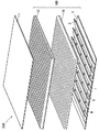
図1は、本発明に係る実施の形態の面発光装置100の構成を示す分解斜視図である。尚、図1には、面発光装置100の上にさらに液晶ユニット11を設けた、液晶表示装置の一部として、面発光装置100を表している。
Hereinafter, a surface light emitting device according to an embodiment of the present invention will be described with reference to the drawings.
FIG. 1 is an exploded perspective view showing a configuration of a surface
本実施の形態の面発光装置は、図1等に示すように、導光板を用いることなく、発光ダイオード5と反射体9が設けられた保持基板7と、プリズムシート13,15とを用いて構成されている。
As shown in FIG. 1 and the like, the surface light-emitting device of the present embodiment uses the holding substrate 7 provided with the light-
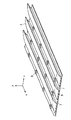
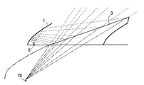
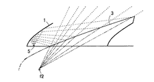
具体的には、本実施の形態の面発光装置において、図2Aに示すように、保持基板7には、複数の発光ダイオード5が、例えばマトリクス状に配列されており、各反射体9は、1つの列に配列された発光ダイオード5を一括して覆うように設けられている。この反射体9はそれぞれ、発光ダイオード5の発光面に対向する第1の面1(第1の反射面)と上面に当たる第2の面3とを有しており、反射体の第1の面1で反射された発光ダイオード5の光が隣の反射体9の第2の面に入射(照射)されるように配列されている。そして、反射体9の第2の面3は入射された発光ダイオードの光を上方にあるプリズムシート15の方向に反射させるように形成され、プリズムシート15及びプリズムシート13によって前方に出射される。
Specifically, in the surface light emitting device of the present embodiment, as shown in FIG. 2A, a plurality of
以下、本実施の形態の面発光装置における各要素について詳細に説明する。
<保持基板7>
保持基板7は、例えば、ガラエポ基板からなり、発光ダイオード5に電圧を印加するための電源配線が設けられた基板である。保持基板7の実装面には、発光ダイオード5が所定の配列で実装され、反射体9が所定の位置に取り付けられる。
保持基板として、アルミベース基板や銅ベース基板を用いても良い。アルミベース基板とは、アルミニウムの板に対して実装面側を絶縁膜で覆い、絶縁膜上に発光ダイオードパッケージ5のための配線パターンが設けられているものである。銅ベース基板はアルミベース基板のアルミニウムの部分が銅に置き換わったものを言う。
Hereinafter, each element in the surface light-emitting device of this Embodiment is demonstrated in detail.
<Holding substrate 7>
The holding substrate 7 is a substrate made of, for example, a glass epoxy substrate and provided with a power supply wiring for applying a voltage to the
An aluminum base substrate or a copper base substrate may be used as the holding substrate. The aluminum base substrate is a substrate in which a mounting surface side is covered with an insulating film with respect to an aluminum plate, and a wiring pattern for the light
<発光ダイオード>
発光ダイオード5は、ピンタイプ又は表面実装タイプのどちらのタイプでも使用することができるが、薄型化を考慮すると表面実装タイプの発光ダイオードを用いることが好ましい。また、発光ダイオードの発光色も適用される液晶表示装置の用途及び組み合わされる液晶ユニットの特性を考慮して種々の発光色のものを選択し得る。通常、バックライト用の面発光装置としては白色の光源が使用される。白色の発光ダイオードは、大別すると、特定の波長の発光ダイオードチップと蛍光体を組み合わせたタイプと、1つのパッケージの中にRGBの3つの発光ダイオードチップを設けたタイプがあるが、本実施の形態では、いずれのタイプであっても用いることができる。
また、本発明では、発光色が赤(R)、緑(G)、青(B)である3種類の発光ダイオード5を用いて、反射体9の第1の面及び第2の面によってそれら3色の光が混ざり合うように反射させて出射することで白色の面発光光源を実現することも可能である。
<Light emitting diode>
The light-
Further, in the present invention, three types of
また、発光ダイオード5は、図2に示すように、例えば、保持基板7上にZ方向及びX方向に一定間隔に配列(本明細書において、マトリクス配置という。)されるように実装される。尚、本発明において、発光ダイオード5の配列は、マトリクス配置に限定されるものではなく、例えば、Zには直線上に配列する一方、X方向には隣接間でZ座標を異ならせて配置(例えば、ジグザグに配置)してもよい。
As shown in FIG. 2, the light-
<反射体9>
反射体9は、その第1の面1でZ方向に配列された発光ダイオード5を一括して覆い、第2の面で隣接する反射体の第1の面から入射される光を上方に(プリズムシート15に向けて)反射させる。尚、実施の形態では、第2の面が鏡面の反射面である場合の例で説明するが、本発明では、入射される光を乱反射させるような反射面であっても良い。
反射体9の第1の面1は、その面で覆っている発光ダイオード5が出射する光を隣接する反射体9の第2の面3に向けて反射させる面である。
<
The
The first surface 1 of the
以上の反射体9は、Z方向に配列された発光ダイオード5を一括して覆うために、その長手方向がZ方向に一致するように、発光ダイオードが配列された各列に対応して保持基板7の実装面に取り付けられる。
尚、反射体9の第1の面1及び第2の面3の面形状の具体例、表面形態の具体例及びバリエーションについての詳細は後述する。
Since the
In addition, the specific example of the surface shape of the 1st surface 1 and the 2nd surface 3 of the
反射体の材料としては、大型ディスプレイへの応用が期待されていることから軽量材料であることが好ましい。また、第1の面及び第2の面は、光を反射するために、反射率の高い材料を用いることや、表面に金属コーティングすることが好ましい。具体的な材料として、樹脂として、アクリル樹脂、ポリカーボネート樹脂、非晶性ポリオレフィン樹脂、ポリスチレン樹脂、ノルボルネン系樹脂、シクロオレフィンポリマー(COP)、アクリロニトリル・ブタジエン・スチレン樹脂(ABS樹脂)等が挙げられる。反射体の材料としてAl等の金属を使用してもよい。Alを使用する場合、表面処理をしても使用できるが、鏡面処理をしても使用可能となる。 The material of the reflector is preferably a lightweight material since application to a large display is expected. In addition, the first surface and the second surface are preferably made of a highly reflective material or metal-coated on the surface in order to reflect light. Specific examples of the resin include acrylic resin, polycarbonate resin, amorphous polyolefin resin, polystyrene resin, norbornene resin, cycloolefin polymer (COP), acrylonitrile / butadiene / styrene resin (ABS resin), and the like. A metal such as Al may be used as a material for the reflector. When Al is used, it can be used even if it is surface-treated, but it can be used even if it is mirror-finished.
<プリズムシート13,15>
プリズムシート13,15は、例えば、ポリカーボネートからなるシートにプリズムパターンを形成したもの又はポリエステルからなるシートにアクリル樹脂からなるシートにプリズムパターンを形成したものを張り合わせたものからなり、反射体9の第2の面で反射された光の進行方向を、液晶ユニット11の法線方向に向けるものであり、プリズムシート13,15は、形成されているプリズムの方向が互いに直交するように配置されている。ここでは、プリズムシート15は、上面に、断面形状が三角形である複数のプリズムがZ方向に形成されており、第2の面3で反射された光のうちのXY面内成分の進行方向を液晶ユニット11の法線方向に向ける。
また、プリズムシート15は、上面に、断面形状が三角形である複数のプリズムがX方向に形成されており、第2の面3で反射された光のうちのYZ面内成分の進行方向を液晶ユニット11の法線方向に向ける。
これにより、第2の面3で反射された光は、プリズムシート13,15を通過することで、液晶ユニット11の液晶ユニットの法線方向に向けられる。
<
The
The
Thus, the light reflected by the second surface 3 passes through the
本発明に係る実施の形態の面発光装置は、以上のような構成により、導光板を使用することなく、実質的に点光源と見なされる発光ダイオードの光を拡げて面発光させるものである。この実施の形態の面発光装置では、例えば、反射体9の形状、特に、第1の面1と第2の面3の面形状と大きさ、反射体9の隣接間の間隔などを適切な形状、配置とすることにより、発光ダイオードの発光を効果的に面発光させかつ発光面における光量分布を均一にできる。
The surface light-emitting device according to the embodiment of the present invention is configured to emit light from a light-emitting diode that is substantially regarded as a point light source without using a light guide plate. In the surface light emitting device of this embodiment, for example, the shape of the
<各要素の形状、個数及び相互の配置>
本実施の形態において、使用する発光ダイオードの個数は、バックライト光源の発光面の大きさと、求められている輝度等に基づいて設定する。
個数を設定したら、保持基板7の実装面における、発光ダイオードの配列位置を設定する。ここで、発光ダイオードは、等間隔に配置することが好ましい。
<Shape, number and mutual arrangement of each element>
In the present embodiment, the number of light emitting diodes to be used is set based on the size of the light emitting surface of the backlight light source, the required luminance, and the like.
After the number is set, the arrangement position of the light emitting diodes on the mounting surface of the holding substrate 7 is set. Here, the light emitting diodes are preferably arranged at equal intervals.
反射体9の第1の面1は、上述したように、好ましくは、そこで反射した光を実質的に全て隣接する反射体9の第2の面に入力させるものであるから、その面形状及び発光ダイオードの発光面との相対位置は、隣接する反射体9の第2の面の位置、大きさ及び形状を考慮して設定される。
As described above, the first surface 1 of the
反射体9の第2の面3は、その面で反射した第1の面1からの光をプリズムシート15,13に入射させるものであり、当該第1の面1の形状及び第1の面1の位置を考慮して設定されるものであることは言うまでもないが、さらに、他の反射体9の第2の面との関係も考慮して、形状、大きさ及び位置を設定する。すなわち、複数の反射体の第2の面3で反射された光が、プリズムシート15,13に入射される時点のXZ平面内において光量分布が均一になるように第2の面3の形状と相対位置を設定すると、均一な面発光が可能な面発光装置が実現できる。尚、第2の反射面3はその端が発光ダイオード5の端まで達していても良い。
The second surface 3 of the
例えば、発光中心軸近傍に出射される光の強度が高く、発光中心軸から離れるにしたがって(発光中心軸との角度が大きくなるにしたがって)光の強度が減衰するような指向特性を持った発光ダイオードを用いた場合、以下のようにして、均一な面発光が実現できる。 For example, light emission with a directional characteristic in which the intensity of light emitted in the vicinity of the light emission center axis is high and the light intensity decreases as the distance from the light emission center axis increases (the angle with respect to the light emission center axis increases) When a diode is used, uniform surface emission can be realized as follows.
第1の方法.
上述したように、発光ダイオードから出射した光は、第1の面1と第2の面3で2回反射された後、プリズムシート15に到達する。そこで、発光ダイオードから出射される発光中心軸近傍の強度が高い光の広がりを、発光中心軸から離れた比較的強度の低い光に比較して大きくするように第1の面1と第2の面3の各面形状及び相対位置を設定する。すなわち、発光ダイオードの指向特性を考慮して、発光ダイオードの出射光がプリズムシート面に均一な光量分布で照射されるように、第1の面1と第2の面3の各面形状及び相対位置を設定すると、均一な面発光が実現できる。
First method.
As described above, the light emitted from the light emitting diode is reflected twice by the first surface 1 and the second surface 3 and then reaches the
第2の方法.
また、隣接する第2の面から反射される光がプリズムシート15に到達する際に重なるようにして光量分布の均一化を図ってもよい。
例えば、隣接する一方の第2の面から反射される光の発光中心軸から離れた強度の低い光と、他方の第2の面から反射される光の発光中心軸から離れた強度の低い光が重なり合って光量を補完しあうように、第1の面1と第2の面3の各面形状及び相対位置を設定する。このようにしても、均一な面発光が実現できる。
さらに本発明では、第1の方法と第2の方法を組み合わせて均一な面発光を実現してもよい。
Second method.
Further, the light amount distribution may be made uniform by overlapping when the light reflected from the adjacent second surface reaches the
For example, light with low intensity separated from the emission center axis of light reflected from one adjacent second surface and light with low intensity separated from the emission center axis of light reflected from the other second surface The surface shapes and relative positions of the first surface 1 and the second surface 3 are set so that the two overlap each other and complement the amount of light. Even in this way, uniform surface light emission can be realized.
Furthermore, in the present invention, uniform surface light emission may be realized by combining the first method and the second method.
次に、第1の面1及び第2の面3の面形状について説明する。
本実施の形態の面発光装置において、第1の面1及び第2の面3の面は、上述の機能が実現できる面であれば、平面であっても曲面であってもよい。しかしながら、均一な面発光を実現するためには、発光ダイオードから出射方向に応じて光の拡散度合いを調整しえる曲面であることが好ましい。本実施の形態において、曲面とする場合には、例えば、放物柱面の一部、双曲柱面の一部又は楕円柱面の一部により構成することができるし、さらには球面であっても良い。このような曲面を用いると光学設計を容易にできる。
Next, the surface shapes of the first surface 1 and the second surface 3 will be described.
In the surface light emitting device of the present embodiment, the surfaces of the first surface 1 and the second surface 3 may be flat or curved as long as the above functions can be realized. However, in order to realize uniform surface light emission, it is preferable that the curved surface be capable of adjusting the degree of light diffusion from the light emitting diode according to the emission direction. In the present embodiment, in the case of a curved surface, for example, it may be configured by a part of a parabolic column surface, a part of a hyperbolic column surface, or a part of an elliptical column surface, or a spherical surface. May be. If such a curved surface is used, optical design can be facilitated.
ここで、放物柱面とは、基準面からの距離とその基準面に平行な焦点軸からの距離(焦点軸に直交する面内における距離)が、等しい点の集まりとして定義される曲面である。また、双曲柱面とは、互いに平行な2つの焦点軸からの距離(焦点軸に直交する面内における距離)の差が一定である点の集まりとして定義される曲面である。楕円柱面とは互いに平行な2つの焦点軸からの距離(焦点軸に直交する面内における距離)の和が一定である点の集まりとして定義される面である。
すなわち、放物柱面では、任意のxy平面において断面が放物線であり、
双曲柱面では、任意のxy平面において断面が双曲線であり、楕円柱面では、任意のxy平面において断面が楕円である。
Here, the parabolic column surface is a curved surface defined as a collection of points where the distance from the reference plane and the distance from the focal axis parallel to the reference plane (the distance in the plane orthogonal to the focal axis) are equal. is there. The hyperbolic cylinder surface is a curved surface defined as a collection of points having a constant difference in distance from two parallel focal axes (distance in a plane perpendicular to the focal axis). An elliptic cylinder surface is a surface defined as a collection of points with a constant sum of distances from two parallel focal axes (distances in a plane perpendicular to the focal axis).
That is, in the parabolic column surface, the cross section is a parabola in an arbitrary xy plane,
In the hyperbolic cylinder surface, the cross section is a hyperbola in an arbitrary xy plane, and in the elliptic cylinder surface, the cross section is an ellipse in an arbitrary xy plane.
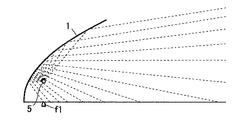
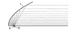
図3A〜図3Cには、それぞれ第1の面1を放物柱面にした場合について示している。また、図3Cでは、発光ダイオード5を焦点軸f1上に配置した場合を示し、図3Aには、発光ダイオード5を焦点軸上よりも第1の面に近づけて配置した場合を示している。図3Bは、それらの中間に発光ダイオード5を配置した例である。図3A〜図3Cから明らかなように、第1の面1が同じ形状であっても第1の面1に対する発光ダイオード5の位置を変更することにより、第1の面1で反射された後の光の広がりを制御することができることがわかる。
3A to 3C show cases where the first surface 1 is a parabolic column surface. 3C shows a case where the
例えば、焦点軸上に発光ダイオード5を配置した図3Cの場合では、発光ダイオードの光は反射された後、平行になる。このようにすると、第2の面の形状設計が容易になるとともに、隣接する反射体間の相対位置の誤差による影響を少なくできる。
また、発光ダイオード5を第1の面に近づけると、発光ダイオードの光は反射後の拡散範囲を広くできる。
For example, in the case of FIG. 3C in which the
Further, when the
図4A及び図4Bには、第1の面1と第2の面3をいずれも双曲柱面とした場合について示している。この図4A及び図4Bではいずれも発光ダイオード5は、第1の面の焦点軸上に配置している。第1の面を双曲柱面とした場合であっても、第1の面1を放物柱面にした場合と同様、第1の面に対する発光ダイオードの相対位置を変更することにより、第1の面で反射された後の光の広がり度合いを制御できる。
図4Aと図4Bの間では、第2の面における焦点軸f2の位置が異なっている。具体的には、図4Aでは、図4Bの第2の面より、焦点軸から離れた部分にある双曲柱面の一部利用して第2の面が構成されており、図4Bに示す第2の面は、図4Aに示す第2の面より曲率が大きく、図4Aに示す第2の面の方がより平面に近い曲面になっている。その結果、第2の面で反射された後の光の広がりは、図4Bの方が大きくなっている。
4A and 4B show a case where both the first surface 1 and the second surface 3 are hyperbolic column surfaces. 4A and 4B, the
4A and 4B, the position of the focal axis f2 on the second surface is different. Specifically, in FIG. 4A, the second surface is configured by using a part of the hyperbolic column surface that is located farther from the focal axis than the second surface in FIG. 4B, and is shown in FIG. 4B. The second surface has a larger curvature than the second surface shown in FIG. 4A, and the second surface shown in FIG. 4A is a curved surface that is closer to a flat surface. As a result, the spread of the light after being reflected by the second surface is larger in FIG. 4B.
このように、双曲柱面や放物柱面を用いて、焦点軸の位置及び発光ダイオードの配置位置等により、反射方向及び光の拡散を種々変更できるので、それらのパラメータを逐次変更しながら最適化することにより、均一な面発光を実現できる。
また、楕円柱面を用いた場合も同様に、焦点軸の位置、発光ダイオードの配置位置等によって均一な面発光が可能である。
In this way, by using the hyperbolic column surface and the parabolic column surface, the reflection direction and the light diffusion can be variously changed according to the position of the focal axis and the arrangement position of the light emitting diode, etc. By optimizing, uniform surface emission can be realized.
Similarly, when an elliptic cylinder surface is used, uniform surface light emission is possible depending on the position of the focal axis, the position of the light emitting diode, and the like.
尚、本発明では、第1の面及び第2の面は、ミラーボールのような、複数の平面の集合体からなる擬似的な曲面であってもよい。 In the present invention, the first surface and the second surface may be pseudo curved surfaces made of an assembly of a plurality of planes such as mirror balls.
以上、詳細に説明したように、本発明に係る実施の形態の面発光装置は、以下のような特有の効果を有する。
第1に、本発明に係る実施の形態の面発光装置は、複数の反射体9を用いて、点光源である発光ダイオードの光を拡げているので、導光板を用いることなく面発光させることができ、発光面の面積が大きくかつ薄型で軽量の面発光装置を実現できる。
As described above in detail, the surface light emitting device according to the embodiment of the present invention has the following specific effects.
1stly, since the surface emitting device of embodiment which concerns on this invention has spread the light of the light emitting diode which is a point light source using the
また、本発明に係る実施の形態の面発光装置では、発光ダイオードを2次元的(例えば、マトリクス状)に配列することができるので、構造に起因する制約を受けることなく、要求される輝度に応じて発光ダイオードの個数を設定することができ、高い輝度の面発光を容易に実現できる。
すなわち、導光板を使用する従来のタイプでは、導光板の側面に発光ダイオードを配列することになるので、使用することができる発光ダイオードの数が制限される。
従って、発光ダイオードを用いた高輝度でかつ大型のバックライト光源を容易に構成でき、大型の液晶表示装置に利用し得る面発光装置を提供できる。
Further, in the surface light emitting device according to the embodiment of the present invention, since the light emitting diodes can be arranged two-dimensionally (for example, in a matrix), the required luminance can be obtained without being restricted by the structure. Accordingly, the number of light emitting diodes can be set, and surface emission with high luminance can be easily realized.
That is, in the conventional type using a light guide plate, light emitting diodes are arranged on the side surface of the light guide plate, so that the number of light emitting diodes that can be used is limited.
Accordingly, a high-luminance and large-sized backlight light source using a light-emitting diode can be easily configured, and a surface light-emitting device that can be used for a large-sized liquid crystal display device can be provided.
さらに、本発明に係る実施の形態の面発光装置では、第1の面1と第2の面3の各面形状及び相対位置により、均一な面発光をさせることができる。
特に、本実施の形態の構造では、第1の面1と第2の面3により2段階で反射させて発光ダイオードの光を拡散させているので、点光源である発光ダイオードを光源として用いた場合であっても、容易に2次元的な面に拡げることができる。
また、発光ダイオードは、消費電力が小さく長寿命であることから、発光ダイオードを光源として使用した場合には、低消費電力でかつ寿命の長い面発光光源が実現できる。
Furthermore, in the surface light emitting device according to the embodiment of the present invention, uniform surface light emission can be performed by the surface shapes and relative positions of the first surface 1 and the second surface 3.
In particular, in the structure of the present embodiment, the light of the light emitting diode is diffused by being reflected by the first surface 1 and the second surface 3 in two stages, so that the light emitting diode that is a point light source is used as the light source. Even in this case, it can be easily expanded to a two-dimensional surface.
In addition, since the light emitting diode has low power consumption and long life, when the light emitting diode is used as a light source, a surface emitting light source with low power consumption and long life can be realized.
以上、実施の形態の面発光装置に基づいて、本発明について説明したが、本発明は上記実施の形態に限定されるものではなく、発明の範囲内において種々の変形が可能である。
以下、代表的な変形例について説明する。
The present invention has been described above based on the surface light emitting device of the embodiment. However, the present invention is not limited to the above embodiment, and various modifications can be made within the scope of the invention.
Hereinafter, typical modifications will be described.
変形例1.
本発明に係る実施の形態の面発光装置では、第2の面3を滑らかな反射面(鏡面)としたが、本発明では、第2の面が入射される光を散乱させる散乱面(例えば、粗面)であってもよい。
このように構成された変形例1の面発光装置を、例えば、液晶表示装置以外の用途(発光面に対して直交する方向に出射する必要がない用途)に用いる場合には、プリズムシートを用いることなく構成することが可能であり、構成を簡単にできる。
Modification 1
In the surface light emitting device according to the embodiment of the present invention, the second surface 3 is a smooth reflecting surface (mirror surface). However, in the present invention, the second surface 3 is a scattering surface that scatters incident light (for example, , Rough surface).
When the surface light emitting device of Modification 1 configured as described above is used for, for example, a use other than the liquid crystal display device (use that does not need to emit light in a direction orthogonal to the light emitting surface), a prism sheet is used. It can be configured without any problem, and the configuration can be simplified.
変形例2.
実施の形態の面発光装置では、マトリクス状に配列した発光ダイオードを用いたが、本発明はこれに限られるものではなく、発光ダイオードに代えて、同じく点光源であるハロゲンランプやHIDランプを用いてもよい。
また、本発明では、発光ダイオードに代えて、線光源である、冷陰極蛍光ランプ(CCFL)や熱陰極蛍光ランプ(HCFL)、外部電極蛍光ランプ、有機EL、無機ELなどを用いて構成することもできる。
さらに、本発明では、光源として、点光源と線光源を組み合わせて用いてもよい。
Modification 2
In the surface light emitting device of the embodiment, the light emitting diodes arranged in a matrix are used, but the present invention is not limited to this, and instead of the light emitting diodes, a halogen lamp or an HID lamp which is also a point light source is used. May be.
Further, in the present invention, instead of the light emitting diode, a line light source such as a cold cathode fluorescent lamp (CCFL), a hot cathode fluorescent lamp (HCFL), an external electrode fluorescent lamp, an organic EL, an inorganic EL, or the like is used. You can also.
Furthermore, in this invention, you may use combining a point light source and a line light source as a light source.
変形例3.
以上の実施の形態の面発光装置では、第1の面1と第2の面3とを備えた反射体を用いて構成したが、第1の面1を備えた構造体と第2の面3を備えた構造体を別体の構造体としてもよい。以上のようにしても実施の形態と同様の作用効果が得られる。
Modification 3
In the surface light-emitting device of the above embodiment, although it comprised using the reflector provided with the 1st surface 1 and the 2nd surface 3, the structure provided with the 1st surface 1, and the 2nd surface 3 may be a separate structure. Even if it does as mentioned above, the effect similar to embodiment is obtained.
変形例4.
本実施の形態では、1列に配列された複数の発光ダイオードを一括して覆う反射体を設けたが、本発明はこれに限られるものではなく、1つの発光ダイオードに対して1つの反射体を設けるようにしてもよい。
以上、代表的な変形例を挙げたが、本発明はこれらの実施の形態及び変形例に限定されるものではなく、本発明の範囲内においてさらに種々の変形が可能である。
Modification 4
In the present embodiment, a reflector that collectively covers a plurality of light emitting diodes arranged in a row is provided. However, the present invention is not limited to this, and one reflector is provided for one light emitting diode. May be provided.
As mentioned above, although the typical modification was given, this invention is not limited to these embodiment and modification, Furthermore, a various deformation | transformation is possible within the scope of the present invention.
本発明の実施例1の構成要素を以下に詳述する。
保持基板7としてはアルミベース基板を使用する。
反射体9は、材料として白色のポリカーボネート樹脂を使用する。第1の面1に鏡面加工を施し、第2の面3にブラスト加工を施す。反射体の形状としては、図4Aのように第1の面1と第2の面3を共に双曲柱面として形成する。光源としての発光ダイオードは第1の面1の焦点に配置する。反射体の大きさは、短手方向(図2のx軸方向)の長さを32mm、長手方向(図2のz軸方向)の長さを200mmとする。1反射体が覆う発光ダイオード5の数を4つとする。短手方向に15の反射体9を配置し、長手方向に4の反射体9を配置する、すなわち縦15×横4(15行4列)に形成する。さらに反射体の直上に2枚のプリズムシートをプリズム面を上向きに直行させて配置する。このようにして40inch用の面発光装置が完成する。
1発光ダイオード5当たり、動作電圧(Vf)を4.3V、動作電流(If)を350mAで駆動させる。このように配置した面発光装置は一部に極端に明るい異常発光等は見られず、略6000cd/m2となる。
The components of the first embodiment of the present invention will be described in detail below.
An aluminum base substrate is used as the holding substrate 7.
The
The driving voltage (Vf) is driven at 4.3 V and the operating current (If) at 350 mA per one
本発明の実施例2の構成要素を以下に詳述する。以下に言及しない部分に関しては実施例1の構成と同様とする。
反射体9は、材料としてアクリル樹脂を使用する。図3Cのように第1の面1を放物柱面とし、且つ、Agを蒸着して鏡面化させる。第2の面3は平面とし、且つ、白色のポリカーボネート製の拡散性のシートを配置する。
このような構成を有し、他の部分は実施例1と同様の構成とする。駆動させた場合、実施例1と同程度の特性が得られる。
The components of the second embodiment of the present invention are described in detail below. The parts not mentioned below are the same as those of the first embodiment.
The
Having such a configuration, the other parts are the same as those in the first embodiment. When driven, the same characteristics as in Example 1 can be obtained.
本発に係る面発光装置は、主として、チャネルレターやコンピュータ、ワードプロセッサ、テレビジョン等の画像表示に用いる液晶表示素子のバックライト光源などに利用されるが、他の用途にも幅広く適用し得る。 The surface emitting device according to the present invention is mainly used for a backlight light source of a liquid crystal display element used for image display such as a channel letter, a computer, a word processor, and a television, but can be widely applied to other applications.
1・・・第1の面
3・・・第2の面
5・・・発光ダイオード
7・・・保持基板
9・・・反射体
11・・・液晶ユニット
13,15・・・プリズムシート
100・・・面発光装置
200・・・液晶表示装置
DESCRIPTION OF SYMBOLS 1 ... 1st surface 3 ...
Claims (14)
それぞれ前記光源を覆う第1の面と照射される光を反射させる第2の面とを有する複数の反射体と、前記複数の光源と前記複数の反射体とが設けられた基板と、を備え、
前記反射体はそれぞれ、当該第1の面で前記光源から出射される光を隣接する反射体に設けられた第2の面に照射させるように配置され、該第2の面で反射された光を出射することを特徴とする面発光装置。 Multiple light sources;
A plurality of reflectors having a second surface for reflecting the light emitted from the first surface, each covering the light source, the plurality of light sources and the plurality of reflectors and substrate provided with the Prepared,
Each of the reflectors is disposed so as to irradiate light emitted from the light source on the first surface to a second surface provided on an adjacent reflector, and is reflected on the second surface. A surface light-emitting device that emits light.
Priority Applications (1)
| Application Number | Priority Date | Filing Date | Title |
|---|---|---|---|
| JP2005371974A JP4635863B2 (en) | 2005-01-19 | 2005-12-26 | Surface emitting device |
Applications Claiming Priority (2)
| Application Number | Priority Date | Filing Date | Title |
|---|---|---|---|
| JP2005011480 | 2005-01-19 | ||
| JP2005371974A JP4635863B2 (en) | 2005-01-19 | 2005-12-26 | Surface emitting device |
Publications (2)
| Publication Number | Publication Date |
|---|---|
| JP2006228710A JP2006228710A (en) | 2006-08-31 |
| JP4635863B2 true JP4635863B2 (en) | 2011-02-23 |
Family
ID=36989869
Family Applications (1)
| Application Number | Title | Priority Date | Filing Date |
|---|---|---|---|
| JP2005371974A Expired - Fee Related JP4635863B2 (en) | 2005-01-19 | 2005-12-26 | Surface emitting device |
Country Status (1)
| Country | Link |
|---|---|
| JP (1) | JP4635863B2 (en) |
Families Citing this family (9)
| Publication number | Priority date | Publication date | Assignee | Title |
|---|---|---|---|---|
| KR101318302B1 (en) * | 2006-09-12 | 2013-10-16 | 삼성디스플레이 주식회사 | Backlight assembly and display apparatus having the same |
| US7719633B2 (en) | 2006-12-26 | 2010-05-18 | Citizen Electronics Co., Ltd. | Light source apparatus |
| JP4716435B2 (en) * | 2007-03-02 | 2011-07-06 | シチズン電子株式会社 | Light source device and display device provided with light source device |
| JP4751367B2 (en) * | 2007-05-18 | 2011-08-17 | シチズン電子株式会社 | Light source device and display device provided with light source device |
| JP5072069B2 (en) | 2007-03-05 | 2012-11-14 | シチズン電子株式会社 | Light source device |
| CN101680610B (en) | 2007-05-10 | 2012-03-07 | 夏普株式会社 | Illuminating device, display device having it, and television receiver |
| RU2011144379A (en) * | 2009-04-02 | 2013-05-10 | ФИЛИПС ЛЮМИЛЕДС ЛАЙТИНГ КОМПАНИ, ЭлЭлСи | Backlight for LCD |
| JP2012134309A (en) * | 2010-12-21 | 2012-07-12 | Panasonic Corp | Ultraviolet radiation apparatus |
| CN106134171B (en) * | 2014-03-17 | 2019-06-14 | 三菱电机株式会社 | Lighting device and image reading device |
Family Cites Families (2)
| Publication number | Priority date | Publication date | Assignee | Title |
|---|---|---|---|---|
| JP2001312916A (en) * | 2000-02-24 | 2001-11-09 | Sony Corp | Surface light source device |
| JP2004111189A (en) * | 2002-09-18 | 2004-04-08 | Asahi Matsushita Electric Works Ltd | Light guide plate device |
-
2005
- 2005-12-26 JP JP2005371974A patent/JP4635863B2/en not_active Expired - Fee Related
Also Published As
| Publication number | Publication date |
|---|---|
| JP2006228710A (en) | 2006-08-31 |
Similar Documents
| Publication | Publication Date | Title |
|---|---|---|
| EP1684111B1 (en) | Surface light emitting apparatus | |
| JP5290279B2 (en) | Lighting system, lighting fixture and backlighting unit | |
| US7506998B2 (en) | Illumination system | |
| US7341358B2 (en) | Illumination apparatus | |
| JP4368075B2 (en) | Surface lighting device | |
| JP5390604B2 (en) | Collimated light engine | |
| JP2021517351A (en) | Lighting device | |
| US20080231772A1 (en) | Flat panel display and fabrication method thereof | |
| US20080278659A1 (en) | Light-Guide Plate, Method of Manufacturing the Same and Display Apparatus Having the Same | |
| JP2006031941A (en) | Planar light source unit | |
| JP5450778B2 (en) | Edge light type surface light source device and illumination device | |
| JP2012216747A (en) | Light-emitting device, lighting device and display | |
| JP2006294618A (en) | Luminescent panel | |
| WO2013005487A1 (en) | Light emitting device and display device | |
| US6913378B2 (en) | Direct-lighting type back light unit | |
| CN111164772B (en) | Very wide distributed Light Emitting Diode (LED) lens for thin direct type backlight | |
| KR20190021522A (en) | Light guide plate and backlight unit having the same | |
| US20070147037A1 (en) | Super slim LCD backlight device using uniforming chamber | |
| JP4635863B2 (en) | Surface emitting device | |
| JP2007234385A (en) | Backlight device | |
| JP2009506501A (en) | Direct type backlight with light source for bifunctional spectrometer | |
| CN102042558B (en) | Color mixing lens and liquid crystal display having the same | |
| JP2010212083A (en) | Light source unit, lighting system, and liquid crystal display device | |
| KR101798599B1 (en) | Luminous flux control member and back light unit using the same | |
| JP4848534B2 (en) | Planar light source |
Legal Events
| Date | Code | Title | Description |
|---|---|---|---|
| RD03 | Notification of appointment of power of attorney |
Free format text: JAPANESE INTERMEDIATE CODE: A7423 Effective date: 20070816 |
|
| A621 | Written request for application examination |
Free format text: JAPANESE INTERMEDIATE CODE: A621 Effective date: 20080926 |
|
| A977 | Report on retrieval |
Free format text: JAPANESE INTERMEDIATE CODE: A971007 Effective date: 20100427 |
|
| A131 | Notification of reasons for refusal |
Free format text: JAPANESE INTERMEDIATE CODE: A131 Effective date: 20100506 |
|
| A521 | Request for written amendment filed |
Free format text: JAPANESE INTERMEDIATE CODE: A523 Effective date: 20100628 |
|
| TRDD | Decision of grant or rejection written | ||
| A01 | Written decision to grant a patent or to grant a registration (utility model) |
Free format text: JAPANESE INTERMEDIATE CODE: A01 Effective date: 20101026 |
|
| A01 | Written decision to grant a patent or to grant a registration (utility model) |
Free format text: JAPANESE INTERMEDIATE CODE: A01 |
|
| A61 | First payment of annual fees (during grant procedure) |
Free format text: JAPANESE INTERMEDIATE CODE: A61 Effective date: 20101108 |
|
| FPAY | Renewal fee payment (event date is renewal date of database) |
Free format text: PAYMENT UNTIL: 20131203 Year of fee payment: 3 |
|
| R150 | Certificate of patent or registration of utility model |
Ref document number: 4635863 Country of ref document: JP Free format text: JAPANESE INTERMEDIATE CODE: R150 Free format text: JAPANESE INTERMEDIATE CODE: R150 |
|
| R250 | Receipt of annual fees |
Free format text: JAPANESE INTERMEDIATE CODE: R250 |
|
| R250 | Receipt of annual fees |
Free format text: JAPANESE INTERMEDIATE CODE: R250 |
|
| R250 | Receipt of annual fees |
Free format text: JAPANESE INTERMEDIATE CODE: R250 |
|
| R250 | Receipt of annual fees |
Free format text: JAPANESE INTERMEDIATE CODE: R250 |
|
| R250 | Receipt of annual fees |
Free format text: JAPANESE INTERMEDIATE CODE: R250 |
|
| R250 | Receipt of annual fees |
Free format text: JAPANESE INTERMEDIATE CODE: R250 |
|
| R250 | Receipt of annual fees |
Free format text: JAPANESE INTERMEDIATE CODE: R250 |
|
| R250 | Receipt of annual fees |
Free format text: JAPANESE INTERMEDIATE CODE: R250 |
|
| R250 | Receipt of annual fees |
Free format text: JAPANESE INTERMEDIATE CODE: R250 |
|
| R250 | Receipt of annual fees |
Free format text: JAPANESE INTERMEDIATE CODE: R250 |
|
| LAPS | Cancellation because of no payment of annual fees |