JP4635604B2 - Method for manufacturing exposure mask blank, exposure mask, method for manufacturing color filter for liquid crystal display device, and color filter for liquid crystal display device - Google Patents
Method for manufacturing exposure mask blank, exposure mask, method for manufacturing color filter for liquid crystal display device, and color filter for liquid crystal display device Download PDFInfo
- Publication number
- JP4635604B2 JP4635604B2 JP2004375913A JP2004375913A JP4635604B2 JP 4635604 B2 JP4635604 B2 JP 4635604B2 JP 2004375913 A JP2004375913 A JP 2004375913A JP 2004375913 A JP2004375913 A JP 2004375913A JP 4635604 B2 JP4635604 B2 JP 4635604B2
- Authority
- JP
- Japan
- Prior art keywords
- liquid crystal
- crystal display
- color filter
- display device
- exposure mask
- Prior art date
- Legal status (The legal status is an assumption and is not a legal conclusion. Google has not performed a legal analysis and makes no representation as to the accuracy of the status listed.)
- Expired - Fee Related
Links
Images


Landscapes
- Liquid Crystal (AREA)
- Preparing Plates And Mask In Photomechanical Process (AREA)
- Exposure And Positioning Against Photoresist Photosensitive Materials (AREA)
Description
本発明は、液晶表示装置用カラーフィルタの柱状スペーサーとオーバーコート層を一括で形成するための露光マスク、露光マスク用ブランク及び柱状スペーサーとオーバーコート層を一括で形成した液晶表示装置用カラーフィルタに関する。 The present invention relates to an exposure mask for collectively forming columnar spacers and overcoat layers of a color filter for liquid crystal display devices, an exposure mask blank, and a color filter for liquid crystal display devices in which columnar spacers and overcoat layers are formed in a lump. .
従来の液晶表示装置では、スペーサーと呼ばれるガラスまたは合成樹脂のビーズスペーサーと呼ばれる球状スペーサーが使われてきた。しかし、このビーズスペーサーは位置が定まっておらず、液晶表示装置基板上の表示領域にも存在する為、ビーズスペーサーによる、光の散乱・透過及びビーズスペーサー近傍の配向の乱れにより、液晶表示装置の表示品位が低下するという問題を有している。
このため、従来の球状スペーサーの限界が指摘され、定位置への配置形成が可能な柱状スペーサーを用いた液晶表示装置用カラーフィルタが提案されている(例えば、特許文献1参照。)。
In conventional liquid crystal display devices, glass spacers called spacers or spherical spacers called synthetic resin bead spacers have been used. However, since the position of the bead spacer is not fixed and is also present in the display area on the liquid crystal display device substrate, the bead spacer causes scattering and transmission of light and disturbance of the alignment in the vicinity of the bead spacer. There is a problem that the display quality deteriorates.
For this reason, the limitation of the conventional spherical spacer is pointed out, and a color filter for a liquid crystal display device using a columnar spacer that can be arranged at a fixed position has been proposed (for example, see Patent Document 1).
また、ガラス基板大型化の動向から液晶表示装置製造工程においては、セルギャップの均一性確保が最大の課題となり、液晶注入工程短縮の必要性から、液晶滴下法が今後、主流になると考えられているが、こうした点に対応するには柱状スペーサー付きカラーフィルタが必須とされている。
更に、この柱状スペーサーに加えカラーフィルタに付与されるオーバーコート層とは、液晶表示装置の広視野角化に対応するため平坦化、イオンバリアを目的とした保護層である。
In addition, due to the trend toward larger glass substrates, securing the cell gap uniformity is the biggest issue in the liquid crystal display manufacturing process, and the liquid crystal dropping method is expected to become the mainstream in the future due to the necessity of shortening the liquid crystal injection process. However, a color filter with columnar spacers is essential to cope with these points.
Further, the overcoat layer applied to the color filter in addition to the columnar spacer is a protective layer for the purpose of flattening and ion barrier in order to cope with the wide viewing angle of the liquid crystal display device.
液晶表示装置用カラーフィルタの柱状スペーサーもオーバーコート層も感光性樹脂を用いたフォトリソ工程で形成される。図10にオーバーコート層と柱状スペーサーが形成された従来の液晶表示装置用カラーフィルタの一例を示す。
このオーバーコート層と柱状スペーサーは、まず、オーバーコート層73を形成した後に柱状スペーサー74が形成される。
このように、現状ではオーバーコート層と柱状スペーサーは、個別の材料と個別のプロセスを経て作製されている。そのため、装置コストを圧迫し、カラーフィルタの製造原価に大きく影響を与えている。
Both the columnar spacer and the overcoat layer of the color filter for liquid crystal display devices are formed by a photolithography process using a photosensitive resin. FIG. 10 shows an example of a conventional color filter for a liquid crystal display device in which an overcoat layer and a columnar spacer are formed.
As for the overcoat layer and the columnar spacer, first, after the
Thus, at present, the overcoat layer and the columnar spacer are manufactured through individual materials and individual processes. For this reason, the cost of the apparatus is pressed and the manufacturing cost of the color filter is greatly affected.
従って、液晶表示装置における高速応答、大画面、広視野角化といった今後のトレンドに対応するためには、柱状スペーサー及びオーバーコート層を備えた液晶表示装置用カラーフィルタが求められることになるが、同時にこれらの普及のためには、性能だけでなく、価格の大幅な低減が必要である。
本発明は、上記問題点に鑑み考案されたもので、柱状スペーサーならびにオーバーコート層を備えた液晶表示装置用カラーフィルタを製造するにあたり、製造工程の簡略化を図るための工程及びその工程に使用する露光マスクを考案し、製造コスト低減化を図った液晶表示装置用カラーフィルタの製造方法を提供することを目的とする。 The present invention has been devised in view of the above problems, and in manufacturing a color filter for a liquid crystal display device having a columnar spacer and an overcoat layer, and a process for simplifying the manufacturing process and its use An object of the present invention is to provide a method for manufacturing a color filter for a liquid crystal display device in which an exposure mask is devised and the manufacturing cost is reduced.
本発明に於いて上記課題を達成するために、まず請求項1においては、液晶表示装置用カラーフィルタの柱状スペーサーとオーバーコート層を一括形成するための露光マスク用ブランクであって、ガラス基板上に紫外線透過率制御機能を有する半透過膜と紫外線遮蔽効果を有する遮光膜とが形成されていることを特徴とする露光マスク用ブランクとしたものである。 In order to achieve the above object in the present invention, first, in claim 1, a blank for an exposure mask for collectively forming columnar spacers and an overcoat layer of a color filter for a liquid crystal display device, on a glass substrate The exposure mask blank is characterized in that a semi-transmissive film having an ultraviolet transmittance control function and a light-shielding film having an ultraviolet shielding effect are formed.
また、請求項2においては、前記半透過膜の紫外光に対する透過率は、波長300nmで5%以下、波長380nmでは45%以上であることを特徴とする請求項1に記載の露光マスク用ブランクとしたものである。 The exposure mask blank according to claim 1, wherein the translucent film has a transmittance for ultraviolet light of 5% or less at a wavelength of 300 nm and 45% or more at a wavelength of 380 nm. It is what.
また、請求項3においては、前記半透過膜は酸化インジウムと酸化錫との化合物膜からなるITO膜からなり、前記酸化錫が原子数比で10%以下含有されていることを特徴とする請求項1または2に記載の露光マスク用ブランクとしたものである。 According to a third aspect of the present invention, the semi-transmissive film is made of an ITO film made of a compound film of indium oxide and tin oxide, and the tin oxide is contained in an atomic ratio of 10% or less. Item 3. The exposure mask blank according to Item 1 or 2.
また、請求項4においては、前記半透過膜は、キャリアガスと酸素ガスを用いた反応性スパッタリングにより成膜され、前記酸素ガス流量の割合が総流量に対して0.6%以上になっていることを特徴とする請求項1乃至3のいずれか一項に記載の露光マスク用ブランクの製造方法としたものである。 According to a fourth aspect of the present invention, the semipermeable membrane is formed by reactive sputtering using a carrier gas and an oxygen gas, and the ratio of the oxygen gas flow rate is 0.6% or more with respect to the total flow rate. It is set as the manufacturing method of the blank for exposure masks as described in any one of Claims 1 thru | or 3 characterized by the above-mentioned.
また、請求項5においては、請求項1乃至3に記載の露光マスク用ブランクを用いて作製したことを特徴とする露光マスクとしたものである。 According to a fifth aspect of the present invention, there is provided an exposure mask produced using the exposure mask blank according to any one of the first to third aspects.
また、請求項6においては、ガラス基板上に少なくともブラックマトリクス、赤色フィルタ、青色フィルタ、緑色フィルタ、オーバーコート層、柱状スペーサーが形成されてなる液晶表示装置用カラーフィルタの製造方法において、請求項5に記載の露光マスクを用いて柱状スペーサーとオーバーコート層を一括露光にて形成することを特徴とする液晶表示装置用カラーフィルタの製造方法としたものである。 According to a sixth aspect of the present invention, in the method for producing a color filter for a liquid crystal display device, at least a black matrix, a red filter, a blue filter, a green filter, an overcoat layer, and a columnar spacer are formed on a glass substrate. A columnar spacer and an overcoat layer are formed by batch exposure using the exposure mask described in 1 above, and this is a method for producing a color filter for a liquid crystal display device.
さらにまた、請求項7においては、請求項6に記載の液晶表示装置用カラーフィルタの製造方法にて作製されたことを特徴とする液晶表示装置用カラーフィルタとしたものである。 Further, according to a seventh aspect of the present invention, there is provided a color filter for a liquid crystal display device produced by the method for producing a color filter for a liquid crystal display device according to the sixth aspect.
本発明の露光用マスクを用いて、液晶表示装置用カラーフィルタの柱状スペーサーとオーバーコート層を一括露光にて形成することにより、液晶表示装置用カラーフィルタの製造工程の簡略化を図ることができ、液晶表示装置用カラーフィルタの製造コストの低減につなげることができる。 By using the exposure mask of the present invention to form columnar spacers and an overcoat layer of a color filter for a liquid crystal display device by batch exposure, the manufacturing process of the color filter for the liquid crystal display device can be simplified. Thus, the manufacturing cost of the color filter for the liquid crystal display device can be reduced.
以下、本発明の実施の形態につき説明する。
図1は、露光マスクを作製するための本発明の露光マスク用ブランクの構成例を、図2は、液晶表示装置用カラーフィルタの柱状スペーサーとオーバーコート層を一括形成するための本発明の露光マスクの構成例を、図3は、本発明の露光マスクを用いて柱状スペーサーとオーバーコート層を一括形成した本発明の液晶表示装置用カラーフィルタの構成例をそれぞれ示す。
Hereinafter, embodiments of the present invention will be described.
FIG. 1 shows an example of the configuration of an exposure mask blank of the present invention for producing an exposure mask, and FIG. 2 shows the exposure of the present invention for collectively forming columnar spacers and an overcoat layer of a color filter for a liquid crystal display device. FIG. 3 shows a configuration example of a mask, and FIG. 3 shows a configuration example of a color filter for a liquid crystal display device of the present invention in which columnar spacers and an overcoat layer are collectively formed using the exposure mask of the present invention.
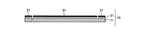
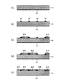
請求項1に係る本発明の露光マスク用ブランク10は、図1に示すように、石英基板等からなるガラス基板11上に、紫外線透過率制御機能を有する半透過膜21と、紫外線遮蔽効果を有するCr膜等からなる遮光膜31とで構成されている。
As shown in FIG. 1, the exposure mask blank 10 according to the first aspect of the present invention has, on a
請求項2に係る本発明の露光マスク用ブランク10aの半透過膜21の紫外光に対する透過率は、波長300nmで5%以下、波長380nmでは45%以上の透過率特性を持たせてある。
この半透過膜21のパターン露光における作用効果について、図4(a)〜(c)を用いて説明する。
図4(a)に示すガラス基板11上に波長300nmで5%以下、波長380nmでは45%以上の透過率特性を有する半透過膜21とCr膜等からなる遮光膜31とが形成された本発明の露光マスク用ブランク10をパターニング処理して、マスクパターンP1及びマスクパターンP2が形成された露光マスク10bを用いて、ガラス基板51上に形成されたネガレジスト72をパターン露光し(図4(b)参照)、現像処理して、ネガレジスト72の膜厚と同等でパターン化されたレジストパターン72aとネガレジスト72の膜厚よりも膜減りしたレジストパターン72bが得られる。
The transmittance of the
The effects of the
A book in which a
これは、マスクパターンP1からは通常の露光波長の露光光が照射され、マスクパターンP2から照射される露光光は、半透過膜21aにて300nmで5%以下、380nmで45%以上の透過率制御を行っているので、ネガレジスト72にマスクパターンP1とマスクターンP2で同じ露光量でパターン露光した場合マスクパターンP1では、ネガレジストが完全に硬化する露光条件になっているのでほぼレジスト厚相当のマスクパターン形状に応じたレジストパターン72aが、マスクパターンP2では、半透過膜21aにより露光光の波長選択と露光制御が行われるため、レジストパターン72aよりも膜厚が減少したレジストパターン72bが形成される。
このことから、本発明の露光用マスクを用いて一括露光することにより、1枚の露光マスクで高さの異なるレジストパターンを同時に得ることができる。
The mask pattern P 1 is irradiated with exposure light having a normal exposure wavelength, and the exposure light irradiated from the mask pattern P 2 is 5% or less at 300 nm and 45% or more at 380 nm in the
From this, it is possible to simultaneously obtain resist patterns having different heights with one exposure mask by performing batch exposure using the exposure mask of the present invention.
請求項3に係る本発明の露光マスク用ブランクは、半透過膜21が酸化インジウムと酸化錫の化合物膜からなるITO膜で構成されており、半透過膜21の光学特性(紫外光に対して、波長300nmで5%以下、波長380nmで45%以上の透過率特性)を満たすために、酸化錫が原子数比で10%以下含有されるようにしている。
In the exposure mask blank of the present invention according to claim 3, the
以下、本発明の露光マスク用ブランクの製造方法について説明する。
請求項4に係る露光マスク用ブランク10の製造方法は、まず、ガラス基板11上に、キャリアガスとしてArガスを用いたAr、O2の混合ガス雰囲気にて、InとSnの合金ターゲットを用いた反応性スパッターにてITO膜からなる半透過膜21を成膜する。
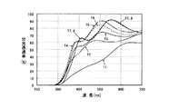
図5に、ArとO2の総流量に対してO2流量を0%から4%まで変化させて成膜した時の半透過膜21の分光透過率データを示す。図5で、波長380nmでの分光透過率は、T1:18.2%、T2:41.8%、T3:53.8%、T4:62.4%、T5:63.2%となり、番号が大きくなるほど、O2流量を高めて成膜した膜である。一方、波長300nmでの透過率は全て5%以下を満足している。この結果から、T3以上でほぼ所望の分光透過率特性が得られるが、これはほぼ0.6%以上のO2流量で作製した膜である。
さらに、その上にCr膜等からなる遮光膜31を形成して、本発明の液晶表示素子製造用の露光マスク用ブランク10を得る。半透過膜21と遮光膜31の膜厚はそれぞれ2500Å、1000Å程度であり、遮光膜31は金属Cr膜の上に酸化Cr膜を積層した2層構成が一般的である。
Hereinafter, the manufacturing method of the blank for exposure masks of this invention is demonstrated.
In the method for manufacturing an exposure mask blank 10 according to claim 4, first, an alloy target of In and Sn is used on a
FIG. 5 shows spectral transmittance data of the
Further, a
上記露光マスク用ブランク10を用いて、請求項5に係る本発明の露光マスクの作製法について説明する。
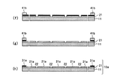
図6(a)〜(e)及び図7(f)〜(h)に本発明の液晶表示素子製造用の露光マスク用ブランクを用いて本発明の露光マスクを作成する製造方法の一例を示す。
まず、透明基板11上に、キャリアガスとしてArガスを用い、O2の割合が総流量に対して0.6%のAr、O2の混合ガス雰囲気にて、InとSnの合金ターゲットを用いた反応性スパッターにて、波長300nmで5%以下、波長380nmでは45%以上の透過率特性を有するITO膜からなる半透過膜21を成膜し、さらにその上にCr及び酸化Cr膜からなる遮光膜31を形成して露光マスク用ブランク10を作製する(図6(a)参照)。
ここで、半透過膜21の膜厚は2000〜3000Å程度、遮光膜31は1000Å前後である。
A method for producing an exposure mask of the present invention according to
FIGS. 6A to 6E and FIGS. 7F to 7H show an example of a manufacturing method for producing the exposure mask of the present invention using the exposure mask blank for manufacturing the liquid crystal display element of the present invention. .
First, use on the
Here, the film thickness of the
次に、電子線ポジ型レジストを用いてスピンナー塗布等により所定厚のレジスト41を形成する(図6(b)参照)。
次に、電子ビーム露光装置にてパターン描画を行い、現像処理して、完全にレジストを除去した開口部42と、露光ドーズ量を調整して一部レジストを残したレジストパターン41aを形成する(図6(c)参照)。
Next, a
Next, pattern drawing is performed by an electron beam exposure apparatus, and development processing is performed to form an
次いで、このレジストパターン41aをマスクにして開口部42の遮光膜31のエッチングを行なう(図6(d)参照)。さらに引き続いて、半透過膜21のエッチングを行なう(図6(e)参照)。
ここで、遮光膜31のエッチャントとしては、[硝酸第2セリウムアンモニウム]+HClO4+H2OからなるCrエッチャントを、半透過膜21のエッチャントとしては、FeCl3+HCl(FeCl3:HCl=1:3)をそれぞれ用いる。
Next, the
Here, as the etchant of the
次いで、全面露光を行ない、レジストパターン41aを遮光膜31界面まで現像により除去し、レジストパターン41bを形成する(図7(f)参照)。
このとき、レジストパターン41a以外のレジストは残すため、オーバー露光にならないように注意する。
次に、レジストパターン41bをマスクにして上記Crエッチャントにて遮光膜31をエッチングにて除去する(図7(g)参照)。
Next, overall exposure is performed, and the resist
At this time, since the resist other than the resist
Next, the
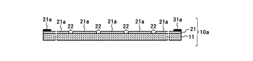
最後に、レジストパターン41bを剥離することにより、波長300nmで5%以下、波長380nmでは45%以上の透過率特性を有する半透過膜によるマスクパターン21a、開口部22及び遮光パターン31aを有する本発明の露光マスク10aを得る(図7(h)参照)。
ここで、露光マスク10aのマスクパターン21a、開口部22及び遮光パターン31aは、開口部22が柱状スペーサー形成用のパターンとして、マスクパターン21aがオーバーコート層形成用のパターンとして、遮光パターン31aがオーバーコート層のパターニング用として作用する。
Finally, the present invention has a
Here, the
以下、請求項6または7に係る本発明の液晶表示装置用カラーフィルタの作製法について述べる。
図8(a)〜(e)及び図9(f)〜(h)は液晶表示装置用カラーフィルタの製造工程の一例を示す部分構成断面図である。
まず、ガラス基板51の裏面に裏ITO52を形成する(図8(a)参照)。
次に、カーボンブラック等の遮光剤を分散した黒色の感光性樹脂層を形成し、パターン露光、現像等の一連のパターニング処理を行って、ガラス基板51上の所定位置にブラックマトリックス53を形成する(図8(b)参照)。
ここで、裏ITO52としては酸化インジウム系の透明導電膜が一般的である。
また、遮光材としては、カーボンブラックの他に酸化チタン、四酸化鉄等の金属酸化物粉、金属硫化物粉、金属粉及び赤、青、緑色等の顔料の混合物等を用いることができる。
Hereinafter, a method for producing a color filter for a liquid crystal display device according to the present invention according to claim 6 or 7 will be described.
FIGS. 8A to 8E and FIGS. 9F to 9H are partial configuration cross-sectional views illustrating an example of a manufacturing process of a color filter for a liquid crystal display device.
First, the
Next, a black photosensitive resin layer in which a light shielding agent such as carbon black is dispersed is formed, and a series of patterning processes such as pattern exposure and development are performed to form a
Here, the
In addition to carbon black, a metal oxide powder such as titanium oxide or iron tetroxide, a metal sulfide powder, a metal powder, and a mixture of pigments such as red, blue, and green can be used as the light shielding material.
次に、赤色の有機顔料をエポキシ系、アクリル系、ポリイミド系、ウレタン系、ポリエステル系及びポリビニル系等の樹脂溶液に分散し、感光性を持たせた着色感光性樹脂溶液をスピンナー等により塗布して、感光性樹脂層を形成し、パターン露光、現像等の一連のパターニング処理を行って、ガラス基板51上の所定位置のブラックマトリックス53間に赤色フィルタ61Rを形成する(図8(c)参照)。
Next, a red organic pigment is dispersed in a resin solution such as epoxy, acrylic, polyimide, urethane, polyester, and polyvinyl, and a photosensitive photosensitive colored resin solution is applied with a spinner or the like. Then, a photosensitive resin layer is formed, and a series of patterning processes such as pattern exposure and development are performed to form a
次に、緑色の有機顔料をエポキシ系、アクリル系、ポリイミド系、ウレタン系、ポリエステル系及びポリビニル系等の樹脂溶液に分散し、感光性を持たせた着色感光性樹脂溶液をスピンナー等により塗布して、感光性樹脂層を形成し、パターン露光、現像等の一連のパターニング処理を行って、ガラス基板51上の所定位置のブラックマトリックス53間に緑色フィルタ62Gを形成する(図8(d)参照)。
Next, a green organic pigment is dispersed in an epoxy, acrylic, polyimide, urethane, polyester, and polyvinyl resin solution, and a photosensitive photosensitive colored resin solution is applied with a spinner or the like. Then, a photosensitive resin layer is formed and a series of patterning processes such as pattern exposure and development are performed to form a
次に、青色の有機顔料をエポキシ系、アクリル系、ポリイミド系、ウレタン系、ポリエステル系及びポリビニル系等の樹脂溶液に分散し、感光性を持たせた着色感光性樹脂溶液をスピンナー等により塗布して、感光性樹脂層を形成し、パターン露光、現像等の一連のパターニング処理を行って、ガラス基板51上の所定位置のブラックマトリックス53間に青色フィルタ63Bを形成する(図8(e)参照)。
上記赤色、緑色、青色の有機顔料としてはフタロシアニン系、アジレーキ系、縮合アゾ系、キナクリドンアントラキノン系、ペリレン系及びペリノン系等が使用される。
Next, a blue organic pigment is dispersed in an epoxy-based, acrylic-based, polyimide-based, urethane-based, polyester-based or polyvinyl-based resin solution, and a photosensitive photosensitive colored resin solution is applied with a spinner or the like. Then, a photosensitive resin layer is formed, and a series of patterning processes such as pattern exposure and development are performed to form a
As the red, green and blue organic pigments, phthalocyanine, azirake, condensed azo, quinacridone anthraquinone, perylene and perinone are used.
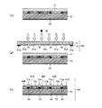
次に、ネガ型の感光性樹脂を用いて柱状スペーサー及びオーバーコート層を形成するための所定厚の感光性樹脂層71を形成する(図9(f)参照)。
感光性樹脂層71の膜厚は、柱状スペーサーの高さによって設定される。
Next, a
The film thickness of the
ここで、ネガ型の感光性樹脂としては、エポキシ系、アクリル系ノボラック系の感光性樹脂が使用できる。 Here, as the negative photosensitive resin, an epoxy-based or acrylic novolak-based photosensitive resin can be used.
次に、マスクパターン21a、開口部22及び遮光パターン31aを有する本発明の露光マスク10aを用いて感光性樹脂層71を露光する(図9(g)参照)。
感光性樹脂層71の膜厚は、柱状スペーサーの高さによって設定される。
この露光処理は感光性樹脂層71に柱状スペーサー及びオーバーコート層のパターン潜像を形成するためのものである。
また、遮光パターン31aは、液晶表示装置用カラーフィルタ周辺部のオーバーコート層を除去するためのものである。
Next, the
The film thickness of the
This exposure process is for forming a columnar spacer and an overcoat layer pattern latent image on the
The
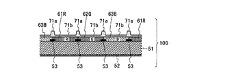
次に、所定の現像液で感光性樹脂層71を現像処理し、柱状スペーサー71a及びオーバーコート層71bを形成し、本発明の液晶表示装置用カラーフィルタ100を得る(図9(h)参照)。
このように、本発明の露光マスク10aを用いることにより、1回の露光で高さの異なる柱状スペーサー71a及びオーバーコート層71bを形成することができ、液晶表示装置用カラーフィルタの製造工程の簡略化及び液晶表示装置用カラーフィルタの製造コストの低減につなげることができる。
ここで、柱状スペーサー71aはブラックマトリックス53上に形成され、高さ5μm前後の柱状が一般的である。オーバーコート層71bは赤色、緑色及び青色カラーフィルタ上に形成され、高さ1.5μm前後の膜厚が一般的である。
また、液晶表示装置用カラーフィルタ100は横電界方式の液晶表示装置に組み込まれ、視野角の広いカラー液晶ディスプレイとして展開されている。
Next, the
Thus, by using the
Here, the
The
まず、ガラス基板11上に、キャリアガスとしてArガスを用いたガス圧0.25Pa
のAr、O2の混合ガス雰囲気にて、O2の割合が総流量に対して0.6%のAr、O2の混合ガス雰囲気にて、InとSnの合金ターゲットを用いた反応性スパッターにて膜厚2500Åの波長300nmで5%以下、波長380nmでは45%以上の透過率特性を有するITO膜からなる半透過膜21を形成した。
さらに、その上にCr及び酸化Cr膜からなる膜厚1000Åの遮光膜31をスパッターにて形成して露光マスク用ブランク10を作製した(図1参照)
First, a gas pressure of 0.25 Pa using Ar gas as a carrier gas on the
Of Ar, a mixed gas atmosphere of O 2, 0.6% of Ar ratio of O 2 is the total flow rate, a mixed gas atmosphere of O 2, reactive sputtering using an alloy target of In and Sn A
Further, a light-shielding
まず、露光マスク用ブランク10上に、電子線ポジ型レジストを用いてスピンナー塗布等により所定厚のレジスト41を形成した(図6(a)及び(b)参照)。
次に、電子ビーム露光装置にてパターン描画を行い、現像処理して、完全にレジストを除去した開口部42と、露光ドーズ量を調整して一部レジストを残したレジストパターン41aを形成した(図6(c)参照)
次に、レジストパターン41aをマスクにして開口部42の遮光膜31を[硝酸第2セリウムアンモニウム]+HClO4+H2OからなるCrエッチャントを用いてエッチングした(図6(d)参照)。
さらに、FeCl3+HCl(FeCl3:HCl=1:3)からなるエッチャントを用いて、半透過膜21のエッチングを行なった(図6(e)参照)。
First, a resist 41 having a predetermined thickness was formed on the exposure mask blank 10 by spinner coating or the like using an electron beam positive resist (see FIGS. 6A and 6B).
Next, pattern drawing was performed with an electron beam exposure apparatus, and development processing was performed to form an
Next, using the resist
Further, the
次に、全面露光を行ない、現像にてレジストパターン41aを除去し、レジストパターン41bを形成した(図7(f)参照)。
次に、レジストパターン41bをマスクにして[硝酸第2セリウムアンモニウム]+HClO4+H2OからなるCrエッチャントにて遮光膜31をエッチングにて除去した(図7(g)参照)。
Next, overall exposure was performed, the resist
Next, using the resist
最後に、レジストパターン41bを剥離することにより、マスクパターン21a、開口部22及び遮光パターン31aを有する本発明の露光マスク10aを得た(図2及び図7(h)参照)。
Finally, the resist
まず、0.7mm厚の無アルカリガラス(OA−2:日本電気硝子(株)製)からなるガラス基板51の裏面に裏ITO52を形成した(図8(a)参照)。
次に、ガラス基板51上にアクリル系樹脂にカーボンブラックを分散した黒色の感光性樹脂溶液をスピンナーで塗布し、黒色感光性樹脂層を形成し、パターン露光、現像等の一連のパターニング処理を行って、幅14μm、高さ1.3μmのブラックマトリクス53を形成した(図8(b)参照)。
First, a
Next, a black photosensitive resin solution in which carbon black is dispersed in an acrylic resin is applied on the
次に、アクリル系樹脂にジアントラキノン系顔料を分散した感光性樹脂溶液をスピンナーを用いて塗布し、赤色感光性樹脂層を形成し、所定の露光マスクを使ってパターン露光、現像等の一連のパターニング処理及び加熱硬化処理を行って、幅80μm、膜厚1.3μmの赤色カラーフィルタ61Rを形成した(図8(c)参照)。
Next, a photosensitive resin solution in which a dianthraquinone pigment is dispersed in an acrylic resin is applied using a spinner, a red photosensitive resin layer is formed, and a series of pattern exposure, development, etc. is performed using a predetermined exposure mask. A patterning process and a heat curing process were performed to form a
次に、アクリル系樹脂にフタロシアニングリーン系顔料を分散した感光性樹脂溶液をスピンナーで塗布し、緑色感光性樹脂層を形成し、所定の露光マスクを使ってパターン露光、現像等の一連のパターニング処理及び加熱硬化処理を行って、幅80μm、膜厚1.3μmの緑色カラーフィルタ62Gを形成した(図8(d)参照)。
Next, a photosensitive resin solution in which phthalocyanine green pigment is dispersed in an acrylic resin is applied with a spinner to form a green photosensitive resin layer, and a series of patterning processes such as pattern exposure and development using a predetermined exposure mask Then, a heat curing treatment was performed to form a
次に、アクリル系樹脂にフタロシアニンブルー系顔料を分散した感光性樹脂溶液をスピンナーで塗布し、青色感光性樹脂層を形成し、所定の露光マスクを使ってパターン露光、現像等の一連のパターニング処理及び加熱硬化処理を行って、幅80μm、膜厚1.3μ
mの青色カラーフィルタ63Bを形成した(図8(e)参照)。
Next, a photosensitive resin solution in which a phthalocyanine blue pigment is dispersed in an acrylic resin is applied with a spinner to form a blue photosensitive resin layer, and a series of patterning processes such as pattern exposure and development using a predetermined exposure mask. And heat curing treatment,
A
次に、アクリル系樹脂を主成分とした感光性樹脂溶液をスピンナーで塗布し、カラーフィルタ上に5μm厚の感光性樹脂層71を形成した(図9(f)参照)。
Next, a photosensitive resin solution containing acrylic resin as a main component was applied with a spinner to form a
次に、マスクパターン21a、開口部22及び遮光パターン31aを有する本発明の露光マスク10aを用いて感光性樹脂層71を露光した(図9(g)参照)。
Next, the
次に、アルカリ現像液で感光性樹脂層71を現像処理し、高さ5μm、幅14μmの柱状スペーサー71a及び1.0μm厚のオーバーコート層71bを形成し、本発明の液晶表示装置用カラーフィルタ100を得た(図9(h)参照)。
Next, the
上記したように、本発明の露光マスク10aを用いることにより、液晶表示装置用カラーフィルタ上に1回の露光で高さの異なる柱状スペーサー71a及びオーバーコート層71bを形成することができ、液晶表示装置用カラーフィルタの製造工程の簡略化及び液晶表示装置用カラーフィルタの製造コストの低減につなげることができる。
As described above, by using the
10……露光マスク用ブランク
10a、10b……露光マスク
11、51……ガラス基板
21……半透過膜
21a……マスクパターン
22……開口部
31……遮光膜
31a……遮光パターン
41……レジスト
41a、41b……レジストパターン
42……開口部
52……裏ITO
53……ブラックマトリクス
61R……赤色フィルタ
62G……緑色フィルタ
63B……青色フィルタ
71……感光性樹脂層
71a……柱状スペーサー
71b……オーバーコート層
72……ネガレジスト
72a、72b……レジストパターン
73……オーバーコート層
74……柱状スペーサー
P1、P2……マスクパターン
DESCRIPTION OF
53 ……
Claims (4)
この露光マスク用ブランクが、ガラス基板上に紫外線透過率制御機能を有する半透過膜と紫外線遮蔽効果を有する遮光膜とが形成されているものであり、
前記半透過膜が、キャリアガスと酸素ガスを用いた反応性スパッタリングにより成膜され、前記酸素ガス流量の割合が総流量に対して0.6%以上になっていることを特徴とする露光マスク用ブランクの製造方法。 A method for producing a blank for an exposure mask for collectively forming columnar spacers and an overcoat layer of a color filter for a liquid crystal display device,
In this exposure mask blank, a semi-transmissive film having an ultraviolet transmittance control function and a light shielding film having an ultraviolet shielding effect are formed on a glass substrate,
The semi-transmissive film is formed by reactive sputtering using a carrier gas and an oxygen gas, and the ratio of the oxygen gas flow rate is 0.6% or more with respect to the total flow rate. Of manufacturing blanks.
Priority Applications (1)
| Application Number | Priority Date | Filing Date | Title |
|---|---|---|---|
| JP2004375913A JP4635604B2 (en) | 2004-12-27 | 2004-12-27 | Method for manufacturing exposure mask blank, exposure mask, method for manufacturing color filter for liquid crystal display device, and color filter for liquid crystal display device |
Applications Claiming Priority (1)
| Application Number | Priority Date | Filing Date | Title |
|---|---|---|---|
| JP2004375913A JP4635604B2 (en) | 2004-12-27 | 2004-12-27 | Method for manufacturing exposure mask blank, exposure mask, method for manufacturing color filter for liquid crystal display device, and color filter for liquid crystal display device |
Publications (2)
| Publication Number | Publication Date |
|---|---|
| JP2006184399A JP2006184399A (en) | 2006-07-13 |
| JP4635604B2 true JP4635604B2 (en) | 2011-02-23 |
Family
ID=36737585
Family Applications (1)
| Application Number | Title | Priority Date | Filing Date |
|---|---|---|---|
| JP2004375913A Expired - Fee Related JP4635604B2 (en) | 2004-12-27 | 2004-12-27 | Method for manufacturing exposure mask blank, exposure mask, method for manufacturing color filter for liquid crystal display device, and color filter for liquid crystal display device |
Country Status (1)
| Country | Link |
|---|---|
| JP (1) | JP4635604B2 (en) |
Families Citing this family (8)
| Publication number | Priority date | Publication date | Assignee | Title |
|---|---|---|---|---|
| JP4978128B2 (en) * | 2006-09-22 | 2012-07-18 | 大日本印刷株式会社 | Photocurable resin composition |
| JP5046005B2 (en) * | 2007-03-29 | 2012-10-10 | 大日本印刷株式会社 | Method for manufacturing element for liquid crystal display device |
| JP5092576B2 (en) * | 2007-06-25 | 2012-12-05 | 凸版印刷株式会社 | Exposure mask blank |
| JP5245303B2 (en) * | 2007-06-29 | 2013-07-24 | 凸版印刷株式会社 | Method for manufacturing color filter substrate and method for manufacturing liquid crystal display device |
| JP5381051B2 (en) * | 2008-12-01 | 2014-01-08 | 大日本印刷株式会社 | Multispectral mask and color filter manufacturing method |
| JP2010266579A (en) * | 2009-05-13 | 2010-11-25 | Toppan Printing Co Ltd | Color filter substrate |
| KR101032705B1 (en) | 2010-11-16 | 2011-06-02 | 주식회사 에스앤에스텍 | Mask blanks, methods of making mask blanks and photomasks |
| CN114527591B (en) * | 2022-03-30 | 2023-08-01 | Tcl华星光电技术有限公司 | Preparation method of liquid crystal display panel and liquid crystal display panel |
Family Cites Families (6)
| Publication number | Priority date | Publication date | Assignee | Title |
|---|---|---|---|---|
| JPS6255653A (en) * | 1985-09-03 | 1987-03-11 | Matsushita Electric Ind Co Ltd | Production of photomask |
| JP3498020B2 (en) * | 1999-09-29 | 2004-02-16 | Nec液晶テクノロジー株式会社 | Active matrix substrate and manufacturing method thereof |
| JP2003029393A (en) * | 2001-07-12 | 2003-01-29 | Matsushita Electric Ind Co Ltd | Mask, pattern forming method and lithography method using the same |
| JP3912663B2 (en) * | 2002-02-26 | 2007-05-09 | 富士フイルム株式会社 | Color filter pixel formation method, liquid crystal display color filter, liquid crystal display spacer and alignment control protrusion formation method, liquid crystal display spacer and alignment control protrusion |
| JP4385690B2 (en) * | 2003-09-09 | 2009-12-16 | 凸版印刷株式会社 | Exposure mask for manufacturing liquid crystal display element and method for manufacturing the same |
| JP4617821B2 (en) * | 2004-10-21 | 2011-01-26 | 凸版印刷株式会社 | LIQUID CRYSTAL DISPLAY DEVICE SUBSTRATE, LIQUID CRYSTAL DISPLAY DEVICE SUBSTRATE MANUFACTURING METHOD, AND PHOTO MASK USED FOR THE METHOD |
-
2004
- 2004-12-27 JP JP2004375913A patent/JP4635604B2/en not_active Expired - Fee Related
Also Published As
| Publication number | Publication date |
|---|---|
| JP2006184399A (en) | 2006-07-13 |
Similar Documents
| Publication | Publication Date | Title |
|---|---|---|
| US7826010B2 (en) | Color filter substrate and method of manufacturing the same | |
| JP5200439B2 (en) | Manufacturing method of color filter | |
| JP5228390B2 (en) | Gradation mask | |
| US9360700B2 (en) | Half-transmitting and half-reflecting color film substrate, manufacture method thereof and liquid crystal display device | |
| JP4385690B2 (en) | Exposure mask for manufacturing liquid crystal display element and method for manufacturing the same | |
| JP5673718B2 (en) | Gradation mask | |
| JP4635604B2 (en) | Method for manufacturing exposure mask blank, exposure mask, method for manufacturing color filter for liquid crystal display device, and color filter for liquid crystal display device | |
| JP2005316365A (en) | Liquid crystal display device provided with patterned spacer and manufacturing method thereof | |
| JP5094010B2 (en) | Color filter substrate for liquid crystal display device and manufacturing method thereof | |
| JP4848932B2 (en) | Tone mask for proximity exposure | |
| JP4915093B2 (en) | Manufacturing method of color filter | |
| CN100405167C (en) | Color filter substrate and manufacturing method thereof | |
| JP5382194B2 (en) | Manufacturing method of color filter | |
| JP4858025B2 (en) | Gradation mask | |
| JP4617821B2 (en) | LIQUID CRYSTAL DISPLAY DEVICE SUBSTRATE, LIQUID CRYSTAL DISPLAY DEVICE SUBSTRATE MANUFACTURING METHOD, AND PHOTO MASK USED FOR THE METHOD | |
| JP5298424B2 (en) | Manufacturing method of color filter | |
| JP5028768B2 (en) | Color filter manufacturing method and liquid crystal display device | |
| JP2010175597A (en) | Photomask, method for manufacturing color filter, color filter, and liquid crystal display device | |
| JP5169072B2 (en) | Manufacturing method of color filter for liquid crystal display device | |
| JP4775113B2 (en) | Color filter manufacturing method, color filter, and liquid crystal display device | |
| JP4706334B2 (en) | Photomask with steps and method for manufacturing color filter substrate | |
| JP5516523B2 (en) | Manufacturing method of color filter | |
| WO2011055593A1 (en) | Spacer forming method, method of manufacturing display panel substrate, spacer, and display panel substrate | |
| JPH01277202A (en) | Production of color filter with transparent electrode | |
| JP5151344B2 (en) | Manufacturing method of color filter |
Legal Events
| Date | Code | Title | Description |
|---|---|---|---|
| A621 | Written request for application examination |
Free format text: JAPANESE INTERMEDIATE CODE: A621 Effective date: 20071122 |
|
| A977 | Report on retrieval |
Free format text: JAPANESE INTERMEDIATE CODE: A971007 Effective date: 20100729 |
|
| A131 | Notification of reasons for refusal |
Free format text: JAPANESE INTERMEDIATE CODE: A131 Effective date: 20100804 |
|
| A521 | Request for written amendment filed |
Free format text: JAPANESE INTERMEDIATE CODE: A523 Effective date: 20100922 |
|
| TRDD | Decision of grant or rejection written | ||
| A01 | Written decision to grant a patent or to grant a registration (utility model) |
Free format text: JAPANESE INTERMEDIATE CODE: A01 Effective date: 20101026 |
|
| A01 | Written decision to grant a patent or to grant a registration (utility model) |
Free format text: JAPANESE INTERMEDIATE CODE: A01 |
|
| A61 | First payment of annual fees (during grant procedure) |
Free format text: JAPANESE INTERMEDIATE CODE: A61 Effective date: 20101108 |
|
| FPAY | Renewal fee payment (event date is renewal date of database) |
Free format text: PAYMENT UNTIL: 20131203 Year of fee payment: 3 |
|
| R150 | Certificate of patent or registration of utility model |
Ref document number: 4635604 Country of ref document: JP Free format text: JAPANESE INTERMEDIATE CODE: R150 |
|
| R250 | Receipt of annual fees |
Free format text: JAPANESE INTERMEDIATE CODE: R250 |
|
| LAPS | Cancellation because of no payment of annual fees |