JP4635381B2 - Electronic control unit - Google Patents
Electronic control unit Download PDFInfo
- Publication number
- JP4635381B2 JP4635381B2 JP2001173051A JP2001173051A JP4635381B2 JP 4635381 B2 JP4635381 B2 JP 4635381B2 JP 2001173051 A JP2001173051 A JP 2001173051A JP 2001173051 A JP2001173051 A JP 2001173051A JP 4635381 B2 JP4635381 B2 JP 4635381B2
- Authority
- JP
- Japan
- Prior art keywords
- substrate
- electronic control
- body portion
- case member
- slit
- Prior art date
- Legal status (The legal status is an assumption and is not a legal conclusion. Google has not performed a legal analysis and makes no representation as to the accuracy of the status listed.)
- Expired - Fee Related
Links
Images


Landscapes
- Regulating Braking Force (AREA)
- Connector Housings Or Holding Contact Members (AREA)
- Mounting Of Printed Circuit Boards And The Like (AREA)
Description
【0001】
【発明の属する技術分野】
本発明は、電子制御装置に関し、より詳細にはABS(アンチロックブレーキシステム)等の圧力制御装置を駆動、制御する電子制御装置に関する。
【0002】
【従来の技術】
この種の圧力制御装置としては、図6乃至図9に示されたものがある。図7は、図6のC−C断面図であり、図8は、後述する熱変形を示す断面図である。また、図9は、後述する基板保持部の詳細断面図である。
【0003】
この装置は、表面に電子部品(図示省略)が配置されるとともに装着穴114、115、116及び117を有する基板111と、方形を呈する本体部122と本体部の一辺122aにおいて本体部122に対してオーバハングして一体的に形成されて方形を呈するコネクタ部123とを有するケース部材121と、ケース部材121上に形成されるとともに装着穴に嵌入して基板111を固定する基板保持部124、125、126及び127を備えた電子制御装置105である。
【0004】
基板保持部124、125、126及び127は、それぞれ円筒部124b、125b、126b及び127bと円筒部の直径より所定寸法大きい底部を有する円錐台状の先端部124c、125c、126c及び127cとからなる突起124a、125a、126a及び127aと、基板111の重量を支える支持部124d、125d、126d及び127dとからなる。また、突起124a、125a、126a及び127aは、それぞれ基板111に直角に形成されたスリット124e、125e、126e及び127eが設けられているため、装着穴112、113、114及び115に嵌入される際にばね作用を生じる。このため、基板111がワンタッチで簡単に装着されるとともに他の固定手段を用いることなく確実に基板111が固定されるいわゆるスナップフィットが実現され、基板111のケース部材121への組付け工数が削減される。
【0005】
【発明が解決しようとする課題】
この種の従来装置は、車両のエンジンルーム内に搭載されるため、エンジンの発生熱によるケース部材の変形(図8に示す)が生じ、特に本体部からオーバハングしているコネクタ部の反りが大きい。また、本体部に比べて小さい方形のコネクタ部と方形の本体部とを一体的に形成してあるため一様に変形せず、反り変極線(図6の線D。反りの基点となる部位)は、本体部とコネクタ部とが一体化されている方形の一辺(図6の線122a)に対して角度θを持つことになる。このとき、基板保持部によってケース部材に固定されている基板もケース部材の変形にならって変形する。
【0006】
ところで、スリットを有する突起は、スリットと直角方向には変形しやすく、スリットと平行方向には変形し難いものであるが、従来装置においては、スリットが本体部とコネクタ部とが一体化されている方形の一辺(図6の線122a)と平行に形成されていて、スリットと反り変極線とが平行でないため、コネクタ部の反りに対して突起の変形が起き難い。このため、基板は、図8に示すように『くの字』状に折り曲げられ、反り変極線近傍のハンダが割れて導通不良や電子部品の脱落の虞があった。
【0007】
本発明は、以上の事情を背景に為されたものであり、ケース部材に熱変形が生じた場合でも基板に曲げ力が加わることがなく、基板上のハンダに割れが生じることのない、信頼性の高い電子制御装置を提供することをその技術的課題とするものである。
【0008】
【課題を解決するための手段】
上記技術的課題を解決するために、請求項1に記載のように、表面に電子部品が配置されるとともに複数の装着穴を有する基板と、前記基板を収容し方形を呈する本体部と前記本体部の一辺において前記本体部に対してオーバハングして一体的に形成されて方形を呈するコネクタ部とを有するケース部材と、前記ケース部材上に形成されるとともに前記装着穴に嵌入して前記基板を固定する複数の基板保持部とを備えた電子制御装置において、前記基板保持部は、前記基板に対して直角に形成されたスリットを有する突起を備え、前記基板に対して平行である前記スリットの長手方向軸は、前記基板の平面視状態において、前記ケース部材の熱変形における反りの基点となる反り変極線と平行であることを特徴とする電子制御装置を構成した。
【0009】
請求項1にかかる発明によれば、スリットをその長手方向軸が基板の平面視状態においてケース部材の反り変極線と平行となるように形成したため、コネクタ部の反りに応じて突起が容易に傾斜することが可能となる。このため、基板が突起によって拘束されて『くの字』状に折れ曲がることがないため、ハンダの割れが発生せず、信頼性の高い電子制御装置を提供することが可能となる。
【0010】
【発明の実施の形態】
以下、本発明にかかる電子制御装置の実施形態について、図面に基いて説明する。
【0011】
図1乃至図5に、本発明にかかる第1実施形態を示す。
【0012】
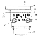
図1において、電子制御装置5は、下面にモータ10が取付けられるとともに内部にはモータ10の駆動力を受けて作動する液圧ポンプ、圧力制御弁、液圧通路及び複数の電磁弁(いずれも図示せず)が設けられたブレーキ液圧ユニット11の上部に一体的に取付けられている。なお、電子制御装置5及びブレーキ液圧ユニット11は、通常エンジンルーム内に搭載される。
【0013】
また、ブレーキ液圧ユニット11の上面には、コイル31がカシメ等によって固定されるとともに、コイル31を覆うように下部樹脂製ケース21(ケース部材)がねじによって固定されている。なお、圧力制御弁とコイル31とによって、電磁弁が構成される。
【0014】
下部樹脂製ケース21と上部樹脂製ケース20とは、溶着等によって強固に接続されるとともに、下部樹脂製ケース21および上部樹脂製ケース20の内部は、気密的、液密的に大気から遮断される。
【0015】
図2は、上部樹脂製ケース20と基板11とを取り除いた電子制御装置5の平面図である。図2において、下部樹脂製ケース21は、方形の本体部22と本体部22の一辺22aにおいて本体部22に対してオーバハングして一体的に形成されたコネクタ部23とからなる。
【0016】
下部樹脂製ケース21には、基板を保持するための基板保持部24、25及び26が下部樹脂製ケース21に一体的に設けられている。
【0017】
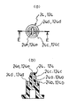
基板保持部24及び25の断面形状は、図9に示した従来の電子制御装置のケース部材に設けられた基板保持部と同じ形状であり、それぞれ円筒部24b、25bと円筒部24b、25bの直径より所定寸法大きい底部を有する円錐台状の先端部24c、25cとからなる突起24a、25aと、基板11の重量を支える支持部24d、25dとからなる。
【0018】
突起24a、25aは、それぞれ基板11に直角に形成されたスリット24e、25eが設けられているため、装着穴14、15に嵌入される際にばね作用を生じる。このため、基板11がワンタッチで簡単に装着されるとともに他の固定手段を用いることなく確実に基板11が固定されるいわゆるスナップフィットが実現され、基板11の下部樹脂製ケース21への組付け工数が削減される。
【0019】
下部樹脂製ケース21には、基板を保持するための基板保持部26が下部樹脂製ケース21と一体的に設けられている。
【0020】
図5に示すように、基板保持部26は、前述した基板保持部24、25と断面形状を異にする。すなわち、基板保持部26は、基板11に直角に形成されたスリット26eを有する円筒状の突起26aと、基板11の重量を支える支持部26dとからなり、円錐台状の先端部を有さない。したがって、基板保持部26は、基板保持部24、25と異なり、スナップフィット機能を有さず、所定の拡張力を持って装着穴16に嵌入されるのみである。
【0021】
なお、突起24a、25a及び26aは、それぞれスリット24e、25e及び26eの長手方向軸に対して直角方向には変形しやすく、スリットと平行方向には変形し難い。
【0022】
また、突起24a、25a及び26aにそれぞれ形成されたスリット24e、25e及び26eの長手方向軸は、方形の本体部22の一辺22aに対して平行でなく、所定の角度θだけ傾けて設けられている。
【0023】
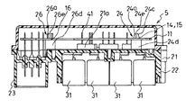
電子制御装置5は、エンジンルーム内に搭載され、エンジンの発生熱によって下部樹脂製ケース21が変形する。特に本体部22からオーバハングしているコネクタ部23の反りが大きく、本体部22に比べて小さい方形のコネクタ部23と方形の本体部22とを一体的に形成してあるため一様に変形しない。このため、反り変極線(図2の線B。反りの基点となる部位)は、本体部22とコネクタ部23とが一体化されている方形の一辺(図2の線22a)に対して角度θを持つことになる。
【0024】
本実施形態においては、方形の一辺に対する反り変極線の角度と方形の一辺に対するスリット24e、25e及び26eの長手方向軸の角度とを同じθとしている。したがって、コネクタ部23に熱変形による反りが発生して基板11を屈曲させようとしても、反り変極線と同じ角度だけ長手方向軸が傾斜しているスリット24e、25e、26eを有する突起24a、25a、26aは、容易に傾くことが可能であるとともに、装着穴16においてスナップフィットしていない基板11は、突起26aに対して上下方向(図3、図4における上下方向)にスライド可能である。このため、基板11は、曲げ力が加わることなくコネクタ部23の反りに追従することが可能となる(図4)。
【0025】
すなわち、本実施形態においては、熱変形によってコネクタ部23に反りが発生しても、基板11が『くの字』に屈曲することがなく、基板上のハンダに割れが生じることがない。
【0026】
なお、上記実施形態において、基板保持部26は、基板11に直角に形成されたスリット26eを有する円筒状の突起26aと、基板11の重量を支える支持部26dとからなり、円錐台状の先端部を有さず、スナップフィット機能を有さない。
【0027】
しかしながら、この形態に限定されるものではなく、基板保持部26の突起26aが、図9に示される円錐台状の先端部を有していてもよい。すなわち、反り変極線と同じ角度だけ長手方向軸が傾斜しているスリット26eを有する突起26aは、容易に傾くことが可能であるため、基板11は、曲げ力が加わることなくコネクタ部23の反りに追従することが可能である。
【0028】
【発明の効果】
以上に説明したように、本発明によれば、ケース部材に熱変形が生じた場合でも基板に曲げ力が加わることがなく、基板上のハンダに割れが生じない信頼性の高い電子制御装置を提供することが可能となる。
【図面の簡単な説明】
【図1】本発明にかかる電子制御装置がブレーキ液圧ユニットに装着された状態を示す正面図である。
【図2】本発明の実施形態にかかる電子制御装置の平面図である。
【図3】図2におけるA−A断面図である。
【図4】コネクタ部の熱変形を示す断面図である。
【図5】本発明の実施形態にかかる電子制御装置の基板保持部を示す平面図及び断面図である。
【図6】従来の電子制御装置の平面図である。
【図7】図6におけるC−C断面図である。
【図8】従来の電子制御装置のコネクタ部の熱変形を示す断面図である。
【図9】従来の電子制御装置の基板保持部を示す平面図及び断面図である。
【符号の説明】
5 電子制御装置
11 基板
14、15、16 装着穴
21 下部樹脂製ケース(ケース部材)
22 本体部
22a 一辺
23 コネクタ部
24、25、26 基板保持部
24a、25a、26a 突起
24e、25e、26e スリット[0001]
BACKGROUND OF THE INVENTION
The present invention relates to an electronic control device, and more particularly to an electronic control device that drives and controls a pressure control device such as an ABS (anti-lock brake system).
[0002]
[Prior art]
An example of this type of pressure control device is shown in FIGS. 7 is a cross-sectional view taken along the line CC of FIG. 6, and FIG. 8 is a cross-sectional view illustrating thermal deformation described later. FIG. 9 is a detailed cross-sectional view of a substrate holding portion to be described later.
[0003]
The device includes a
[0004]
The
[0005]
[Problems to be solved by the invention]
Since this type of conventional device is mounted in the engine room of a vehicle, the case member is deformed by the heat generated by the engine (shown in FIG. 8), and particularly the warpage of the connector portion overhanging from the main body portion is large. . Moreover, not uniformly deformed because that is integrally formed with the main body portion of the connector portion in the form the lesser the square than the body portion, the warp inflection line (base line D. warp of 6 ) Has an angle θ with respect to one side of the square (line 122a in FIG. 6) in which the main body and the connector are integrated. At this time, the substrate fixed to the case member by the substrate holding portion is also deformed following the deformation of the case member.
[0006]
By the way, a protrusion having a slit is easily deformed in a direction perpendicular to the slit and difficult to deform in a direction parallel to the slit. However, in the conventional apparatus, the slit is integrated with the main body portion and the connector portion. 6 is formed in parallel with one side of the square (line 122a in FIG. 6), and the slit is not parallel to the warpage changing line, so that deformation of the protrusion hardly occurs due to warpage of the connector portion. For this reason, as shown in FIG. 8, the board is bent in a “K” shape, and the solder near the warping pole is broken, and there is a risk of poor conduction and dropout of electronic components.
[0007]
The present invention has been made in the background of the above circumstances, and even when the case member is thermally deformed, no bending force is applied to the substrate, and the solder on the substrate is not cracked. It is an object of the present invention to provide a highly functional electronic control device.
[0008]
[Means for Solving the Problems]
In order to solve the above technical problem, as described in claim 1, a substrate having a plurality of mounting holes with the electronic components are disposed on the surface, a main body which develops a square accommodating the substrate the It said fitted into the mounting hole and the case member having a connector portion that Teisu the square are integrally formed, while being formed on said case member to overhang relative to the body portion at one side of the body portion In the electronic control device including a plurality of substrate holding units for fixing the substrate, the substrate holding unit includes a protrusion having a slit formed at a right angle to the substrate, and is parallel to the substrate The longitudinal axis of the slit is parallel to a warp inflection line that becomes a base point of warpage in thermal deformation of the case member in a plan view of the substrate.
[0009]
According to the first aspect of the present invention, since the slit is formed so that the longitudinal axis thereof is parallel to the warp inflection line of the case member in the plan view of the substrate, the protrusion can be easily formed according to the warp of the connector portion. It is possible to incline. For this reason, since the substrate is not restrained by the protrusion and bent into a “<” shape, solder cracks do not occur, and a highly reliable electronic control device can be provided.
[0010]
DETAILED DESCRIPTION OF THE INVENTION
Embodiments of an electronic control device according to the present invention will be described below with reference to the drawings.
[0011]
1 to 5 show a first embodiment according to the present invention.
[0012]
In FIG. 1, an
[0013]
A
[0014]
The
[0015]
FIG. 2 is a plan view of the
[0016]
The
[0017]
The cross-sectional shapes of the
[0018]
Since the protrusions 24a and 25a are provided with
[0019]
The
[0020]
As shown in FIG. 5, the
[0021]
The protrusions 24a, 25a, and 26a are easily deformed in a direction perpendicular to the longitudinal axis of the
[0022]
Further, the longitudinal axes of the projections 24a, 25a and 26a in the
[0023]
The
[0024]
In the present embodiment, the angle of the warp inflection line with respect to one side of the square and the angle of the longitudinal axis of the
[0025]
That is, in the present embodiment, even if the
[0026]
In the above embodiment, the
[0027]
However, it is not limited to this form, and the protrusion 26a of the
[0028]
【The invention's effect】
As described above, according to the present invention, there is provided a highly reliable electronic control device in which bending force is not applied to the substrate even when thermal deformation occurs in the case member, and cracks do not occur in the solder on the substrate. It becomes possible to provide.
[Brief description of the drawings]
FIG. 1 is a front view showing a state in which an electronic control device according to the present invention is mounted on a brake hydraulic pressure unit.
FIG. 2 is a plan view of the electronic control device according to the embodiment of the present invention.
FIG. 3 is a cross - sectional view taken along the line AA in FIG.
FIG. 4 is a cross-sectional view showing thermal deformation of a connector portion.
5A and 5B are a plan view and a cross-sectional view showing a substrate holding part of the electronic control device according to the embodiment of the present invention.
FIG. 6 is a plan view of a conventional electronic control device.
7 is a cross-sectional view taken along the line CC in FIG.
FIG. 8 is a cross-sectional view showing thermal deformation of a connector portion of a conventional electronic control device.
9A and 9B are a plan view and a cross-sectional view showing a substrate holding part of a conventional electronic control device.
[Explanation of symbols]
5
22 Main body 22a One
Claims (1)
Priority Applications (1)
| Application Number | Priority Date | Filing Date | Title |
|---|---|---|---|
| JP2001173051A JP4635381B2 (en) | 2001-06-07 | 2001-06-07 | Electronic control unit |
Applications Claiming Priority (1)
| Application Number | Priority Date | Filing Date | Title |
|---|---|---|---|
| JP2001173051A JP4635381B2 (en) | 2001-06-07 | 2001-06-07 | Electronic control unit |
Publications (2)
| Publication Number | Publication Date |
|---|---|
| JP2002368452A JP2002368452A (en) | 2002-12-20 |
| JP4635381B2 true JP4635381B2 (en) | 2011-02-23 |
Family
ID=19014575
Family Applications (1)
| Application Number | Title | Priority Date | Filing Date |
|---|---|---|---|
| JP2001173051A Expired - Fee Related JP4635381B2 (en) | 2001-06-07 | 2001-06-07 | Electronic control unit |
Country Status (1)
| Country | Link |
|---|---|
| JP (1) | JP4635381B2 (en) |
Families Citing this family (11)
| Publication number | Priority date | Publication date | Assignee | Title |
|---|---|---|---|---|
| JP4956931B2 (en) * | 2005-08-04 | 2012-06-20 | パナソニック株式会社 | Capacitor unit |
| JP2007234649A (en) * | 2006-02-27 | 2007-09-13 | Toshiba Corp | Printed wiring board structure and electronic device |
| DE102007055728A1 (en) | 2006-12-15 | 2008-06-19 | Advics Co., Ltd., Kariya | Fluid pressure control device |
| JP2008195373A (en) * | 2006-12-15 | 2008-08-28 | Advics:Kk | Hydraulic control device |
| US7599189B2 (en) | 2007-01-09 | 2009-10-06 | Advics Co., Ltd. | Board-housing case and fluid pressure control device including thereof |
| JP2009241702A (en) * | 2008-03-31 | 2009-10-22 | Advics Co Ltd | Brake fluid pressure control device |
| JP5342817B2 (en) * | 2008-06-26 | 2013-11-13 | 矢崎総業株式会社 | Mold device and module for electrical connection |
| JP2012158228A (en) | 2011-01-31 | 2012-08-23 | Advics Co Ltd | Solenoid control apparatus |
| JP2014067980A (en) * | 2012-09-27 | 2014-04-17 | Advics Co Ltd | Circuit board support device |
| JP6403945B2 (en) * | 2013-07-25 | 2018-10-10 | 株式会社アドヴィックス | Circuit board support device |
| JP6435145B2 (en) * | 2014-09-19 | 2018-12-05 | 日立オートモティブシステムズ株式会社 | Electronic control unit |
Family Cites Families (2)
| Publication number | Priority date | Publication date | Assignee | Title |
|---|---|---|---|---|
| JPH05167273A (en) * | 1991-12-13 | 1993-07-02 | Fujitsu Ltd | Printed wiring board mounting structure |
| JP4253885B2 (en) * | 1998-11-26 | 2009-04-15 | 株式会社デンソー | Electronic control unit integrated hydraulic control unit |
-
2001
- 2001-06-07 JP JP2001173051A patent/JP4635381B2/en not_active Expired - Fee Related
Also Published As
| Publication number | Publication date |
|---|---|
| JP2002368452A (en) | 2002-12-20 |
Similar Documents
| Publication | Publication Date | Title |
|---|---|---|
| JP4635381B2 (en) | Electronic control unit | |
| US7309264B2 (en) | Electronic apparatus including circuit board chassis | |
| US6108162A (en) | Low profile disk drive architecture with in-line circuit board and flex circuit pressure pin connector | |
| US7961473B1 (en) | Retention module for toolless heat sink installation | |
| JP5145415B2 (en) | Method and apparatus for fixing a flat substrate having an electric circuit or the like at an attachment position | |
| JP2010541240A (en) | Electrical component mounting assembly | |
| TW201316879A (en) | Expansion module for interface card, computer case assembly, and a computer system | |
| US10940848B2 (en) | Electric component assembly, and brake fluid pressure control device for vehicle | |
| CN1325611A (en) | A cover for an electronic cartridge | |
| CN1802887A (en) | Apparatus and method for coolant connection assembly | |
| JP5005654B2 (en) | Electronic circuit board housing case | |
| JP5447212B2 (en) | Mounting structure for in-vehicle equipment | |
| JP2011150807A (en) | Connector | |
| US6418012B1 (en) | Assembly for components and method for mounting | |
| JP2013541155A (en) | Connector assembly | |
| CN118900798A (en) | Electric component assembly, method for manufacturing electric component assembly, and brake hydraulic control device for vehicle | |
| JPH10322053A (en) | Light emitting element mounting structure | |
| JP2010103448A (en) | Case for housing electronic circuit board | |
| US5097588A (en) | Method of making a spring mounted head arm assembly | |
| KR102276089B1 (en) | Solenoid coil assembly of solenoid valve of ESC for vehicles | |
| CN110972433B (en) | Housings for printed circuit boards (PCBs) | |
| CN110800382A (en) | device for fixing the plate | |
| CN116867685A (en) | Bracket | |
| JP2021190564A (en) | Board fixing structure | |
| CN110463364B (en) | Electronic module |
Legal Events
| Date | Code | Title | Description |
|---|---|---|---|
| A621 | Written request for application examination |
Free format text: JAPANESE INTERMEDIATE CODE: A621 Effective date: 20080402 |
|
| A711 | Notification of change in applicant |
Free format text: JAPANESE INTERMEDIATE CODE: A711 Effective date: 20080618 |
|
| A977 | Report on retrieval |
Free format text: JAPANESE INTERMEDIATE CODE: A971007 Effective date: 20100224 |
|
| A131 | Notification of reasons for refusal |
Free format text: JAPANESE INTERMEDIATE CODE: A131 Effective date: 20100323 |
|
| A521 | Request for written amendment filed |
Free format text: JAPANESE INTERMEDIATE CODE: A523 Effective date: 20100524 |
|
| A131 | Notification of reasons for refusal |
Free format text: JAPANESE INTERMEDIATE CODE: A131 Effective date: 20100706 |
|
| A521 | Request for written amendment filed |
Free format text: JAPANESE INTERMEDIATE CODE: A523 Effective date: 20100823 |
|
| TRDD | Decision of grant or rejection written | ||
| A01 | Written decision to grant a patent or to grant a registration (utility model) |
Free format text: JAPANESE INTERMEDIATE CODE: A01 Effective date: 20101026 |
|
| A01 | Written decision to grant a patent or to grant a registration (utility model) |
Free format text: JAPANESE INTERMEDIATE CODE: A01 |
|
| A61 | First payment of annual fees (during grant procedure) |
Free format text: JAPANESE INTERMEDIATE CODE: A61 Effective date: 20101108 |
|
| FPAY | Renewal fee payment (event date is renewal date of database) |
Free format text: PAYMENT UNTIL: 20131203 Year of fee payment: 3 |
|
| R150 | Certificate of patent or registration of utility model |
Free format text: JAPANESE INTERMEDIATE CODE: R150 |
|
| LAPS | Cancellation because of no payment of annual fees |