JP4635269B2 - Additional contact connections for multilayered electrical and piezoelectric components - Google Patents
Additional contact connections for multilayered electrical and piezoelectric components Download PDFInfo
- Publication number
- JP4635269B2 JP4635269B2 JP2003511345A JP2003511345A JP4635269B2 JP 4635269 B2 JP4635269 B2 JP 4635269B2 JP 2003511345 A JP2003511345 A JP 2003511345A JP 2003511345 A JP2003511345 A JP 2003511345A JP 4635269 B2 JP4635269 B2 JP 4635269B2
- Authority
- JP
- Japan
- Prior art keywords
- piezoelectric
- contact element
- stack
- contact
- electrical
- Prior art date
- Legal status (The legal status is an assumption and is not a legal conclusion. Google has not performed a legal analysis and makes no representation as to the accuracy of the status listed.)
- Expired - Lifetime
Links
Images
Classifications
-
- H—ELECTRICITY
- H10—SEMICONDUCTOR DEVICES; ELECTRIC SOLID-STATE DEVICES NOT OTHERWISE PROVIDED FOR
- H10N—ELECTRIC SOLID-STATE DEVICES NOT OTHERWISE PROVIDED FOR
- H10N30/00—Piezoelectric or electrostrictive devices
- H10N30/50—Piezoelectric or electrostrictive devices having a stacked or multilayer structure
-
- H—ELECTRICITY
- H10—SEMICONDUCTOR DEVICES; ELECTRIC SOLID-STATE DEVICES NOT OTHERWISE PROVIDED FOR
- H10N—ELECTRIC SOLID-STATE DEVICES NOT OTHERWISE PROVIDED FOR
- H10N30/00—Piezoelectric or electrostrictive devices
- H10N30/80—Constructional details
- H10N30/87—Electrodes or interconnections, e.g. leads or terminals
- H10N30/875—Further connection or lead arrangements, e.g. flexible wiring boards, terminal pins
Landscapes
- General Electrical Machinery Utilizing Piezoelectricity, Electrostriction Or Magnetostriction (AREA)
- Fuel-Injection Apparatus (AREA)
Description
本発明はまず、多層構造の電気的部品とりわけ圧電式部品のための、請求項1の上位概念による付加的接触接続部に関する。さらに本発明は、請求項8の上位概念による、多層構造の圧電式部品に関する。 The invention firstly relates to an additional contact connection according to the superordinate concept of claim 1 for an electrical part having a multilayer structure, in particular a piezoelectric part. Furthermore, the present invention relates to a piezoelectric component having a multilayer structure according to the superordinate concept of claim 8.
圧電式部品は多層構造部品として、それぞれ交互に配置された多数の圧電セラミック層および多数の電極層によって構成されており、その重要性は現在の電子工学においてますます高まっている。たとえば圧電式部品は、ピエゾアクチュエータの形態で調整駆動装置として、バルブ等と関連して使用される。 Piezoelectric parts are composed of a large number of piezoelectric ceramic layers and a large number of electrode layers alternately arranged as multi-layered structure parts, and their importance is increasing in current electronics. For example, piezoelectric components are used in the form of piezo actuators as adjustment drive devices in connection with valves and the like.
公知のピエゾアクチュエータは、たとえばDE19646676C1に記載されている。この種の圧電セラミックスでは、機械的な加圧ないしは張力で圧電セラミックスが帯電し、電圧が印加されるとセラミック層の主軸に沿って膨張するという効果が利用される。使用可能な長さ膨張を倍増させるため、たとえばモノリシック多層アクチュエータが使用される。このモノリシック多層アクチュエータは、圧電セラミックス(たとえばチタン酸ジルコン酸鉛)から成る薄いフィルムの焼結されたスタックと、積層された金属性の電極層とから成る。この電極層は交互にスタックから引き出され、外部のメタライジングによって電気的に並列接続される。こうするため、スタックの両コンタクト面には、筋状または帯状の連続した金属被覆部が取り付けられている。この金属被覆部は、同一の極性の電極層すべてに結合されている。しばしば、圧電式部品の金属被覆部と別の電気的端子エレメントとの間には、さらに付加的接触接続部が取り付けられており、この付加的接触接続部は種々の形態で形成できる。電圧を電気端子エレメントに印加すると、圧電フィルムは電界方向に膨張する。個々の圧電フィルムを機械的に直列接続することにより、電圧が比較的低くても、スタック全体の定格膨張率を達成することができる。 A known piezo actuator is described for example in DE196646676C1. In this type of piezoelectric ceramic, an effect is used in which the piezoelectric ceramic is charged by mechanical pressurization or tension, and expands along the main axis of the ceramic layer when a voltage is applied. In order to double the usable length expansion, for example, a monolithic multilayer actuator is used. This monolithic multilayer actuator consists of a sintered stack of thin films made of piezoelectric ceramics (eg lead zirconate titanate) and laminated metallic electrode layers. The electrode layers are alternately drawn from the stack and are electrically connected in parallel by external metallization. For this purpose, continuous metal coverings in the form of stripes or strips are attached to both contact surfaces of the stack. This metal coating is bonded to all electrode layers of the same polarity. Often, additional contact connections are also attached between the metallization of the piezoelectric component and another electrical terminal element, which can be formed in various forms. When a voltage is applied to the electric terminal element, the piezoelectric film expands in the electric field direction. By mechanically connecting the individual piezoelectric films in series, the rated expansion coefficient of the entire stack can be achieved even when the voltage is relatively low.
このようなアクチュエータは、機械的なストロークによって著しい負荷にさらされてしまう。ダイナミック駆動時にこのようなアクチュエータの寿命に関して決定的に重要であって、高いサイクル数および高い信頼性を達成するために重要なのは、電気的な外部接触接続である。この電気的な外部接続はたとえば、金属被覆部にそれぞれ付加的接触接続部を取り付けることによって実現される。付加的接触接続部はたとえば、銅によって被覆されたカプトンフィルム(Kaptonfolie)として構成される。このような付加的接触接続部はコンタクトラグとも称される。この付加的接触接続部は、全長にわたって適切な結合手段によって、それぞれ所属の金属被覆部と結合されている。前記結合手段は、たとえばレーザはんだ等である。このようにして、金属被覆部を分離するひび、たとえば分極ひび等がアクチュエータセラミックスで発生しても、圧電式部品の電気的な接触接続が保証される。しかし、このようなひびは、セラミック層ないしは金属被覆部にしか発生しないわけではない。 Such actuators are exposed to significant loads due to mechanical stroke. It is the electrical external contact connection that is critical for the lifetime of such actuators during dynamic drive and is important to achieve high cycle numbers and high reliability. This electrical external connection is realized, for example, by attaching an additional contact connection to the metal sheath. The additional contact connection is, for example, configured as a Kaptonfolie coated with copper. Such additional contact connections are also referred to as contact lugs. The additional contact connections are each connected to the associated metal cladding by suitable connecting means over their entire length. The coupling means is, for example, laser solder. In this way, even if cracks that separate the metal cover, such as polarization cracks, occur in the actuator ceramics, electrical contact connection of the piezoelectric component is ensured. However, such a crack does not occur only in the ceramic layer or the metal coating portion.
圧電式部品の動作中には、ひびは付加的接触接続部にも発生するおそれがある。付加的接触接続部ないしはコンタクトラグにおいて圧電式部品の動作中に発生したひびが拡大することは避けられず、この拡大は多数のパラメータによって決定される。付加的接触接続部の幅および設計技術上の構成はとりわけ、ひびの優勢な拡大方向と、最大で発生するひびの長さとによって方向付けなければならない。 During operation of the piezoelectric component, cracks can also occur at additional contact connections. It is inevitable that cracks generated during the operation of the piezoelectric component in the additional contact connection or contact lug will be magnified, and this expansion is determined by a number of parameters. The width and design engineering configuration of the additional contact connection must be oriented, inter alia, by the dominant expansion direction of the crack and the length of the crack that occurs at most.
同出願人によって提出された、本願出願前の特許出願DE19715487A1には、冒頭に述べたアクチュエータスタックが既製の空洞プロフィールに挿入されているピエゾアクチュエータが記載されている。前記アクチュエータスタックは、セラミック層と、該セラミック層の合間に設けられた電極層から成る。このためには、空洞プロフィールはまず、中央の切り欠きを有する。この切り欠きは、ピエゾアクチュエータスタックの形態にほぼ相応する。さらに、この切り欠きの側壁には2つのスロットが設けられており、これらによって電気的端子エレメントのための別の切り欠きが形成される。この解決手段によれば、前記スロットは湾曲して延在している。圧電式部品が空洞プロフィールへ挿入されると、アクチュエータスタックは中央の切り欠き内に取り付けられ、電気的端子エレメントは、該電気的端子エレメントのために設けられた切り欠き内に取り付けられる。電気的端子エレメントとアクチュエータスタックとの接続は、フィルムとして形成された付加的接触接続部を介して実施される。これはスロット内に設けられており、フレキシブルなフィルムとして形成された付加的接触接続部もまた、取り付けられた状態では小さく湾曲して延在している。 Patent application DE19715487A1, filed by the same applicant, prior to the present application describes a piezoactuator in which the actuator stack mentioned at the beginning is inserted into a prefabricated cavity profile. The actuator stack includes a ceramic layer and an electrode layer provided between the ceramic layers. For this purpose, the cavity profile first has a central notch. This notch substantially corresponds to the shape of the piezo actuator stack. In addition, two slots are provided in the side wall of the notch, which form another notch for the electrical terminal element. According to this solution, the slot extends in a curved manner. When the piezoelectric component is inserted into the cavity profile, the actuator stack mounted within the center of the notch, the electrical terminal elements are attached to the notches provided for the said electrical terminals elements. The connection between the electrical terminal element and the actuator stack is effected via an additional contact connection formed as a film. This is provided in the slot, and the additional contact connection formed as a flexible film also extends in a small curve when attached.
しかし、ピエゾアクチュエータをこのように構成しても、付加的接触接続部の全面にわたって拡大されたひびが拡大されるのを完全に阻止することはできない。最悪の場合、個々のアクチュエータ領域が電気的な給電線から分離してしまうおそれがある。 However, even if the piezo actuator is configured in this way, it is not possible to completely prevent the expanded cracks from expanding over the entire surface of the additional contact connection. In the worst case, the individual actuator regions may be separated from the electrical power supply lines.
前記の従来技術から出発して本発明の課題は、従来の技術に関連して挙げられた欠点を回避することができるように、冒頭で述べた形式の付加的接触接続部および圧電式部品を発展させることである。とりわけ、耐故障性であり、かつダイナミック駆動時にも疲労が少ない、多層構造の電気的部品とりわけ圧電式部品の付加的接触接続部を提供しなければならない。 Starting from the above prior art, the object of the present invention is to provide additional contact connections and piezoelectric components of the type mentioned at the beginning so that the disadvantages mentioned in connection with the prior art can be avoided. It is to develop. In particular, it is necessary to provide additional contact connections for multi-layered electrical components, especially piezoelectric components, which are fault tolerant and less fatigued during dynamic driving.
前記課題は本発明では、請求項1に記載された付加的接触接続部および請求項8に記載された多層構造の圧電式部品によって解決される。本発明の別の利点、構成、側面および効果は、従属項、明細書および図面に記載されている。本発明の付加的接触接続部に関連して説明されている構成および詳細は、もちろん圧電式部品にも当てはまり、その逆も当てはまる。 The object is solved according to the invention by an additional contact connection according to claim 1 and a multilayered piezoelectric component according to claim 8. Further advantages, configurations, aspects and advantages of the invention are described in the dependent claims, the description and the drawings. The configurations and details described in connection with the additional contact connection of the present invention are of course also applicable to piezoelectric components and vice versa.
本発明の第1の側面によれば、多層構造の電気的部品、とりわけ圧電式部品のための次のような付加的接触接続部が提供される。すなわち、導電性のコンタクトエレメントを有し、このコンタクトエレメントは該電気的部品と少なくとも1つの電気的端子エレメントとを接続するために使用される付加的接触接続部が提供される。本発明では、付加的接触接続部の特徴は、コンタクトエレメントの形態が、クリティカルな引張負荷に対して応力変向(Spannungsumlagerung)が行われるような形態であることである。 According to a first aspect of the present invention, the following additional contact connection is provided for a multi-layered electrical component, particularly a piezoelectric component. That is, it has a conductive contact element, which is provided with an additional contact connection that is used to connect the electrical component and at least one electrical terminal element. In the present invention, the additional contact connection is characterized in that the form of the contact element is such that a stress reversal takes place for a critical tensile load.
ここで応力変向とは、概して、コンタクトエレメントのある領域に生じた(たとえば電気的部品の縦方向の)クリティカルな引張負荷の少なくとも一部が、別の方向に方向転換されることを指す。 As used herein, stress diversion generally refers to at least a portion of a critical tensile load (eg, in the longitudinal direction of an electrical component) occurring in a region of a contact element being redirected in another direction.
このことを、排他的でない例に基づいて説明する。たとえば、コンタクトエレメントの形態が次のような形態であることが考えられる。すなわち、コンタクトエレメントが電気的部品に結合されている場所である該コンタクトエレメントの面に、完全な引張負荷が存在し、他方では該コンタクトエレメントにおいて、該コンタクトエレメントがたとえば電気的端子エレメントに接続されている領域(自由領域)に別の方向の応力が存在する形態であることが考えられる。 This will be described based on a non-exclusive example. For example, it is conceivable that the form of the contact element is as follows. That is, there is a complete tensile load on the surface of the contact element, where the contact element is bonded to the electrical component, on the other hand, in the contact element, the contact element is connected to an electrical terminal element, for example. It is conceivable that a stress in another direction exists in the region (free region) that is present.
本発明の付加的接触接続部の構成によって、耐故障性であり、かつダイナミック駆動時にも疲労が少ない、電気的部品と少なくとも1つの電気的端子エレメントとの接続を保証することができる。 With the configuration of the additional contact connection according to the invention, it is possible to guarantee a connection between the electrical component and the at least one electrical terminal element that is fault tolerant and less fatigued during dynamic driving.
このためには、付加的接触接続部、ここではとりわけ該付加的接触接続部の導電性のコンタクトエレメントは、完全に特別な形態を有する。このことにより、電気的部品の接触接続を確実にし、同時に機械的応力の負荷を低減することができる。したがって本発明の基本的思想は、付加的接触接続部の次のような特別な構成である。すなわち、電気的部品と少なくとも1つの別の電気的端子エレメントとの間の重要な結合部材は、たとえばコネクタまたは接触ピン等である特別な構成である。 For this purpose, the additional contact connection, here in particular the conductive contact element of the additional contact connection, has a completely special configuration. As a result, the contact connection of the electrical components can be ensured, and at the same time the load of mechanical stress can be reduced. Therefore, the basic idea of the present invention is the following special configuration of the additional contact connection portion. That is, an important coupling member between an electrical component and at least one other electrical terminal element is a special configuration, for example a connector or a contact pin.
本発明によれば、付加的接触接続部のコンタクトエレメントは、クリティカルな引張負荷/加圧負荷等のクリティカルな負荷が低減されるような形態を有する。前記クリティカルな負荷は、たとえばアクチュエータ等の多層構造の圧電式部品の場合、交番負荷である。こうすることにより、コンタクトエレメントに発生されたひびによって、従来技術で説明された欠点が引き起こされない。こうするため、付加的接触接続部は本発明では、クリティカルな負荷、とりわけクリティカルな引張負荷に対して応力変向が行われるように構成される。こうすることにより疲労の拡大が緩慢になり、コンタクトエレメントの内部では疲労の拡大が止まる。したがって、本発明の付加的接触接続部が設けられた電気的部品の寿命が向上される。 According to the invention, the contact element of the additional contact connection has a configuration in which critical loads such as critical tensile / pressurized loads are reduced. The critical load is an alternating load in the case of a piezoelectric component having a multilayer structure such as an actuator. In this way, the cracks generated in the contact element do not cause the disadvantages described in the prior art. To do this, the additional contact connection is configured according to the invention in such a way that stress redirection takes place for critical loads, in particular for critical tensile loads. This slows down the fatigue expansion and stops the fatigue expansion inside the contact element. Therefore, the lifetime of the electrical component provided with the additional contact connection of the present invention is improved.
本発明は、付加的接触接続部のための特定の実施形態にのみ制限されることはない。排他的でない幾つかの例を、明細書の以下の部分でより詳細に説明する。 The present invention is not limited to a specific embodiment for additional contact connections. Some non-exclusive examples are described in more detail in the following part of the specification.
有利にはコンタクトエレメントの構成は、たとえばコンタクトラグ等のコンタクトエレメントの、電気的部品から離れた領域でも、応力が低減されるように選択される。 Advantageously, the configuration of the contact element is selected such that the stress is reduced even in the region of the contact element, such as a contact lug, away from the electrical components.
コンタクトエレメントを、導電性のフィルムとして形成すると有利である。このようなフィルムは、特に簡単かつ低コストで製造することができる。 It is advantageous to form the contact element as a conductive film. Such a film can be produced particularly easily and at low cost.
有利には、コンタクトエレメントは少なくとも1つの事前変形部(Vorverformung)を有している。この事前変形部は、とりわけ撓曲部である。こうすることにより、コンタクトエレメントの疲労特性に対して悪影響を及ぼす機械的な引張負荷/加圧負荷を、特に有利に方向転換することができ、同時にコンタクトエレメントにおいて応力を低減することもできる。 Advantageously, the contact element has at least one Vorverformung. This pre-deformed portion is in particular a flexure. In this way, the mechanical tensile load / pressurization load that adversely affects the fatigue properties of the contact element can be redirected particularly advantageously, and at the same time stress can be reduced in the contact element.
「事前変形」とは、コンタクトエレメントが電気的部品に配置される前に、該コンタクトエレメントの形態を変化させるすべての形式の変形を指す。前記変化は、とりわけ永続的な変化である。 “Pre-deformation” refers to all types of deformation that change the form of the contact element before it is placed on an electrical component. Said change is in particular a permanent change.
これと異なり、DE19715487A1に記載された圧電式部品の付加的接触接続部は、単に湾曲して延在するだけである。しかし、薄いフィルムから形成されるこの公知の付加的接触接続部は、事前変形部(撓曲部)を有していない。このフィルムが、湾曲したスロットへ挿入されると、フィルムは単に湾曲されて延在する。もちろん、フィルムはその後も変形されない。公知の解決手段で開示された付加的接触接続部が、相応するスロットから取出されると、弾性に起因して再び初期の形態をとる。この初期の形態は、全く変形されていない扁平な面である。 In contrast to this, the additional contact connection of the piezoelectric component described in DE 197 15 487 A1 simply curves and extends. However, this known additional contact connection formed from a thin film does not have a predeformation (flexure). When this film is inserted into a curved slot, the film simply curves and extends. Of course, the film will not be deformed thereafter. When the additional contact connection disclosed in the known solution is removed from the corresponding slot, it again takes its initial form due to elasticity. This initial form is a flat surface that is not deformed at all.
しかし、コンタクトエレメントの事前変形部(撓曲部)により、クリティカルな引張負荷に対して、本発明による応力変向を行うことができる。 However, the stress transformation according to the present invention can be performed for a critical tensile load by the pre-deformed portion (flexure portion) of the contact element.
有利にはコンタクトエレメントは、270°の角度を有する撓曲部を少なくとも1つ有する。その都度有利な角度は、要求および適用事例に応じて、電気的部品および付加的接触接続部に対して調整される。本発明は、上記領域内の特定の角度に制限されない。重要なのは、選択される角度が、定義された半径にあることだけである。有利にはコンタクトエレメントは、180°以下の角度を有する撓曲部を少なくとも1つ有する。 The contact element preferably has at least one flexure with an angle of 270 °. The advantageous angle in each case is adjusted for the electrical components and the additional contact connections, depending on the requirements and application. The present invention is not limited to a specific angle within the region. All that matters is that the angle selected is at a defined radius. The contact element preferably has at least one flexure with an angle of 180 ° or less.
別の構成ではコンタクトエレメントは、コンタクト領域および固定領域を有している。前記コンタクト領域は、少なくとも1つの電気的端子エレメントと結合するために使用され、前記固定領域は、電気的部品と固定するために使用される。有利には、コンタクトエレメントはこの固定領域で少なくとも1つの事前変形部を有しており、この事前変形部はとりわけ撓曲部である。このようにして、コンタクトエレメントの疲労特性に悪影響を与える機械的な引張負荷/加圧負荷を変向すると同時に、電気的部品から離れたコンタクトエレメントの領域の応力も低減することができる。このことにより、コンタクトエレメントにおける疲労によるひびの拡大が緩慢になり、コンタクトエレメントの最初の半分で止められる。したがって、電気的部品全体の寿命が格段に向上される。というのも、コンタクトエレメントのひびによって、電気的部品の個々の領域が給電線から分離することがなくなるからである。このことは、明細書冒頭の枠で、公知である従来の解決手段で説明されている。 In another configuration, the contact element has a contact region and a fixed region. The contact area is used for coupling with at least one electrical terminal element, and the fixing area is used for fixing with an electrical component. Advantageously, the contact element has at least one predeformation in this fixed region, which predeformation is in particular a flexure. In this way, the stress in the region of the contact element remote from the electrical component can be reduced while simultaneously redirecting the mechanical tensile / pressurizing load that adversely affects the fatigue properties of the contact element. This slows the expansion of cracks due to fatigue in the contact element and stops at the first half of the contact element. Therefore, the lifetime of the entire electrical component is significantly improved. This is because the contact element cracks do not separate the individual regions of the electrical component from the feeder lines. This is explained in the frame at the beginning of the specification in the known conventional solutions.
また、固定領域または両領域で、少なくとも1つの事前変形部、とりわけ撓曲部を設けることも考えられる。 It is also conceivable to provide at least one pre-deformed part, in particular a bent part, in the fixed area or both areas.
有利にはコンタクトエレメントは、少なくとも一部の領域で構造化されている。コンタクトエレメントをこのように構造化することにより、該コンタクトエレメントにおけるひびの拡大がさらに緩慢にされるか、ないしは止められる。コンタクトエレメントを少なくとも一部の領域で構造化することにより、電気的部品の動作中のコンタクトエレメントの機械的な応力を最小にすることができる。 The contact element is preferably structured in at least part of the region. By structuring the contact element in this way, the expansion of cracks in the contact element is further slowed or stopped. By structuring the contact element in at least some areas, the mechanical stress of the contact element during operation of the electrical component can be minimized.
電気的部品がたとえば多層構造の圧電式部品である場合、該部品の圧電的に非アクティブな領域にひびが発生すると、このような機械的応力は特に大きくなってしまう。このひびはたとえば、圧電式部品が分極する際に発生する(分極ひび(Polungsriss))。伸長および収縮の際に、このようなひびが存在すると、圧電式部品の大きさが比較的大きく変化する。この大きな変化により、コンタクトエレメントにおいて大きな機械的応力が発生してしまう。この機械的応力はとりわけ、コンタクトエレメントが、たとえば接触ピン等の剛性の端子エレメントに固定的に結合されている場合に発生してしまう。 When the electrical component is, for example, a piezoelectric component having a multilayer structure, such a mechanical stress becomes particularly large when a crack occurs in the piezoelectrically inactive region of the component. This crack occurs, for example, when the piezoelectric component is polarized (Polungsriss). The presence of such cracks during expansion and contraction causes a relatively large change in the size of the piezoelectric component. Due to this large change, a large mechanical stress is generated in the contact element. This mechanical stress occurs especially when the contact element is fixedly connected to a rigid terminal element, for example a contact pin.
ここでコンタクトエレメントを少なくとも一部の領域で構造化すると、コンタクトエレメントのフレキシビリティを向上させることができる。こうするためたとえば、少なくとも1つの凹部および/または少なくとも1つの肉薄加工部がコンタクトエレメントに設けられる。凹部ないしは肉薄加工部の形態、大きさおよび位置付けは有利には、コンタクトエレメントが、とりわけ圧電式部品の伸縮方向にフレキシブルであるように構成される。どのようにコンタクトエレメントが有利に構造化されるかという解決手段は、同出願人によって提出された本出願前の特許出願EP1065735A2に記載されている。その点では、この開示内容は本発明の明細書に引用されている。 Here, if the contact element is structured in at least a part of the region, the flexibility of the contact element can be improved. For this purpose, for example, at least one recess and / or at least one thinned part is provided in the contact element. The form, size and positioning of the recesses or thinned parts is advantageously configured such that the contact element is flexible, in particular in the direction of expansion and contraction of the piezoelectric component. A solution how the contact element is advantageously structured is described in the prior patent application EP 1065735 A2 filed by the same applicant. In that regard, this disclosure is cited in the specification of the present invention.
有利には付加的接触接続部は、少なくとも一部の領域で金属から形成される。この金属はとりわけ、Cu、Fe、鋼、ニッケル、コバルト、アルミニウム、ベリリウムのグループに含まれる金属である。特に有利には、付加的接触接続部は、銅ニッケル合金および/またはアルミニウムベースの合金から製造される。特に有利なのは、銅ベリリウム合金および/またはニッケルベリリウム合金である。これらの合金の特徴は、耐疲労性が高いことと、ひいては機械的な長時間安定性が高いことである。 The additional contact connection is preferably made of metal in at least some areas. This metal is especially a metal contained in the group of Cu, Fe, steel, nickel, cobalt, aluminum and beryllium. Particularly advantageously, the additional contact connection is made from a copper nickel alloy and / or an aluminum based alloy. Particularly advantageous are copper beryllium alloys and / or nickel beryllium alloys. These alloys are characterized by high fatigue resistance and by extension high mechanical long-term stability.
付加的接触接続部の材料としては、金属の他に、たとえば有機性の導体材料等の非金属性の導体が考えられる。 As a material of the additional contact connection portion, a non-metallic conductor such as an organic conductor material can be considered in addition to the metal.
本発明の第2の側面では、交互に常に圧電セラミック層および電極層が積層されて配置され、スタックが形成されている、多層構造の圧電式部品が提供される。ここでは、それぞれ少なくとも1つの第1の電極層、およびスタックにおいて後続する、該第1の電極層に隣接する第2の電極層は、交番的な極性で電気的に接触接続するため、それぞれ少なくとも1つの付加的接触接続部に接続される。本発明では圧電式部品の特徴は、付加的接触接続部が、前記の本発明の形式で構成されていることである。 According to a second aspect of the present invention, there is provided a piezoelectric component having a multilayer structure in which a piezoelectric ceramic layer and an electrode layer are alternately laminated and arranged to form a stack. Here, each of the at least one first electrode layer and the second electrode layer adjacent to the first electrode layer that follows in the stack are in electrical contact connection with an alternating polarity, so that at least each Connected to one additional contact connection. In the present invention, the piezoelectric component is characterized in that the additional contact connection is constructed in the form of the present invention described above.
このようにして、信頼性の高い付加的接触接続部を有する圧電式部品を提供することができ、セラミック層と電極層とから成るスタックと、たとえば少なくとも1つの電気的端子エレメントとの接続が、耐故障性であり、かつダイナミック駆動時にも疲労が少なくなるように構成することができる。 In this way, a piezoelectric component with a reliable additional contact connection can be provided, the connection between the stack of ceramic layers and electrode layers, for example at least one electrical terminal element, It can be configured to be fault tolerant and to reduce fatigue even during dynamic driving.
有利には、少なくとも1つの第1電極層および少なくとも1つの第2電極層は、交番的な極性で電気的に接触接続するため、それぞれ、片側でスタックに配置された少なくとも1つの金属被覆部に接続されている。ここでは、各金属被覆部は電気的に付加的接触接続部に結合されている。金属被覆部と付加的接触接続部との結合は、たとえばはんだ結合または溶接接合等の適切な結合手段を介して行われる。本発明は、金属被覆部と付加的接触接続部との間の特定の結合形式に制限されない。 Advantageously, the at least one first electrode layer and the at least one second electrode layer are in electrical contact connection with alternating polarity, respectively, so that at least one metal cladding arranged on the stack on one side, respectively. It is connected. Here, each metal cladding is electrically coupled to an additional contact connection. The coupling between the metal sheath and the additional contact connection is made via suitable coupling means such as soldering or welding joints. The present invention is not limited to a particular type of coupling between the metal cladding and the additional contact connection.
有利には付加的接触接続部には、コンタクト領域および固定領域を有するコンタクトエレメントが設けられている。このコンタクトエレメントは、コンタクト領域を介して少なくとも1つの電気的端子エレメントに結合され、該コンタクトエレメントは固定領域を介してスタックに、とりわけ少なくとも1つの金属被覆部に(該スタック内に設けられた電極層と同じ極性で)結合されている。 The additional contact connection is preferably provided with a contact element having a contact area and a fixing area. This contact element is coupled to at least one electrical terminal element via a contact area, which contact element is connected to the stack via a fixed area, in particular to at least one metal cladding (electrodes provided in the stack). Bonded with the same polarity as the layer).
有利には付加的接触接続部は、少なくとも一部の領域で、パッシベーション材料により囲まれている。パッシベーション材料は一種の保護材料および/または絶縁材料であり、たとえばプラスチックから形成される。露出された電気的構成部材を電気的にパッシベーションすることは、隣接する露出された電気的部品間の電気的なフラッシュオーバおよび短絡を回避するために必要である。前記露出された電気的構成部材は、たとえば付加的接触接続部のコンタクトエレメント、圧電式部品に設けられた電極層等である。 The additional contact connection is preferably surrounded at least in part by the passivation material. The passivation material is a kind of protective material and / or insulating material, for example formed from plastic. Electrical passivation of the exposed electrical components is necessary to avoid electrical flashover and short circuit between adjacent exposed electrical components. The exposed electrical component is, for example, a contact element of an additional contact connecting portion, an electrode layer provided on a piezoelectric component, or the like.
別の構成では、スタックおよび付加的接触接続部は単一の被覆部材内に配置されている。この単一の被覆部材は、有利にはパッシベーション材料から成る。ここでは付加的接触接続部のコンタクトエレメントに、たとえば適切なプラスチック等のパッシベーション材料が充填される。ここでは有利には、スタックの近接部すなわち直接の周辺部にパッシベーション材料が充填される。それゆえ、コンタクトエレメントも、ダイナミック駆動時には圧電式の多層構成素子のスタックとともに均一に膨張する。したがって、コンタクトエレメントと圧電式部品との間の接続場所および該コンタクトエレメント自体にかかる機械的な負荷が、格段に低減される。ダイナミック駆動時のこのような追従効果は、とりわけ、コンタクトエレメントからスタックまでの間隔が、意図的に可能な限り小さく維持されることによって保証される。 In another configuration, the stack and the additional contact connection are arranged in a single covering member. This single covering member is preferably made of a passivation material. Here, the contact elements of the additional contact connection are filled with a passivation material, such as a suitable plastic. Here, the proximity of the stack, ie the immediate periphery, is preferably filled with a passivation material. Therefore, the contact element also expands uniformly with the stack of piezoelectric multilayer components during dynamic driving. Accordingly, the connection location between the contact element and the piezoelectric component and the mechanical load applied to the contact element itself are significantly reduced. Such a tracking effect during dynamic driving is ensured, inter alia, by keeping the distance from the contact element to the stack intentionally as small as possible.
有利には、前述の本発明の圧電式部品は、ピエゾアクチュエータまたは圧電変換器として構成される。このような圧電式部品の構成例は、スタックアクチュエータ、トランスバーサルアクチュエータ、撓曲アクチュエータ、超音波診断ないし超音波治療のための変換器等である。とりわけ圧電式部品は、自動車システムにおけるピエゾアクチュエータとして、たとえばガソリン噴射システムおよびディーゼル噴射システムのための調整駆動装置として使用される。 Advantageously, the aforementioned piezoelectric component of the present invention is configured as a piezo actuator or a piezoelectric transducer. Examples of the configuration of such a piezoelectric component include a stack actuator, a transversal actuator, a flexure actuator, a transducer for ultrasonic diagnosis or ultrasonic therapy, and the like. In particular, piezoelectric components are used as piezo actuators in automotive systems, for example as regulating drives for gasoline and diesel injection systems.
ここで本発明を、実施例に基づき、添付された図面に関連してより詳細に説明する。 The invention will now be described in more detail on the basis of examples and with reference to the attached drawings.
図面
図1 本発明による多層構造の圧電式部品の一部を斜視的に示した図である。
1 is a perspective view of a part of a multilayered piezoelectric component according to the present invention.
図2 電気的部品のための付加的接触接続部の本発明による実施形態を斜視的に示した図である。 Figure 2 is a perspective view of an embodiment according to the invention of an additional contact connection for an electrical component.
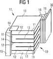
図1には、アクチュエータとして構成された多層構造の圧電式部品10が示されている。ピエゾアクチュエータ10は、多数の圧電セラミック層11と電極層12,13とから成るスタック17を形成している。ここでは、電極層12および13の極性はそれぞれ異なっており、同じ極性の電極層は第1の電極層12と称されるか、ないしは第2の電極層13と称される。同じ極性の電極層12ないしは13はそれぞれ、共通の金属被覆部15ないしは16に結合されている。
FIG. 1 shows a
さらに、非アクティブな絶縁ゾーン14が示されている。この絶縁ゾーン14は、連続した電極層12,13の対向するコーナに交互に配置されている。これらの電極層12,13は、この場合、スタック断面にわたって延在していない。この構成により、すべての第1電極層12ないしはすべての第2電極層13が、それぞれ同じ電極と、垂直な共通の外部金属被覆部15ないしは16によって共通に結合される。外部金属被覆部15,16はたとえば、適切な帯状の金属被覆部である。
In addition, an
金属被覆部16と関連して示されているように、この金属被覆部16は、適した結合手段18を介して付加的接触接続部30に結合されている。前記結合手段18は、たとえばはんだ接合部または溶接接合部等である。同様にして、金属被覆部15も付加的接触接続部(図示されていない)に結合されている。
As shown in connection with the
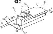
付加的接触接続部30の構成は、図2に示されている。
The configuration of the
図2にはまず、ピエゾアクチュエータ10の積層された層17が「スタック」として、非常に簡単な形態で示されている。スタック17の相互に対向する面には、金属被覆部15,16が設けられており、これらの金属被覆部を介して、スタック17は付加的接触接続部30によって電気的端子エレメント20に接続されている。この端子エレメント20は、たとえば適切な接触ピンである。
In FIG. 2, the
図2に示されているように、付加的接触接続部30はコンタクトエレメント31から成る。このコンタクトエレメント31は、たとえばフィルムである。コンタクトエレメント31はコンタクト領域33を有しており、このコンタクト領域33を介して電気的端子エレメント20との接続が実現される。さらに、コンタクトエレメント31は固定領域34を有し、この固定領域34によって、該コンタクトエレメント31は金属被覆部15,16と結合される。
As shown in FIG. 2, the
ピエゾアクチュエータ10の駆動中には、悪影響を及ぼす機械的な張力/加圧の交番的な負荷が発生し、このような負荷によってコンタクトエレメント31にひびが発生するおそれがある。この負荷を最小にするため、コンタクトエレメント31は少なくとも1つの事前変形部を有している。この事前変形部は、とりわけ撓曲部32である。この実施例では、少なくとも1つの撓曲部32が固定領域34に形成されている。また、少なくとも1つの撓曲部32をコンタクト領域33にも形成するか、または両領域に形成することも考えられる。このような撓曲部32は、撓曲線に沿って形成されたコンタクトエレメント31の事前変形部である。これは、撓曲トルクないしは撓曲応力を負荷することによって形成される。この撓曲部32によって、クリティカルな張力/加圧の交番的な負荷に対して応力変向が行われ、同時に、スタック17から離れたコンタクトエレメント31の領域、ここではコンタクト領域33において応力が減少される。このことによって、コンタクトエレメント31において、疲労によるひびの拡大が緩慢になり、コンタクトエレメント31の最初の半分で、ここでは固定領域34で止められる。このようにして、アクチュエータセラミックスにおいてひびが金属被覆部15,16を分断し、付加的接触接続部30においてひびが発生しても、スタック17の電気的な接触接続を常に保証することができる。
While the
撓曲部32に適した角度は、要求および適用事例に応じて選択される。図2に示された実施例では、撓曲部32に対して、180°の撓曲角度が選択されている。
An angle suitable for the
付加的接触接続部30を本発明によって構成することにより、耐故障性であり、かつピエゾアクチュエータ10の駆動中でも疲労が少ない、スタック17と端子エレメント20との電気的接続を保証することができる。このことはとりわけ、自動車産業において十分に長いピエゾアクチュエータ10の寿命を保証するための中心的な前提である。
By constructing the additional
Claims (6)
圧電セラミック層(11)と電極層(12,13)とが交互に積層されて配置され、スタック(17)が形成されており、
それぞれ、少なくとも1つの第1の電極層(12)、および該スタック(17)において後続する、該第1の電極層に隣接する第2の電極層(13)が、交番的な極性で電気的な接触接続のため、それぞれ、当該スタック(17)と少なくとも1つの電気的端子エレメント(20)とを接続するための少なくとも1つの付加的接触接続部であるコンタクトエレメント(31)に接続されている形式のものにおいて、
前記コンタクトエレメント(31)は、導電性のフィルムとして形成されており、
前記コンタクトエレメント(31)は1つの縁辺側の固定領域(34)において、該圧電式部品の圧電セラミック層の積層方向に沿って前記スタック(17)に結合されており、かつ、該スタック(17)から外側に向かって曲げられており、
前記コンタクトエレメント(31)は、該固定領域(34)と反対側の部分にあり前記積層方向に延在する縁辺側のコンタクト領域(33)において前記少なくとも1つの電気的端子エレメント(20)に結合されていることを特徴とする圧電式部品。A multilayered piezoelectric component,
Piezoelectric ceramic layers (11) and electrode layers (12, 13) are alternately stacked to form a stack (17),
Each of the at least one first electrode layer (12) and the second electrode layer (13) adjacent to the first electrode layer following in the stack (17) is electrically connected with an alternating polarity. Are connected to a contact element ( 31 ), which is at least one additional contact connection for connecting the stack (17) and the at least one electrical terminal element (20), respectively. In the form of
The contact element (31) is formed as a conductive film,
The contact element (31) is coupled to the stack (17) along the stacking direction of the piezoelectric ceramic layers of the piezoelectric component in a fixed region (34) on one edge side, and the stack (17 ) To the outside,
The contact element (31) is coupled to the at least one electrical terminal element (20) in a contact region (33) on a side opposite to the fixing region (34) and extending in the stacking direction. Piezoelectric parts characterized by being made .
各金属被覆部(15,16)は、電気的に前記固定領域(34)に結合されている、請求項1または2記載の圧電式部品。At least one first electrode layer (12) and at least one second electrode layer (13) are each arranged on one side in the stack (17) for electrical contact connection with alternating polarity Connected to at least one metal covering (15, 16);
3. Piezoelectric component according to claim 1 or 2 , wherein each metal covering (15, 16) is electrically coupled to the fixed region (34) .
前記単一の被覆部材はパッシベーション材料から成る、請求項1から4までのいずれか1項記載の圧電式部品。The stack (17) and the contact element ( 31 ) are arranged in a single covering member;
It said single covering member made of Pas Sshibeshon material, any one of claims piezoelectric Shikibu article of claims 1 to 4.
Applications Claiming Priority (2)
| Application Number | Priority Date | Filing Date | Title |
|---|---|---|---|
| DE10131621A DE10131621A1 (en) | 2001-06-29 | 2001-06-29 | Further contact for an electrical component as well as a piezoelectric component in multi-layer construction |
| PCT/EP2002/004723 WO2003005490A2 (en) | 2001-06-29 | 2002-04-29 | Additional contact for an electric component and piezoelectric component in the form of a multilayer structure |
Publications (2)
| Publication Number | Publication Date |
|---|---|
| JP2004534406A JP2004534406A (en) | 2004-11-11 |
| JP4635269B2 true JP4635269B2 (en) | 2011-02-23 |
Family
ID=7690066
Family Applications (1)
| Application Number | Title | Priority Date | Filing Date |
|---|---|---|---|
| JP2003511345A Expired - Lifetime JP4635269B2 (en) | 2001-06-29 | 2002-04-29 | Additional contact connections for multilayered electrical and piezoelectric components |
Country Status (7)
| Country | Link |
|---|---|
| US (1) | US20040169438A1 (en) |
| EP (1) | EP1405372B1 (en) |
| JP (1) | JP4635269B2 (en) |
| CN (1) | CN100342561C (en) |
| DE (2) | DE10131621A1 (en) |
| TW (1) | TW543160B (en) |
| WO (1) | WO2003005490A2 (en) |
Families Citing this family (9)
| Publication number | Priority date | Publication date | Assignee | Title |
|---|---|---|---|---|
| DE10341333B4 (en) * | 2003-09-08 | 2006-06-08 | Siemens Ag | Piezoelectric actuator and method for producing a piezoelectric actuator |
| WO2005035971A1 (en) * | 2003-10-14 | 2005-04-21 | Siemens Aktiengesellschaft | Piezoelectric actuator and associated production method |
| DE102004024867B3 (en) * | 2004-05-19 | 2005-12-22 | Siemens Ag | Method and device for contacting a piezoelectric actuator |
| DE102004028884A1 (en) * | 2004-06-15 | 2006-01-05 | Robert Bosch Gmbh | piezo actuator |
| DE102007046077A1 (en) * | 2007-09-26 | 2009-04-02 | Epcos Ag | Piezoelectric multilayer component |
| DE102009034099A1 (en) * | 2009-07-21 | 2011-01-27 | Epcos Ag | Piezo actuator with electrical contact |
| US9070880B2 (en) * | 2010-12-23 | 2015-06-30 | Lockheed Martin Corporation | Method of manufacturing a tape cast multilayer sonar transducer |
| DE102013106223A1 (en) | 2013-06-14 | 2014-12-18 | Epcos Ag | Multi-layer component with an external contact, a further contact and a connecting element |
| US11442544B2 (en) * | 2017-05-01 | 2022-09-13 | Apple Inc. | Force transducer for electronic devices |
Family Cites Families (10)
| Publication number | Priority date | Publication date | Assignee | Title |
|---|---|---|---|---|
| TW394454U (en) * | 1990-09-14 | 2000-06-11 | Cts Corp | Piezoelectric component-mounting foil |
| JPH04214686A (en) * | 1990-10-05 | 1992-08-05 | Nec Corp | Electrostrictive effect element |
| DE4201937C2 (en) * | 1991-01-25 | 1997-05-22 | Murata Manufacturing Co | Piezoelectric laminated actuator |
| JPH07245431A (en) * | 1994-03-02 | 1995-09-19 | Nippondenso Co Ltd | Multilayer piezoelectric |
| DE19715488C1 (en) * | 1997-04-14 | 1998-06-25 | Siemens Ag | Piezoelectric actuator |
| DE19715487C2 (en) * | 1997-04-14 | 2002-06-13 | Siemens Ag | Piezoelectric actuator with a hollow profile |
| DE19930585B4 (en) * | 1998-08-06 | 2017-11-09 | Epcos Ag | Piezoelectric actuator with improved electrical contacting and use of such a piezoelectric actuator |
| US6144142A (en) * | 1998-11-06 | 2000-11-07 | Face International Corp. | Multi-layer piezoelectric transformer mounting device |
| DE19917728A1 (en) * | 1999-04-20 | 2000-10-26 | Bosch Gmbh Robert | Piezoelectric actuator particularly for operating control valves or injection valves in vehicles, has additional planar electrode strip adjacent actuator body with double comb-type legs |
| EP1065735B1 (en) * | 1999-06-29 | 2007-03-07 | Siemens Aktiengesellschaft | Piezoelectric actuator with a conductive multilayer foil |
-
2001
- 2001-06-29 DE DE10131621A patent/DE10131621A1/en not_active Ceased
-
2002
- 2002-04-29 JP JP2003511345A patent/JP4635269B2/en not_active Expired - Lifetime
- 2002-04-29 DE DE50205209T patent/DE50205209D1/en not_active Expired - Lifetime
- 2002-04-29 US US10/482,206 patent/US20040169438A1/en not_active Abandoned
- 2002-04-29 CN CNB028171160A patent/CN100342561C/en not_active Expired - Lifetime
- 2002-04-29 WO PCT/EP2002/004723 patent/WO2003005490A2/en not_active Ceased
- 2002-04-29 EP EP02730224A patent/EP1405372B1/en not_active Expired - Lifetime
- 2002-05-22 TW TW091110716A patent/TW543160B/en not_active IP Right Cessation
Also Published As
| Publication number | Publication date |
|---|---|
| CN1636301A (en) | 2005-07-06 |
| JP2004534406A (en) | 2004-11-11 |
| WO2003005490A2 (en) | 2003-01-16 |
| TW543160B (en) | 2003-07-21 |
| CN100342561C (en) | 2007-10-10 |
| WO2003005490A3 (en) | 2003-09-25 |
| EP1405372B1 (en) | 2005-12-07 |
| US20040169438A1 (en) | 2004-09-02 |
| DE10131621A1 (en) | 2003-01-23 |
| EP1405372A2 (en) | 2004-04-07 |
| DE50205209D1 (en) | 2006-01-12 |
Similar Documents
| Publication | Publication Date | Title |
|---|---|---|
| US6316863B1 (en) | Piezo actuator with novel contacting and production method | |
| US20090000597A1 (en) | Piezoceramic Multilayer Actuator, Method for Producing a Piezoceramic Multilayer Actuator, and Inujection System | |
| CA2271281A1 (en) | Piezo electric actuator with a new type of contacting and a method for the production thereof | |
| JP4635269B2 (en) | Additional contact connections for multilayered electrical and piezoelectric components | |
| KR20030003250A (en) | Piezoceramic bending transducer and use thereof | |
| CZ2001578A3 (en) | Piezoelectric controller | |
| US6140745A (en) | Motor mounting for piezoelectric transducer | |
| JP2014504010A (en) | Piezo actuator protected from environmental influences | |
| JP4608185B2 (en) | Piezoelectric parts | |
| KR20010072858A (en) | Piezo-multilayer actuator with improved electrode contact | |
| JP2012504858A (en) | Piezoelectric actuator with external electrodes | |
| JPH03174783A (en) | Laminated type piezoelectric element | |
| US10897004B2 (en) | Piezoelectric drive device | |
| JPH04167580A (en) | Laminated piezoelectric actuator element | |
| JP5585730B2 (en) | Multilayer piezoelectric actuator | |
| JP6185661B2 (en) | Multi-layer device having external connection, extension connection, and coupling member | |
| US7679273B2 (en) | Strain tolerant metal electrode design | |
| JP3572208B2 (en) | Multilayer piezoelectric actuator | |
| JP3377922B2 (en) | Multilayer piezoelectric actuator | |
| JP2010103249A (en) | Piezoelectric actuator | |
| JP2001052951A (en) | Ceramic electronic part | |
| JPS61276278A (en) | Laminated piezoelectric material | |
| JPH11214760A (en) | Multilayer piezoelectric actuator | |
| JPH11163426A (en) | Multilayer piezoelectric actuator | |
| JPH11204847A (en) | Multilayer piezoelectric actuator |
Legal Events
| Date | Code | Title | Description |
|---|---|---|---|
| A621 | Written request for application examination |
Free format text: JAPANESE INTERMEDIATE CODE: A621 Effective date: 20050419 |
|
| A131 | Notification of reasons for refusal |
Free format text: JAPANESE INTERMEDIATE CODE: A131 Effective date: 20090116 |
|
| A601 | Written request for extension of time |
Free format text: JAPANESE INTERMEDIATE CODE: A601 Effective date: 20090413 |
|
| A602 | Written permission of extension of time |
Free format text: JAPANESE INTERMEDIATE CODE: A602 Effective date: 20090420 |
|
| A601 | Written request for extension of time |
Free format text: JAPANESE INTERMEDIATE CODE: A601 Effective date: 20090513 |
|
| A602 | Written permission of extension of time |
Free format text: JAPANESE INTERMEDIATE CODE: A602 Effective date: 20090520 |
|
| A601 | Written request for extension of time |
Free format text: JAPANESE INTERMEDIATE CODE: A601 Effective date: 20090615 |
|
| A602 | Written permission of extension of time |
Free format text: JAPANESE INTERMEDIATE CODE: A602 Effective date: 20090622 |
|
| A521 | Request for written amendment filed |
Free format text: JAPANESE INTERMEDIATE CODE: A523 Effective date: 20090716 |
|
| A131 | Notification of reasons for refusal |
Free format text: JAPANESE INTERMEDIATE CODE: A131 Effective date: 20100205 |
|
| A601 | Written request for extension of time |
Free format text: JAPANESE INTERMEDIATE CODE: A601 Effective date: 20100430 |
|
| A602 | Written permission of extension of time |
Free format text: JAPANESE INTERMEDIATE CODE: A602 Effective date: 20100512 |
|
| A601 | Written request for extension of time |
Free format text: JAPANESE INTERMEDIATE CODE: A601 Effective date: 20100602 |
|
| A602 | Written permission of extension of time |
Free format text: JAPANESE INTERMEDIATE CODE: A602 Effective date: 20100609 |
|
| A521 | Request for written amendment filed |
Free format text: JAPANESE INTERMEDIATE CODE: A523 Effective date: 20100705 |
|
| TRDD | Decision of grant or rejection written | ||
| A01 | Written decision to grant a patent or to grant a registration (utility model) |
Free format text: JAPANESE INTERMEDIATE CODE: A01 Effective date: 20100910 |
|
| A01 | Written decision to grant a patent or to grant a registration (utility model) |
Free format text: JAPANESE INTERMEDIATE CODE: A01 |
|
| A601 | Written request for extension of time |
Free format text: JAPANESE INTERMEDIATE CODE: A601 Effective date: 20101008 |
|
| A602 | Written permission of extension of time |
Free format text: JAPANESE INTERMEDIATE CODE: A602 Effective date: 20101018 |
|
| A711 | Notification of change in applicant |
Free format text: JAPANESE INTERMEDIATE CODE: A711 Effective date: 20101102 |
|
| A61 | First payment of annual fees (during grant procedure) |
Free format text: JAPANESE INTERMEDIATE CODE: A61 Effective date: 20101105 |
|
| A521 | Request for written amendment filed |
Free format text: JAPANESE INTERMEDIATE CODE: A821 Effective date: 20101102 |
|
| FPAY | Renewal fee payment (event date is renewal date of database) |
Free format text: PAYMENT UNTIL: 20131203 Year of fee payment: 3 |
|
| R150 | Certificate of patent or registration of utility model |
Ref document number: 4635269 Country of ref document: JP Free format text: JAPANESE INTERMEDIATE CODE: R150 Free format text: JAPANESE INTERMEDIATE CODE: R150 |
|
| R250 | Receipt of annual fees |
Free format text: JAPANESE INTERMEDIATE CODE: R250 |
|
| R250 | Receipt of annual fees |
Free format text: JAPANESE INTERMEDIATE CODE: R250 |
|
| R250 | Receipt of annual fees |
Free format text: JAPANESE INTERMEDIATE CODE: R250 |
|
| R250 | Receipt of annual fees |
Free format text: JAPANESE INTERMEDIATE CODE: R250 |
|
| R250 | Receipt of annual fees |
Free format text: JAPANESE INTERMEDIATE CODE: R250 |
|
| R250 | Receipt of annual fees |
Free format text: JAPANESE INTERMEDIATE CODE: R250 |
|
| R250 | Receipt of annual fees |
Free format text: JAPANESE INTERMEDIATE CODE: R250 |
|
| R250 | Receipt of annual fees |
Free format text: JAPANESE INTERMEDIATE CODE: R250 |
|
| R250 | Receipt of annual fees |
Free format text: JAPANESE INTERMEDIATE CODE: R250 |
|
| EXPY | Cancellation because of completion of term |