JP4631089B2 - Tunable etching diffraction grating for WDM optical communication system - Google Patents
Tunable etching diffraction grating for WDM optical communication system Download PDFInfo
- Publication number
- JP4631089B2 JP4631089B2 JP2001147680A JP2001147680A JP4631089B2 JP 4631089 B2 JP4631089 B2 JP 4631089B2 JP 2001147680 A JP2001147680 A JP 2001147680A JP 2001147680 A JP2001147680 A JP 2001147680A JP 4631089 B2 JP4631089 B2 JP 4631089B2
- Authority
- JP
- Japan
- Prior art keywords
- tunable
- diffraction grating
- waveguide
- refractive index
- optical
- Prior art date
- Legal status (The legal status is an assumption and is not a legal conclusion. Google has not performed a legal analysis and makes no representation as to the accuracy of the status listed.)
- Expired - Fee Related
Links
Images


Classifications
-
- G—PHYSICS
- G02—OPTICS
- G02F—OPTICAL DEVICES OR ARRANGEMENTS FOR THE CONTROL OF LIGHT BY MODIFICATION OF THE OPTICAL PROPERTIES OF THE MEDIA OF THE ELEMENTS INVOLVED THEREIN; NON-LINEAR OPTICS; FREQUENCY-CHANGING OF LIGHT; OPTICAL LOGIC ELEMENTS; OPTICAL ANALOGUE/DIGITAL CONVERTERS
- G02F1/00—Devices or arrangements for the control of the intensity, colour, phase, polarisation or direction of light arriving from an independent light source, e.g. switching, gating or modulating; Non-linear optics
- G02F1/01—Devices or arrangements for the control of the intensity, colour, phase, polarisation or direction of light arriving from an independent light source, e.g. switching, gating or modulating; Non-linear optics for the control of the intensity, phase, polarisation or colour
- G02F1/011—Devices or arrangements for the control of the intensity, colour, phase, polarisation or direction of light arriving from an independent light source, e.g. switching, gating or modulating; Non-linear optics for the control of the intensity, phase, polarisation or colour in optical waveguides, not otherwise provided for in this subclass
- G02F1/0115—Devices or arrangements for the control of the intensity, colour, phase, polarisation or direction of light arriving from an independent light source, e.g. switching, gating or modulating; Non-linear optics for the control of the intensity, phase, polarisation or colour in optical waveguides, not otherwise provided for in this subclass in optical fibres
-
- G—PHYSICS
- G02—OPTICS
- G02F—OPTICAL DEVICES OR ARRANGEMENTS FOR THE CONTROL OF LIGHT BY MODIFICATION OF THE OPTICAL PROPERTIES OF THE MEDIA OF THE ELEMENTS INVOLVED THEREIN; NON-LINEAR OPTICS; FREQUENCY-CHANGING OF LIGHT; OPTICAL LOGIC ELEMENTS; OPTICAL ANALOGUE/DIGITAL CONVERTERS
- G02F1/00—Devices or arrangements for the control of the intensity, colour, phase, polarisation or direction of light arriving from an independent light source, e.g. switching, gating or modulating; Non-linear optics
- G02F1/01—Devices or arrangements for the control of the intensity, colour, phase, polarisation or direction of light arriving from an independent light source, e.g. switching, gating or modulating; Non-linear optics for the control of the intensity, phase, polarisation or colour
- G02F1/0147—Devices or arrangements for the control of the intensity, colour, phase, polarisation or direction of light arriving from an independent light source, e.g. switching, gating or modulating; Non-linear optics for the control of the intensity, phase, polarisation or colour based on thermo-optic effects
-
- G—PHYSICS
- G02—OPTICS
- G02F—OPTICAL DEVICES OR ARRANGEMENTS FOR THE CONTROL OF LIGHT BY MODIFICATION OF THE OPTICAL PROPERTIES OF THE MEDIA OF THE ELEMENTS INVOLVED THEREIN; NON-LINEAR OPTICS; FREQUENCY-CHANGING OF LIGHT; OPTICAL LOGIC ELEMENTS; OPTICAL ANALOGUE/DIGITAL CONVERTERS
- G02F1/00—Devices or arrangements for the control of the intensity, colour, phase, polarisation or direction of light arriving from an independent light source, e.g. switching, gating or modulating; Non-linear optics
- G02F1/01—Devices or arrangements for the control of the intensity, colour, phase, polarisation or direction of light arriving from an independent light source, e.g. switching, gating or modulating; Non-linear optics for the control of the intensity, phase, polarisation or colour
- G02F1/061—Devices or arrangements for the control of the intensity, colour, phase, polarisation or direction of light arriving from an independent light source, e.g. switching, gating or modulating; Non-linear optics for the control of the intensity, phase, polarisation or colour based on electro-optical organic material
- G02F1/065—Devices or arrangements for the control of the intensity, colour, phase, polarisation or direction of light arriving from an independent light source, e.g. switching, gating or modulating; Non-linear optics for the control of the intensity, phase, polarisation or colour based on electro-optical organic material in an optical waveguide structure
-
- G—PHYSICS
- G02—OPTICS
- G02F—OPTICAL DEVICES OR ARRANGEMENTS FOR THE CONTROL OF LIGHT BY MODIFICATION OF THE OPTICAL PROPERTIES OF THE MEDIA OF THE ELEMENTS INVOLVED THEREIN; NON-LINEAR OPTICS; FREQUENCY-CHANGING OF LIGHT; OPTICAL LOGIC ELEMENTS; OPTICAL ANALOGUE/DIGITAL CONVERTERS
- G02F2201/00—Constructional arrangements not provided for in groups G02F1/00 - G02F7/00
- G02F2201/30—Constructional arrangements not provided for in groups G02F1/00 - G02F7/00 grating
- G02F2201/307—Reflective grating, i.e. Bragg grating
Description
【0001】
【発明の属する技術分野】
本発明は光導波路回折格子、より詳細には、とりわけ、光通信システムに対する追加/ドロップフィルタ、回折格子支援結合器および可変遅延ラインに用いるのに適するエッチングにて形成される導波路回折格子に関する。
【0002】
【従来の技術】
光回折格子は、光通信システム内で特定の波長の光を選択的に制御するために重要な要素である。光回折格子には、ブラッグ回折格子と長周期回折格子がある。回折格子は、典型的には、材料の本体と、複数の実質的に等間隔に配置された光回折格子要素、例えば、屈折率摂動、スリット、あるいは溝(グルーブ)から構成される。
【0003】
典型的なブラッグ回折格子はある長さの光導波路を含み、この導波路の長さ方向に沿って複数の実質的に等間隔の屈折率の摂動が設けられる。これら摂動は一連の摂動間の間隔Λに有効屈折率を掛けた値の二倍に等しい波長λ、つまり、λ=2neffΛの光を選択的に反射する。ここで、λは真空中の波長を表し、neffは基本モードの有効屈折率を表す。残りの波長(の光)は実質的に妨害されることなく通過する。このようなブラッグ回折格子は、フィルタリング、光信号チャネルの追加およびドロップ、半導体レーザの安定化、ファイバ増幅器ポンプエネルギーの反射、分散の補償などを含む多様な用途に用いられている。
【0004】
【発明が解決しようとする課題】
従来のブラッグ回折格子と関連する一つの問題は、これらがある固定の波長しかフィルタリングできないことである。各回折格子は、λ=2neffΛを中心とする狭い帯域幅内の光のみを選択的に反射する。ただし、多くの用途、例えば、波長分割多元(WDM)においては、波長応答を制御下で変更することができる再構成可能な(リコンフィガラブル)回折格子が要望されている。
【0005】
長周期回折格子デバイスは波長に依存する損失を提供し、スペクトルの成形に用いられる。長周期回折格子は、光電力を、2つの同時に伝搬するモード間で、後方反射を殆ど伴うことなく結合する。長周期回折格子は、典型的には、ある長さの光導波路から成り、この導波路に沿って複数の屈折率摂動が伝送される光の波長λと比べて大きな周期距離Λ’だけ離して配置される。従来のブラッグ回折格子とは対照的に、長距離回折格子は、典型的には、少なくとも伝送される波長の10倍より大きな周期間隔、つまり、Λ’≧10λなる周期間隔を用いる。典型的には、Λ’は15〜1500マイクロメータのレンジとされ、摂動の幅は1/5Λ’〜4/5Λ’のレンジとされる。幾つかの用途、例えば、チャープド回折格子においては、間隔Λ’は回折格子の長さ方向に沿って変えられる。
【0006】
長周期回折格子デバイスは、特定の波長の光をモード変換によって除去する。
光が反射され、導波路内にとどまる従来のブラッグ回折格子とは対照的に、長距離回折格子は、特定の波長の光を、反射によってではなく、ガイドモードから非ガイドモードに変換することで除去する。(非ガイドモードとはコア内に拘束されるのではなく、導波路構造全体によって制限されるモードを意味する。しばしば、非ガイドモードはクラッドモードである)。摂動の間隔Λ’は、選択されたピーク波長λpの領域内の伝送される光が非ガイドモードに変換され、これによってλpを中心とするバンドの光の強度が低減されるように選択される。代替として、間隔Λ’は、あるガイドモードからの光を除去される第二のガイドモード(典型的にはより高次のモード)にシフトするように選択されることもある。
【0007】
ただし、従来の長周期回折格子の一つの短所として、これら回折格子は利得を動的に等化する能力に欠ける。これら回折格子は、固定された波長しかフィルタリングすることができない。ある与えられた周期(Λ’)を持つ各長周期回折格子は、λp=(ng−nng)・Λ’を中心とする狭い帯域幅内の光しかフィルタリングすることができない。ここで、ngとnngは、それぞれ、コアモードとクラッドモードの有効屈折率を表す。ngの値はコアとクラッドの屈折率に依存し、nngは、コア、クラッド、および空気の屈折率に依存する。
【0008】
回折格子をチューニングするための様々な技法が開発されており、チューナブル回折格子の重要な用途には、光通信システム用のチューナブル追加/ドロップフィルタの製造が含まれる。チューナブルフィルタは、WDMシステムにおいて、システムの端末もしくは中間点においてチャネルを追加あるいはドロップするために広く用いられている。これらチューナブルフィルタは、平坦な通過帯域および良好な阻止帯域特性を要求される。典型的には、光ファイバあるいはプレーナ導波路内に書き込まれたUV光誘導ブラッグ回折格子が、優れたスペクトル特性を持つという理由から採用される。ファイバ内にチューナブルブラッグ回折格子を形成するための多くの技法、例えば、温度やストレッチングを応用する技法が導入されている。チューナブルフィルタがシステム内で再構成される際、動作はシステム内の他のチャネルに対して透過的(トランスパレント)であるべきである。つまり、ヒットレス再構成が要望される。これは、現在のチューナブル回折格子では、再構成の際に回折格子をバイパスするためにスイッチを用いない限り、不可能である。代替においては、回折格子はチャネル間内にフィットするために十分に狭い帯域幅を持つことを要求される。このことは、回折格子が隣接チャネルに対して透過的となるように、回折格子が極端に良好な特性を持つことを要求する。
【0009】
【課題を解決するための手段】
本発明によると、導波路回折格子は、コアと、コアに隣接する第一のクラッド材を含む。第一のクラッド材は、例えば、エッチングによって、周期回折格子を持つように構成される。第一のクラッド材を覆うように制御可能な屈折率を持つ第二のクラッド材が配置される。第二のクラッドの屈折率が第一のクラッドの屈折率と異なるときは、第一のクラッドの構成は光回折格子(作用)を提供する。ただし、第二のクラッドの制御可能な屈折率が第一のクラッドの屈折率と等しくなるように調節されたときは、回折格子は実質的に透過的となる。この回折格子は、とりわけ、WDM光通信システム内の再構成可能な(リコンフィガラブル)追加/ドロップフィルタとして有効である。この回折格子は、加えて、回折格子支援結合器および可変光遅延ライン内に用いることもできる。
【0010】
本発明の長所、性質および様々な追加の特徴が、以下に詳細に説明する実施例から一層明らかになるものである。図面は単に本発明の概念を説明するためのもので、グラフを除いては、正確な縮尺には描かれてないことに注意する。
【0011】
【発明の実施の形態】
図1は、チューナブル導波路回折格子10の略断面図を示す。チューナブル導波路回折格子10は屈折率n1を持つコア11を含み、コア11の周囲には、屈折率n1より小さな屈折率、例えば、それぞれ、屈折率n2、n3を持つクラッド層12A、12Bが配置される。クラッド層12Bの一部分は、例えば、エッチングによって、周期回折格子13を形成する空間変動が達成されるように構成される。n1より小さな屈折率n3を持つ第二のクラッド層14が第一のクラッド層12Bを覆い、回折格子13を満たすように設けられる。このデバイスはプレーナ導波路回折格子あるいはファイバ回折格子のいずれとすることもできる。図1に示すプレーナ導波路形態とされる場合は、このデバイスは、好ましくは、支持基板15上に形成される。回折格子13は伝送される光の波長と回折格子間隔との関係によってブラッグ(Bragg)回折格子あるいは長周期回折格子のいずれとすることもできる。
【0012】
本発明によると、クラッド12A、12B、14は、n2あるいはn3が独立に制御できるような材料から作られる。より具体的には、このデバイスは、少なくとも2つの状態、つまり、1)n2≠n3、および2)n2=n3の間でチューニングすることができる。第一の状態、つまり、n2≠n3においては、この周期構造は光回折格子として機能する。第二の状態、つまり、n2=n3においては、回折格子は光学的に透過的となり、伝送される光には殆ど影響を与えない。
【0013】
回折格子を2つの状態の間でチューニングするための好ましい機構においては、クラッドの一方は、他方のクラッドと比較して屈折率が温度とともにより大きく変動する材料から作くられる。例えば、クラッド12Bはシリカから形成され、第二のクラッド14はより温度に敏感な屈折率を持つポリマーから形成される。第二のクラッド14に熱的に結合された抵抗加熱要素16によって所望のチューニングが達成される。
【0014】
代替として、回折格子をこれら2つの状態の間でチューニングするために、クラッドの一方をエレクトロオプテックあるいは液晶材料から作り、電場を加えて制御することもできる。クラッドの一方を半導体材料から作り、電荷の注入あるいは涸渇によって屈折率をチューニングすることもできる。さらに、クラッドの一方を磁気光学材料から作り、磁場によってチューニングすることも、あるいはガラスから作り、屈折率を応力によってチューニングすることも考えられる。
【0015】
以下では本発明の理解を含めるために、本発明の具体例について説明する。
例
一つの実施例においては、基板16はシリコンから成る。クラッド12A、12Bは、Geをドープされたシリカから成り、コア11はより屈折率の高いドープされたシリカから形成される。回折格子13は、クラッド12B内のエッチングされ、はざまを設けられた、領域として形成される。第二のクラッド14は、ポリマー、例えば、ハロゲン化アクリル酸樹脂から成る。
【0016】
シリカベースの層が用いられた場合の1.55マイクロメータなる波長における屈折率は:クラッド12A、1.445;コア11、1.46234;クラッド12B、1.44512とされる。ブラッグ回折格子の場合、クラッド層の厚さは、1.1マイクロメータとされ、エッチングの深さは1.0マイクロメータとされ、周期Λは、λ/2e=530ナノメートルとされる。ここで、ne=1.4511は、有効屈折率を表す。ポリマーから成る上側クラッドは-4×10−4/℃なる屈折率温度依存性を持つ。
【0017】
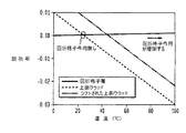
図2は、一例としてのデバイスの動作の理解を助けるために、クラッド層の屈折率を温度の関数として示す。ポリマー(クラッド層)14の屈折率が回折格子層のクラッド12Bの屈折率と一致するように(図2において円によって示されるように)温度が設定された場合は、回折格子は透過的となる。温度が増加すると、ポリマーの屈折率は低下し、回折格子(作用)の強さは増加する。温度が73℃変化すると屈折率も変化するが、このとき、回折格子の強度はδne/ne=1×10−3に比例して変化する。反射帯域幅は回折格子強度とΔ≒λδne/neなる係数にて比例し、これらパラメータにて、最高約1nmまでの帯域幅を達成することができる。この回折格子強度は、従って、WDM通信システムにおけるフィルタとして十分である。
【0018】
図1のチューナブル回折格子はたった一つのコア制限導波路(core-defined waveguide)との関連で用いられるが、図1の回折格子をより複雑な導波路構造と共に用いることもできる。例えば、図3Aおよび図3Bは、それぞれ、チューナブル回折格子10A、10Bを用いる回折格子支援結合器を示す略正面図を示す。図3Aは、光学的に結合されたペアの導波路コア31Aおよび31Bと、結合領域を覆うように設けられたチューナブルブラッグ回折格子10Aから構成されるブラッグ回折格子支援結合器30を示す。回折格子共振に対応する波長λcの出力は図示されるように反射する。結合強度は、回折格子の屈折率定数をチューニングすることで変えることができる。
【0019】
図3Bは、ペアの光学的に結合された導波路コア31Aおよび31Bと、結合領域を覆うように設けられたチューナブル長周期回折格子10Bから構成される長周期回折格子支援結合器33を示す。順方向シフトモードに対応する波長λcの出力は図示するように伝送される。ここでも、結合強度はクラッドの屈折定数をチューニングすることで、変えることができる。
【0020】
図4は、図1との関連で説明したチューナブル導波路回折格子10を用いるチューナブルオールパスフィルタ40を簡略的に示す。フィルタ40は、導波リング共振器42の近傍を通過するある長さの導波路41を含む。導波路41とリング共振器42は、互いに、結合領域43において、これらが運ぶ光のテールが指数関数的に重複するほど十分に接近される。チューナブル導波路回折格子10は、結合領域43を覆うように設けられる。回折格子10はブラッグ回折格子あるいは長周期回折格子のいずれとすることもできる。好ましくは、位相シフタ44、例えば、抵抗加熱器がリング共振器42に結合される。
【0021】
このデバイスは、動作においては、チューナブルオールパスフィルタとして機能する。回折格子10がブラッグ回折格子とされる場合は、入力からの光は、反射によって、回折格子10から時計方向にリング42を回りを回折格子10へと結合され、ここから出力に向けて反射される。回折格子10が長周期回折格子とされる場合は、入力は、順方向にリング42へと結合される。その後、この入力は、リングの回りを反時計方向に進み、導波路41内に結合され、出力に向って順方向に進む。
【0022】
導波路とリングとの間の結合強度のチューニングは、回折格子10を関連する加熱器16を介して制御することで達成される。リング42の共振波長のチューニングは、位相シフタ44を制御することで達成される。
【0023】
図5は、図1のペアのチューナブル導波路回折格子10A、10Bを用いるチューナブルドロップフィルタ50を簡略的に示す。ドロップフィルタ50は、ペアの導波路41A、41Bを含み、これら導波路は各々の結合領域43A、43Bの所で、導波リング共振器42の近傍を通過する。チューナブル導波路回折格子10A、10Bが、各々の結合領域43A、43Bを覆うように配置される。回折格子10A、10Bは、両方ともブラッグ回折格子とすることも、あるいは両方とも長周期回折格子とすることもできる。好ましくは、位相シフタ44、例えば、抵抗加熱器がリング共振器42に結合される。
【0024】
このデバイスは、動作においては、チューナブルドロップフィルタとして機能する。回折格子10Aと10Bが両方ともドロップされるべき波長λにチューナブルされたブラッグ回折格子である場合は、入力導波路41Aから回折格子10Aに到着する波長λは、反射によって、時計方向にリング42に結合される。回折格子10Bに到着すると、これは反射によって、出力導波路41Bに結合される。これら回折格子が両方とも長周期回折格子である場合は、順方向結合によって類似の結果が達成される。
【0025】
図6は、図1に示す複数のチューナブル導波路回折格子10A、10B、10Cを用いる代替のドロップフィルタ60を示す。ドロップフィルタ60は、ペアの概ね平行な導波路61、62を含み、複数の結合領域43A、43B、43Cを持つ。これら各結合領域を覆うように回折格子10A、10B、10Cが配置される。好ましくは、位相シフタ44A、44B、44Cが各ペアの回折格子の間に導波路62(図面では61)に結合される。回折格子10A、10B、10Cはブラッグ回折格子から成り、導波路61、62は、好ましくは、大きく異なる屈折率(例えば、2.0と1.4)を持つ。
【0026】
動作においては、広帯域信号が入力導波路61に入る。回折格子10A、10B、10Cがドロップ波長λにチューナブルされている場合は、信号が回折格子に到着すると、ドロップ波長は、反射的にドロップ導波路62に結合される。位相シフタ44Aと44Bによって、一連の反射の間の位相関係がチューニングされ、導波路の異なる有効屈折率のために後方反射が最小限に押さえられる。導波路61上の非ドロップ成分は出力に寄与する。
【0027】
図7は、図1の回折格子の変形を用いるチューナブル光遅延ラインの略断面図である。図7のデバイスは図1のデバイスと類似するが、回折格子13を覆うように単一の屈折率制御要素を配置される代わりに、回折格子13の長さに方向に沿ってこれを覆うように一連の制御要素16A〜16Pが配置される点が異なる。
【0028】
図7のデバイスは、公称温度においては、回折格子は透過的であり、導波路として機能する。クラッド14のセクションを局所的に加熱すると、回折格子が現れ、回折格子共振の所の入力信号は反射される。回折格子は、上流の加熱器をチューニングオフし、下流の加熱器をチューニングオンすることで、下方に移動させることができる。すると、信号によって反射の前に経験される遅延は増加する。
【0029】
上述の実施例は単に本発明の原理の適用を表す多くの可能な実施例の僅かな例に過ぎず、当業者においては、本発明の精神および範囲から逸脱することなく、様々な他の修正された構成を容易に考案できるものである。
【図面の簡単な説明】
【図1】チューナブル導波路回折格子の略断面図である。
【図2】デバイスの動作を理解するために有効な図1のデバイスの要素の屈折率を示すグラフである。
【図3】AおよびBは図1のチューナブル回折格子を用いる回折格子支援結合器を簡略的に示す図である。
【図4】図1の回折格子を用いるチューナブルオールパスフィルタを簡略的に示す図である。
【図5】図1の回折格子を用いるチューナブルドロップフィルタを簡略的に示す図である。
【図6】図1の回折格子を用いる代替のドロップフィルタを示す図である。
【図7】図1の回折格子を用いる可変光遅延ラインを示す図である。
【符号の説明】
10 チューナブル(チューナブル)導波路回折格子
11 コア
12A、12B クラッド層
14 第二のクラッド層
13 周期回折格子
15 支持基板
16 抵抗加熱要素
30 ブラッグ回折格子支援結合器
33 長周期回折格子支援結合器
40 チューナブルオールパスフィルタ
41 導波路
42 導波路リング共振器
43 結合領域
44 位相シフタ
50 チューナブル(チューナブル)ドロップフィルタ[0001]
BACKGROUND OF THE INVENTION
The present invention relates to optical waveguide diffraction gratings, and more particularly to waveguide diffraction gratings formed by etching suitable for use in add / drop filters, diffraction grating assisted couplers and variable delay lines for optical communication systems.
[0002]
[Prior art]
An optical diffraction grating is an important element for selectively controlling light of a specific wavelength in an optical communication system. The optical diffraction grating includes a Bragg diffraction grating and a long-period diffraction grating. A diffraction grating typically consists of a body of material and a plurality of substantially equally spaced optical diffraction grating elements, such as refractive index perturbations, slits, or grooves.
[0003]
A typical Bragg grating includes a length of optical waveguide, and a plurality of substantially equally spaced index perturbations are provided along the length of the waveguide. These perturbations selectively reflect light having a wavelength λ equal to twice the interval Λ between the series of perturbations multiplied by the effective refractive index, ie, λ = 2n eff Λ. Here, λ represents the wavelength in vacuum, and n eff represents the effective refractive index of the fundamental mode. The remaining wavelengths pass through substantially unimpeded. Such Bragg gratings are used in a variety of applications including filtering, adding and dropping optical signal channels, stabilizing a semiconductor laser, reflecting fiber amplifier pump energy, compensating for dispersion, and the like.
[0004]
[Problems to be solved by the invention]
One problem associated with conventional Bragg gratings is that they can only filter certain fixed wavelengths. Each diffraction grating selectively reflects only light within a narrow bandwidth centered at λ = 2n eff Λ. However, in many applications, such as wavelength division multiple (WDM), there is a need for a reconfigurable grating that can change the wavelength response under control.
[0005]
Long period grating devices provide wavelength dependent loss and are used for spectral shaping. Long period gratings couple optical power between two simultaneously propagating modes with little back reflection. A long-period grating typically consists of an optical waveguide of a certain length, separated by a large periodic distance Λ ′ compared to the wavelength λ of the light along which multiple refractive index perturbations are transmitted. Be placed. In contrast to conventional Bragg gratings, long-range gratings typically use a period interval that is at least greater than 10 times the transmitted wavelength, ie, a period interval of Λ ′ ≧ 10λ. Typically, Λ ′ is in the range of 15 to 1500 micrometers and the perturbation width is in the range of 1 / 5Λ ′ to 4 / 5Λ ′. In some applications, such as chirped diffraction gratings, the spacing Λ ′ can be varied along the length of the diffraction grating.
[0006]
A long-period grating device removes light of a specific wavelength by mode conversion.
In contrast to conventional Bragg gratings, where light is reflected and stays in the waveguide, long-range gratings convert certain wavelengths of light from a guided mode to a non-guided mode rather than by reflection. Remove. (Non-guided mode refers to a mode that is not constrained within the core but limited by the entire waveguide structure. Often the non-guided mode is a cladding mode). The perturbation interval Λ ′ is selected so that the transmitted light in the region of the selected peak wavelength λ p is converted to a non-guided mode, thereby reducing the intensity of light in the band centered on λ p Is done. Alternatively, the interval Λ ′ may be selected to shift to a second guide mode (typically a higher order mode) that removes light from one guide mode.
[0007]
However, as one disadvantage of conventional long-period diffraction gratings, these diffraction gratings lack the ability to dynamically equalize gain. These diffraction gratings can only filter a fixed wavelength. Each long-period grating with a given period (Λ ′) can only filter light within a narrow bandwidth centered at λ p = (n g −n ng ) · Λ ′. Here, n g and n ng, respectively, represent the effective refractive index of the core mode and the cladding mode. The value of n g is dependent on the refractive index of the core and the cladding, n ng depends core, cladding, and the refractive index of air.
[0008]
Various techniques have been developed for tuning diffraction gratings, and important applications for tunable diffraction gratings include the manufacture of tunable add / drop filters for optical communication systems. Tunable filters are widely used in WDM systems to add or drop channels at system terminals or midpoints. These tunable filters are required to have a flat passband and good stopband characteristics. Typically, UV light-guided Bragg gratings written in optical fibers or planar waveguides are employed because they have excellent spectral characteristics. Many techniques have been introduced to form tunable Bragg gratings in the fiber, such as techniques that apply temperature and stretching. When a tunable filter is reconfigured in the system, the operation should be transparent to other channels in the system. That is, hitless reconstruction is desired. This is not possible with current tunable diffraction gratings unless a switch is used to bypass the diffraction grating during reconstruction. In the alternative, the diffraction grating is required to have a sufficiently narrow bandwidth to fit within the channel. This requires that the diffraction grating has extremely good characteristics so that the diffraction grating is transparent to the adjacent channel.
[0009]
[Means for Solving the Problems]
According to the present invention, the waveguide diffraction grating includes a core and a first cladding material adjacent to the core. The first cladding material is configured to have a periodic diffraction grating by, for example, etching. A second cladding material having a controllable refractive index is disposed to cover the first cladding material. When the refractive index of the second cladding is different from the refractive index of the first cladding, the configuration of the first cladding provides an optical diffraction grating (action). However, when the controllable refractive index of the second cladding is adjusted to be equal to the refractive index of the first cladding, the diffraction grating becomes substantially transparent. This diffraction grating is particularly useful as a reconfigurable add / drop filter in a WDM optical communication system. This diffraction grating can also be used in diffraction grating assisted couplers and variable optical delay lines.
[0010]
The advantages, properties and various additional features of the present invention will become more apparent from the examples described in detail below. Note that the drawings are merely for the purpose of illustrating the concepts of the invention and are not drawn to scale except for graphs.
[0011]
DETAILED DESCRIPTION OF THE INVENTION
FIG. 1 shows a schematic cross-sectional view of a tunable
[0012]
According to the present invention, the
[0013]
In a preferred mechanism for tuning the diffraction grating between two states, one of the claddings is made from a material whose refractive index varies more with temperature compared to the other cladding. For example, the cladding 12B is formed from silica, and the
[0014]
Alternatively, to tune the diffraction grating between these two states, one of the claddings can be made from electro-optic or liquid crystal material and controlled by applying an electric field. One of the claddings can be made of a semiconductor material and the refractive index can be tuned by charge injection or depletion. Further, it is conceivable that one of the clads is made of a magneto-optical material and tuned by a magnetic field, or made of glass and the refractive index is tuned by stress.
[0015]
Hereinafter, specific examples of the present invention will be described in order to include an understanding of the present invention.
Example In one embodiment, the
[0016]
The refractive indices at a wavelength of 1.55 micrometers when a silica-based layer is used are: clad 12A, 1.445;
[0017]
FIG. 2 shows the refractive index of the cladding layer as a function of temperature to aid in understanding the operation of the example device. When the temperature is set so that the refractive index of the polymer (cladding layer) 14 matches the refractive index of the cladding 12B of the diffraction grating layer (as indicated by the circle in FIG. 2), the diffraction grating becomes transparent. . As the temperature increases, the refractive index of the polymer decreases and the strength of the diffraction grating (action) increases. When the temperature changes by 73 ° C., the refractive index also changes. At this time, the intensity of the diffraction grating changes in proportion to δn e / n e = 1 × 10 −3 . The reflection bandwidth is proportional to the diffraction grating intensity and the coefficient Δ≈λδn e / n e , and with these parameters, a bandwidth up to about 1 nm can be achieved. This diffraction grating intensity is therefore sufficient as a filter in a WDM communication system.
[0018]
Although the tunable diffraction grating of FIG. 1 is used in conjunction with a single core-defined waveguide, the diffraction grating of FIG. 1 can also be used with more complex waveguide structures. For example, FIGS. 3A and 3B show schematic front views illustrating a diffraction grating assisted coupler using
[0019]
FIG. 3B shows a long-period diffraction grating assisted
[0020]
FIG. 4 schematically illustrates a tunable all-
[0021]
In operation, this device functions as a tunable all-pass filter. When the
[0022]
Tuning the coupling strength between the waveguide and the ring is accomplished by controlling the
[0023]
FIG. 5 schematically shows a
[0024]
This device functions as a tunable drop filter in operation. If both
[0025]
FIG. 6 shows an
[0026]
In operation, a broadband signal enters the input waveguide 61. If the
[0027]
FIG. 7 is a schematic cross-sectional view of a tunable optical delay line using a modification of the diffraction grating of FIG. The device of FIG. 7 is similar to the device of FIG. 1, but instead of placing a single refractive index control element over the
[0028]
In the device of FIG. 7, at the nominal temperature, the diffraction grating is transparent and functions as a waveguide. When the section of the
[0029]
The above-described embodiments are merely a few examples of the many possible embodiments that represent the application of the principles of the present invention, and various other modifications will occur to those skilled in the art without departing from the spirit and scope of the invention. It is possible to easily devise the structure.
[Brief description of the drawings]
FIG. 1 is a schematic cross-sectional view of a tunable waveguide diffraction grating.
FIG. 2 is a graph showing the refractive indices of elements of the device of FIG. 1 that are useful for understanding the operation of the device.
FIGS. 3A and 3B are diagrams schematically showing a diffraction grating assisted coupler using the tunable diffraction grating of FIG. 1;
4 is a diagram schematically showing a tunable all-pass filter using the diffraction grating of FIG. 1. FIG.
5 is a diagram schematically showing a tunable drop filter using the diffraction grating of FIG. 1. FIG.
6 shows an alternative drop filter using the diffraction grating of FIG. 1. FIG.
7 is a diagram showing a variable optical delay line using the diffraction grating of FIG. 1; FIG.
[Explanation of symbols]
10
Claims (17)
コア領域、および周囲を取り巻く、屈折率を持つ第一の材料から作られた第一のクラッドを含む光導波路と、
前記コアの長さ方向に沿って隣接して配置された周期的空間変動を提供するように構成された、前記第一のクラッドの前記コア領域に隣接する部分と、
前記第一の材料の屈折率に関して調節可能な屈折率を持ち、前記空間変動を覆って前記空間変動間に配置された、前記第一の材料と異なる第二の材料から作られた第二のクラッドと、
前記光導波路に沿って伝送する光に光回折格子として作用する屈折率不等の状態と光回折格子として作用しない屈折率同等の状態との間で、前記第二のクラッドと第一のクラッドとの間の屈折率の差を両状態に調節するよう構成された制御要素とを備えることを特徴とするチューナブル回折格子。A tunable optical diffraction grating,
An optical waveguide including a core region, and surrounding the circumference, the first cladding made from a first material having a refractive index,
A portion adjacent to the core region of the first cladding configured to provide periodic spatial variation disposed adjacently along a length of the core;
Has an adjustable refractive index with respect to the refractive index of the first material, said I covering the spatial variation arranged between spatial variation, the second made from the first material and the second material different A clad of
Between the second clad and the first clad between a refractive index unequal state that acts as an optical diffraction grating on light transmitted along the optical waveguide and an equivalent refractive index state that does not act as an optical diffraction grating ; And a control element configured to adjust the difference in refractive index between the two states .
導波路リング共振器と、
第一の結合領域に沿って前記共振器の近傍を通る第一の導波路と、
第二の結合領域に沿って前記共振器の近傍を通る第二の導波路と、
それぞれ、前記第一と第二の結合領域を覆うように配置された請求項1記載の第一および第二のチューナブル回折格子とを備えることを特徴とするチューナブルドロップフィルタ。A tunable drop filter,
A waveguide ring resonator;
A first waveguide passing through the vicinity of the resonator along a first coupling region;
A second waveguide passing in the vicinity of the resonator along a second coupling region;
A tunable drop filter comprising: the first and second tunable diffraction gratings according to claim 1, each of which is disposed so as to cover the first and second coupling regions.
複数の光結合領域を持つ第一と第二の概ね平行な導波路;および
請求項1記載の複数のチューナブル回折格子を含み、各回折格子がブラッグ回折格子から成り、各々の光結合領域を覆うように配置されることを特徴とするチューナブルドロップフィルタ。A tunable drop filter,
A first and a second generally parallel waveguide having a plurality of optical coupling regions; and a plurality of tunable diffraction gratings according to claim 1, wherein each diffraction grating comprises a Bragg diffraction grating, A tunable drop filter characterized by being arranged to cover.
Applications Claiming Priority (2)
| Application Number | Priority Date | Filing Date | Title |
|---|---|---|---|
| US09/573988 | 2000-05-17 | ||
| US09/573,988 US6522795B1 (en) | 2000-05-17 | 2000-05-17 | Tunable etched grating for WDM optical communication systems |
Publications (3)
| Publication Number | Publication Date |
|---|---|
| JP2002014307A JP2002014307A (en) | 2002-01-18 |
| JP2002014307A5 JP2002014307A5 (en) | 2008-06-26 |
| JP4631089B2 true JP4631089B2 (en) | 2011-02-16 |
Family
ID=24294223
Family Applications (1)
| Application Number | Title | Priority Date | Filing Date |
|---|---|---|---|
| JP2001147680A Expired - Fee Related JP4631089B2 (en) | 2000-05-17 | 2001-05-17 | Tunable etching diffraction grating for WDM optical communication system |
Country Status (4)
| Country | Link |
|---|---|
| US (1) | US6522795B1 (en) |
| EP (1) | EP1158342B1 (en) |
| JP (1) | JP4631089B2 (en) |
| DE (1) | DE60133853D1 (en) |
Families Citing this family (60)
| Publication number | Priority date | Publication date | Assignee | Title |
|---|---|---|---|---|
| US6858834B2 (en) * | 2000-10-18 | 2005-02-22 | Fibera, Inc. | Light wavelength meter |
| US6795459B2 (en) | 2000-10-18 | 2004-09-21 | Fibera, Inc. | Light frequency locker |
| US6856641B2 (en) * | 2001-01-26 | 2005-02-15 | California Institute Of Technology | Ring resonator based narrow-linewidth semiconductor lasers |
| US6748138B2 (en) * | 2001-09-14 | 2004-06-08 | Fibera, Inc. | Optical grating fabrication |
| US6807339B1 (en) * | 2001-09-14 | 2004-10-19 | Fibera, Inc. | Wavelength division multiplexing and de-multiplexing system |
| US6804060B1 (en) | 2001-09-28 | 2004-10-12 | Fibera, Inc. | Interference filter fabrication |
| US6973231B2 (en) * | 2001-10-22 | 2005-12-06 | International Optics Communications Corporation | Waveguide grating-based wavelength selective switch actuated by thermal mechanism |
| US20030179998A1 (en) * | 2002-03-22 | 2003-09-25 | Jianjun Zhang | Switchable bragg grating filter |
| US6891989B2 (en) * | 2001-10-22 | 2005-05-10 | Integrated Optics Communications Corporation | Optical switch systems using waveguide grating-based wavelength selective switch modules |
| GB2382569A (en) * | 2001-11-30 | 2003-06-04 | Yew Tree Consultants Ltd | A closure fitment for sealing a foodstuffs container |
| US6879754B2 (en) * | 2001-12-10 | 2005-04-12 | Integrated Optics Communications Corporation | Drop-before-add optical switching and routing system employing grating-based wavelength selective switches |
| US20030108290A1 (en) * | 2001-12-10 | 2003-06-12 | Jianjun Zhang | Optical add/drop devices employing waveguide grating-based wavelength selective switches |
| US20030123798A1 (en) * | 2001-12-10 | 2003-07-03 | Jianjun Zhang | Wavelength-selective optical switch with integrated Bragg gratings |
| JP3747241B2 (en) * | 2002-01-17 | 2006-02-22 | 独立行政法人情報通信研究機構 | Variable optical delay device |
| US6671437B2 (en) * | 2002-05-08 | 2003-12-30 | Lambda Crossing Ltd. | Method and device for tunable frequency selective filtering of optical signals |
| US7006733B2 (en) * | 2002-09-10 | 2006-02-28 | Photintech, Inc. | Method and apparatus for channel selective control of light propagation in an optical waveguide |
| WO2004059353A1 (en) * | 2002-12-31 | 2004-07-15 | Pirelli & C. S.P.A. | Integrated optical add/drop device having switching function |
| US20040228574A1 (en) * | 2003-05-14 | 2004-11-18 | Yu Chen | Switchable optical dispersion compensator using Bragg-grating |
| US6928208B2 (en) * | 2003-06-30 | 2005-08-09 | Intel Corporation | Hitless tunable optical add drop multiplexer with vernier gratings |
| US7062131B2 (en) * | 2003-07-03 | 2006-06-13 | Oewaves, Inc. | Optical coupling for whispering-gallery-mode resonators via waveguide gratings |
| US20050018964A1 (en) * | 2003-07-24 | 2005-01-27 | Yu Chen | Compensation of Bragg wavelength shift in a grating assisted direct coupler |
| USPP16392P3 (en) | 2004-03-25 | 2006-03-28 | Suntory Flowers Limited | Petunia plant named ‘Suncopaho’ |
| JP4590626B2 (en) * | 2004-03-29 | 2010-12-01 | 独立行政法人情報通信研究機構 | Variable dispersion compensator |
| US20050265720A1 (en) * | 2004-05-28 | 2005-12-01 | Peiching Ling | Wavelength division multiplexing add/drop system employing optical switches and interleavers |
| EP1896886A1 (en) * | 2005-06-30 | 2008-03-12 | Pirelli & C. S.p.A. | Method and system for hitless tunable optical processing |
| KR100703398B1 (en) * | 2005-08-03 | 2007-04-03 | 삼성전자주식회사 | Wavelength division coupler and optical transceiver using the same |
| US8050525B2 (en) * | 2006-10-11 | 2011-11-01 | Futurewei Technologies, Inc. | Method and system for grating taps for monitoring a DWDM transmitter array integrated on a PLC platform |
| US7616851B1 (en) * | 2008-06-26 | 2009-11-10 | Lockheed Martin Corporation | Tunable wavelength filter device |
| US8659835B2 (en) | 2009-03-13 | 2014-02-25 | Optotune Ag | Lens systems and method |
| US8699141B2 (en) | 2009-03-13 | 2014-04-15 | Knowles Electronics, Llc | Lens assembly apparatus and method |
| US9335604B2 (en) | 2013-12-11 | 2016-05-10 | Milan Momcilo Popovich | Holographic waveguide display |
| US11726332B2 (en) | 2009-04-27 | 2023-08-15 | Digilens Inc. | Diffractive projection apparatus |
| US10795160B1 (en) | 2014-09-25 | 2020-10-06 | Rockwell Collins, Inc. | Systems for and methods of using fold gratings for dual axis expansion |
| US11300795B1 (en) | 2009-09-30 | 2022-04-12 | Digilens Inc. | Systems for and methods of using fold gratings coordinated with output couplers for dual axis expansion |
| US11320571B2 (en) * | 2012-11-16 | 2022-05-03 | Rockwell Collins, Inc. | Transparent waveguide display providing upper and lower fields of view with uniform light extraction |
| US9274349B2 (en) | 2011-04-07 | 2016-03-01 | Digilens Inc. | Laser despeckler based on angular diversity |
| WO2016020630A2 (en) | 2014-08-08 | 2016-02-11 | Milan Momcilo Popovich | Waveguide laser illuminator incorporating a despeckler |
| US20140204455A1 (en) | 2011-08-24 | 2014-07-24 | Milan Momcilo Popovich | Wearable data display |
| US9063421B2 (en) | 2011-11-17 | 2015-06-23 | Shin-Etsu Chemical Co., Ltd. | Chemically amplified positive resist composition and pattern forming process |
| EP2842003B1 (en) | 2012-04-25 | 2019-02-27 | Rockwell Collins, Inc. | Holographic wide angle display |
| JP6065789B2 (en) | 2012-09-27 | 2017-01-25 | 信越化学工業株式会社 | Chemically amplified positive resist material and pattern forming method |
| US9933684B2 (en) | 2012-11-16 | 2018-04-03 | Rockwell Collins, Inc. | Transparent waveguide display providing upper and lower fields of view having a specific light output aperture configuration |
| JP6047061B2 (en) * | 2013-04-26 | 2016-12-21 | 日本電信電話株式会社 | Variable performance diffraction grating |
| WO2016042283A1 (en) | 2014-09-19 | 2016-03-24 | Milan Momcilo Popovich | Method and apparatus for generating input images for holographic waveguide displays |
| CN107873086B (en) | 2015-01-12 | 2020-03-20 | 迪吉伦斯公司 | Environmentally isolated waveguide display |
| US9632226B2 (en) | 2015-02-12 | 2017-04-25 | Digilens Inc. | Waveguide grating device |
| US11366316B2 (en) | 2015-05-18 | 2022-06-21 | Rockwell Collins, Inc. | Head up display (HUD) using a light pipe |
| US10126552B2 (en) | 2015-05-18 | 2018-11-13 | Rockwell Collins, Inc. | Micro collimator system and method for a head up display (HUD) |
| CN108474945B (en) | 2015-10-05 | 2021-10-01 | 迪吉伦斯公司 | Waveguide display |
| CN108780224B (en) | 2016-03-24 | 2021-08-03 | 迪吉伦斯公司 | Method and apparatus for providing a polarization selective holographic waveguide device |
| CN109154717B (en) | 2016-04-11 | 2022-05-13 | 迪吉伦斯公司 | Holographic waveguide device for structured light projection |
| WO2018102834A2 (en) | 2016-12-02 | 2018-06-07 | Digilens, Inc. | Waveguide device with uniform output illumination |
| US10545346B2 (en) | 2017-01-05 | 2020-01-28 | Digilens Inc. | Wearable heads up displays |
| KR20210138609A (en) | 2019-02-15 | 2021-11-19 | 디지렌즈 인코포레이티드. | Method and apparatus for providing a holographic waveguide display using an integral grating |
| WO2020186113A1 (en) | 2019-03-12 | 2020-09-17 | Digilens Inc. | Holographic waveguide backlight and related methods of manufacturing |
| CN114207492A (en) | 2019-06-07 | 2022-03-18 | 迪吉伦斯公司 | Waveguide with transmission grating and reflection grating and method for producing the same |
| CN114450608A (en) | 2019-08-29 | 2022-05-06 | 迪吉伦斯公司 | Vacuum Bragg grating and method of manufacture |
| US11848400B2 (en) * | 2021-06-21 | 2023-12-19 | International Business Machines Corporation | Tuning emission wavelengths of quantum emitters via a phase change material |
| CN113484949A (en) * | 2021-07-01 | 2021-10-08 | 西湖大学 | Integrated optical uploading and downloading filter structure with ultra-large free spectral range |
| JP2023069750A (en) * | 2021-11-08 | 2023-05-18 | 大学共同利用機関法人自然科学研究機構 | Optical element, optical device, and manufacturing method for optical element |
Citations (4)
| Publication number | Priority date | Publication date | Assignee | Title |
|---|---|---|---|---|
| JPS61169818A (en) * | 1985-01-23 | 1986-07-31 | Canon Inc | Optical modulating device |
| JPH08129196A (en) * | 1994-11-01 | 1996-05-21 | Fujikura Ltd | Optical switch module |
| JPH09218316A (en) * | 1995-12-07 | 1997-08-19 | Kokusai Denshin Denwa Co Ltd <Kdd> | Optical add/drop multiplex element |
| JP2000137196A (en) * | 1998-09-16 | 2000-05-16 | Jds Fitel Photonics Cv | Optical luminance modulator as well as switch and rotatable attenuator using the same |
Family Cites Families (4)
| Publication number | Priority date | Publication date | Assignee | Title |
|---|---|---|---|---|
| IL118209A0 (en) * | 1996-05-09 | 1998-02-08 | Yeda Res & Dev | Active electro-optical wavelength-selective mirrors and active electro-optic wavelength-selective filters |
| US6201909B1 (en) * | 1996-10-25 | 2001-03-13 | Arroyo Optics, Inc. | Wavelength selective optical routers |
| US6236773B1 (en) * | 1998-12-15 | 2001-05-22 | Texas Instruments Incorporated | Single wavelength semiconductor laser with grating-assisted dielectric waveguide coupler |
| US6259847B1 (en) * | 1999-04-07 | 2001-07-10 | Lucent Technologies Inc. | Optical communication system including broadband all-pass filter for dispersion compensation |
-
2000
- 2000-05-17 US US09/573,988 patent/US6522795B1/en not_active Expired - Lifetime
-
2001
- 2001-05-17 EP EP01304383A patent/EP1158342B1/en not_active Expired - Lifetime
- 2001-05-17 JP JP2001147680A patent/JP4631089B2/en not_active Expired - Fee Related
- 2001-05-17 DE DE60133853T patent/DE60133853D1/en not_active Expired - Lifetime
Patent Citations (4)
| Publication number | Priority date | Publication date | Assignee | Title |
|---|---|---|---|---|
| JPS61169818A (en) * | 1985-01-23 | 1986-07-31 | Canon Inc | Optical modulating device |
| JPH08129196A (en) * | 1994-11-01 | 1996-05-21 | Fujikura Ltd | Optical switch module |
| JPH09218316A (en) * | 1995-12-07 | 1997-08-19 | Kokusai Denshin Denwa Co Ltd <Kdd> | Optical add/drop multiplex element |
| JP2000137196A (en) * | 1998-09-16 | 2000-05-16 | Jds Fitel Photonics Cv | Optical luminance modulator as well as switch and rotatable attenuator using the same |
Also Published As
| Publication number | Publication date |
|---|---|
| EP1158342A3 (en) | 2003-04-23 |
| US6522795B1 (en) | 2003-02-18 |
| DE60133853D1 (en) | 2008-06-19 |
| EP1158342A2 (en) | 2001-11-28 |
| JP2002014307A (en) | 2002-01-18 |
| EP1158342B1 (en) | 2008-05-07 |
Similar Documents
| Publication | Publication Date | Title |
|---|---|---|
| JP4631089B2 (en) | Tunable etching diffraction grating for WDM optical communication system | |
| US5818986A (en) | Angular Bragg reflection planar channel waveguide wavelength demultiplexer | |
| Suzuki et al. | Integrated-optic double-ring resonators with a wide free spectral range of 100 GHz | |
| US20040136647A1 (en) | Optical multi/demultiplexing circuit equipped with phase generating device | |
| US20010028494A1 (en) | Cascading of tunable optical filter elements | |
| JPH10332957A (en) | Manufacture of optical waveguide device | |
| KR20070062602A (en) | Transverse closed-loop resonator | |
| US20130301989A1 (en) | Method of using an optical device for wavelength locking | |
| EP1423751B1 (en) | Integrated optical signal handling device | |
| US20030103708A1 (en) | In-guide control of optical propagation | |
| US7457495B2 (en) | Method of filtering optical signals with a capillary waveguide tunable optical device | |
| JP4504561B2 (en) | Variable optical fiber Bragg long-period grating | |
| US20020131694A1 (en) | Wavelength tunable reflector | |
| EP1055143B1 (en) | Cascading of tunable optical filter elements | |
| US6856732B2 (en) | Method and apparatus for adding/droping optical signals in a semiconductor substrate | |
| Wang et al. | Hitless and gridless reconfigurable optical add drop (de) multiplexer based on looped waveguide sidewall Bragg gratings on silicon | |
| US20020159702A1 (en) | Optical mach-zehnder interferometers with low polarization dependence | |
| US7010198B2 (en) | Birefringence trimming of integrated optical devices by elevated heating | |
| US5526439A (en) | Optical filter using electro-optic material | |
| Takato et al. | Silica-based single-mode guided-wave devices | |
| JP2002511157A (en) | Narrowband transmission filter using Bragg grating for mode conversion | |
| KR100281552B1 (en) | Integrated Optical Variable Optical Attenuator Using Thermo-optic Effect | |
| Keiser et al. | Wavelength division multiplexing (WDM) | |
| Offrein et al. | Wavelength tunable 1-from-16 and flat passband 1-from-8 add-drop filters | |
| JP4498530B2 (en) | Waveguide variable grating |
Legal Events
| Date | Code | Title | Description |
|---|---|---|---|
| A521 | Request for written amendment filed |
Free format text: JAPANESE INTERMEDIATE CODE: A523 Effective date: 20080509 |
|
| A621 | Written request for application examination |
Free format text: JAPANESE INTERMEDIATE CODE: A621 Effective date: 20080509 |
|
| A131 | Notification of reasons for refusal |
Free format text: JAPANESE INTERMEDIATE CODE: A131 Effective date: 20100526 |
|
| A521 | Request for written amendment filed |
Free format text: JAPANESE INTERMEDIATE CODE: A523 Effective date: 20100826 |
|
| RD02 | Notification of acceptance of power of attorney |
Free format text: JAPANESE INTERMEDIATE CODE: A7422 Effective date: 20100826 |
|
| TRDD | Decision of grant or rejection written | ||
| A01 | Written decision to grant a patent or to grant a registration (utility model) |
Free format text: JAPANESE INTERMEDIATE CODE: A01 Effective date: 20101004 |
|
| A01 | Written decision to grant a patent or to grant a registration (utility model) |
Free format text: JAPANESE INTERMEDIATE CODE: A01 |
|
| A711 | Notification of change in applicant |
Free format text: JAPANESE INTERMEDIATE CODE: A712 Effective date: 20101027 |
|
| A61 | First payment of annual fees (during grant procedure) |
Free format text: JAPANESE INTERMEDIATE CODE: A61 Effective date: 20101027 |
|
| R150 | Certificate of patent or registration of utility model |
Ref document number: 4631089 Country of ref document: JP Free format text: JAPANESE INTERMEDIATE CODE: R150 Free format text: JAPANESE INTERMEDIATE CODE: R150 |
|
| FPAY | Renewal fee payment (event date is renewal date of database) |
Free format text: PAYMENT UNTIL: 20131126 Year of fee payment: 3 |
|
| R250 | Receipt of annual fees |
Free format text: JAPANESE INTERMEDIATE CODE: R250 |
|
| R250 | Receipt of annual fees |
Free format text: JAPANESE INTERMEDIATE CODE: R250 |
|
| S111 | Request for change of ownership or part of ownership |
Free format text: JAPANESE INTERMEDIATE CODE: R313113 |
|
| S533 | Written request for registration of change of name |
Free format text: JAPANESE INTERMEDIATE CODE: R313533 |
|
| R350 | Written notification of registration of transfer |
Free format text: JAPANESE INTERMEDIATE CODE: R350 |
|
| R250 | Receipt of annual fees |
Free format text: JAPANESE INTERMEDIATE CODE: R250 |
|
| R250 | Receipt of annual fees |
Free format text: JAPANESE INTERMEDIATE CODE: R250 |
|
| R250 | Receipt of annual fees |
Free format text: JAPANESE INTERMEDIATE CODE: R250 |
|
| R250 | Receipt of annual fees |
Free format text: JAPANESE INTERMEDIATE CODE: R250 |
|
| S111 | Request for change of ownership or part of ownership |
Free format text: JAPANESE INTERMEDIATE CODE: R313111 |
|
| R350 | Written notification of registration of transfer |
Free format text: JAPANESE INTERMEDIATE CODE: R350 |
|
| LAPS | Cancellation because of no payment of annual fees |