EP1055143B1 - Cascading of tunable optical filter elements - Google Patents
Cascading of tunable optical filter elements Download PDFInfo
- Publication number
- EP1055143B1 EP1055143B1 EP99934345A EP99934345A EP1055143B1 EP 1055143 B1 EP1055143 B1 EP 1055143B1 EP 99934345 A EP99934345 A EP 99934345A EP 99934345 A EP99934345 A EP 99934345A EP 1055143 B1 EP1055143 B1 EP 1055143B1
- Authority
- EP
- European Patent Office
- Prior art keywords
- filter elements
- optical signal
- wavelength
- temperature
- filter
- Prior art date
- Legal status (The legal status is an assumption and is not a legal conclusion. Google has not performed a legal analysis and makes no representation as to the accuracy of the status listed.)
- Expired - Lifetime
Links
Images


Classifications
-
- G—PHYSICS
- G02—OPTICS
- G02B—OPTICAL ELEMENTS, SYSTEMS OR APPARATUS
- G02B6/00—Light guides; Structural details of arrangements comprising light guides and other optical elements, e.g. couplings
- G02B6/24—Coupling light guides
- G02B6/26—Optical coupling means
- G02B6/28—Optical coupling means having data bus means, i.e. plural waveguides interconnected and providing an inherently bidirectional system by mixing and splitting signals
- G02B6/293—Optical coupling means having data bus means, i.e. plural waveguides interconnected and providing an inherently bidirectional system by mixing and splitting signals with wavelength selective means
- G02B6/29346—Optical coupling means having data bus means, i.e. plural waveguides interconnected and providing an inherently bidirectional system by mixing and splitting signals with wavelength selective means operating by wave or beam interference
- G02B6/29361—Interference filters, e.g. multilayer coatings, thin film filters, dichroic splitters or mirrors based on multilayers, WDM filters
- G02B6/29362—Serial cascade of filters or filtering operations, e.g. for a large number of channels
-
- G—PHYSICS
- G02—OPTICS
- G02B—OPTICAL ELEMENTS, SYSTEMS OR APPARATUS
- G02B6/00—Light guides; Structural details of arrangements comprising light guides and other optical elements, e.g. couplings
- G02B6/24—Coupling light guides
- G02B6/26—Optical coupling means
- G02B6/28—Optical coupling means having data bus means, i.e. plural waveguides interconnected and providing an inherently bidirectional system by mixing and splitting signals
- G02B6/293—Optical coupling means having data bus means, i.e. plural waveguides interconnected and providing an inherently bidirectional system by mixing and splitting signals with wavelength selective means
- G02B6/29379—Optical coupling means having data bus means, i.e. plural waveguides interconnected and providing an inherently bidirectional system by mixing and splitting signals with wavelength selective means characterised by the function or use of the complete device
- G02B6/29395—Optical coupling means having data bus means, i.e. plural waveguides interconnected and providing an inherently bidirectional system by mixing and splitting signals with wavelength selective means characterised by the function or use of the complete device configurable, e.g. tunable or reconfigurable
-
- G—PHYSICS
- G02—OPTICS
- G02F—OPTICAL DEVICES OR ARRANGEMENTS FOR THE CONTROL OF LIGHT BY MODIFICATION OF THE OPTICAL PROPERTIES OF THE MEDIA OF THE ELEMENTS INVOLVED THEREIN; NON-LINEAR OPTICS; FREQUENCY-CHANGING OF LIGHT; OPTICAL LOGIC ELEMENTS; OPTICAL ANALOGUE/DIGITAL CONVERTERS
- G02F1/00—Devices or arrangements for the control of the intensity, colour, phase, polarisation or direction of light arriving from an independent light source, e.g. switching, gating or modulating; Non-linear optics
- G02F1/01—Devices or arrangements for the control of the intensity, colour, phase, polarisation or direction of light arriving from an independent light source, e.g. switching, gating or modulating; Non-linear optics for the control of the intensity, phase, polarisation or colour
- G02F1/0147—Devices or arrangements for the control of the intensity, colour, phase, polarisation or direction of light arriving from an independent light source, e.g. switching, gating or modulating; Non-linear optics for the control of the intensity, phase, polarisation or colour based on thermo-optic effects
-
- G—PHYSICS
- G02—OPTICS
- G02F—OPTICAL DEVICES OR ARRANGEMENTS FOR THE CONTROL OF LIGHT BY MODIFICATION OF THE OPTICAL PROPERTIES OF THE MEDIA OF THE ELEMENTS INVOLVED THEREIN; NON-LINEAR OPTICS; FREQUENCY-CHANGING OF LIGHT; OPTICAL LOGIC ELEMENTS; OPTICAL ANALOGUE/DIGITAL CONVERTERS
- G02F1/00—Devices or arrangements for the control of the intensity, colour, phase, polarisation or direction of light arriving from an independent light source, e.g. switching, gating or modulating; Non-linear optics
- G02F1/01—Devices or arrangements for the control of the intensity, colour, phase, polarisation or direction of light arriving from an independent light source, e.g. switching, gating or modulating; Non-linear optics for the control of the intensity, phase, polarisation or colour
- G02F1/21—Devices or arrangements for the control of the intensity, colour, phase, polarisation or direction of light arriving from an independent light source, e.g. switching, gating or modulating; Non-linear optics for the control of the intensity, phase, polarisation or colour by interference
- G02F1/212—Mach-Zehnder type
-
- G—PHYSICS
- G02—OPTICS
- G02F—OPTICAL DEVICES OR ARRANGEMENTS FOR THE CONTROL OF LIGHT BY MODIFICATION OF THE OPTICAL PROPERTIES OF THE MEDIA OF THE ELEMENTS INVOLVED THEREIN; NON-LINEAR OPTICS; FREQUENCY-CHANGING OF LIGHT; OPTICAL LOGIC ELEMENTS; OPTICAL ANALOGUE/DIGITAL CONVERTERS
- G02F2201/00—Constructional arrangements not provided for in groups G02F1/00 - G02F7/00
- G02F2201/06—Constructional arrangements not provided for in groups G02F1/00 - G02F7/00 integrated waveguide
-
- G—PHYSICS
- G02—OPTICS
- G02F—OPTICAL DEVICES OR ARRANGEMENTS FOR THE CONTROL OF LIGHT BY MODIFICATION OF THE OPTICAL PROPERTIES OF THE MEDIA OF THE ELEMENTS INVOLVED THEREIN; NON-LINEAR OPTICS; FREQUENCY-CHANGING OF LIGHT; OPTICAL LOGIC ELEMENTS; OPTICAL ANALOGUE/DIGITAL CONVERTERS
- G02F2201/00—Constructional arrangements not provided for in groups G02F1/00 - G02F7/00
- G02F2201/30—Constructional arrangements not provided for in groups G02F1/00 - G02F7/00 grating
- G02F2201/307—Reflective grating, i.e. Bragg grating
-
- H—ELECTRICITY
- H04—ELECTRIC COMMUNICATION TECHNIQUE
- H04J—MULTIPLEX COMMUNICATION
- H04J14/00—Optical multiplex systems
- H04J14/02—Wavelength-division multiplex systems
Definitions
- the present invention is generally directed to improved integrated wavelength division multiplexer/demultiplexer optical devices in which light of a specific wavelength (or specific wavelengths) can be added or dropped in an efficient manner.
- the present invention is directed to providing a fine tune function of such devices by providing the optical elements with a material having slightly different values for a preselected variable such as temperature for one or more adjacent optical elements.
- Devices for adding and dropping wavelength coded signals are known in the art. Such devices employ optical fibers which are utilized predominantly in telecommunications in addition to local area networks, computer networks and the like.
- the optical fibers are capable of carrying large amounts of information and it is the purpose of such devices of the present invention to extract a selected amount of information from the fiber by segregating the information carried on different wavelength channels.
- Devices of this type are comprised of a variety of components which together provide the desired segregation of wavelength coded signals.
- Integrated optical couplers and especially directional couplers have been developed to accomplish evanescent directional coupling.
- Optical signals are coupled from one planar waveguide to another.
- the signals in the second planar waveguide propagate in the same direction in which the signals travel in the first planar waveguide.
- Diffraction gratings e.g. Bragg gratings
- Such grating reflectors have made it possible to construct a device for use in adding or dropping a light signal at a predetermined center wavelength to or from a fiber optic transmission system without disturbing other signals at other wavelengths.
- Wavelength division multiplexing systems are being deployed to greatly increase the band width capacity of existing optical fiber installations.
- Key components in these systems are the wavelength division multiplexers and demultiplexers that serve to combine and separate the individual wavelength signals at the two termini of the transmission system.
- These components include precision optical filters (e.g. Bragg gratings) that must be tailored specifically for each wavelength that is being transmitted. The number of wavelengths and their precise values vary from system to system and even within a system as a function of time as wavelength density increases.
- Optical components as mentioned in ltem No. 3 above may be deployed in wavelength division multiplexing (WDM) systems that carry 4, 8, 16, 32, 40 64, and 80 wavelengths of light simultaneously.
- WDM wavelength division multiplexing
- FBG fiber Bragg gratings
- AMG arrayed waveguide grating
- thin film dielectric filters All of these approaches result in filter characteristics of varying quality, with the preferred filter characteristic being a transmission of 100% at the wavelength of choice +/- some range, and 0% transmission at all other wavelengths.
- filters are desired that provide greater than 20 dB and preferably greater than 30 dB discrimination between the preferred wavelength band and all other wavelengths.
- each wavelength to be filtered requires its own, uniquely manufactured filter.
- the term "tunable" means that the filter element can be adjusted in a manner that will enable optical signals of different wavelengths to be segregated.
- a FBG suitable for the ITU wavelength 1547.72 nm will be unsuitable for the ITU wavelength 1550.92 nm, where the ITU wavelengths represent standard communications wavelengths that have been adopted by telecom system suppliers.
- This situation results in a considerable increase in the cost to manufacture the filters, and also increases cost of ownership because of time consuming labeling and inventorying of these devices.
- a technology that provides for post manufacture adjustment of the filter wavelength i.e. a tunable filter.
- 40 filter elements were needed, they could all be made identically and then adjusted, either at a factory or in the field, to filter the desired wavelength. This provides a greatly increased modularity to the WDM filter system, reducing cost of manufacture and ownership.
- AOTF acousto-optic tunable filter
- FPTF Fabry-Perot tunable filter
- ferroelectric materials such as lithium niobate
- AOTF's work by using an acoustic wave, stimulated by a radio-frequency power supply and transducer, to induce densification and rarefaction in an optical waveguide material.
- AOTF's usually work by changing the polarization of light that is at a wavelength that is matched to the acoustically induced grating. This light may then be separated from the other wavelength components present.
- AOTF's have the advantages of providing very rapid tuning (microseconds) and complete blanking of the filter (when the radio-frequency power is removed).
- FPTF's have been worked both in bulk embodiments, and, more recently, via micromechanical approaches. While FPTF's can achieve relatively good filter performance, they have the disadvantage of requiring a physical movement to achieve tuning, which reduces the overall reliability.
- Add/drop optical devices comprising cascaded, thermally tunable filter elements are known from WO 98/04954 in which tunable Mach-Zehnder interferometers are employed, and from US-A-5 706 375 comprising tunable Bragg gratings.
- An ideal tunable filter technology would have both the solid state tuning of AOTF's coupled with the good filter performance of FPTF's.
- the present invention is directed to an optical signal system including cascading tunable optical filters in which an externally adjusted parameter such as temperature is maintained for each filter element at a slightly different value than the same parameter for an adjacent filter element.
- the resulting system provides for the precise segregation of multiple wavelength signals with less loss of intensity than is obtained with static optical signal devices employing separate filter elements for segregating each particular wavelength.
- tunable means that the filter elements of the optical signal device may have its ability to reflect light varied preferentially for a preselected wavelength.
- casing means that the optical signal device contains multiple tunable filter elements.
- a tunable integrated wavelength division multiplexer/demultiplexer optical signal device as defined in claim 1.
- the present application describes a tunable optical signal device including at least two optical filter elements, each optical filter element comprised of a substrate, a pair of spaced apart cladding layers and a core layer including a pair of opposed waveguides, a grating region comprising a filter means for causing a single wavelength by light of a multiple wavelength of light source to be segregated therefrom, said core layer comprised of a material having an adjustable property such that the adjustable property of one filter element can be maintained at a first value and the adjustable property of an adjacent filter element can be maintained at a second value different from the first value, and means for maintaining the first and second values of the adjacent filter elements.
- This application further describes an optical signal device comprised of a plurality of filter elements in which wavelengths ⁇ 1 , ⁇ 2 , ... ⁇ N enter a 1x4 filter element that has one optical fiber coming in, four optical fibers with filtered wavelengths coming out, and one optical fiber with unfiltered wavelengths coming out.
- This filter is held at temperature T 1 .
- This filter removes four of the wavelengths from the stream, ⁇ 1 and three others, determined by the total number of channels N and the channel spacing.
- the wavelengths that aren't removed by this first filter then pass on to the second filter, held at temperature T 2 .
- This filter is manufactured in exactly the same way as the first filter, but removes different wavelengths as it is held at a different temperature.
- the second filter performs the same function as the first filter, and the light then proceeds finally to the N/4 th filter at which point all of the wavelengths have been filtered out.
- the present invention is directed to an optical signal device having a plurality of optical filter elements in which adjacent optical filter elements have different property values (e.g. are set at different temperatures).
- Mach-Zehnder type couplers or directional couplers are employed having two planar waveguides which are aligned with each other in two coupling regions or filter elements. Between the coupling regions or filter elements is a grating region comprised of a grating system (e.g. Bragg gratings). The waveguides are typically spaced apart from each other so that evanescent coupling does not occur in the grating region.
- a grating system e.g. Bragg gratings
- the optical signal device employs at least two such optical filter elements set at slightly different property values (e.g. slightly different temperatures) to enable the reflection of different wavelength signals.
- the grating region is provided with a heater (such as an electrode of specified resistance) or other means of inducing a change of temperature of the polymer.
- a heater such as an electrode of specified resistance
- the heaters of adjacent filler elements are controlled such that the respective optical filter elements are maintained at slightly different temperatures and thereby reflect different wavelengths of light (i.e. different wavelength optical signals).
- the mechanical stress value of adjacent optical filter elements may be set at different values. This will also result in the reflection of different wavelength signals.
- the filter element 2 includes a core region 4 having on each side thereof respective cladding layers 6A and 6B.
- a heater 8 Beneath the undercladding layer 6B there is provided a substrate 10.
- the overcladding layer 6A and undercladding layer 6B are made of thermosensitive polymers as described hereinafter.
- the core layer is typically made of the same type of material as the cladding layers although the refractive index of the respective layers will differ as discussed hereinafter.
- a heater is provided in proximity to the filter element to heat the thermosensitive polymers.
- the wavelength of the reflected light will decrease, typically in a linear slope.
- the wavelength of the reflected light will decrease 0.256 nm per degree centigrade within the range of 20 to 100°C.
- the wavelength of the reflected light will vary linearly by about 20 nm within this temperature range.
- the embodiment of the present invention shown in Figure 1 therefore changes the wavelength of the reflected light of a filter element of an optical signal device by raising or lowering the temperature of the material used to construct the filter element and by maintaining the temperature thereof at a different value than the temperature of an adjacent optical filter element.
- FIG. 3 An embodiment of an optical signal device in accordance with the present invention is shown in Figure 3.
- Each of the optical filter elements 2A and 2B having the same construction and made of the same thermosensitive materials as described in connection with Figure 1, includes a heating system as described hereinafter designated by the numerals 8A and 8B, respectively.
- the heating system 8A is set to maintain the optical filter element 2A at a temperature T 1 different than the temperature maintained by the heater 8B for the optical element 2B.
- the particular wavelength of light which is dropped from the light source can be precisely selected in accordance with the present invention by adjusting the heater 8A in accordance with Figure 2.
- the wavelength reflected will be reduced by 0.256 nm.
- the remaining wavelengths of light which pass the filter element 2A may be further processed in a second filter element 2B which is heated by a heater 8B and maintained at a temperature different than the optical filter element 2A. As a consequence a second, different wavelength of light ⁇ 2 is dropped from the second optical filter element 2B.
- a circulator which is a three port device that delivers light entering port 1 to port 2 and light entering port 2 to port 3 is employed in conjunction with each optical filter element to segregate a one or more single wavelengths of light while allowing the remaining optical signal to pass through for eventual segregation of a different single or multiple band of wavelengths in an adjacent filter element.
- an optical signal comprising wavelengths ⁇ 1 ... ⁇ n entering a filter element 40 including a grating system 42.
- the filter element is heated by a heater 44 to a temperature T 1 which results in the reflection of optical signal ⁇ R to a circulator 46A as defined above resulting in the transmission of ⁇ R to a detector 48A.
- the optical signal ⁇ 1 ... ⁇ n absent ⁇ R is passed through the filter element 40 and enters a filter element 50 manufactured to the same specifications as filter element 40.
- the filter element 40 includes a grating system 52 and is connected to a heater 54 which heats the filter element 50 to a temperature T 2 , different than the temperature T 1 .
- a different wavelength signal or set of wavelengths represented by ⁇ T is reflected to a circulator 46B where the wavelength signal ⁇ T is sent to a detector 48B.
- Wavelengths ⁇ 1 , ⁇ 2 , ... ⁇ N enter, for example, a 1x4 filter element 60 that has one optical fiber 62 coming in, four optical fibers collectively shown as numeral 64 and filtered wavelengths coming out, and one optical fiber with unfiltered wavelengths coming out.
- the filter element 60 is held at temperature T 1 .
- This filter removes four of the wavelengths from the stream, ⁇ 1 and three others, determined by the total number of channels N and the channel spacing.
- the wavelengths that aren't removed by this first filter then pass on to the second filter element 70, held at temperature T 2 .
- This filter is manufactured in exactly the same way as the first filter, but removes different wavelengths through optical fibers 72 as it is held at a different temperature.
- the unfiltered wavelengths pass through an optical fiber into a filter element 80 held at a temperature T N / 4 - 1 .
- the reflected wavelengths signal ⁇ N/4-1 passes out through optical fiber 82.
- the unfiltered wavelengths pass through a filter element 90 heated to a temperature T N/4 and thereby reflects a corresponding wavelength signal through optical fiber 92 to complete the segregation of all wavelengths contained with the optical signal ⁇ 1 ... ⁇ n .
- a necessary condition for the embodiment shown in Figure 5 is that the temperature required to achieve a channel spacing shift in wavelength not be so large as to be unfeasible.
- the second filter performs the same function as the first filter, and the light then proceeds finally to the N/4 th filter at which point all of the wavelengths have been filtered out.
- the sixteen wavelengths enter via an optical fiber 100 that terminates in a GRIN collimating lens (not shown).
- the collimated light then proceeds to a narrowband mirror 102A that removes four of the wavelengths ( ⁇ 1 through ⁇ 4 ).
- These four wavelengths are then collected with a GRIN lens 104A into an optical fiber 106 and are separated out by a 1x4 filter element 108A similar to that described in Figure 5.
- Wavelengths ⁇ 5 - ⁇ 16 then proceed to the next narrowband mirror 102B which reflects the next four wavelengths ⁇ 5 - ⁇ 8 which enter a GRIN lens 104B, an optical fiber 106B and a 1x4 filter element 108B.
- the process is repeated to remove wavelength signals ⁇ 9 - ⁇ 12 and ⁇ 13 - ⁇ 16 through additional series of GRIN lenses, optical fibers and 1x4 filter elements represented by numerals 102C through 108D until all of the wavelengths are segregated. While this embodiment is more complex than that shown in Figure 5, it has the advantage of having better uniformity in the outputs.
- the tunable filter elements of the present invention are preferably manufactured as 1xN Mach-Zehnder or directional coupler integrated optical circuits incorporating Bragg gratings in a temperature sensitive optical material.
- Optical signal devices produced in this manner typically have opposed waveguides which comprise a core layer and upper and lower cladding layers as previously described in which the respective layers are preferably made of a photosensitive material which enables the application of a refractive grating system by photolithography.
- the optical signal device comprises a substrate having thereon a pair of spaced apart cladding layers have a core layer therebetween with the core layer including a pair of opposed waveguides.
- the waveguides are preferably applied to the core layer by direct photolithography.
- the filter is preferably in the form of a Bragg reflection grating system which preferably extends through the core and cladding layers to enable the single wavelength channel of light to be segregated from an input light source.
- the substrates employed for fabrication of the optical signal device can be selected from a variety of materials including glass, silicon, plastics (e.g. polyurethane and polycarbonate) and the like.
- the undercladding layer and the overcladding layer are preferably made from photosensitive materials, preferably polymeric materials which have a lower refractive index value than the core layer.
- photosensitive materials include ethoxylated bisphenol diacrylate and chloroflourodiacrylate and are of the type of materials which can be treated with a source of energy to differentiate one region of the material (e.g. where the waveguides are imprinted) from another region of the material through the use of, for example, a photomask and the like.
- Tunable optical elements of this type are capable of being formed into single mode optical waveguide structures such as directional couplers by direct photolithography.
- Bragg gratings which are used as the filter elements can be formed through holographic illumination.
- the cross-linked, UV curable acrylate copolymers which are preferred for fabrication of the optical signal devices possess a large thermo-optic effect in that there is a measurable change in the refractive index with temperature, and in some cases a large photoelastic effect results in a change in the refractive index with applied mechanical stress when mechanical stress is to be used as the externally controlled variable.
- thermosensitive materials include a large thermo-optic coefficient.
- the thermo-optic coefficient is defined as the change in refractive index with temperature, dn / dT , where n is the refractive index and T is the temperature.
- n is the refractive index
- T is the temperature.
- the dn / dT is on the order of 1x10 -5 /°C, while for polymers it is about -2x10 -4 /°C. This means that to effect a given change in refractive index, the temperature of a typical polymer need be changed only one-twentieth the amount that a typical glass would have to be changed. This results in thermally tuned filters being straightforward to implement in polymers.
- thermosensitive materials are high coefficient of thermal expansion, typically at least 50 ppm/°C, preferably from about 100 to 200 ppm/°C and a low thermal conductivity, typically no more than about 0.5 W/m/°C, preferably from about 0.1 to 0.3 W/m/°C.
- the heating systems employed in the present invention to heat and maintain the temperature of the optical filter element at a desired temperature include resistive film heaters, thermoelectric devices, ceramic heaters, thin film heaters and the like. It is important that the heating system have a control means to control the temperature of the thermosensitive materials and maintain the temperature at the desired temperature selected fro the particular optical filter element.
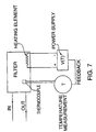
- FIG. 7 The requirements for a thermally tuned filter with closed loop temperature control are shown in Figure 7.
- the temperature is measured with a thermocouple; as the temperature varies from its setpoint (determined by the filtered wavelength desired) the power from the power supply to a resistive heating element is altered to maintain the desired setpoint temperature.
- the ambient temperature of the filter will be raised to a level 5 to 10°C beyond the expected environmental variation in temperature.
- An additional advantage of certain polymer Bragg grating filters is their low optical loss and low birefringence.
- a four channel tunable demultiplexer based on polymer waveguide gratings is used as defined in Figure 5.
- the channel spacing of the demultiplexer is 400 GHz or 3.2 nm.
- the specific wavelengths filtered when the device is held at 60°C are 1547.72, 1550.92, 1554.12, and 1557.32 nm.
- the four output fibers are terminated with FC/PC connectors.
- Two subsequent demultiplexers held at temperatures 68°C and 72°C filter wavelengths 1549.32, 1552.52, 1555.72 and 1559.96, and 1550.12, 1553.32, 1556.52, and 1560.72 nm, respectively.
- Interchannel crosstalk for the filtered channels is ⁇ -30 dB.
- the cumulative loss of light experienced at the final throughport for nonfiltered wavelengths is on the order of 15-20 dB.
- a four channel tunable demultiplexer based on polymer waveguide gratings is used as defined in Figure 6.
- the channel spacing of the demultiplexer is 100 GHz or 0.8 nm.
- the specific wavelengths filtered are 1547.72, 1548.52, 1549.32 and 1550.12 nm when the device is held at 60°C.
- the light from the fiber is launched into a GRIN lens provided by NGK that collimates the light from the fiber. This light is then incident on a thin filter interference filter made by OCLI that reflects at greater than 95% wavelengths from 1547.5 to 1550.3 nm.
- the light reflected is directed at another GRIN lens that focuses the light back down into the input fiber of the demultiplexer which then separates out the four wavelengths.
- Light not reflected by the first thin film interference filter passes to the next one, F 2 , which reflects wavelengths from 1550.5 to 1553.5 nm with greater than 95% efficiency.
- Thin film interference filters F 3 and F 4 act similarly, reflecting wavelength bands 1553.5 to 1556.7 and 1557.0 to 1560.2 nm, respectively.
- the derivative, d ⁇ B /d ⁇ is related to the photoelastic constants of the material, which depend on the refractive indices, the Poisson ratio, and generalized Pockel's coefficients, in general.
Description
Claims (8)
- A tunable integrated wavelength division multiplexer/demultiplexer optical signal device comprising at least two filter elements (2A, 2B, 40, 50, 60, 70, 80, 90), each of said filter elements being made of a material having an adjustable parameter, at least two of said filter elements being cascaded, and means (8A, 8B, 44, 54) for maintaining said adjustable parameter at different values for adjacent filter elements, wherein the filter elements are Mach-Zehnder interferometers integrated with tunable Bragg gratings (42,52).
- The tunable optical signal device of claim 1 wherein the adjustable parameter is selected from temperature and mechanical stress.
- The tunable optical signal device of claim 1 wherein the material is a thermosensitive material.
- The tunable optical signal device of claim 3 wherein the thermosensitive material is at least one thermosensitive polymer.
- The tunable optical signal device of claim 1 wherein the adjustable parameter is temperature, said means for maintaining the adjustable parameter comprising:a) a thermocouple for measuring the temperature of the material;b) a temperature sensor for comparing the temperature of the material to a preset temperature; andc) a heater for applying heat to the material to maintain said preset temperature.
- The tunable optical signal device of claim 1 further comprising a plurality of narrow band mirrors, each mirror segregating a set of plurality of wavelength signals and directing said set of wavelength signals to said filter elements.
- The tunable optical signal device of claim 1 further comprising GRIN lenses for collimating said set of wavelength signals before said set of wavelength signals enter the filter element.
- A method of dropping/adding at least one preselected wavelength of light from/to an optical signal comprising a set of wavelength signals, the method comprising passing said optical signal through a tunable optical signal device comprising at least two filter elements, the filter elements being Mach-Zehnder interferometers integrated with tunable Bragg gratings, each of said filter elements being made of a material having an adjustable parameter, and means for maintaining said adjustable parameter at different values for adjacent filter elements, said method comprising directing said set of wavelength signals to said filter elements and adjusting the parameter of at least one of said filter elements to reflect said at least one preselected wavelength of light.
Applications Claiming Priority (5)
| Application Number | Priority Date | Filing Date | Title |
|---|---|---|---|
| US7551298P | 1998-02-20 | 1998-02-20 | |
| US75512P | 1998-02-20 | ||
| US09/251,893 US6256428B1 (en) | 1999-02-19 | 1999-02-19 | Cascading of tunable optical filter elements |
| US251893 | 1999-02-19 | ||
| PCT/US1999/003853 WO1999042875A1 (en) | 1998-02-20 | 1999-02-22 | Cascading of tunable optical filter elements |
Publications (2)
| Publication Number | Publication Date |
|---|---|
| EP1055143A1 EP1055143A1 (en) | 2000-11-29 |
| EP1055143B1 true EP1055143B1 (en) | 2003-12-17 |
Family
ID=26756953
Family Applications (1)
| Application Number | Title | Priority Date | Filing Date |
|---|---|---|---|
| EP99934345A Expired - Lifetime EP1055143B1 (en) | 1998-02-20 | 1999-02-22 | Cascading of tunable optical filter elements |
Country Status (7)
| Country | Link |
|---|---|
| EP (1) | EP1055143B1 (en) |
| JP (1) | JP2002504706A (en) |
| CN (1) | CN1291294A (en) |
| AU (1) | AU3307599A (en) |
| CA (1) | CA2320083A1 (en) |
| DE (1) | DE69913657T2 (en) |
| WO (1) | WO1999042875A1 (en) |
Families Citing this family (16)
| Publication number | Priority date | Publication date | Assignee | Title |
|---|---|---|---|---|
| GB2344657A (en) * | 1998-11-06 | 2000-06-14 | Univ Heriot Watt | Wavelength selective optical filter |
| US6256431B1 (en) * | 1999-02-11 | 2001-07-03 | Eci Telecom Ltd. | WDM multiplexer |
| US6559988B1 (en) * | 1999-12-16 | 2003-05-06 | Lucent Technologies Inc. | Optical wavelength add/drop multiplexer for dual signal transmission rates |
| JP2001221041A (en) * | 2000-02-07 | 2001-08-17 | Sanshin Ind Co Ltd | Muffler mounting structure of outboard motor |
| JP3651876B2 (en) | 2000-02-07 | 2005-05-25 | エヌティティエレクトロニクス株式会社 | Wavelength multiplexed optical signal multiplexing / demultiplexing method |
| FR2823563B1 (en) * | 2001-04-12 | 2003-09-26 | Get Enst | QUICKLY TUNABLE MONO OR MULTI-FREQUENCY OPTICAL FILTER |
| US6816636B2 (en) * | 2001-09-12 | 2004-11-09 | Honeywell International Inc. | Tunable optical filter |
| US7145165B2 (en) | 2001-09-12 | 2006-12-05 | Honeywell International Inc. | Tunable laser fluid sensor |
| FI20022249A (en) * | 2002-12-20 | 2004-06-21 | Chun Ye | Tuners, tunable polarization-interference filters, and tuning methods |
| US7656532B2 (en) | 2006-04-18 | 2010-02-02 | Honeywell International Inc. | Cavity ring-down spectrometer having mirror isolation |
| US8009983B2 (en) * | 2008-06-26 | 2011-08-30 | Tyco Electronics Subsea Communications Llc | High loss loop back for long repeater span |
| US8198590B2 (en) | 2008-10-30 | 2012-06-12 | Honeywell International Inc. | High reflectance terahertz mirror and related method |
| US7864326B2 (en) | 2008-10-30 | 2011-01-04 | Honeywell International Inc. | Compact gas sensor using high reflectance terahertz mirror and related system and method |
| CN102033053B (en) | 2010-11-12 | 2012-06-20 | 浙江理工大学 | Method and device for measuring refractive index of air based on laser synthetic wavelength interferometry |
| CN102087371A (en) * | 2010-12-10 | 2011-06-08 | 福州高意通讯有限公司 | Optical slice heating method and tunable FP (Fabry-Perot) filter |
| CN103399419A (en) * | 2013-08-07 | 2013-11-20 | 苏州扬清芯片科技有限公司 | Temperature controlling type optical filtering device |
Family Cites Families (7)
| Publication number | Priority date | Publication date | Assignee | Title |
|---|---|---|---|---|
| US4632517A (en) * | 1983-12-08 | 1986-12-30 | University Of Pittsburgh | Crystalline colloidal narrow band radiation filter |
| JPS61151603A (en) * | 1984-12-26 | 1986-07-10 | Mitsubishi Electric Corp | Optical circuit parts |
| JP2741540B2 (en) * | 1989-07-10 | 1998-04-22 | キヤノン株式会社 | Color image forming equipment |
| US5671307A (en) * | 1995-04-10 | 1997-09-23 | Universite Laval | Use of a temperature gradient to impose a chirp on a fibre bragg grating |
| US6285810B1 (en) * | 1996-07-26 | 2001-09-04 | Italtel Spa | Tunable add/drop optical device |
| US5857043A (en) * | 1996-08-12 | 1999-01-05 | Corning Incorporated | Variable period amplitude grating mask and method for use |
| US5706375A (en) * | 1996-09-10 | 1998-01-06 | Jds Fitel Inc. | Variable-attenuation tunable optical router |
-
1999
- 1999-02-22 EP EP99934345A patent/EP1055143B1/en not_active Expired - Lifetime
- 1999-02-22 WO PCT/US1999/003853 patent/WO1999042875A1/en active IP Right Grant
- 1999-02-22 DE DE69913657T patent/DE69913657T2/en not_active Expired - Fee Related
- 1999-02-22 JP JP2000532755A patent/JP2002504706A/en not_active Withdrawn
- 1999-02-22 CA CA002320083A patent/CA2320083A1/en not_active Abandoned
- 1999-02-22 CN CN99803088A patent/CN1291294A/en active Pending
- 1999-02-22 AU AU33075/99A patent/AU3307599A/en not_active Abandoned
Also Published As
| Publication number | Publication date |
|---|---|
| AU3307599A (en) | 1999-09-06 |
| JP2002504706A (en) | 2002-02-12 |
| CN1291294A (en) | 2001-04-11 |
| WO1999042875A1 (en) | 1999-08-26 |
| DE69913657T2 (en) | 2004-10-07 |
| CA2320083A1 (en) | 1999-08-26 |
| DE69913657D1 (en) | 2004-01-29 |
| EP1055143A1 (en) | 2000-11-29 |
Similar Documents
| Publication | Publication Date | Title |
|---|---|---|
| US6256428B1 (en) | Cascading of tunable optical filter elements | |
| EP1055143B1 (en) | Cascading of tunable optical filter elements | |
| EP1508208B1 (en) | Closed-loop control of tunable optical wavelength filters | |
| JP4631089B2 (en) | Tunable etching diffraction grating for WDM optical communication system | |
| EP0903616A2 (en) | Switchable optical filter | |
| EP1243962A2 (en) | Wavelength tunable reflector and methods | |
| US6738543B1 (en) | Hitless tunable wavelength filters | |
| US20030190121A1 (en) | Athermal tunable filter with wavelength and intensity responses based on volume phase hologram | |
| US7010198B2 (en) | Birefringence trimming of integrated optical devices by elevated heating | |
| US6853759B2 (en) | Method and apparatus for sensing a temperature along an optical path with a grating in semiconductor material | |
| US20060002653A1 (en) | Apparatus for an optical circuit having a flat wavelength response | |
| US7072546B2 (en) | Compensation for chromatic dispersion | |
| US6546167B1 (en) | Tunable grating optical device | |
| Offrein et al. | Wavelength tunable 1-from-16 and flat passband 1-from-8 add-drop filters | |
| EP1652327B1 (en) | An electro-optically tunable optical filter | |
| US20030198438A1 (en) | Tunable add/drop multiplexer | |
| US6721100B2 (en) | Sandwiched thin film optical filter | |
| US20040071427A1 (en) | Waveguide-grating-based wavelength-intelligent devices | |
| EP0975998B1 (en) | Polymeric phased array | |
| WO2003079069A2 (en) | Optical filter array and method of use | |
| Eldada | Optical communication subsystems using microphotonic integrated circuits based on nanoengineered materials | |
| WO1998039676A1 (en) | Polymeric phased array | |
| JP2000111840A (en) | Polarizing beam splitter and optical communication method |
Legal Events
| Date | Code | Title | Description |
|---|---|---|---|
| PUAI | Public reference made under article 153(3) epc to a published international application that has entered the european phase |
Free format text: ORIGINAL CODE: 0009012 |
|
| 17P | Request for examination filed |
Effective date: 20000914 |
|
| AK | Designated contracting states |
Kind code of ref document: A1 Designated state(s): DE FR GB IT |
|
| GRAP | Despatch of communication of intention to grant a patent |
Free format text: ORIGINAL CODE: EPIDOSNIGR1 |
|
| GRAS | Grant fee paid |
Free format text: ORIGINAL CODE: EPIDOSNIGR3 |
|
| GRAA | (expected) grant |
Free format text: ORIGINAL CODE: 0009210 |
|
| AK | Designated contracting states |
Kind code of ref document: B1 Designated state(s): DE FR GB IT |
|
| PG25 | Lapsed in a contracting state [announced via postgrant information from national office to epo] |
Ref country code: IT Free format text: LAPSE BECAUSE OF FAILURE TO SUBMIT A TRANSLATION OF THE DESCRIPTION OR TO PAY THE FEE WITHIN THE PRESCRIBED TIME-LIMIT;WARNING: LAPSES OF ITALIAN PATENTS WITH EFFECTIVE DATE BEFORE 2007 MAY HAVE OCCURRED AT ANY TIME BEFORE 2007. THE CORRECT EFFECTIVE DATE MAY BE DIFFERENT FROM THE ONE RECORDED. Effective date: 20031217 |
|
| REG | Reference to a national code |
Ref country code: GB Ref legal event code: FG4D |
|
| REF | Corresponds to: |
Ref document number: 69913657 Country of ref document: DE Date of ref document: 20040129 Kind code of ref document: P |
|
| RAP2 | Party data changed (patent owner data changed or rights of a patent transferred) |
Owner name: E.I. DU PONT DE NEMOURS AND COMPANY |
|
| ET | Fr: translation filed | ||
| PLBE | No opposition filed within time limit |
Free format text: ORIGINAL CODE: 0009261 |
|
| STAA | Information on the status of an ep patent application or granted ep patent |
Free format text: STATUS: NO OPPOSITION FILED WITHIN TIME LIMIT |
|
| 26N | No opposition filed |
Effective date: 20040920 |
|
| PGFP | Annual fee paid to national office [announced via postgrant information from national office to epo] |
Ref country code: FR Payment date: 20050208 Year of fee payment: 7 |
|
| PGFP | Annual fee paid to national office [announced via postgrant information from national office to epo] |
Ref country code: GB Payment date: 20050216 Year of fee payment: 7 |
|
| PGFP | Annual fee paid to national office [announced via postgrant information from national office to epo] |
Ref country code: DE Payment date: 20050217 Year of fee payment: 7 |
|
| REG | Reference to a national code |
Ref country code: GB Ref legal event code: 732E |
|
| REG | Reference to a national code |
Ref country code: FR Ref legal event code: TP |
|
| PG25 | Lapsed in a contracting state [announced via postgrant information from national office to epo] |
Ref country code: GB Free format text: LAPSE BECAUSE OF NON-PAYMENT OF DUE FEES Effective date: 20060222 |
|
| PG25 | Lapsed in a contracting state [announced via postgrant information from national office to epo] |
Ref country code: DE Free format text: LAPSE BECAUSE OF NON-PAYMENT OF DUE FEES Effective date: 20060901 |
|
| GBPC | Gb: european patent ceased through non-payment of renewal fee |
Effective date: 20060222 |
|
| REG | Reference to a national code |
Ref country code: FR Ref legal event code: ST Effective date: 20061031 |
|
| PG25 | Lapsed in a contracting state [announced via postgrant information from national office to epo] |
Ref country code: FR Free format text: LAPSE BECAUSE OF NON-PAYMENT OF DUE FEES Effective date: 20060228 |