JP4622115B2 - Signal component separation device, filter device, reception device, communication device, and communication method - Google Patents
Signal component separation device, filter device, reception device, communication device, and communication method Download PDFInfo
- Publication number
- JP4622115B2 JP4622115B2 JP2001036727A JP2001036727A JP4622115B2 JP 4622115 B2 JP4622115 B2 JP 4622115B2 JP 2001036727 A JP2001036727 A JP 2001036727A JP 2001036727 A JP2001036727 A JP 2001036727A JP 4622115 B2 JP4622115 B2 JP 4622115B2
- Authority
- JP
- Japan
- Prior art keywords
- signal
- symbol
- group
- circuit
- output
- Prior art date
- Legal status (The legal status is an assumption and is not a legal conclusion. Google has not performed a legal analysis and makes no representation as to the accuracy of the status listed.)
- Expired - Fee Related
Links
Images


Description
【0001】
【発明の属する技術分野】
本発明は通信装置(通信システム)、送信機および受信機、並びに、通信方法に関するものであり、特に、マルチキャリア変調を行うディジタル通信装置(システム)、ディジタル通信装置(システム)に用いる無線送信機(無線送信装置)無線受信機(無線受信装置)、並びに、その通信方法に関する。
より特定的には、本発明は直交周波数分割多重化(OFDM:Orthogonal Frequency Division Multiplexing)方式で多重化されたマルチキャリア信号をシンボル系列に分離する信号成分分離装置、マルチキャリア信号から特定のシンボルを抽出するフィルタ装置、および、これら信号成分分離装置、フィルタ装置などを有する信号受信装置に関する。
【0002】
【従来の技術】
OFDM方式による変調信号の例としてDAB(Digital Audio Broadcasting、ディジタル・オーディオ放送) システムを例示する。
EUREKA147プロジェクトが開発した移動受信可能な高品質ディジタル音声地上放送方式としてDABシステムが知られている。DABシステムを衛星放送に適用したディジタル衛星音声放送も実用化が進められている。
【0003】
そのようなディジタル通信システム(装置)に使用される変調方式としては、マルチパスフェージング、ゴーストなどに強いという特徴を有するOFDM方式が提案されている。
OFDM方式は通常、直交する数十〜数百の搬送波を使用するマルチキャリア変調方式であり、各搬送波をQAM、PSKなどの変調方式で変調する。
DABシステムなどにおいては、マルチキャリア通信を適用して多重チャネルのディジタル音声信号を伝送する。
【0004】
図21(A)、(B)はマルチキャリア変調方式として、DABシステムなどに適用されるOFDM方式を用いたディジタル無線通信システムの一構成例を示す図である。図21(A)、(B)はDABシステムの一部を簡略化して図解している。
以下の説明では、DABシステムを例示して、多重化に関する部分を中心に説明を行う。
【0005】
図21(A)に図解したOFDM方式の無線通信システムの無線送信装置10は、符号化回路11と、シンボルマッピング回路12と、マルチプレクサ(信号多重化処理回路)13と、周波数インターリーブ回路14と、逆高速フーリエ変換(IFFT:Inverse Fast Fourier Transform) 回路15と、無線送信回路16と、アンテナ17とを有する。
【0006】
情報ビットストリームは、符号化回路11において符号化ならびにインターリーブなどの処理がなされた後に、シンボルマッピング回路12において各ビットが送信シンボルにマッピングされる。この作業はチャネル毎に各々別個に行われ、図21(A)に示した例においては、たとえば、チャネルあたり毎秒64ksps(シンボル/秒)のシンボルが生成されている。
【0007】
これらのシンボルストリームは、マルチプレクサ13において単純に直列に連結されることにより多重化されたシンボルストリームとなる。たとえば、64kspsのチャネルを18チャネル分多重すると、多重されたシンボルストリームの伝送レートは1152ksps(=18x64ksps)となる。
この多重されたシンボルストリームは周波数インターリーブ回路14における周波数インターリーブ処理によりシンボルの並び替えが行われる。この作業により各チャネルのシンボルはばらばらに並ぶことになる。
【0008】
その後、シンボルストリームは逆高速フーリエ変換(IFFT)回路15におけるIFFT処理によりばらばらに並ぶシンボルが周波数軸上にならべられ、これらの周波数軸上でのシンボル表現が時間軸上のシンボルに変換されて送信回路16からアンテナ17を介して空中に送出される。
【0009】
送信装置10から出力される6キャリアにマルチキャリア化されたシンボル列の例を図22に図解する。
【0010】
これまで、上述したマルチキャリア化された複数のシンボル(シンボル系列)の特定のシンボルのみを抽出することは行われていなかった。
そこで、無線信号受信機において、図22に例示したシンボル系列から所望のシンボルまたはキャリア成分を抽出する方法を既存の技術を用いて行う場合を想定する。
【0011】
図23はマルチキャリア信号を分離する第1の方法を示す図である。
この方法は、それぞれ対応するキャリアの周波数帯域特性を有する帯域フィルタを複数設けて、それぞれの帯域通過フィルタで対応するシンボルを抽出する。そのようなフィルタとしては、たとえば、くし型フィルタを用いることができる。
【0012】
しかしながら、このような方法は、OFDMのようにキャリアの間隔が詰まっている変調方式のシンボルの分離には不向きである。すなわち、OFDM方式による変調方式ではある周波数帯域に多数のキャリアが詰まっているので、隣接する信号成分のアイソレーションが十分にとれないので、隣接する周波数のキャリア信号を識別するには各帯域通過フィルタは急峻な周波数特性を持たねばならない。
【0013】
たとえば、くし型フィルタでそのような急峻な周波数特性を持つ精度の高いフィルタを各種準備することは困難であるし、価格などの面で相当高価格になるので、実現することが困難である。
【0014】
図24はマルチキャリア信号を分離する第2の方法を示す図である。
図24において、受信回路22で受信した信号を高速フーリエ変換(FFT)回路23で高速フーリエ変換を行い周波数軸上に並んだ受信シンボル系列を生成し、デマルチプレクサ(信号分離装置)29においてシンボル系列をばらばらのシンボルに分離して、特定のシンボルのみ選択可能にする。
しかしながら、この方法は、特定のシンボルを抽出する場合でも、全てのシンボルについて高速フーリエ変換を行うから、複雑なFFT回路23を設けなければならず、装置構成が複雑になる。
【0015】
図25は一定間隔のキャリア信号成分のみ抽出する場合の概略構成図である。図25において、複数の異なる通過帯域特性を有する複数の帯域通過フィルタを設けて、フィルタにより帯域制限した信号同士を加算回路28A、28Bで加算して所望の信号を得る。この場合も、帯域フィルタとして、たとえば、くし型フィルタを用いる。
しかしながら、この方法も、図23の方法と同様、マルチキャリア方式なのでキャリアが詰まっていて信号成分のアイソレーションが十分にとれない、および、急峻な周波数特性を持つ精度の高いフィルタを準備することが価格などの面で困難になるという問題に遭遇する。
【0016】
図21(B)は、図21(A)に図解したDABシステムにおける無線信号受信機の概略構成図である。
図21(B)のOFDM方式の無線通信システム1の無線受信装置20は、アンテナ21と、受信回路22と、高速フーリエ変換(FFT)回路23と、シンボル選択回路24と、ビット抽出回路25と、復号回路26とを有する。
【0017】
受信回路22でアンテナ21で受信した所望の周波数帯域の信号を周波数変換してベースバンド信号成分のみを抽出することにより、ベースバンド信号を得る。このようにして得られたベースバンド信号は、情報が周波数軸上に並んでいる信号の時間軸上での表現となっているので、FFT回路23においてFFT処理して周波数軸上に並んでいるサブキャリアを抽出する。
このとき、FFT処理によって出力されるシンボルは受信した信号帯域全体のサブキャリア群となる(たとえば、本例においては1152ksps分の情報が含まれている)。
【0018】
シンボル選択回路24は、サブキャリア群の中から、図21(A)に図解した送信側で行われた周波数インターリーブにより配置された所望のチャネルのシンボルの存在位置からシンボルを抽出する。これにより所望のチャネルの情報である64kbpsが抽出されたことになる。
【0019】
ビット抽出回路25においてこのようにして得られた所望のチャネルのシンボルストリームから受信ビットストリームを抽出して符号化ビットストリームを得た後、復号回路26においてこれをデコードすることにより、所望のチャネルの情報ビットストリームを得ている。
【0020】
【発明が解決しようとする課題】
このように、OFDMのシステムにおいては、サブキャリア毎に異なるチャネルのシンボルを割り当てることにより多重化が行われているが、無線受信装置20は、送信されてきた全チャネル分の多重化信号を全て受信し、さらにはFFT回路23により全チャネル分のシンボルを抽出した後にシンボル選択回路24においてチャネルの選定を行っており、本来必要であった1チャネル分の情報に必要とされる演算量を上回る演算がFFT回路23においてFFT処理が行われていることになる。
すなわち、無線受信装置20が欲していないチャネルの分をも含めてFFT回路23においてFFT信号処理を行っていることになり、FFT回路23の回路規模が大きくなるという問題がある。
【0021】
上述した問題を解決する方法として、本願の発明者は、たとえば、平成11年5月20日に出願した、特願平11−140442号に記載された発明を提案している。特願平11−140442号に記載された発明はシンボル系列から交互のサブキャリアごとシンボル列を分離する回路を二分岐方式で多段に階層的に設けている。
【0022】
本発明は、特願平11−140442号に記載された発明とは異なる方法で上記問題を解決するとともに、さらに、1シンボルのみを効率よく抽出することを目的とする。
【0023】
本発明の目的は、シンボル系列を効率よく二分岐的に分離可能な信号成分分離装置を提供することにある。
【0024】
本発明の他の目的は、シンボル系列から特定のシンボルを効率よく抽出可能なフィルタ装置を提供することにある。
【0025】
本発明のさらに他の目的は、上記信号成分分離装置および/またはフィルタ回路を有する受信装置を提供することにある。
【0026】
本発明のさらに他の目的は、上記受信装置と送信装置とを有する通信システムを提供することにある。
【0027】
本発明の他の目的は、上記受信処理と上記送信処理を行う通信方法を提供することにある。
【0028】
【課題を解決するための手段】
本発明の第1の観点によれば、マルチキャリア変調された信号群(シンボル群)からある信号群を分離する信号成分分離装置であって、
入力信号群をN/2(m+1) シンボル遅延するシンボル遅延手段と、
入力信号群を0Hzを基準として−π(k/2m )ラジアン位相シフトする位相オフセット調整手段と、
上記シンボル遅延手段の出力信号と上記位相オフセット調整手段の出力信号を加算して上記信号選択出力手段に入力された多重化信号のうち周波数軸上交互に位置する一方のシンボル列を算出する加算手段と、
上記シンボル遅延手段の出力信号から上記位相オフセット調整手段の出力信号を減算して上記信号選択出力手段に入力された多重化信号のうち周波数軸上交互に位置する他方のシンボル列を算出する減算手段と
からなる二分岐回路が二分岐方式で段階的かつ階層的に接続されている、信号成分分離装置が提供される。
ただし、mは二分岐回路の段数の位置を示すパラメータであり、
Nは1変調時間内に存在するシンボルの数であり、
kは0(Hz)を基準としてサブキャリアの周波数オフセット
を持つ信号群が入力されていることを示すパラメータである。
【0029】
本発明の第2の観点によれば、上記信号成分分離装置を適用した、複数チャネルのサブキャリアが周期的に配置されているマルチキャリア変調による多重通信に用いる受信装置が提供される。
当該受信装置は、
信号群を受信する受信手段と、
入力した信号群をN/2(m+1) シンボル遅延するシンボル遅延手段と、入力した信号群を−π(k/2m )ラジアン位相シフトする位相オフセット調整手段と、上記シンボル遅延手段の出力信号と上記位相オフセット調整手段の出力信号を加算して上記信号選択出力手段に入力された多重化信号のうち周波数軸上交互に位置する一方のシンボル列を算出する加算手段と、上記シンボル遅延手段の出力信号から上記位相オフセット調整手段の出力信号を減算して上記信号選択出力手段に入力された多重化信号のうち周波数軸上交互に位置する他方のシンボル列を算出する減算手段と、からなる二分岐回路が二分岐方式で段階的かつ階層的に接続されている、信号成分分離装置と、
上記信号成分分離装置で分離した信号群について直交変換を行う直交変換手段と、
上記直交変換した情報を復号する復号手段と
を具備する。
【0030】
本発明の第3の観点によれば、上記受信装置を適用した、複数チャネルのサブキャリアが周期的に配置されているマルチキャリア変調による多重通信に用いる、送信装置と受信装置とを有する、通信装置が提供される。
当該通信装置の上記送信装置は、複数チャネルの情報を独立に符号化する符号化手段と、上記符号化した情報をそれぞれ所定の変調方式に基づいて変調して信号点配置を行う信号点配置手段と、上記複数の信号点配置した信号を時間周期的に多重化する信号多重化手段と、上記多重化した信号を逆直交変換する逆直交変換手段と、上記直交変換した情報を送出する送信手段と、を有する。
当該通信装置の上記受信装置は、上述した受信装置の構成要素、すなわち、上記送出された信号群を受信する受信手段と、上記受信した信号群を選択分離する信号成分分離手段と、上記選択分離された信号を直交変換する直交変換手段と、上記直交変換した情報を復号する復号手段とを有する。
上記信号成分分離手段は、上述した構成を有する。
【0031】
好ましくは、上記送信装置における上記信号多重化手段は、上記複数の信号点配置した信号を所定のサブキャリアでチャネルごと周波数をずらして多重化する。
【0032】
また好ましくは、上記送信装置における上記信号点配置手段における変調方式は直交周波数多重化方式(OFDM方式)を用いる変調方式である。
【0033】
また好ましくは、上記送信装置における上記逆直交変換処理手段は逆フーリエ変換処理を行い、上記受信機における上記直交変換処理手段はフーリエ変換処理を行う。
【0034】
本発明の第4の観点によれば、複数チャネルのサブキャリアが周期的に配置されているマルチキャリア変調による多重通信に用いる受信装置であって、
信号群を受信する受信手段と、
入力信号群をN/2(m+1) 遅延するシンボル遅延手段と、入力信号群を−π(k/2m )ラジアン位相シフトする位相オフセット調整手段と、上記シンボル遅延手段の出力信号と上記位相オフセット調整手段の出力信号を加算して上記信号選択出力手段に入力された多重化信号のうち周波数軸上交互に位置する一方のシンボル列を算出する加算手段と、上記シンボル遅延手段の出力信号から上記位相オフセット調整手段の出力信号を減算して上記信号選択出力手段に入力された多重化信号のうち周波数軸上交互に位置する他方のシンボル列を算出する減算手段と、からなる二分岐回路が二分岐方式で段階的かつ階層的に接続されている信号成分分離装置と、
上記信号成分分離装置で分離したシンボル列のうち、所定のサブキャリアのシンボル群を1系列または複数系列選択して出力する信号選択手段と、
上記信号選択手段で選択出力した1系列または複数系列のシンボル群について周波数オフセット補償する周波数オフセット補償手段と、
上記周波数オフセット補償手段のそれぞれの出力信号について直交変換を行う2つの直交変換手段と、
上記直交変換した信号を復号する復号手段と
を具備する受信装置が提供される。
【0035】
好ましくは、上記周波数オフセット補償手段は、上記周波数オフセット補償のために複素正弦波信号を出力する周波数オフセット補償信号発生手段と、上記信号群と、上記周波数オフセット補償信号発生手段から出力される複素正弦波信号とを乗算する乗算手段と、該乗算手段における乗算結果のシンボルを周波数軸に沿って並べ替えるシンボル並べ替え手段とを有する。
【0036】
本発明の第5の観点によれば、第4の観点の受信装置を用いた、複数チャネルのサブキャリアが周期的に配置されているマルチキャリア変調による多重通信に用いる、送信装置と受信装置とを有する通信装置が提供される。
【0037】
本発明の第6の観点によれば、複数チャネルのサブキャリアが周期的に配置されているマルチキャリア変調による多重通信に用いる受信装置であって、
信号群を受信する受信手段と、
入力信号群をN/2(m+1) 遅延するシンボル遅延手段と、入力信号群を−π(k/2m )ラジアン位相シフトする位相オフセット調整手段と、上記シンボル遅延手段の出力信号と上記位相オフセット調整手段の出力信号を加算して上記信号選択出力手段に入力された多重化信号のうち周波数軸上交互に位置する一方のシンボル列を算出する加算手段と、上記シンボル遅延手段の出力信号から上記位相オフセット調整手段の出力信号を減算して上記信号選択出力手段に入力された多重化信号のうち周波数軸上交互に位置する他方のシンボル列を算出する減算手段と、からなる二分岐回路が二分岐方式で段階的かつ階層的に接続されている信号成分分離装置と、
上記信号成分分離手段で分離した1系列または複数系列のシンボル群について周波数オフセット補償する周波数オフセット補償手段と、
上記周波数オフセット補償手段のそれぞれの出力信号について直交変換を行う2つの直交変換手段と、
上記直交変換した信号を復号する復号手段と
を具備する受信装置が提供される。
【0038】
本発明の第7の観点によれば、上記受信装置を適用した、複数チャネルのサブキャリアが周期的に配置されているマルチキャリア変調による多重通信に用いる、送信装置と受信装置とを有する通信装置が提供される。
【0039】
本発明の第8の観点によれば、マルチキャリア変調された信号群から特定の信号を抽出するフィルタ装置であって、
入力信号群をN/2(m+1) 遅延するシンボル遅延手段と、入力信号群を−π(k/2m )ラジアン位相シフトする位相オフセット調整手段と、上記シンボル遅延手段の出力信号と上記位相オフセット調整手段の出力信号を加算して上記信号選択出力手段に入力された多重化信号のうち周波数軸上交互に位置する一方のシンボル列を算出する加算手段と、上記シンボル遅延手段の出力信号から上記位相オフセット調整手段の出力信号を減算して上記信号選択出力手段に入力された多重化信号のうち周波数軸上交互に位置する他方のシンボル列を算出する減算手段と、からなる二分岐回路が二分岐方式で段階的かつ階層的に接続されている信号成分分離装置と、
上記信号成分分離装置で分離したシンボル列のうち、特定のサブキャリアのシンボル群を選択して出力する信号選択手段と、
上記信号選択手段で選択出力したシンボル群について周波数オフセット補償する周波数オフセット補償手段と
を具備するフィルタ装置が提供される。
【0040】
本発明の第9の観点によれば、上記フィルタ装置を適用した、複数チャネルのサブキャリアが周期的に配置されているマルチキャリア変調による多重通信に用いる受信装置であって、
マルチキャリア変調された信号群を受信する受信手段と、
上記受信手段で受信したマルチキャリア変調された信号群から特定の信号を抽出するフィルタ装置と、
該フィルタ装置で抽出した信号について直交変換を行う直交変換手段と、
上記直交変換した信号を復号する復号手段と
を具備する受信装置が提供される。
【0041】
本発明の第10の観点によれば、マルチキャリア変調された信号群から特定の信号を抽出するフィルタ装置であって、
サブキャリアを選択するサブキャリア選択手段と、
上記選択されたサブキャリアに応じて、入力された信号群から特定の信号群を選択して出力する、少なくとも1段の信号選択手段と、
上記信号選択手段で選択した信号について周波数オフセット補償する周波数オフセット補償手段と
を具備する、フィルタ装置が提供される。
【0042】
本発明の第11の観点によれば、上記フィルタ装置を適用した、複数チャネルのサブキャリアが周期的に配置されているマルチキャリア変調による多重通信に用いる受信装置であって、
マルチキャリア変調された信号群を受信する受信手段と、
上記受信手段で受信したマルチキャリア変調された信号群から特定の信号を抽出するフィルタ装置と、
該フィルタ装置で抽出した信号について直交変換を行う直交変換手段と、
上記直交変換した信号を復号する復号手段と
を具備する受信装置が提供される。
【0043】
本発明の第12の観点によれば、マルチキャリア変調された信号群から特定の信号を抽出するフィルタ装置であって、
選択すべきチャネルに応じた複素正弦波信号を出力する通過サブキャリア選択信号出力手段と、
上記通過サブキャリア選択出力手段から出力された複素正弦波信号と、入力信号群との乗算を行う乗算手段と、
上記乗算手段における乗算結果のうち、特定の信号群を選択する少なくとも1段の信号成分分離手段と、
上記信号成分分離装置の出力を周波数軸上に並べ替えるシンボル並べ替え手段と
を具備するフィルタ装置が提供される。
【0044】
本発明の第13の観点によれば、上記フィルタ装置を適用した、複数チャネルのサブキャリアが周期的に配置されているマルチキャリア変調による多重通信に用いる受信装置であって、
マルチキャリア変調された信号群を受信する受信手段と、
上記受信手段で受信したマルチキャリア変調された信号群から特定の信号を抽出するフィルタ装置と、
該フィルタ装置で抽出した信号について直交変換を行う直交変換手段と、
上記直交変換した信号を復号する復号手段と
を具備する受信装置が提供される。
【0045】
本発明の第14の観点によれば、複数チャネルのサブキャリアが周期的に配置されているマルチキャリア変調による多重通信に用いる受信装置であって、
マルチキャリア変調された信号群を受信する受信手段と、
入力信号群をスイッチングするスイッチング手段と、
上記受信手段で受信したマルチキャリア変調された信号群を保持するバッファ手段と、
上記スイッチング手段の後段に接続され、入力された信号群のうち特定の信号群を選択出力するフィルタ装置と、
上記フィルタ装置で抽出した信号について直交変換を行う直交変換手段と、
上記直交変換した信号を復号する復号手段と
を具備し、
上記スイッチング手段は1シンボル分の信号群を上記フィルタ装置に出力し、上記バッファ手段はその間、入力された1シンボル分の信号群を保持し、上記フィルタ装置への信号送出終了後、上記バッファ手段に保持した信号群を上記スイッチング手段を介して上記フィルタ装置に送出し、
上記フィルタ装置は、上記スイッチング手段を介して入力された信号群のうち指定されたサブキャリアのみ選択出力する、
受信装置が提供される。
【0046】
上記フィルタ装置は、上述した各種のフィルタ装置を適用できる。
【0047】
本発明の第15の観点によれば、複数チャネルのサブキャリアが周期的に配置されているマルチキャリア変調による多重通信に用いる受信装置であって、
マルチキャリア変調された信号群を受信する受信手段と、
上記受信手段で受信したマルチキャリア変調された信号群のうち偶数キャリアの信号群を選択して出力する第1のフィルタ装置と、
上記受信手段で受信したマルチキャリア変調された信号群のうち奇数キャリアの信号群を選択して出力する第2のフィルタ装置と、
上記第2のフィルタ装置の出力信号群を保持するバッファ手段と、
上記第1のフィルタ装置の出力信号群をスイッチングするスイッチング手段と、
上記スイッチング手段の後段に接続され、スイッチングされた出力信号について直交変換を行う直交変換手段と、
上記直交変換した信号を復号する復号手段と
を具備し、
上記スイッチング手段は上記第1のフィルタ装置の出力信号を上記直交変換手段に送出し、上記直交変換手段への信号送出終了後、上記バッファ手段に保持した信号群を上記スイッチング手段を介して上記直交変換手段に送出する、
受信装置が提供される。
【0049】
本発明の第16の観点によれば、通信方法であって、
複数チャネルの情報を独立に符号化し、
上記符号化した情報をそれぞれ所定の変調方式に基づいて変調して信号点配置を行い、
上記複数の信号点配置した信号を時間周期的に多重化し、
上記多重化した信号を逆直交変換し、
上記直交変換した情報を送出する
符号化送信工程と、
上記送出された信号を受信し、
上記受信した直交変換処理後の多重化信号のうち、希望するチャネルの信号のみ選択出力し、
上記選択出力された信号を直交変換し、
上記直交変換した情報を復号する
受信復号工程と
を有する通信方法であって、
上記受信工程における信号選択処理は、
N/2(m+1) シンボル遅延し、
π(k/2m )ラジアンだけ位相シフトし、
上記シンボル遅延した信号と上記位相シフトした信号を加算して上記入力された多重化信号のうち周波数軸上交互に位置する一方のシンボル列を算出するか、上記シンボル遅延した信号から上記位相シフトした信号を減算して上記入力された多重化信号のうち周波数軸上交互に位置する他方のシンボル列を算出する
方法を二分岐的かつ段階的に行う
通信方法が提供される。
【0050】
【発明の実施の形態】
本発明の通信装置(通信システム)、送信装置(送信機)および受信装置(受信機)、並びに、通信方法について、添付図面を参照して好適実施の形態を述べる。
【0051】
下記の実施の形態においては、通信システムとして無線通信システムについて例示するが、本発明は無線通信システムに限定されず、有線通信システムにも適用できる。しかしながら下記の実施の形態においては、無線通信システム、たとえば、DABシステムに類似する直交周波数分割多重化(OFDM)方式を用いて通信システムについて例示する。
【0052】
通信装置の第1実施の形態
図1(A)、(B)、図2(A)、(B)、(C)、および、図3を参照して本発明の通信システム、送信装置、受信装置、並びに、通信方法の第1実施の形態を述べる。
【0053】
図1(A)、(B)は本発明の通信システム、送信装置および受信装置、並びに、通信方法の1実施の形態としてのマルチキャリア変調方式としてOFDM方式を用いたディジタル無線通信システムの構成図であり、図1(A)はOFDM方式の無線通信システムの送信装置30の構成図であり、図1(B)はOFDM方式の無線通信システムの受信装置40の構成図である。
【0054】
送信装置30と受信装置40とで、OFDM方式の無線通信システムを構成している。
【0055】
送信装置(送信機)30
送信装置(送信機)30について述べる。
図1(A)に図解したOFDM方式の無線通信システムの送信装置30は、第1チャネル用符号化回路311 および第1チャネル用シンボルマッピング回路321 、第2チャネル用符号化回路312 および第2チャネル用シンボルマッピング回路322 、〜、第Mチャネル用符号化回路31M および第Mチャネル用シンボルマッピング回路32M を有する。この例は、Mチャネルの情報ビットストリームを符号化する例を示す。
送信装置30はさらに、マルチプレクサ(信号多重化処理回路)34と、スクランブル処理・IFFT・ガードタイム付加・窓かけ処理回路36と、送信回路38と、アンテナ39とを有する。
【0056】
送信装置30は、このように、複数の符号化回路311 〜31M と複数のシンボルマッピング回路321 〜32M に対して、1系統のマルチプレクサ34、スクランブル処理・IFFT・ガードタイム付加・窓かけ処理回路36、送信回路38を有している。符号化回路31およびシンボルマッピング回路32はチャネル数だけ設けられる。
【0057】
チャネル1〜チャネルMのそれぞれ独立した情報ビットストリームについて、符号化回路311 〜31M においてそれぞれ独立して符号化、インターリーブ等の処理が行われる。
【0058】
符号化回路311 〜31M における符号化処理の具体例を述べる。OFDM方式の無線通信システムがたとえばDABシステムのようなオ−ディオ信号の伝送に適用される場合、情報ビットストリームのビット信号はオーディオ信号であるから、符号化回路311 〜31M はそれぞれオーディオ信号について符号化処理を行う。符号化回路311 〜31M は必要に応じて、さらにインターリーブ処理をも行う。
【0059】
符号化回路311 〜31M において生成された各チャネルの符号化ビット信号はシンボルマッピング回路321 〜32M において、送信シンボルにマッピングされ、シンボルストリームが生成される。
【0060】
シンボルマッピング回路321 〜32M においては、OFDM方式に適用する各種の変調方式を適用することができる。そのような変調方式としては、多値QAM、PSKなど各種の変調方式が適用できる。
このようにシンボルマッピング回路321 〜32M において、図2(A)に図解したように、各チャネルで各々独立したシンボルストリームが生成される。
【0061】
複数チャネルごとのシンボルストリームはマルチプレクサ34において多重化され、多重シンボルストリームとして生成される。マルチプレクサ34は、図2(B)に図解したスイッチ回路を有しており、マルチプレクサ34の多重化処理によって、図2(A)に図解した複数チャネルのシンボルが図2(C)に図解したように周波数軸上に複数のチャネルのシンボルが並んだ多重化シンボルストリームとなる。
【0062】
マルチプレクサ34において多重化された多重化シンボルストリームは、スクランブル処理・IFFT・ガードタイム付加・窓かけ処理回路36において、ランダム位相シフト処理(RPS:Randam Phase Shift)、ランダム直交変換処理(ROT:Randam Orthogonal Transform)等などによりスクランブルされる。
【0063】
スクランブル処理・IFFT・ガードタイム付加・窓かけ処理回路36において逆フーリエ変換処理(IFFT処理)によって周波数ドメイン多重化シンボルストリームから時間ドメインの多重化シンボルストリームに変換される。
さらにスクランブル処理・IFFT・ガードタイム付加・窓かけ処理回路36においてガードタイムの付加ならびに窓かけ処理(ウインドー処理)が施される。
【0064】
スクランブル処理・IFFT・ガードタイム付加・窓かけ処理回路36は、後述するスクランブル処理、逆高速フーリエ変換(IFFT:Inverse Fast Fourier Transform) 処理、ガードタイム処理、窓かけ処理(ウインドー処理)などを総称して1つの手段として示したものであり、これらの処理を個別の回路または個別の手段に分離して処理してもよい。
【0065】
スクランブル処理・IFFT・ガードタイム付加・窓かけ処理回路36における、スクランブル処理、ガードタイム付加・窓かけ処理は本発明にとって必須ではない。しかしながら、スクランブル処理を行うと、通信の秘匿性(機密性)が高まる。
【0066】
直交変換の代表例として、IFFTを例示したが、スクランブル処理・IFFT・ガードタイム付加・窓かけ処理回路36におけるIFFTに代えて、他の直交変換処理、たとえば、逆離散コサイン変換(IDCT:Inverse Discrete Cosine Transform )処理を行うこともできる。
【0067】
以上から、スクランブル処理・IFFT・ガードタイム付加・窓かけ処理回路36は基本的には、直交変換処理を行う回路または手段である。
【0068】
スクランブル処理・IFFT・ガードタイム付加・窓かけ処理回路36の出力シンボルは、送信回路38において高周波信号と畳込まれ所望の周波数帯域に周波数変換された後、アンテナ39を介して空中に送信される。
【0069】
図2(A)〜(C)を参照してマルチプレクサ34の内部の構成ならびにこの多重化方法により生成される各チャネルのシンボルの並びについて説明する。
図2(A)〜(C)は、図1に図解したマルチプレクサ34における多重送信の基本概念を示す図である。
図1(A)に図解したマルチプレクサ34は基本的に、図2(B)に図解したスイッチング回路として構成されている。
【0070】
図2(A)は、マルチプレクサ34において多重化された各チャネルのシンボルストリームを示している。ここでは、チャネル1(CH1)からチャネル4(CH4)まで4つのチャネルについて例示している。それぞれのチャネルのシンボルストリームは個別にマルチプレクサ34に挿入されている。
【0071】
図2(B)はマルチプレクサ34における処理の概念を示したものである。入力されてきた各チャネルのシンボルストリームをサイクリックにスイッチング処理して、各チャネルのシンボルが周期的に現れるようにシンボルを配置する。多重化されたシンボルストリームを図2(C)に示す。
【0072】
この例示は、最大4チャネルの多重化を行う場合を例にとったため各チャネルのシンボルの出現周期は4であるが、最大のチャネル多重数はこれに限定されることはなく、任意の整数nに関して2n (n=1、2、3、4、…)に設定することができる。その場合の各チャネルのシンボルの出現周期は、最大の多重数と同じ2n となる。
【0073】
マルチプレクサ34における多重化処理を22 チャネルの処理とした場合、実際に通信に用いられるチャネル数が最大の多重数よりも小さい場合には、使われていないチャネルのシンボルとして振幅が「0(ゼロ)」のヌル(Null)シンボルを挿入して、マルチプレクサ34における周期的な多重化処理を行う。
【0074】
図3は複数チャネルのサブキャリアの並びを示す図である。
図3に図解した例示においては、チャネル数が4で、サブキャリア間隔が隣接するチャネルごと4kHzのOFDM処理を行っている場合、すなわち1シンボル変調時間が250μs=1/4kHzである場合を例示している。多重信号のサブキャリア間隔は4kHzであるが、チャネル1〜チャネル4は1サブキャリア単位で周波数軸上に周期的に出現するため、各チャネルのサブキャリアは、16kHz=4×4kHzおきに出現している。
図3における記号fc はキャリア(搬送波)周波数(帯域信号の中心周波数)を示す。
【0075】
本発明の実施の形態においては、マルチキャリア変調による多重通信を行うときに、複数チャネルのサブキャリアが周期的に配置されるようにしている。その理由は、多数のシンボルの変調を容易にするためであり、さらに後述する受信装置40におけるチャネル選択回路43においてチャネル分離を容易にするためである。
【0076】
受信装置の第1実施の形態
図1(B)に図解したOFDM方式の無線通信システムの受信装置40について述べる。
この実施の形態において、送信装置30と同様、多重チャネル数が4でサブキャリア間隔が4kHzのOFDM処理を行っている場合、すなわち1シンボル変調時間が250μs=1/4kHzである場合を例示する。さらに、説明の都合上、多重信号の信号帯域が1024kHzで、サブキャリアが256本存在する場合を例示する。これは、1チャネルあたりのサブキャリア数が64本(=256本/4)の多重である場合に相当する。
【0077】
受信装置40は、受信アンテナ41と、高周波受信回路42と、信号成分分離装置(デマルチプレクサ、または、チャネル選択回路)43と、FFT・デスクランブル処理手段44と、ビット抽出回路45と、復号回路46とを有する。
【0078】
OFDM方式の無線通信システムの送信装置30より送信された信号は、受信アンテナ41で受信され、高周波受信回路42においてベースバンド帯域にダウンコンバートされる。さらに、図解しないA/D変換器においてディジタル信号に変換されて、接続線202より信号成分分離装置43に入力される。
【0079】
信号成分分離装置43には、チャネル1〜チャネル4までの信号が周波数軸上に並べられている信号が時間軸上での表現で入力されることになる。
信号成分分離装置43は、送信装置30におけるマルチプレクサ34の処理とは逆に、複数のチャネルごとに信号を分離する(デマルチプレクシングする)。この信号成分分離装置43の詳細な回路構成と処理方法については、図4〜図7を参照して後述する。
【0080】
高周波受信回路42から信号成分分離装置43に入力されるシンボル数は、1変調時間あたり256個であるが、(簡単のためここではオーバーサンプルは考えない)、所望のチャネルのサブキャリア本数はその1/4であるから、チャネル選択回路43では周波数軸上でのデシメーション(decimation)が行われ、64個(=256個/4)のシンボルが出力される。これにより、FFT・デスクランブル処理手段44におけるFFT処理のシンボル数が1/4に減少する。
【0081】
信号成分分離装置43の出力シンボルが信号線204を介してFFT・デスクランブル処理手段44に入力される。
FFT・デスクランブル処理手段44において、送信装置30におけるスクランブル処理・IFFT・ガードタイム付加・窓かけ処理回路36で行ったIFFT(逆高速フーリエ変換)とは逆の高速フーリエ変換(FFT)処理が行われ、周波数軸上に並んでいるシンボル列が抽出される。
【0082】
信号成分分離装置43において所望のチャネルのシンボルが選択されて抽出されてFFT・デスクランブル処理手段44に印加されているから、FFT処理により抽出されたシンボルは、所望のチャネル以外の他のチャネルのシンボルは含まれていない。すなわち、処理手段44における処理は所望のチャネルを受信するのに必要最低限のポイント数をもつFFT処理で充分である。その結果、FFT・デスクランブル処理手段44におけるFFT処理回路が小規模になる。
【0083】
このようにして抽出された所望のチャネルのシンボルストリームは、スクランブル処理・IFFT・ガードタイム付加・窓かけ処理回路36におけるランダム位相シフト処理、ランダム直交変換処理等などの処理に対応する処理を行い、送信装置30において行われたスクランブルを解いた後、信号線206を介してビット抽出回路45に入力される。
【0084】
ビット抽出回路45において、シンボルが変調されている変調方式に応じてビットを抽出し、符号化ビットストリームを復号回路46へ印加する。そのような変調方式としては、OFDM方式において適用されるQPSK、8PSK、16QAMなど様々な変調方式を適用できる。
【0085】
復号回路46は、送信装置30における複数チャネルの符号化回路311 〜31M で行われた符号化やインターリーブとは逆のデインターリーブおよび復号処理を行うことにより、情報ビットストリームを抽出する。
【0086】
多数のサブキャリアのシンボル列の信号を受信した受信装置40に信号成分分離装置43を設けることにより、FFT・デスクランブル処理手段44、ビット抽出回路45、復号回路46におけるサンプルレートを所望のチャネル分に低下させて(デシメーションして)から行うことが可能となり、FFT・デスクランブル処理手段44以降の回路45〜46の処理量を大幅に、たとえば、(1/多重数分)に低減することが可能となる。
【0087】
特に、信号成分分離装置43をFFT・デスクランブル処理手段44の前段に設けてFFT・デスクランブル処理手段44におけるFFT処理のデータ数を減少させているので、FFT処理のためのメモリ容量が少なくなり、受信装置40の小規模化に大きく貢献する。また、FFT・デスクランブル処理手段44におけるFFT処理時間を短縮できる。
【0088】
各チャネルのサブキャリアは、システムの周波数帯域全体にまたがって配置されることから、本実施の形態をDABシステムのような多数のチャネルが多重化されている無線通信システムに適用した場合、大きな周波数ダイバーシティ効果が期待できる。これにより、フェーディングによる通信品質の劣化を抑えることが可能となる。
【0089】
信号成分分離装置43
図4〜図7を参照して、図1(B)に示した信号成分分離装置43の実施の形態について述べる。
図4は信号成分分離装置43の構成図である。
図5は図4に図解した信号成分分離装置43を構成する二分岐回路の回路図である。
図6は図5に図解したシンボル遅延回路43aの態様を示す図である。
図7は図5に図解した位相オフセット調整回路43bの態様を示す図である。
本実施の形態においては、サブキャリアが23 チャネル=8チャネルC0〜C7の場合について述べる。
【0090】
図4に図解した信号成分分離装置43は、1個の第1段目の二分岐回路431と、2個の第2段目の二分岐回路4321 、4322 と、4個の第3段目の二分岐回路4331 〜4334 を有する。信号成分分離装置43のこの回路構成は、シンボルを順次、二分岐する二分岐回路431:4321 、4322 :4331〜4334 が2の巾乗の形態で拡散するように(または、2の巾乗の形態でピラミッドのように階層的に)構成されている。
【0091】
二分岐回路の意味は、シンボル列が入力されたとき、サブキャリアごと交互に2系統に分岐したシンボル列を抽出するからである。
【0092】
信号成分分離装置43は、図4に図解したように、個別の二分岐回路431、4321 、4322 、および、4331 〜4334 を組み合わせて構成することができるし、これらの二分岐回路を1個のDSP(デジタル信号プロセッサ)で構成することもできる。以下、個別に二分岐回路を設けて、それを組み合わせた場合について述べる。
【0093】
図4における記号の意味を説明する。
記号Nは高周波受信回路42から出力され、信号成分分離装置43で受信したシンボル系列の1変調時間あたりのサンプルポイント数を示す。
記号K(大文字)は信号成分分離装置43の内部の各段の二分岐回路において分離するシンボルの分離数を示す。第1段の二分岐回路431は2系列のシンボル列に分離するからK=2であり、第2段の2つの二分岐回路4321 、4322 で4系列のシンボル列に分離するからK=4であり、第3段の4つの二分岐回路4331 〜4334 で8系列のシンボル列に分離するからK=8である。
記号mは二分岐回路の段の位置を示す。第1段をm=0とする。
記号k(小文字)はその二分岐回路に0(Hz)を基準としていくつのサブキャリア分の周波数オフセットを持つ信号群が入力されていることを示すパラメータである。
【0094】
二分岐回路はそれぞれ、パラメータ(m,k)を用いて表すことができる。その具体的な意味については図5を参照して述べる。
【0095】
信号成分分離装置43は、高周波受信回路42から出力されたベースバンド帯域のマルチキャリア・ディジタル信号(マルチキャリア多重信号)をサブキャリア単位に分離する。
高周波受信回路42で受信したシンボル列は周期的に配列されているから、信号成分分離装置43は受信信号を2C キャリアおきの2c 個に分離する。cは任意の整数であり、2c =2,4,8,16,・・・・となる。
【0096】
図5は図4に図解した二分岐回路の一般的な回路構成を示す。
二分岐回路は、シンボル遅延回路43aと、位相オフセット調整回路43bと、加算回路43cと、減算回路43dとで構成される。
【0097】
m段のシンボル遅延回路43aは、そのシンボル遅延回路43aに入力されるシンボルの数のメモリ容量を有し、入力されたシンボル系列をシンボル個数N/(2(m+1) )だけ遅延する。段数mは、第1段の段数m=0とする。シンボル遅延回路43aは、実質的には1変調時間内のNシンボルについて、(2(m+1) )シンボルを遅延する。
シンボル遅延回路43aは、たとえば、FIFO(First-In First-Out) メモリ、通常のランダムアクセスメモリなどで構成できる。
【0098】
図6にm=0〜m=3についてのシンボル遅延回路43aの遅延量を図解する。
【0099】
図5に図解した第1段の二分岐回路431に、高周波受信回路42から8チャネルC0〜C7のシンボル系列が入力された場合、m=0、2(m+1) =2であるから、第1段の二分岐回路431のシンボル遅延回路43aはシンボル数Nの半分だけ遅延する。
【0100】
同様に、第2段の二分岐回路4321 ,4322 におけるシンボル遅延回路43aは、第1段の二分岐回路431のシンボル遅延回路43aの半分のメモリ容量を有し、シンボル数N/4だけ遅延する。
第3段の二分岐回路4321 〜4324 におけるシンボル遅延回路43aは第1段の二分岐回路431のシンボル遅延回路43aの1/4のメモリ容量を有し、シンボル数N/8だけ遅延する。
【0101】
各段の二分岐回路において、出力されるシンボルの数が入力されたシンボルの数の半数となることから、デシメーションが行われたことと等価になり、後段の二分岐回路に入力されるシンボル数は前段の二分岐回路に入力されるシンボル数の半分になり、シンボル遅延回路43aのメモリ容量も、後段にいくにしたがい、前段の半分になる。
【0102】
m段の位相オフセット調整回路43bは、−π(k/(2m )(ラジアン)だけ、入力されたシンボルの位相をずらす(位相オフセットする)。
図3に図解したように、サブキャリア群により0(Hz)を基準として周波数オフセットがあるので、位相オフセット調整回路43bは、このオフセットにより発生する位相の回転を調整するための位相シフトを行う。その位相シフト量は、0(Hz)を基準としてサブキャリア分の周波数オフセットを示すk(小文字)と段数mとに応じた量の角度、−π(k/2m )(ラジアン)である。
【0103】
図7に各種パラメータm,kについての位相オフセット調整回路43bの位相シフト状態を図解する。
【0104】
第1段の二分岐回路431における位相オフセット調整回路43bは、パラメータがm=0、k(小文字)=0であるから、位相の回転は行わない。
【0105】
第2段の二分岐回路4321 の位相オフセット調整回路43bは、パラメータがm=1,k=0であるから、第1段の二分岐回路431における位相オフセット調整回路43bと同様、位相回転を行わない。
しかし、第2段の二分岐回路4322 の位相オフセット調整回路43bは、パラメータがm=1,k(小文字)=1であるから、−π/2(ラジアン)だけ位相を回転する。この位相回転は、図解のごとく、I軸とQ軸とを入れ換えて、かつ、極性を反転することを意味する。シンボルの位相の回転は、π/2の倍数のときは信号の極性の逆転、または、I軸とQ軸との入れ換えを行うだけでよい。
【0106】
第3段の二分岐回路4331 〜4334 のそれぞれの位相オフセット調整回路43bは、パラメータ、m=2,k(小文字)=1〜3について、図解のごとく、位相シフトを行う。k=0の場合は位相シフトを行わない。
【0107】
このように、二分岐回路における位相オフセット調整回路43bによる位相シフトは、極性の反転、加減算、係数乗算によって実現できる。
【0108】
図5に図解した二分岐回路の動作について述べる。
二分岐回路は入力された信号を交互に分離し、シンボル列を周波数軸上でデシメーションする回路である。
【0109】
図5に図解のごとく、8チャネルのサブキャリアC0,C1,C2,C3〜C7の信号列(サブキャリア群)が第1段の二分岐回路431に入力された場合、シンボル遅延回路43aにおいてシンボル数(N/2)だけ遅延したシンボルと、位相オフセット調整回路43bにおいて、k=0であり、位相シフトされていないシンボル列とを加算回路43cで加算すると、サブキャリアC0,C2,C4,C6のシンボル系列のみが分離して抽出される。
【0110】
減算回路43dにおいて、シンボル遅延回路43aにおいてシンボル数N/2だけ遅延したシンボルから位相オフセット調整回路43bにおいて位相シフトしていないシンボル列を減じるとサブキャリアC1,C3,C5,C7のシンボル系列のみが分離して抽出される。このように、第1段の二分岐回路431は入力された交互のサブキャリアごと、シンボル系列を分離する。
【0111】
分離されたシンボル系列は、それぞれ周波数軸上の分解能が半分にデシメーションされており、出力されるシンボル数は両出力ともN/2シンボルになる。
【0112】
第2段の二分岐回路4321 にサブキャリアC0,C2,C4,C6が入力されると、シンボル遅延回路43aにおいてシンボル数N/4だけ遅延したシンボルと、位相オフセット調整回路43bにおいて、k=0であり位相回転されていないシンボル列とを加算回路43cで加算すると、サブキャリアC0,C4のシンボル系列が抽出される。
二分岐回路4321 の減算回路43dにおいて、シンボル遅延回路43aにおいてN/4だけ遅延したシンボルから位相オフセット調整回路43bにおいて位相回転されていないシンボル列を減じると、サブキャリアC2,C6のシンボル系列が抽出される。
【0113】
このように、第2段の二分岐回路4311 においても入力されたサブキャリアを交互に分離してシンボル系列を出力する。分離されたシンボル系列はそれぞれ、周波数軸上の分解能が半分になっており、デシメーションされている。
【0114】
なお、第2段の二分岐回路4311 におけるシンボル遅延回路43aのメモリ容量は、第1段の二分岐回路431におけるシンボル遅延回路43aのメモリ容量の半分である。
【0115】
第2段の二分岐回路4322 にサブキャリアC1,C3,C5,C7が入力されると、シンボル遅延回路43aにおいてN/4(サンプリング時間)だけ遅延したシンボルと、位相オフセット調整回路43bにおいて、k=1,m=1であり、−π/2(ラジアン)だけ位相シフトされたシンボル列とを加算回路43cで加算するとサブキャリアC1,C5のシンボル系列が抽出される。
【0116】
二分岐回路4321 の減算回路43dにおいて、シンボル遅延回路43aにおいてN/4だけ遅延したシンボルから位相オフセット調整回路43bにおいて−π/2(ラジアン)だけ位相シフトされたシンボル列を減じるとサブキャリアC3,C7のシンボル系列が抽出される。
【0117】
このように、第2段の二分岐回路4312 においも、入力されたサブキャリアが交互に分離されたシンボル系列を抽出する。分離されたシンボル系列はそれぞれ、周波数軸上で分解能が半分になっており、デシメーションされている。
【0118】
なお、第2段の二分岐回路4312 におけるシンボル遅延回路43aのメモリ容量は、第1段の二分岐回路431におけるシンボル遅延回路43aのメモリ容量の半分である。
【0119】
第3段の二分岐回路4331 〜4334 においても、上記同様のシンボル分離とデシメーションを行う。
その結果、最終的には第3段の二分岐回路4331 〜4334 の各出力線から、チャネルC0,C4,C2,C6,C1,C5,C3,C7のシンボルが分離されて出力される。
【0120】
これら1サブキャリアごとのシンボルに分離されたシンボルは、たとえば、図8を参照して後述する周波数オフセット補償回路(周波数オフセット補償・除去手段)を通して周波数オフセットが補正された後に、図1(B)に図解したFFT・デスクランブル処理手段44に印加される。FFT・デスクランブル処理手段44以降の動作は前述した。
FFT・デスクランブル処理手段44には周波数軸上の分解能を落とした信号が印加されるから、FFT・デスクランブル処理手段44の回路構成は簡単になる。
【0121】
このように二分岐回路を階層的に組み合わせた構成した信号成分分離装置43によれば、各段で入力したサブキャリアごと交互にシンボルを交互に分離するとともに、周波数軸上における信号成分の分解能を順次1/2に低下させる(デシメーションする)ことができる。
【0122】
信号成分分離装置43の各部を構成している二分岐回路は、基本的に同じ回路構成をしており、第1段から段2段、第3段にいくに従い、シンボル遅延回路43aのメモリ容量が順次半分になっていくこと、および、位相オフセット調整回路43bにおける位相シフト量を異ならせる他は、基本的に同じ回路構成をしている。したがって、簡単な構成の二分岐回路を組み合わせて構成される信号成分分離装置43の構成も簡単である。さらに、デシメーションが1/(2の巾乗)単位で行われるから、多数のサブキャリアが変調されたマルチキャリアにおいても、回路構成が簡単になる。
【0123】
以上の実施の形態は8シンボル列について例示したが、8シンボル列、16シンボル列、32シンボル列などの分離が可能であることはどの分離も上記と同様の方法に従って実現できる。また、2シンボル列、4シンボル列への分離が可能であることは言うまでもない。
【0124】
受信装置の第2実施の形態
図8は本発明の第2実施の形態としての受信装置40Aの構成図である。
図8に図解した受信装置40Aは、図1(B)に図解した受信装置40と同様、図1(A)に図解した送信装置30から送出されたマルチキャリア信号を受信する。
【0125】
受信装置40Aは、信号成分分離装置43と、信号選択回路47と、2つの周波数オフセット補償回路48A、48Bを有する。
この実施の形態では、2つの周波数オフセット補償回路48A、48Bを設けた例を図解しているが、周波数オフセット補償回路は複数並列に設けることができる。
【0126】
周波数オフセット補償回路48A、48Bの後段には、図1(B)に図解した、FFT・デスクランブル処理手段44、ビット抽出回路45、復号回路46などが、周波数オフセット補償回路の個数に合わせた系統、本実施の形態では2系統、設けられる。
【0127】
信号成分分離装置43は、図4に図解したと同様の二分岐回路を階層化した構成をとることができる。したがって、信号成分分離装置43からはサブキャリア単位で信号成分を、2C 通りに(ただし、Cは任意の整数)、分離した信号成分が得られる。
【0128】
信号選択回路47は、信号成分分離装置43で分離した信号成分のうち希望するサブキャリアのシンボルを選択して出力する。図4の図解から明らかなように、信号成分分離装置43の最終段の二分岐回路の出力がどのサブキャリア群に対応するか一義的に決まっているので、信号選択回路47におけるシンボルの選択は容易である。この例では信号選択回路47は2つのシンボルを選択出力しているが、信号選択回路47における選択シンボル数は、1または任意の複数にすることができる。
【0129】
周波数オフセット補償回路48A、48Bは、信号選択回路47で選択したサブキャリア群の信号が、図3に図解したように周波数オフセットがあるので、それを補償する。
【0130】
図9は周波数オフセット補償回路48A、48Bの回路構成例を示す図である。
周波数オフセット補償回路48A、48Bはそれぞれ、乗算器481と、ジャイレータ(オシレータ)482と、シンボル並べ替え回路483とを有する。
【0131】
乗算器481に入力される信号は、0(Hz)を基準として、下記に示すプラス方向に異なる周波数オフセットを有している。
【0132】
【数1】
exp(j2π(k/N)i+πk)
【0133】
このオフセットを除去するため、ジャイレータ482は、下記に示す上記オフセットと共役の複素正弦波の信号を乗算器481に出力する。このように、ジャイレータ482は、下記の複素成分信号を発生する信号発生装置である。
【0134】
【数2】
exp(−j2π(k/N)i+πk)
【0135】
乗算器481は信号選択回路47で選択されたシンボルと、ジャイレータ482からの上記複素正弦波信号との乗算を行い、周波数変換してオフセット成分を除去する。
【0136】
シンボル並べ替え回路483は周波数変換した結果のうち、前半部分と後半部分を入れ替えて、その結果を出力する。
【0137】
本実施の形態において、図1(B)のFFT・デスクランブル処理手段44におけるFFT処理の前に、複数、本実施の形態では2つの処理対象とするシンボル数の削減が行われているので、FFT回路の構成が簡単になり、処理速度が向上する。
【0138】
すなわち、本実施の形態によれば、FFT・デスクランブル処理手段で扱うシンボル数は上述した図1(B)の半分となる。
シンボル数をNで表すと、FFT回路を構成しているゲート数は、(logN)に比例したゲート数となる。したがって、FFT回路に入力されるシンボル数が少なくなると、FFT回路のゲート数は極端に減少する。
図1(B)のFFT・デスクランブル処理手段44におけるFFTのゲート数と、図8に図解した受信装置におけるFFT・デスクランブル処理手段の2つのFFT回路のゲート数の和を比較すると、本実施の形態のFFT・デスクランブル処理手段の2つのFFT回路のゲート数の和のほうが小さくなる。このことは、2つのFFT・デスクランブル処理手段を設けたほうが、図1(B)に図解の1つのFFT・デスクランブル処理手段44より回路構成が簡単になることを意味する。さらに構成の簡単なFFT回路は動作速度を高めることができる。したがって、図8の受信装置40Aを用いると、全体の回路構成が簡単になり、動作速度も向上するという利点がある。
【0139】
なお、信号選択回路47におけるサブキャリア群の選択は2つに限らず、1サブキャリア群だけでもよいし、2以上の複数のサブキャリア群を選択することもできる。
【0140】
受信装置の第3実施の形態
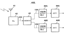
図10は本発明の第3実施の形態としての受信装置40Bの構成図である。
図10に図解した受信装置40Bは、図1(B)に図解した受信装置40と同様、または、図8に図解した受信装置40Aと同様、図1(A)に図解した送信装置30から送出されたマルチキャリア信号を受信する。
【0141】
受信装置40Bは、高周波受信回路42と、信号成分分離装置43と、2系列の周波数オフセット補償回路48A、48Bとを有する。
この実施の形態では、2つの周波数オフセット補償回路48A、48Bを設けた例を図解しているが、周波数オフセット補償回路は複数並列に設けることができる。
【0142】
周波数オフセット補償回路48A、48Bの後段には、図1(B)に図解した、FFT・デスクランブル処理手段44、ビット抽出回路45、復号回路46などが、周波数オフセット補償回路の個数に合わせた系統、本実施の形態では2系統、設けられる。
【0143】
信号成分分離装置43には、たとえば、図4に図解した第1段の二分岐回路431と、第2段の二分岐回路4321 と、第3段目の二分岐回路4331 、4332 を設ける。その結果、信号成分分離装置43からはC0,C4,C2,C6のサブキャリア群と、C1,C5,C3,C7のサブキャリア群とが分離される。
【0144】
周波数オフセット補償回路48A、48Bは、信号成分分離装置43で分離したサブキャリア群の信号が、図3に図解したように周波数オフセットがあるので、それを補償する。
周波数オフセット補償回路48A、48Bは、第2実施の形態において述べた。すなわち、周波数オフセット補償回路48A、48Bの回路構成例を図9に図解し、その動作は上述したので、説明を省略する。
【0145】
FFT・デスクランブル処理手段44A、44Bはそれぞれ、周波数オフセット補償回路48A、48Bで周波数オフセット補償された、C0,C4,C2,C6のサブキャリア群、C1,C5,C3,C7のサブキャリア群についてFFT処理などを行う。
【0146】
FFT・デスクランブル処理手段44A、44Bで扱うシンボル数は上述した図1(B)の半分となる。シンボル数をNで表すと、FFT回路を構成しているゲート数は、(logN)に比例したゲート数となる。したがって、FFT回路に入力されるシンボル数が少なくなると、FFT回路のゲート数は極端に減少する。図1(B)のFFT・デスクランブル処理手段44におけるFFTのゲート数と、図10に図解したFFT・デスクランブル処理手段44A、44Bの2つのFFT回路のゲート数の和を比較すると、FFT・デスクランブル処理手段44A、44Bの2つのFFT回路のゲート数の和のほうが小さくなる。このことは、2つのFFT・デスクランブル処理手段44A、44Bを設けたほうが、図1(B)に図解の1つのFFT・デスクランブル処理手段44より回路構成が簡単になることを意味する。さらに構成の簡単なFFT回路は動作速度を高めることができる。
したがって、図10の受信装置40Bを用いると、全体の回路構成が簡単になり、動作速度も向上するという利点がある。
【0147】
以上の例示は、周波数オフセット補償回路、および、FFT・デスクランブル処理手段44A、44Bを2系統設ける場合について述べたが、これらを2の巾乗の数だけ並列に設けることができる。
【0148】
受信装置の第4実施の形態
図11は本発明の第4実施の形態の受信装置40Cの概略構成図である。
受信装置40Cも、上述した第1〜第3実施の形態の受信装置40、40A、40Bと同様、図1(A)の送信装置30から送出されたマルチキャリア信号を分離して復号する。
【0149】
受信装置40Cは、受信アンテナ41、高周波受信回路42、フィルタ装置49、FFT・デスクランブル処理手段44を有する。
FFT・デスクランブル処理手段44以降の回路は、図1(B)と同様である。
【0150】
図11に図解した受信装置40Cと上述した受信装置40、40A、40Bとの相違を述べると、受信装置40Cは受信装置40、40A、40Bのように信号成分分離装置43を用いて複数のシンボル系列を抽出するのではなく、フィルタ装置49により所望の1つのサブキャリア群の信号成分のみを抽出して、その結果を、FFT・デスクランブル処理手段44以降の回路で処理する。
【0151】
高周波受信回路42は上述したように、受信アンテナ41アンテナで受信した高周波信号をベースバンド帯域に周波数変換を行い、ベースバンド帯域に周波数変換したアナログ信号からディジタル信号(9シンボル列)に変換する。
【0152】
フィルタ装置49は、高周波受信回路42からのディジタル・シンボル列を入力してサブキャリア単位でフィルタして、所望のサブキャリア群のみ抽出する。フィルタ装置49は、出力されるサブキャリア群を表現するのに最低必要なサンプル数しか出力しない。その結果、周波数軸上の大幅なデシメーションが実現される。
【0153】
信号成分分離装置(二分岐回路)とフィルタ装置との相違を述べる。信号成分分離装置は、1信号群を入力して、1信号群を分離した2信号群を出力する。これに対して、フィルタ装置は、1信号群を入力して、特定の周波数帯域の1信号群を選択して出力する。
【0154】
FFT・デスクランブル処理手段44以降の回路は、図1(B)の受信装置40などの回路を参照して述べたと同様の処理を行う。
【0155】
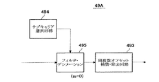
フィルタ装置の第1実施の形態
図12は図11に示したフィルタ装置の第1の実施の形態の回路例である。
図12に図解したフィルタ装置49は、信号成分分離装置(デマルチプレクサ)491と、シンボル群選択回路492と、周波数オフセット補償回路(周波数オフセット補償・除去回路)493とで構成されている。
【0156】
フィルタ装置49の構成は、図8の回路構成、すなわち、信号成分分離装置43、信号選択回路47、周波数オフセット補償・除去回路48A、48Bと類似しており、フィルタ装置49は実質的に図8のこれらの回路43、47、48A、48Bと同等の処理を行う。
【0157】
信号成分分離装置491は図8の信号成分分離装置43と同様、図4に図解した二分岐回路の組み合わせの回路構成である。
シンボル群選択回路492は図8の信号選択回路47と同様である。
周波数オフセット補償・除去回路493は図9に図解した周波数オフセット補償・除去回路48A、48Bと同様の回路構成である。
【0158】
信号成分分離装置491は、高周波受信回路42から出力されたシンボル列について所望のサブキャリア間隔でシンボルを分離する。
周波数オフセット補償・除去回路(周波数オフセット補償回路)493は、図9に図解した回路構成をしており、入力されたシンボル(信号)を基準を0(Hz)としてサブキャリア群に周波数変換を行い、周波数オフセット除去を行う。
【0159】
図11のFFT・デスクランブル処理手段44は選択されたシンボルについてのみFFT処理を行うので、DFTのポイント数を小さく抑えることができ、FFT・デスクランブル処理手段44の回路構成は簡単になる。
【0160】
フィルタ装置の第2実施の形態
図13は図11のフィルタ装置の第2の実施の形態の回路例である。
第2実施の形態のフィルタ装置は、受信したサブキャリア群を、奇数組のキャリアと偶数組のキャリアとに2分岐するフィルタ装置である。
第2実施の形態のフィルタ装置49Aは、サブキャリア選択回路494と、フィルタ・デシメーション回路495と、周波数オフセット補償・除去回路493とを有する。
【0161】
図14は図13に図解したフィルタ・デシメーション回路495の回路構成例を示す図である。
フィルタ・デシメーション回路495は、シンボル遅延回路495aと、位相オフセット調整回路495bと、加算回路495cとで構成されている。
【0162】
フィルタ・デシメーション回路495の回路構成は、図5に図解した信号成分分離装置43の1単位の二分岐回路に類似している。すなわち、シンボル遅延回路495aはシンボル遅延回路43aに対応し、位相オフセット調整回路495bは位相オフセット調整回路43bに対応し、加算回路495cは加算回路43cに対応している。ただし、フィルタ・デシメーション回路495には、減算回路43dは設けられていない。その理由は、フィルタ・デシメーション回路495においては、図5に図解した二分岐回路のように偶数サブキャリアと奇数サブキャリアの両者を必要とせず、いずれか一方のみの出力でよいからである。
【0163】
シンボル遅延回路495aは、入力されたサブキャリアC0〜C7を、パラメータN、mによって定められたポイント分、すなわち、N/(2m+1 )だけ、予め遅延する。本実施の形態においては、m=0であり、シンボル遅延回路495aの遅延はN/2となる。
【0164】
サブキャリア選択回路494が希望するサブキャリアを選択する。
位相オフセット調整回路495bは、入力されたサブキャリアC0〜C7に対して、サブキャリア選択回路494で選択した通過サブキャリア群に応じて位相シフトを行う。
【0165】
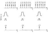
位相オフセット調整回路495bで行う回転位相の値(位相シフト量)は、−(α/2m )π(ラジアン)である。パラメータαは、通過させるサブキャリア群およびパラメータmによって決定される値であり、下記の表1に示す規則性をもっている。下記表において、C0〜C7は、0Hzから並んだサブキャリアを意味する。
【0166】
【表1】

フィルタ・デシメーション回路495を多段にすることにより、K(大文字)=8,16,32などのフィルタ装置を構成することができる。その場合、各々の段の位相オフセット調整回路495bで行われる回転位相の値は下記の表2に示す値となる。ただし、表2にはK=8までを例示した。
【0168】
【表2】
本実施の形態において、位相オフセット調整回路495bで行う回転位相の値は、偶数キャリアを通過させるときには0(rad)であり、奇数キャリアを通過させるときにはπ(rad)である。どちらの回転位相が適用されるかは、サブキャリア選択回路404により適宜指示される。
【0170】
加算回路495cは、位相オフセット調整回路495bで行った回転位相処理したサブキャリアと、シンボル遅延回路495aで遅延したサブキャリアとを加算する。
その結果、たとえば、フィルタ・デシメーション回路495に、サブキャリアC0〜C7が入力されたとき、フィルタ・デシメーション回路495からは、サブキャリア選択回路494で指定されたいずれか一方のサブキャリア系列のシンボルが出力される。
【0171】
図13のフィルタ装置49A内の周波数オフセット補償・除去回路493は、図12の周波数オフセット補償・除去回路493と同様、図9に図解したと同様の回路構成をしている。周波数オフセット補償・除去回路493は、上述した図8の周波数オフセット補償・除去回路48A、48B、または、図12の周波数オフセット補償・除去回路493と同様の動作を行う。
【0172】
図13に図解したフィルタ装置49Aにおいては、フィルタ・デシメーション回路495により周波数軸上でのデシメーションが行われ、出力シンボルの数が半分になる。したがって、それ以降の信号処理が、簡単で、迅速になる。
【0173】
フィルタ装置の第3実施の形態
図15は、図11に図解したフィルタ装置の第3の実施の形態の回路図である。
図15に図解したフィルタ装置49Bは、サブキャリア選択回路494と、第1のフィルタ・デシメーション回路495Aと、第2のフィルタ・デシメーション回路495Bと、周波数オフセット補償・除去回路493とを有する。
フィルタ装置49Bは、図13に図解したフィルタ装置49Aのフィルタ・デシメーション回路495を直列に設けられた2段のフィルタ・デシメーション回路495A、495Bに置き換えた回路である。フィルタ・デシメーション回路495A、495Bは共に、図14に図解した回路構成であり、第1段のフィルタ・デシメーション回路495Aはm=0であり、第2段のフィルタ・デシメーション回路495Bはm=1であり、このパラメータmを適用すると、図6に図解したように、それぞれのフィルタ・デシメーション回路495A,495Bにおける遅延量が規定される。
【0174】
周波数オフセット補償・除去回路493は図9に図解した回路と同様の回路構成をとることができる。
【0175】
位相オフセット調整回路495bで行う回転位相の値(位相シフト量)は、−(α/2m )π(ラジアン)である。パラメータαは、通過させるサブキャリア群およびパラメータmによって決定される値であり、表1に示す規則性をもっている。
【0176】
フィルタ・デシメーション回路495を多段にすることにより、K(大文字)=8,16,32などのフィルタ装置を構成することができる。その場合、各々の段の位相オフセット調整回路495bで行われる回転位相の値は表2に示す値となる。
本実施の形態において、位相オフセット調整回路495bで行う回転位相の値は、偶数キャリアを通過させるときには0(rad)であり、奇数キャリアを通過させるときにはπ(rad)である。どちらの回転位相が適用されるかは、サブキャリア選択回路404により適宜指示される。
【0177】
加算回路495cは、位相オフセット調整回路495bで行った回転位相処理したサブキャリアと、シンボル遅延回路495aで遅延したサブキャリアとを加算する。
その結果、たとえば、フィルタ・デシメーション回路495に、サブキャリアC0〜C7が入力されたとき、フィルタ・デシメーション回路495からは、サブキャリア選択回路494で指定されたいずれか一方のサブキャリア系列のシンボルが出力される。
【0178】
図15に図解したフィルタ装置49Bは、2段のフィルタ・デシメーション回路495A、495Bを設けているので、4つのサブキャリア群のいずれかを出力するフィルタ装置となる。すなわち、周波数軸上で1/4のデシメーションを行った信号を出力する回路である。
本実施の形態においては、2個のフィルタ・デシメーション回路495A、495Bを2段に直列連結した場合を例示したが、さらに3段、4段と多段(m)に連結し、23 、24 、2m のサブキャリア群に分離し、そのうちの1つのサブキャリア群を通過させることが可能となる。その場合、各フィルタ・デシメーション回路のパラメータmの規則性は図4と同様である。また、回転させる位相の値については、表1および表2に示した規則性による決定される。
【0179】
フィルタ装置の第4実施の形態
図16は、図11に図解したフィルタ装置の第4の実施の形態の回路例である。
フィルタ装置49Cは、乗算器496と、通過サブキャリア選択信号出力回路497と、フィルタ・デシメーション回路499と、シンボル並べ替え回路498とを有する。
【0180】
乗算器496に入力されるシンボル列の周波数オフセットは、図9の乗算器481に入力されるシンボル列の周波数オフセットと同じである。
【0181】
通過サブキャリア選択信号出力回路497は、その周波数オフセットを除去するため、図9に図解したジャイレータ(オシレータ)482と同様、選択すべきチャネルに応じた複素正弦波信号を乗算器496に出力する。
【0182】
乗算器496は、高周波受信回路42からのシンボル系列と通過サブキャリア選択信号出力回路497から出力された複素正弦波信号との乗算を行う。この演算は、フィルタ装置49Cに入力されたシンボル系列のうち、フィルタ装置49Cで選択するシンボル(サブキャリア成分)に0(Hz)が含まれるように周波数オフセットを持たせるためである。
したがって、通過サブキャリア選択信号出力回路497からは選択するサブキャリアのうち、0(Hz)から正周波数方向で最も近いサブキャリア分の周波数の信号と共役を出力し、乗算器496がその共役信号と入力されたシンボルとの乗算を行い、周波数オフセットを除去する。
【0183】
フィルタ・デシメーション回路499について、図17を参照して述べる。
図17は、図16に図解したフィルタ・デシメーション回路499の回路例である。
フィルタ・デシメーション回路499は、シンボル遅延回路495aと加算回路495cとで構成されている。
フィルタ・デシメーション回路499の回路構成は、図5に図解した二分岐回路から位相オフセット調整回路43bと減算回路43dを削除した回路構成であり、図14に図解したフィルタ・デシメーション回路495の回路構成から位相オフセット調整回路495bを削除した回路構成である。
フィルタ・デシメーション回路499は、入力されたサブキャリアのうち、0(Hz)を基準として偶数番目のサブキャリアのチャネルのシンボル系列のみを選択出力する回路である。
フィルタ・デシメーション回路499によっても、出力されるシンボル数が1/2となり、周波数軸上でデシメーションが行われたことになる。
【0184】
シンボル並べ替え回路498は、フィルタ・デシメーション回路499から出力されたシンボル群(サブキャリア群)の順序を、前半部分と後半部分とを入れ換えて、後半部分のシンボルのみを有効なシンボルとして出力する。
【0185】
フィルタ装置の第5実施の形態
図18は、図11に図解したフィルタ装置の第5の実施の形態の回路例である。
フィルタ装置49Dは、乗算器496と、チャネル選択信号出力回路497と、第1および第2のフィルタ・デシメーション回路499A、499Bと、シンボル並べ替え回路498とを有する。
第1および第2のフィルタ・デシメーション回路499A、499Bはそれぞれ、図17を参照して述べたフィルタ・デシメーション回路499と同様の回路構成をしている。
【0186】
フィルタ装置49Dは、図16に図解したフィルタ装置49Cに、第2のフィルタ・デシメーション回路499Bを追加したものである。フィルタ・デシメーション回路499Bの追加により、図15に図解した2段のフィルタ・デシメーション回路495A、495Bの回路構成と同様、図16に図解したフィルタ装置49Cより、さらに通過キャリアを1/2に制限することができる。
その他は、図16に図解したフィルタ装置49Cと同様である。
【0187】
なお、フィルタ・デシメーション回路499をさらに多段に直列接続することにより、たとえば、m段直列接続することにより、通過キャリアを1/2m に制限することができる。
【0188】
受信装置の第5実施の形態
図19は本発明の第5実施の形態の受信装置の構成図である。
受信装置40Dは、受信アンテナ41、高周波受信回路42、スイッチ回路50、バッファ回路52、フィルタ装置49、FFT・デスクランブル処理手段44、および、図解を省略した図1(B)に図解のビット抽出回路45、復号回路46を有する。
【0189】
高周波受信回路42は上記同様の動作を行う。
【0190】
スイッチ回路50は初期状態において、高周波受信回路42の信号をフィルタ装置49に出力する。
その間、バッファ回路52は、1シンボル分の信号が全てフィルタ装置49に転送されるまで、高周波受信回路42の信号を蓄積し続ける。
【0191】
フィルタ装置49は上述した各種の実施の形態として示したフィルタ装置49であり、高周波受信回路42からスイッチ回路50を通過して入力された信号のうちの指定された一部のサブキャリアのみ、たとえば、偶数キャリアのみの信号を抽出して、周波数軸上でのデシメーションを行い、その選択信号をFFT・デスクランブル処理手段44に出力する。
【0192】
FFT・デスクランブル処理手段44は、高周波受信回路42で受信したサブキャリア数より少ないサブキャリア数についてFFT処理を行う回路として構成されている。すなわち、FFT・デスクランブル処理手段44は小型、高速動作可能に構成されている。FFT・デスクランブル処理手段44でFFT処理などを行った後、図1(A)に図解したビット抽出回路45、復号回路46などにおける処理が行われる。
【0193】
バッファ回路52は、高周波受信回路42からの1シンボル分の信号が全てフィルタ装置49に転送された後、スイッチ回路50を経由してフィルタ装置49に信号の送出を開始する。
スイッチ回路50は高周波受信回路42の信号がフィルタ装置49に転送し終わると、バッファ回路52からの信号をフィルタ装置49に印加するように切り替わる。
フィルタ装置49は、先に通過させなかった信号成分のうち本通信において必要となる信号成分を通過させた信号、たとえば、奇数キャリアを抽出し、FFT・デスクランブル処理手段44に印加する。
FFT・デスクランブル処理手段44は、再度入力された信号をFFT処理して受信シンボルを抽出し、ビット抽出回路45以降の回路の処理を行わせる。
【0194】
図19に図解した回路構成をとることにより、高周波受信回路42において受信したシンボルをFFT処理するに本来必要なFFT回路より小規模の回路で、受信シンボルの抽出が可能となる。すなわち、図19の回路構成をとると、FFT・デスクランブル処理手段44の回路規模を小規模にすることができる。
【0195】
図19に図解した受信装置の回路構成は、受信シンボルを半分にした場合を例示したが、フィルタ装置49における通過キャリアをさらに減縮することにより、4分割、8分割などにすることができる。その結果、FFT・デスクランブル処理手段44の回路規模は一段と小型になる。
【0196】
受信装置の第6実施の形態
図20は本発明の第6実施の形態の受信装置の構成図である。
受信装置40Eは、受信アンテナ41、高周波受信回路42、第1のフィルタ装置49A、第2のフィルタ装置49B、スイッチ回路50、バッファ回路52、FFT・デスクランブル処理手段44、および、図解を省略した図1(B)に図解のビット抽出回路45、復号回路46を有する。
【0197】
高周波受信回路42は上記同様の動作を行う。
【0198】
フィルタ装置49A,49Bは、上述した各種のフィルタ装置49の回路構成をとることができ、第1のフィルタ装置49Aは、たとえば、偶数キャリアの信号の抽出を行い、第2のフィルタ装置49Bは、たとえば、奇数キャリアの信号の抽出を行う。すなわち、本実施の形態においては、フィルタ装置49A,49Bはそれぞれ、シンボルを1/2にデシメーションを行う。
【0199】
スイッチ回路50は初期状態において、フィルタ装置49Aから出力される偶数キャリアの信号をFFT・デスクランブル処理手段44に出力する。
その間、フィルタ装置49Bで選択された奇数キャリアの信号がバッファ回路52に蓄積されていく。
【0200】
バッファ回路52はフィルタ装置49Aで抽出されたFFT・デスクランブル処理手段44に印加する信号が全てFFT・デスクランブル処理手段44に転送されるまで、フィルタ装置49Bからの信号を蓄積し続ける。
【0201】
FFT・デスクランブル処理手段44は、フィルタ装置49Aから出力された高周波受信回路42で受信したサブキャリア数より少ないサブキャリア数についてFFT処理を行う回路として構成されている。すなわち、FFT・デスクランブル処理手段44は小型、高速動作可能に構成されている。FFT・デスクランブル処理手段44でFFT処理などを行った後、図1(A)に図解したビット抽出回路45、復号回路46などにおける処理が行われる。
【0202】
バッファ回路52は、フィルタ装置49Aからの偶数キャリアの信号が全てFFT・デスクランブル処理手段44に転送された後、スイッチ回路50を経由してFFT・デスクランブル処理手段44に蓄積した信号をFFT・デスクランブル処理手段44に転送する。
【0203】
スイッチ回路50はフィルタ装置49AからFFT・デスクランブル処理手段44への信号転送が終わると、バッファ回路52からの信号をFFT・デスクランブル処理手段44に印加するように切り替わる。
【0204】
フィルタ装置49B、バッファ回路52は、先に通過させなかった信号成分のうち本通信において必要となる信号成分を通過させた信号、たとえば、奇数キャリアを生成し、FFT・デスクランブル処理手段44に印加する。
【0205】
FFT・デスクランブル処理手段44は、再度入力された信号をFFT処理して受信シンボルを抽出し、ビット抽出回路45以降の回路の処理を行わせる。
【0206】
図20に図解した受信装置の回路構成をとることにより、高周波受信回路42において受信したシンボルをFFT処理するに本来必要なFFT回路より小規模の回路で、受信シンボルの抽出が可能となる。
すなわち、図20の回路構成をとると、FFT・デスクランブル処理手段44の回路規模を小規模にすることができる。
【0207】
図20に図解した回路構成は、受信シンボルを半分にデシメーションした場合を例示したが、フィルタ装置49A,49Bにおける通過キャリアをさらに減縮することにより、4分割、8分割などにすることができる。その結果、FFT・デスクランブル処理手段44の回路規模は一段と小型になる。
【0208】
本発明の通信システム、送信装置(送信機)30、受信装置(受信機)40、および、受信装置(受信機)40の一部を構成する信号成分分離装置、フィルタ装置は上述した構成に限らず、種々の変形態様、または、上述した実施の形態を適宜組み合わせることができる。
【0209】
以上、本発明の実施の形態として、無線通信システムを例示したが、本発明は無線通信システムに限らず、有線通信システムなどにも適用できる。
【0210】
【発明の効果】
本発明によればマルチキャリア変調信号を適切に分離可能な信号成分分離装置が提供できた。
【0211】
本発明によれば、1入力マルチキャリア変調信号群から2c (cは任意の整数)の信号群に信号を分離する信号成分分離装置が提供できた。
【0212】
本発明によれば、1入力マルチキャリア変調信号群から特定の1出力信号群に選択するフィルタ装置が提供できた。
【0213】
本発明によれば上記信号成分分離装置を有する適切な受信装置が提供できた。
本発明の受信装置は、FFTの回路規模を小型にすることができ、さらに、FFT処理が高速である。
【0214】
本発明によれば上記フィルタ装置を有する適切な受信装置が提供できた。
本発明の受信装置は、FFTの回路規模を小型化であり、FFT処理が高速である。
【0215】
本発明によれば、マルチキャリア変調を行う送信装置と上記受信装置とが協動する通信システムを提供できる。
【0216】
本発明によれば、マルチキャリア変調とその復調を行う通信方法が提供できた。
【図面の簡単な説明】
【図1】図1(A)、(B)は、本発明の通信システム、送信装置および受信装置、並びに、通信方法の1実施の形態としてのマルチキャリア変調方式としてOFDM方式を用いた、たとえば、DABシステムに適用するディジタル無線通信システムの構成図であり、図1(A)はOFDM方式の無線通信システムの送信装置の構成図であり、図1(B)はOFDM方式の無線通信システムの受信装置の構成図である。
【図2】図2(A)〜(C)は、図1(A)に図解した送信装置の処理を示すグラフであり、図2(A)は、各チャネルで各々独立したシンボルストリームを示し、図2(B)は、図1(A)に図解したマルチプレクサの概略構成図であり、図2(C)は、マルチキャリア変調信号を示すグラフである。
【図3】図3は、図1(A)の送信装置による変調された複数チャネルのサブキャリアの並びを示すグラフである。
【図4】図4は、図1(B)に図解した信号成分分離装置の構成図である。
【図5】図5は、図4に図解した信号成分分離装置を構成する二分岐回路の構成図である。
【図6】図6は、図5に図解したシンボル遅延回路の態様を示す図である。
【図7】図7は、図5に図解した位相オフセット調整回路の態様を示す図である。
【図8】図8は、本発明の第2実施の形態としての受信装置の構成図である。
【図9】図9は、図8に図解したの周波数オフセット補償・除去回路の構成図である。
【図10】図10は、本発明の第3実施の形態としての受信装置の構成図である。
【図11】図11は、本発明の第4実施の形態の受信装置の概略構成図である。
【図12】図12は、図11に示したフィルタ装置の第1の実施の形態の構成図である。
【図13】図13は、図11のフィルタ装置の第2の実施の形態の構成図である。
【図14】図14は、図13に図解したフィルタ・デシメーション回路の構成図である。
【図15】図15は、図11に図解したフィルタ装置の第3の実施の形態の構成図である。
【図16】図16は、図11に図解したフィルタ装置の第4の実施の形態の構成図である。
【図17】図17は、図16に図解したフィルタ・デシメーション回路の構成図である。
【図18】図18は、図11に図解したフィルタ装置の第5の実施の形態の構成図である。
【図19】図19は、本発明の第5実施の形態の受信装置の構成図である。
【図20】図20は、本発明の第6実施の形態の受信装置の構成図である。
【図21】図21(A)、(B)は、マルチキャリア変調方式として、DABシステムなどに適用されるOFDM方式を用いたディジタル無線通信システムの一構成例を示す図であり、図21(A)と送信装置の構成図であり、図21(B)は受信装置の構成図である。
【図22】図22は、図21(A)の送信装置から出力されるマルチキャリア化されたシンボル列の例を示したグラフである。
【図23】図23は、マルチキャリア信号を分離する従来の第1の方法を示すグラフである。
【図24】図24は、マルチキャリア信号を分離する従来の第2の方法を示す受信装置の構成図である。
【図25】図25は、従来の一定周期のキャリアを抽出することを示すグラフである。
【符号の説明】
10・・無線送信装置
11・・符号化回路
12・・シンボルマッピング回路
13・・マルチプレクサ(信号多重化処理回路)
14・・周波数インターリーブ回路
15・・逆高速フーリエ変換(IFFT)
16・・無線送信回路
17・・アンテナ
20・・無線受信装置
21・・アンテナ
22・・受信回路
23・・高速フーリエ変換(FFT)
24・・シンボル選択回路
25・・ビット抽出回路
26・・復号回路
30・・送信装置(送信機)
31・・符号化回路
32・・シンボルマッピング回路
34・・マルチプレクサ(信号多重化処理回路)
36・・スクランブル処理・IFFT・ガードタイム付加
・窓かけ処理回路
38・・送信回路
39・・アンテナ
40・・受信装置(受信機)
41・・受信アンテナ
42・・高周波受信回路
43・・信号成分分離装置
43a・・シンボル遅延回路
43b・・位相オフセット調整回路
43c・・加算回路
43d・・減算回路
44・・FFT・デスクランブル処理手段
45・・ビット抽出回路
46・・復号回路
47・・信号選択回路
48A,48B・・周波数オフセット補償回路
481・・乗算器
482・・ジャイレータ(オシレータ)
483・・シンボル並べ替え回路
49・・フィルタ装置
491・・信号成分分離装置(デマルチプレクサ)
492・・シンボル群選択回路
493・・周波数オフセット補償・除去回路
494・・サブキャリア選択回路
495・・フィルタ・デシメーション回路
495a・・シンボル遅延回路
495b・・位相オフセット調整回路
495c・・加算回路
496・・乗算器
497・・通過サブキャリア選択信号出力回路
498・・シンボル並べ替え回路
499・・フィルタ・デシメーション回路
50・・スイッチ回路
52・・バッファ回路[0001]
BACKGROUND OF THE INVENTION
The present invention relates to a communication device (communication system), a transmitter and a receiver, and a communication method, and in particular, a digital communication device (system) that performs multicarrier modulation, and a wireless transmitter used for the digital communication device (system). (Wireless transmitting device) The present invention relates to a wireless receiver (wireless receiving device) and a communication method thereof.
More specifically, the present invention relates to a signal component separation device that separates a multicarrier signal multiplexed by an orthogonal frequency division multiplexing (OFDM) method into a symbol sequence, and a specific symbol from the multicarrier signal. The present invention relates to a filter device for extraction, and a signal receiving device including these signal component separation device, filter device, and the like.
[0002]
[Prior art]
A DAB (Digital Audio Broadcasting) system is illustrated as an example of a modulation signal by the OFDM system.
The DAB system is known as a high-quality digital voice terrestrial broadcasting system developed by the EUREKA147 project and capable of mobile reception. Digital satellite audio broadcasting in which the DAB system is applied to satellite broadcasting is also being put into practical use.
[0003]
As a modulation method used in such a digital communication system (apparatus), an OFDM method having characteristics of being resistant to multipath fading, ghost, and the like has been proposed.
The OFDM system is a multicarrier modulation system that normally uses tens to several hundreds of orthogonal carrier waves, and each carrier wave is modulated by a modulation system such as QAM or PSK.
In a DAB system or the like, multi-channel digital audio signals are transmitted by applying multi-carrier communication.
[0004]
FIGS. 21A and 21B are diagrams illustrating a configuration example of a digital wireless communication system using an OFDM method applied to a DAB system or the like as a multicarrier modulation method. 21A and 21B illustrate a part of the DAB system in a simplified manner.
In the following description, the DAB system will be exemplified, and the description will be focused on the part related to multiplexing.
[0005]
The
[0006]
The information bit stream is subjected to processing such as encoding and interleaving in the
[0007]
These symbol streams are simply connected in series in the
In the multiplexed symbol stream, symbols are rearranged by frequency interleaving processing in the
[0008]
After that, symbols arranged in the symbol stream are arranged on the frequency axis by IFFT processing in an inverse fast Fourier transform (IFFT)
[0009]
FIG. 22 illustrates an example of a symbol string multicarrierized into 6 carriers output from the
[0010]
Until now, it has not been performed to extract only specific symbols of the above-described multi-carrier symbols (symbol series).
Therefore, a case is assumed in which a method for extracting a desired symbol or carrier component from the symbol sequence illustrated in FIG.
[0011]
FIG. 23 is a diagram illustrating a first method of separating multicarrier signals.
In this method, a plurality of band filters each having a frequency band characteristic of a corresponding carrier are provided, and a corresponding symbol is extracted by each band pass filter. As such a filter, for example, a comb filter can be used.
[0012]
However, such a method is not suitable for separating symbols of a modulation scheme in which the carrier interval is narrow as in OFDM. That is, in the modulation method based on the OFDM method, since a large number of carriers are packed in a certain frequency band, the adjacent signal components cannot be sufficiently isolated, and each band pass filter is used to identify the carrier signal of the adjacent frequency. Must have steep frequency characteristics.
[0013]
For example, it is difficult to prepare various types of high-accuracy filters having such a steep frequency characteristic with a comb filter, and the price is considerably high in terms of price, which is difficult to realize.
[0014]
FIG. 24 is a diagram illustrating a second method of separating multicarrier signals.
In FIG. 24, a signal received by the
However, in this method, even when a specific symbol is extracted, since fast Fourier transform is performed for all symbols, a
[0015]
FIG. 25 is a schematic configuration diagram in the case of extracting only carrier signal components at regular intervals. In FIG. 25, a plurality of band pass filters having a plurality of different pass band characteristics are provided, and signals subjected to band limitation by the filters are added together by the
However, this method is also a multi-carrier method, as in the method of FIG. 23, so that the carrier is clogged and signal components cannot be sufficiently isolated, and a highly accurate filter with steep frequency characteristics can be prepared. We encounter the problem that it becomes difficult in terms of price.
[0016]
FIG. 21B is a schematic configuration diagram of a radio signal receiver in the DAB system illustrated in FIG.
The radio receiver 20 of the OFDM
[0017]
A baseband signal is obtained by frequency-converting a signal in a desired frequency band received by the
At this time, the symbols output by the FFT processing become subcarrier groups of the entire received signal band (for example, information for 1152 ksps is included in this example).
[0018]
The
[0019]
The
[0020]
[Problems to be solved by the invention]
As described above, in the OFDM system, multiplexing is performed by assigning different channel symbols for each subcarrier, but the radio reception apparatus 20 transmits all multiplexed signals for all the transmitted channels. After receiving and further extracting symbols for all channels by the
That is, the FFT signal processing is performed in the
[0021]
As a method for solving the above-described problem, the inventor of the present application has proposed an invention described in Japanese Patent Application No. 11-14442 filed on May 20, 1999, for example. In the invention described in Japanese Patent Application No. 11-140442, a circuit for separating a symbol string for each alternate subcarrier from a symbol series is provided in a multi-stage hierarchy in a two-branch system.
[0022]
An object of the present invention is to solve the above problem by a method different from the invention described in Japanese Patent Application No. 11-140442, and to efficiently extract only one symbol.
[0023]
An object of the present invention is to provide a signal component separation device that can efficiently separate a symbol sequence into two branches.
[0024]
Another object of the present invention is to provide a filter device that can efficiently extract a specific symbol from a symbol series.
[0025]
Still another object of the present invention is to provide a receiver having the signal component separator and / or filter circuit.
[0026]
Still another object of the present invention is to provide a communication system having the above receiving apparatus and transmitting apparatus.
[0027]
Another object of the present invention is to provide a communication method for performing the reception process and the transmission process.
[0028]
[Means for Solving the Problems]
According to a first aspect of the present invention, there is provided a signal component separation device for separating a signal group from a signal group (symbol group) subjected to multicarrier modulation,
Set the input signal group to N / 2(m + 1) Symbol delay means for delaying symbols;
The input signal group is -π (k / 2 with respect to 0 Hz).m ) Phase offset adjustment means for radian phase shift;
Adding means for calculating one symbol string alternately located on the frequency axis among the multiplexed signals inputted to the signal selection output means by adding the output signal of the symbol delay means and the output signal of the phase offset adjustment means When,
Subtracting means for subtracting the output signal of the phase offset adjusting means from the output signal of the symbol delay means to calculate the other symbol sequence located alternately on the frequency axis among the multiplexed signals input to the signal selection output means When
A signal component separation device is provided in which two branch circuits are connected in stages and hierarchically in a two-branch system.
Where m is a parameter indicating the position of the number of stages of the two-branch circuit,
N is the number of symbols present in one modulation time,
k is the frequency offset of the subcarrier with reference to 0 (Hz)
Is a parameter indicating that a signal group having is input.
[0029]
According to a second aspect of the present invention, there is provided a receiving apparatus to which the above-mentioned signal component separation apparatus is applied and used for multiplex communication by multicarrier modulation in which a plurality of channels of subcarriers are periodically arranged.
The receiving device is
Receiving means for receiving a signal group;
Input signal group is N / 2(m + 1) Symbol delay means for delaying symbols and an input signal group are represented by −π (k / 2m ) Phase offset adjustment means for performing radian phase shift; the output signal of the symbol delay means and the output signal of the phase offset adjustment means are added together and alternately on the frequency axis among the multiplexed signals input to the signal selection output means An adder that calculates one of the symbol sequences located; and on the frequency axis of the multiplexed signal that is input to the signal selection output unit by subtracting the output signal of the phase offset adjustment unit from the output signal of the symbol delay unit Subtracting means for calculating the other symbol sequence located alternately, and a two-branch circuit consisting of a two-branch method connected in a stepwise and hierarchical manner, a signal component separation device,
Orthogonal transform means for performing orthogonal transform on the signal group separated by the signal component separation device;
Decoding means for decoding the orthogonally transformed information;
It comprises.
[0030]
According to a third aspect of the present invention, there is provided a communication apparatus including a transmission apparatus and a reception apparatus, which is used for multiplex communication based on multicarrier modulation in which subcarriers of a plurality of channels are periodically arranged, to which the reception apparatus is applied. An apparatus is provided.
The transmission apparatus of the communication apparatus includes: an encoding unit that independently encodes information of a plurality of channels; and a signal point arrangement unit that performs signal point arrangement by modulating the encoded information based on a predetermined modulation method. A signal multiplexing means for time-multiplexing the signals arranged at the plurality of signal points, an inverse orthogonal transform means for inversely orthogonally transforming the multiplexed signal, and a transmission means for sending the orthogonally transformed information And having.
The receiving device of the communication device includes the above-described components of the receiving device, that is, a receiving unit that receives the transmitted signal group, a signal component separating unit that selectively separates the received signal group, and the selective separation. An orthogonal transform unit that orthogonally transforms the received signal, and a decoding unit that decodes the orthogonally transformed information.
The signal component separation means has the configuration described above.
[0031]
Preferably, the signal multiplexing means in the transmitting apparatus multiplexes the signals arranged in the plurality of signal points with predetermined subcarriers while shifting the frequency for each channel.
[0032]
Preferably, the modulation scheme in the signal point arrangement means in the transmission apparatus is a modulation scheme using an orthogonal frequency multiplexing scheme (OFDM scheme).
[0033]
Preferably, the inverse orthogonal transform processing means in the transmitting device performs inverse Fourier transform processing, and the orthogonal transform processing means in the receiver performs Fourier transform processing.
[0034]
According to a fourth aspect of the present invention, there is provided a receiving apparatus used for multiplex communication by multicarrier modulation in which a plurality of channel subcarriers are periodically arranged.
Receiving means for receiving a signal group;
Set the input signal group to N / 2(m + 1) Symbol delay means for delaying and the input signal group as -π (k / 2)m ) Phase offset adjustment means for performing radian phase shift, and the output signal of the symbol delay means and the output signal of the phase offset adjustment means are added together and alternately on the frequency axis among the multiplexed signals input to the signal selection output means An adder that calculates one of the symbol sequences located; and on the frequency axis of the multiplexed signal that is input to the signal selection output unit by subtracting the output signal of the phase offset adjustment unit from the output signal of the symbol delay unit Subtracting means for calculating the other symbol sequence located alternately, and a signal component separation device in which a two-branch circuit comprising the two-branch method is connected stepwise and hierarchically,
Signal selecting means for selecting one or more sequences of symbol groups of predetermined subcarriers from the symbol sequence separated by the signal component separation device; and
Frequency offset compensation means for compensating for frequency offset for one or more series of symbol groups selected and output by the signal selection means;
Two orthogonal transform means for performing orthogonal transform on each output signal of the frequency offset compensation means;
Decoding means for decoding the orthogonally transformed signal;
Is provided.
[0035]
Preferably, the frequency offset compensation means includes a frequency offset compensation signal generation means for outputting a complex sine wave signal for the frequency offset compensation, the signal group, and a complex sine output from the frequency offset compensation signal generation means. Multiplication means for multiplying the wave signal, and symbol rearrangement means for rearranging the multiplication result symbols in the multiplication means along the frequency axis.
[0036]
According to a fifth aspect of the present invention, there is provided a transmitting apparatus and a receiving apparatus that are used for multiplex communication by multicarrier modulation in which subcarriers of a plurality of channels are periodically arranged using the receiving apparatus of the fourth aspect. A communication device is provided.
[0037]
According to a sixth aspect of the present invention, there is provided a receiving apparatus used for multiplex communication by multicarrier modulation in which a plurality of channel subcarriers are periodically arranged.
Receiving means for receiving a signal group;
Set the input signal group to N / 2(m + 1) Symbol delay means for delaying and the input signal group as -π (k / 2m ) Phase offset adjustment means for performing radian phase shift; the output signal of the symbol delay means and the output signal of the phase offset adjustment means are added together and alternately on the frequency axis among the multiplexed signals input to the signal selection output means An adder for calculating one of the symbol sequences located; and on the frequency axis of the multiplexed signal input to the signal selection output means by subtracting the output signal of the phase offset adjustment means from the output signal of the symbol delay means Subtracting means for calculating the other symbol sequence located alternately, and a signal component separation device in which a two-branch circuit comprising the two-branch method is connected stepwise and hierarchically,
Frequency offset compensation means for frequency offset compensation for one or more series of symbol groups separated by the signal component separation means;
Two orthogonal transform means for performing orthogonal transform on each output signal of the frequency offset compensation means;
Decoding means for decoding the orthogonally transformed signal;
Is provided.
[0038]
According to a seventh aspect of the present invention, a communication apparatus including a transmission apparatus and a reception apparatus, to which the above-described reception apparatus is applied, used for multiplex communication by multicarrier modulation in which subcarriers of a plurality of channels are periodically arranged. Is provided.
[0039]
According to an eighth aspect of the present invention, there is provided a filter device for extracting a specific signal from a multicarrier modulated signal group,
Set the input signal group to N / 2(m + 1) Symbol delay means for delaying and the input signal group as -π (k / 2m ) Phase offset adjustment means for performing radian phase shift, and the output signal of the symbol delay means and the output signal of the phase offset adjustment means are added together and alternately on the frequency axis among the multiplexed signals input to the signal selection output means An adder that calculates one of the symbol sequences located; and on the frequency axis of the multiplexed signal that is input to the signal selection output unit by subtracting the output signal of the phase offset adjustment unit from the output signal of the symbol delay unit Subtracting means for calculating the other symbol sequence located alternately, and a signal component separation device in which a two-branch circuit comprising the two-branch method is connected stepwise and hierarchically,
A signal selection means for selecting and outputting a symbol group of a specific subcarrier from the symbol sequence separated by the signal component separation device;
Frequency offset compensation means for compensating for frequency offset for the symbol group selected and output by the signal selection means;
Is provided.
[0040]
According to a ninth aspect of the present invention, there is provided a receiving apparatus used for multiplex communication by multicarrier modulation, in which subcarriers of a plurality of channels are periodically arranged, to which the filter apparatus is applied,
Receiving means for receiving a multi-carrier modulated signal group;
A filter device for extracting a specific signal from a multicarrier-modulated signal group received by the receiving means;
Orthogonal transform means for performing orthogonal transform on the signal extracted by the filter device;
Decoding means for decoding the orthogonally transformed signal;
Is provided.
[0041]
According to a tenth aspect of the present invention, there is provided a filter device for extracting a specific signal from a multi-carrier modulated signal group,
Subcarrier selection means for selecting a subcarrier;
At least one stage of signal selection means for selecting and outputting a specific signal group from the input signal group according to the selected subcarrier;
Frequency offset compensation means for compensating for frequency offset for the signal selected by the signal selection means;
A filter device is provided.
[0042]
According to an eleventh aspect of the present invention, there is provided a receiving device used for multiplex communication by multicarrier modulation, in which subcarriers of a plurality of channels are periodically arranged, to which the filter device is applied,
Receiving means for receiving a multi-carrier modulated signal group;
A filter device for extracting a specific signal from a multicarrier-modulated signal group received by the receiving means;
Orthogonal transform means for performing orthogonal transform on the signal extracted by the filter device;
Decoding means for decoding the orthogonally transformed signal;
Is provided.
[0043]
According to a twelfth aspect of the present invention, there is provided a filter device for extracting a specific signal from a multicarrier-modulated signal group,
Passing subcarrier selection signal output means for outputting a complex sine wave signal corresponding to the channel to be selected;
Multiplication means for multiplying the complex sine wave signal output from the passing subcarrier selection output means and the input signal group;
At least one stage of signal component separation means for selecting a specific signal group among the multiplication results in the multiplication means;
Symbol rearranging means for rearranging the output of the signal component separating device on the frequency axis;
Is provided.
[0044]
According to a thirteenth aspect of the present invention, there is provided a receiving apparatus used for multiplex communication by multicarrier modulation in which a plurality of channel subcarriers are periodically arranged, to which the filter apparatus is applied,
Receiving means for receiving a multi-carrier modulated signal group;
A filter device for extracting a specific signal from a multicarrier-modulated signal group received by the receiving means;
Orthogonal transform means for performing orthogonal transform on the signal extracted by the filter device;
Decoding means for decoding the orthogonally transformed signal;
Is provided.
[0045]
According to a fourteenth aspect of the present invention, there is provided a receiving apparatus used for multiplex communication by multicarrier modulation in which subcarriers of a plurality of channels are periodically arranged.
Receiving means for receiving a multi-carrier modulated signal group;
Switching means for switching the input signal group;
Buffer means for holding a multi-carrier modulated signal group received by the receiving means;
A filter device that is connected to the subsequent stage of the switching means and selectively outputs a specific signal group among the input signal groups;
Orthogonal transform means for performing orthogonal transform on the signal extracted by the filter device;
Decoding means for decoding the orthogonally transformed signal;
Comprising
The switching means outputs a signal group for one symbol to the filter device, and the buffer means holds the input signal group for one symbol during that time, and after the signal transmission to the filter device is completed, the buffer means The signal group held in is sent to the filter device via the switching means,
The filter device selects and outputs only a specified subcarrier from a signal group input via the switching means.
A receiving device is provided.
[0046]
The above-described various filter devices can be applied to the filter device.
[0047]
According to a fifteenth aspect of the present invention, there is provided a receiving apparatus used for multiplex communication by multicarrier modulation in which a plurality of channel subcarriers are periodically arranged.
Receiving means for receiving a multi-carrier modulated signal group;
A first filter device that selects and outputs even-carrier signal groups from among the multi-carrier modulated signal groups received by the receiving means;
A second filter device that selects and outputs a signal group of an odd-numbered carrier among signal groups subjected to multi-carrier modulation received by the receiving unit;
Buffer means for holding an output signal group of the second filter device;
Switching means for switching the output signal group of the first filter device;
An orthogonal transform unit connected to a subsequent stage of the switching unit and performing orthogonal transform on the switched output signal;
Decoding means for decoding the orthogonally transformed signal;
Comprising
The switching means sends the output signal of the first filter device to the orthogonal transform means, and after finishing sending the signal to the orthogonal transform means, the signal group held in the buffer means is sent to the orthogonal transform means via the switching means. Send to conversion means,
A receiving device is provided.
[0049]
According to a sixteenth aspect of the present invention, there is provided a communication method,
Independently encode multiple channels of information,
Each of the encoded information is modulated based on a predetermined modulation method to perform signal point arrangement,
The signals arranged in the plurality of signal points are multiplexed in a time period,
Inverse orthogonal transformation of the multiplexed signal,
Send the orthogonally transformed information
An encoding transmission step;
Receiving the transmitted signal,
Of the received multiplexed signals after orthogonal transform processing, only the desired channel signal is selected and output,
The signal selected and output is orthogonally transformed,
Decode the orthogonally transformed information
Reception decoding process
A communication method comprising:
The signal selection process in the reception process is as follows.
N / 2(m + 1) Symbol delay,
π (k / 2m ) Phase shift by radians,
The symbol-delayed signal and the phase-shifted signal are added to calculate one of the input multiplexed signals that are alternately located on the frequency axis, or the phase-shifted from the symbol-delayed signal Subtract the signal to calculate the other symbol sequence located alternately on the frequency axis among the input multiplexed signals.
Perform method bifurcated and stepwise
A communication method is provided.
[0050]
DETAILED DESCRIPTION OF THE INVENTION
A communication device (communication system), a transmission device (transmitter), a reception device (receiver), and a communication method according to the present invention will be described with reference to the accompanying drawings.
[0051]
In the following embodiments, a wireless communication system is exemplified as a communication system, but the present invention is not limited to a wireless communication system, and can also be applied to a wired communication system. However, in the following embodiments, a wireless communication system, for example, a communication system using an orthogonal frequency division multiplexing (OFDM) scheme similar to a DAB system will be exemplified.
[0052]
First embodiment of communication apparatus
Referring to FIGS. 1A, 1B, 2A, 2B, 3C, and 3, a communication system, a transmitting apparatus, a receiving apparatus, and a communication method according to the present invention will be described. One embodiment will be described.
[0053]
1A and 1B are configuration diagrams of a digital radio communication system using an OFDM system as a multicarrier modulation system as an embodiment of a communication system, a transmitting apparatus and a receiving apparatus, and a communication method according to the present invention. FIG. 1A is a configuration diagram of a
[0054]
The
[0055]
Transmitting device (transmitter) 30
The transmitter (transmitter) 30 will be described.
The
The
[0056]
In this way, the
[0057]
For the independent information bit streams of
[0058]
Encoding circuit 311 ~ 31M A specific example of the encoding process will be described. When the OFDM radio communication system is applied to the transmission of an audio signal such as a DAB system, the bit signal of the information bit stream is an audio signal.1 ~ 31M Performs encoding processing on each audio signal. Encoding circuit 311 ~ 31M Also performs interleaving as necessary.
[0059]
Encoding circuit 311 ~ 31M The encoded bit signal of each channel generated in FIG.1 ~ 32M , The symbol stream is generated by being mapped to the transmission symbol.
[0060]
Symbol mapping circuit 321 ~ 32M In, various modulation schemes applied to the OFDM scheme can be applied. As such a modulation method, various modulation methods such as multilevel QAM and PSK can be applied.
In this way, the symbol mapping circuit 321 ~ 32M As shown in FIG. 2A, an independent symbol stream is generated for each channel.
[0061]
The symbol stream for each of the plurality of channels is multiplexed in the
[0062]
The multiplexed symbol stream multiplexed in the
[0063]
In the scramble processing / IFFT / guard time addition /
Further, the scramble processing / IFFT / guard time addition /
[0064]
The scramble processing / IFFT / guard time addition /
[0065]
The scramble processing, the guard time addition /
[0066]
As a representative example of the orthogonal transform, IFFT has been illustrated. However, instead of the IFFT in the scramble processing / IFFT / guard time addition /
[0067]
From the above, the scramble processing / IFFT / guard time addition /
[0068]
The output symbol of the scramble processing / IFFT / guard time addition /
[0069]
With reference to FIGS. 2A to 2C, the internal configuration of the
2A to 2C are diagrams showing the basic concept of multiplex transmission in the
The
[0070]
FIG. 2A shows a symbol stream of each channel multiplexed in the
[0071]
FIG. 2B shows the concept of processing in the
[0072]
In this example, the case of multiplexing up to 4 channels is taken as an example, so that the appearance period of the symbol of each channel is 4, but the maximum number of multiplexed channels is not limited to this, and any integer n About 2n (N = 1, 2, 3, 4,...) Can be set. In this case, the appearance period of each channel symbol is the same as the
[0073]
The multiplexing process in the
[0074]
FIG. 3 is a diagram illustrating an arrangement of subcarriers of a plurality of channels.
The example illustrated in FIG. 3 illustrates the case where the number of channels is 4 and OFDM processing of 4 kHz is performed for each channel with adjacent subcarrier intervals, that is, one symbol modulation time is 250 μs = 1/4 kHz. ing. Although the subcarrier interval of the multiplexed signal is 4 kHz, since
Symbol f in FIG.c Indicates the carrier frequency (the center frequency of the band signal).
[0075]
In the embodiment of the present invention, when performing multiplex communication by multicarrier modulation, subcarriers of a plurality of channels are arranged periodically. The reason is to facilitate modulation of a large number of symbols, and to facilitate channel separation in a
[0076]
First embodiment of receiving apparatus
The
In this embodiment, as in the case of the
[0077]
The
[0078]
A signal transmitted from the
[0079]
The signal
The signal
[0080]
The number of symbols input from the high-
[0081]
The output symbol of the signal
The FFT / descramble processing means 44 performs a fast Fourier transform (FFT) process opposite to the IFFT (inverse fast Fourier transform) performed by the scramble process / IFFT / guard time addition /
[0082]
Since the symbol of the desired channel is selected and extracted by the signal
[0083]
The symbol stream of the desired channel thus extracted is subjected to processing corresponding to processing such as scramble processing, IFFT, guard time addition, random phase shift processing in the
[0084]
The
[0085]
The
[0086]
A signal
[0087]
Particularly, since the signal
[0088]
Since the subcarriers of each channel are arranged over the entire frequency band of the system, when this embodiment is applied to a radio communication system in which a number of channels are multiplexed such as a DAB system, a large frequency is obtained. Diversity effect can be expected. As a result, it is possible to suppress deterioration in communication quality due to fading.
[0089]
Signal
With reference to FIGS. 4 to 7, an embodiment of the signal
FIG. 4 is a configuration diagram of the signal
FIG. 5 is a circuit diagram of a two-branch circuit constituting the signal
FIG. 6 is a diagram showing a mode of the
FIG. 7 is a diagram showing an aspect of the phase offset
In the present embodiment, there are 2 subcarriers.Three The case of channel = 8 channels C0 to C7 will be described.
[0090]
The signal
[0091]
The meaning of the two-branch circuit is that when a symbol string is input, a symbol string branched into two systems alternately for each subcarrier is extracted.
[0092]
As illustrated in FIG. 4, the signal
[0093]
The meaning of the symbols in FIG. 4 will be described.
The symbol N indicates the number of sample points per modulation time of the symbol series output from the high
The symbol K (upper case) indicates the number of symbols to be separated in the two-branch circuit at each stage inside the signal
The symbol m indicates the position of the stage of the two-branch circuit. The first stage is m = 0.
The symbol k (lower case) is a parameter indicating that a signal group having a frequency offset of several subcarriers with respect to 0 (Hz) is input to the two-branch circuit.
[0094]
Each of the two branch circuits can be expressed using parameters (m, k). The specific meaning will be described with reference to FIG.
[0095]
The signal
Since the symbol sequence received by the high-
[0096]
FIG. 5 shows a general circuit configuration of the two-branch circuit illustrated in FIG.
The two-branch circuit includes a
[0097]
The m-stage
The
[0098]
FIG. 6 illustrates the delay amount of the
[0099]
When a symbol series of 8 channels C0 to C7 is input from the high-
[0100]
Similarly, the second branch circuit 432 of the second stage.1 4322 The
Third stage bifurcation circuit 4321 ~ 432Four The
[0101]
Since the number of symbols to be output is half of the number of input symbols in the two-branch circuit at each stage, it is equivalent to decimation, and the number of symbols to be input to the subsequent two-branch circuit Is half of the number of symbols input to the preceding two-branch circuit, and the memory capacity of the
[0102]
The m-stage phase offset
As illustrated in FIG. 3, since there is a frequency offset based on 0 (Hz) by the subcarrier group, the phase offset
[0103]
FIG. 7 illustrates the phase shift state of the phase offset
[0104]
The phase offset
[0105]
Second branch circuit 4321 Since the parameters m = 1 and k = 0, the phase offset
However, the second-stage two-branch circuit 4322 Since the parameters are m = 1 and k (lower case) = 1, the phase offset
[0106]
Third
[0107]
Thus, the phase shift by the phase offset adjusting
[0108]
The operation of the two-branch circuit illustrated in FIG. 5 will be described.
The two-branch circuit is a circuit that alternately separates input signals and decimates a symbol string on the frequency axis.
[0109]
As illustrated in FIG. 5, when a signal train (subcarrier group) of 8-channel subcarriers C0, C1, C2, C3 to C7 is input to the first branching
[0110]
In the
[0111]
The separated symbol series is decimated by half the resolution on the frequency axis, and the number of symbols to be output is N / 2 symbols for both outputs.
[0112]
Second branch circuit 4321 When subcarriers C0, C2, C4, and C6 are input, symbols delayed by the number of symbols N / 4 in the
Two-branch circuit 4321 In the
[0113]
Thus, the second-
[0114]
Note that the
[0115]
Second branch circuit 4322 When subcarriers C1, C3, C5, and C7 are input, the symbols delayed by N / 4 (sampling time) in the
[0116]
Two-branch circuit 4321 In the
[0117]
Thus, the second-
[0118]
Note that the
[0119]
Third
As a result, the
[0120]
The symbols separated into symbols for each subcarrier are corrected for frequency offset through a frequency offset compensation circuit (frequency offset compensation / removal means) described later with reference to FIG. Applied to the FFT / descramble processing means 44 illustrated in FIG. The operations after the FFT / descramble processing means 44 have been described above.
Since a signal with reduced resolution on the frequency axis is applied to the FFT / descramble processing means 44, the circuit configuration of the FFT / descramble processing means 44 is simplified.
[0121]
According to the signal
[0122]
The two-branch circuits constituting each part of the signal
[0123]
Although the above embodiment has been illustrated with respect to an 8-symbol column, any separation can be realized according to the same method as described above, such that an 8-symbol column, a 16-symbol column, a 32-symbol column, and the like can be separated. Needless to say, separation into two symbol columns and four symbol columns is possible.
[0124]
Second embodiment of receiving apparatus
FIG. 8 is a block diagram of a receiving
The receiving
[0125]
The receiving
In this embodiment, an example in which two frequency offset
[0126]
In the subsequent stage of the frequency offset
[0127]
The signal
[0128]
The
[0129]
The frequency offset
[0130]
FIG. 9 is a diagram showing a circuit configuration example of the frequency offset
Each of the frequency offset
[0131]
The signal input to the
[0132]
[Expression 1]
exp (j2π (k / N) i + πk)
[0133]
In order to remove the offset, the
[0134]
[Expression 2]
exp (−j2π (k / N) i + πk)
[0135]
The
[0136]
The
[0137]
In the present embodiment, the number of symbols to be processed in the present embodiment is reduced two or more before the FFT processing in the FFT / descramble processing means 44 in FIG. The configuration of the FFT circuit is simplified, and the processing speed is improved.
[0138]
That is, according to the present embodiment, the number of symbols handled by the FFT / descramble processing means is half that of FIG.
When the number of symbols is represented by N, the number of gates constituting the FFT circuit is the number of gates proportional to (logN). Therefore, when the number of symbols input to the FFT circuit is reduced, the number of gates of the FFT circuit is extremely reduced.
Compare the number of FFT gates in the FFT / descramble processing means 44 of FIG. 1B with the number of gates of the two FFT circuits of the FFT / descramble processing means in the receiver illustrated in FIG. The sum of the number of gates of the two FFT circuits of the FFT / descramble processing means of the form is smaller. This means that the provision of two FFT / descramble processing means makes the circuit configuration simpler than the single FFT / descramble processing means 44 illustrated in FIG. Furthermore, an FFT circuit with a simple configuration can increase the operation speed. Therefore, when the receiving
[0139]
Note that the selection of the subcarrier group in the
[0140]
Third embodiment of receiving apparatus
FIG. 10 is a configuration diagram of a receiving
The receiving
[0141]
The
In this embodiment, an example in which two frequency offset
[0142]
In the subsequent stage of the frequency offset
[0143]
The signal
[0144]
The frequency offset
The frequency offset
[0145]
The FFT / descramble processing means 44A and 44B respectively perform the C0, C4, C2, and C6 subcarrier groups and the C1, C5, C3, and C7 subcarrier groups that have been frequency offset compensated by the frequency offset
[0146]
The number of symbols handled by the FFT / descramble processing means 44A, 44B is half that of FIG. When the number of symbols is represented by N, the number of gates constituting the FFT circuit is the number of gates proportional to (logN). Therefore, when the number of symbols input to the FFT circuit is reduced, the number of gates of the FFT circuit is extremely reduced. Comparing the number of FFT gates in the FFT / descramble processing means 44 of FIG. 1B with the sum of the number of gates of the two FFT circuits of FFT / descramble processing means 44A and 44B illustrated in FIG. The sum of the number of gates of the two FFT circuits of the descrambling means 44A and 44B becomes smaller. This means that the provision of the two FFT / descramble processing means 44A and 44B makes the circuit configuration simpler than the single FFT / descramble processing means 44 illustrated in FIG. Furthermore, an FFT circuit with a simple configuration can increase the operation speed.
Therefore, when the receiving
[0147]
In the above example, the case where two systems of the frequency offset compensation circuit and the FFT / descramble processing means 44A and 44B are provided has been described.
[0148]
Fourth embodiment of receiving apparatus
FIG. 11 is a schematic configuration diagram of a receiving device 40C according to the fourth embodiment of this invention.
Similarly to the receiving
[0149]
The receiving device 40C includes a receiving
The circuits after the FFT / descramble processing means 44 are the same as those in FIG.
[0150]
When the difference between the receiving device 40C illustrated in FIG. 11 and the above-described
[0151]
As described above, the high-
[0152]
The
[0153]
The difference between the signal component separation device (two-branch circuit) and the filter device will be described. The signal component separation device inputs one signal group and outputs two signal groups obtained by separating one signal group. On the other hand, the filter device inputs one signal group and selects and outputs one signal group in a specific frequency band.
[0154]
The circuits subsequent to the FFT / descramble processing means 44 perform the same processing as described with reference to the circuit such as the receiving
[0155]
First embodiment of filter device
FIG. 12 is a circuit example of the first embodiment of the filter device shown in FIG.
The
[0156]
The configuration of the
[0157]
The signal
The symbol
The frequency offset compensation /
[0158]
The signal
The frequency offset compensation / removal circuit (frequency offset compensation circuit) 493 has the circuit configuration illustrated in FIG. 9, and performs frequency conversion to a subcarrier group using an input symbol (signal) as a reference 0 (Hz). And frequency offset removal.
[0159]
Since the FFT /
[0160]
Second embodiment of filter device
FIG. 13 is a circuit example of the second embodiment of the filter device of FIG.
The filter device according to the second embodiment is a filter device that bifurcates a received subcarrier group into an odd number of carriers and an even number of carriers.
The
[0161]
FIG. 14 is a diagram showing a circuit configuration example of the
The
[0162]
The circuit configuration of the
[0163]
The
[0164]
A
The phase offset
[0165]
The rotational phase value (phase shift amount) performed by the phase offset
[0166]
[Table 1]
By providing the
[0168]
[Table 2]
In the present embodiment, the value of the rotational phase performed by the phase offset
[0170]
The
As a result, for example, when subcarriers C0 to C7 are input to the
[0171]
The frequency offset compensation /
[0172]
In the
[0173]
Third embodiment of filter device
FIG. 15 is a circuit diagram of the third embodiment of the filter device illustrated in FIG.
The
The
[0174]
The frequency offset compensation /
[0175]
The rotational phase value (phase shift amount) performed by the phase offset
[0176]
By providing the
In the present embodiment, the value of the rotational phase performed by the phase offset
[0177]
The
As a result, for example, when subcarriers C0 to C7 are input to the
[0178]
The
In the present embodiment, the case where the two
[0179]
Fourth embodiment of filter device
FIG. 16 is a circuit example of the fourth embodiment of the filter device illustrated in FIG.
The
[0180]
The frequency offset of the symbol sequence input to the
[0181]
The passing subcarrier selection
[0182]
The
Therefore, the passing subcarrier selection
[0183]
The
FIG. 17 is a circuit example of the
The
The circuit configuration of the
The
Also by the
[0184]
The
[0185]
Fifth embodiment of filter device
FIG. 18 is a circuit example of the fifth embodiment of the filter device illustrated in FIG.
The filter device 49D includes a
The first and second filter decimation circuits 499A and 499B have the same circuit configuration as the
[0186]
The filter device 49D is obtained by adding a second filter / decimation circuit 499B to the
The rest is the same as the
[0187]
Note that the
[0188]
Fifth embodiment of receiving apparatus
FIG. 19 is a block diagram of a receiving apparatus according to the fifth embodiment of the present invention.
The receiving
[0189]
The high
[0190]
The
Meanwhile, the
[0191]
The
[0192]
The FFT / descramble processing means 44 is configured as a circuit that performs FFT processing on the number of subcarriers smaller than the number of subcarriers received by the high-
[0193]
The
When the signal from the high-
The
The FFT / descramble processing means 44 extracts the received symbol by performing the FFT process on the input signal again, and causes the circuits subsequent to the
[0194]
By adopting the circuit configuration illustrated in FIG. 19, it is possible to extract received symbols with a circuit smaller than the FFT circuit originally necessary for FFT processing of the symbol received by the high-
[0195]
The circuit configuration of the receiving apparatus illustrated in FIG. 19 illustrates the case where the reception symbol is halved. However, by further reducing the number of passing carriers in the
[0196]
Sixth embodiment of receiving apparatus
FIG. 20 is a configuration diagram of a receiving apparatus according to the sixth embodiment of the present invention.
The receiving
[0197]
The high
[0198]
The
[0199]
In an initial state, the
Meanwhile, the odd carrier signal selected by the
[0200]
The
[0201]
The FFT / descramble processing means 44 is configured as a circuit that performs FFT processing on the number of subcarriers smaller than the number of subcarriers received by the high-
[0202]
The
[0203]
When the signal transfer from the
[0204]
The
[0205]
The FFT / descramble processing means 44 extracts the received symbol by performing the FFT process on the input signal again, and causes the circuits subsequent to the
[0206]
By adopting the circuit configuration of the receiving apparatus illustrated in FIG. 20, it is possible to extract received symbols with a smaller circuit than the FFT circuit originally necessary for FFT processing of symbols received by the high-frequency receiving circuit.
That is, if the circuit configuration of FIG. 20 is adopted, the circuit scale of the FFT / descramble processing means 44 can be reduced.
[0207]
The circuit configuration illustrated in FIG. 20 exemplifies the case where the received symbol is decimated in half. However, by further reducing the passing carriers in the
[0208]
The communication system, the transmission device (transmitter) 30, the reception device (receiver) 40, and the signal component separation device and the filter device that constitute a part of the reception device (receiver) 40 according to the present invention are not limited to the configurations described above. It is possible to appropriately combine various modifications or the above-described embodiments.
[0209]
As described above, the wireless communication system is exemplified as the embodiment of the present invention. However, the present invention is not limited to the wireless communication system but can be applied to a wired communication system.
[0210]
【The invention's effect】
According to the present invention, it is possible to provide a signal component separation device that can appropriately separate a multicarrier modulation signal.
[0211]
According to the present invention, from the input multi-carrier modulation signal group, 2c A signal component separation device that separates signals into signal groups (c is an arbitrary integer) could be provided.
[0212]
ADVANTAGE OF THE INVENTION According to this invention, the filter apparatus which selects from the 1 input multicarrier modulation signal group to the specific 1 output signal group could be provided.
[0213]
According to the present invention, it is possible to provide an appropriate receiving apparatus having the signal component separating apparatus.
The receiving apparatus of the present invention can reduce the FFT circuit scale, and the FFT processing is fast.
[0214]
According to the present invention, an appropriate receiving device having the filter device can be provided.
In the receiving apparatus of the present invention, the circuit scale of the FFT is reduced, and the FFT processing is fast.
[0215]
According to the present invention, it is possible to provide a communication system in which a transmission device that performs multicarrier modulation and the reception device cooperate.
[0216]
According to the present invention, a communication method for performing multicarrier modulation and demodulation thereof can be provided.
[Brief description of the drawings]
FIGS. 1A and 1B show a communication system, a transmission apparatus and a reception apparatus according to the present invention, and an OFDM system as a multicarrier modulation system as an embodiment of a communication method, for example, FIG. 1A is a configuration diagram of a digital radio communication system applied to a DAB system, FIG. 1A is a configuration diagram of a transmitter of an OFDM radio communication system, and FIG. 1B is a diagram of an OFDM radio communication system. It is a block diagram of a receiver.
FIGS. 2A to 2C are graphs showing processing of the transmitting apparatus illustrated in FIG. 1A, and FIG. 2A shows independent symbol streams in each channel. 2B is a schematic configuration diagram of the multiplexer illustrated in FIG. 1A, and FIG. 2C is a graph showing a multicarrier modulation signal.
FIG. 3 is a graph showing the arrangement of subcarriers of a plurality of channels modulated by the transmission apparatus of FIG. 1 (A).
FIG. 4 is a configuration diagram of the signal component separation device illustrated in FIG. 1 (B).
FIG. 5 is a block diagram of a two-branch circuit that constitutes the signal component separation device illustrated in FIG. 4;
FIG. 6 is a diagram illustrating an aspect of the symbol delay circuit illustrated in FIG. 5;
FIG. 7 is a diagram illustrating an aspect of the phase offset adjustment circuit illustrated in FIG. 5;
FIG. 8 is a configuration diagram of a receiving apparatus as a second embodiment of the present invention.
FIG. 9 is a block diagram of the frequency offset compensation / removal circuit illustrated in FIG. 8;
FIG. 10 is a configuration diagram of a receiving apparatus as a third embodiment of the present invention.
FIG. 11 is a schematic configuration diagram of a receiving device according to a fourth embodiment of the present invention.
FIG. 12 is a configuration diagram of the first embodiment of the filter device shown in FIG. 11;
FIG. 13 is a configuration diagram of a second embodiment of the filter device of FIG. 11;
FIG. 14 is a configuration diagram of the filter decimation circuit illustrated in FIG. 13;
FIG. 15 is a configuration diagram of a third embodiment of the filter device illustrated in FIG. 11;
FIG. 16 is a block diagram of a fourth embodiment of the filter device illustrated in FIG. 11;
FIG. 17 is a configuration diagram of the filter decimation circuit illustrated in FIG. 16;
FIG. 18 is a block diagram of a fifth embodiment of the filter device illustrated in FIG. 11;
FIG. 19 is a configuration diagram of a receiving apparatus according to a fifth embodiment of the present invention.
FIG. 20 is a block diagram of a receiving apparatus according to a sixth embodiment of the present invention.
FIGS. 21A and 21B are diagrams illustrating a configuration example of a digital wireless communication system using an OFDM scheme applied to a DAB system or the like as a multicarrier modulation scheme, and FIG. FIG. 21A is a configuration diagram of a transmission device, and FIG. 21B is a configuration diagram of a reception device.
FIG. 22 is a graph showing an example of a multi-carrier symbol string output from the transmission apparatus of FIG.
FIG. 23 is a graph showing a first conventional method for separating multicarrier signals;
FIG. 24 is a configuration diagram of a receiving apparatus showing a second conventional method for separating multicarrier signals.
FIG. 25 is a graph showing that a conventional carrier having a constant period is extracted.
[Explanation of symbols]
10. Wireless transmission device
11 .. Coding circuit
12. Symbol mapping circuit
13..Multiplexer (signal multiplexing processing circuit)
14. Frequency interleave circuit
15. Inverse fast Fourier transform (IFFT)
16..Wireless transmission circuit
17. Antenna
20 .. Wireless receiver
21. Antenna
22. Receiving circuit
23. ・ Fast Fourier Transform (FFT)
24..Symbol selection circuit
25..Bit extraction circuit
26 .. Decoding circuit
30. ・ Transmitter (transmitter)
31 .. Coding circuit
32 .. Symbol mapping circuit
34. Multiplexer (signal multiplexing processing circuit)
36 ・ ・ Scramble processing ・ IFFT ・ Guard time addition
・ Window processing circuit
38..Transmission circuit
39 .. Antenna
40. ・ Receiver (receiver)
41 .. Receiving antenna
42..High frequency receiver circuit
43..Signal component separation device
43a .. Symbol delay circuit
43b .. Phase offset adjustment circuit
43c ... Adder circuit
43d ··· Subtraction circuit
44..FFT / descramble processing means
45..Bit extraction circuit
46 .. Decoding circuit
47..Signal selection circuit
48A, 48B ... Frequency offset compensation circuit
481 ·· Multiplier
482 ・ ・ Gyrator (Oscillator)
483 .. Symbol rearrangement circuit
49 .. Filter device
491..Signal component separation device (demultiplexer)
492 .. Symbol group selection circuit
493 ... Frequency offset compensation / removal circuit
494..Subcarrier selection circuit
495 .. Filter decimation circuit
495a .. Symbol delay circuit
495b Phase offset adjustment circuit
495c ... Adder circuit
496 ・ ・ Multiplier
497 .. Passing subcarrier selection signal output circuit
498 .. Symbol rearrangement circuit
499 .. Filter decimation circuit
50..Switch circuit
52. Buffer circuit
Claims (22)
入力信号群をN/2(m+1) シンボル遅延するシンボル遅延手段と、
入力信号群を0Hzを基準として、−π(k/2m )ラジアン位相シフトする位相オフセット調整手段と、
上記シンボル遅延手段の出力信号と上記位相オフセット調整手段の出力信号を加算して当該信号成分分離装置に入力された多重化信号のうち周波数軸上交互に位置する一方のシンボル列を算出する加算手段と、
上記シンボル遅延手段の出力信号から上記位相オフセット調整手段の出力信号を減算して当該信号成分分離装置に入力された多重化信号のうち周波数軸上交互に位置する他方のシンボル列を算出する減算手段と
からなる二分岐回路が二分岐方式で段階的かつ階層的に接続されている、
ただし、mは二分岐回路の段数の位置を示すパラメータであり、
Nは1変調時間内に存在するシンボルの数であり、
kは0(Hz)を基準としてサブキャリアの周波数オフセット
を持つ信号群が入力されていることを示すパラメータである、
信号成分分離装置。A signal component separation device for separating a signal group from a multi-carrier modulated signal group (symbol group),
Symbol delay means for delaying an input signal group by N / 2 (m + 1) symbols;
Phase offset adjusting means for shifting the input signal group by −π (k / 2 m ) radians with reference to 0 Hz;
Adding means for adding one of the output signals of the symbol delay means and the output signal of the phase offset adjusting means to calculate one symbol string located alternately on the frequency axis among the multiplexed signals input to the signal component separation device When,
Subtracting means for subtracting the output signal of the phase offset adjusting means from the output signal of the symbol delay means to calculate the other symbol sequence located alternately on the frequency axis among the multiplexed signals input to the signal component separation device A two-branch circuit consisting of and is connected stepwise and hierarchically in a two-branch system,
Where m is a parameter indicating the position of the number of stages of the two-branch circuit,
N is the number of symbols present in one modulation time,
k is the frequency offset of the subcarrier with reference to 0 (Hz)
Is a parameter indicating that a signal group having
Signal component separation device.
信号群を受信する受信手段と、
信号成分分離装置であって、入力した信号群をN/2 (m+1) シンボル遅延するシンボル遅延手段と、入力した信号群を、−π(k/2 m )ラジアン位相シフトする位相オフセット調整手段と、上記シンボル遅延手段の出力信号と上記位相オフセット調整手段の出力信号を加算して当該信号成分分離装置に入力された多重化信号のうち周波数軸上交互に位置する一方のシンボル列を算出する加算手段と、上記シンボル遅延手段の出力信号から上記位相オフセット調整手段の出力信号を減算して当該信号成分分離装置に入力された多重化信号のうち周波数軸上交互に位置する他方のシンボル列を算出する減算手段と、からなる二分岐回路が二分岐方式で段階的かつ階層的に接続されている、信号成分分離装置と、
ただし、mは二分岐回路の段数の位置を示すパラメータであり、
Nは1変調時間内に存在するシンボルの数であり、
kは0(Hz)を基準としてサブキャリアの周波数オフセット
を持つ信号群が入力されていることを示すパラメータである、
上記信号成分分離装置で分離した信号群について直交変換を行う直交変換手段と、
上記直交変換した情報を復号する復号手段と、
を具備する、
受信装置。A receiving apparatus used for multiplex communication by multicarrier modulation in which subcarriers of a plurality of channels are periodically arranged,
Receiving means for receiving a signal group;
A signal component separation device, where N / 2 (m + 1) Symbol delay means for delaying symbols, phase offset adjusting means for phase-shifting the input signal group by −π (k / 2 m ) radians, an output signal of the symbol delay means and an output signal of the phase offset adjusting means are added Then, an adding means for calculating one symbol sequence alternately positioned on the frequency axis among the multiplexed signals input to the signal component separation device , and an output signal of the phase offset adjusting means from an output signal of the symbol delay means Subtracting means for calculating the other symbol sequence alternately located on the frequency axis among the multiplexed signals input to the signal component separation device by subtracting Connected signal components,
Where m is a parameter indicating the position of the number of stages of the two-branch circuit,
N is the number of symbols present in one modulation time,
k is the frequency offset of the subcarrier with reference to 0 (Hz)
Is a parameter indicating that a signal group having
Orthogonal transform means for performing orthogonal transform on the signal group separated by the signal component separation device;
Decoding means for decoding the orthogonally transformed information;
Comprising
Receiver device.
上記送信装置は、
複数チャネルの情報を独立に符号化する符号化手段と、
上記符号化した情報をそれぞれ所定の変調方式に基づいて変調して信号点配置を行う信号点配置手段と、
上記複数の信号点配置した信号を時間周期的に多重化する信号多重化手段と、
上記多重化した信号を逆直交変換する逆直交変換手段と、
上記直交変換した情報を送出する送信手段と、
を有し、
上記受信装置は、
上記送信手段とは異なる送信手段から送出された信号群を受信する受信手段と、
上記受信した信号群を選択分離する信号成分分離手段と、
上記選択分離された信号を直交変換する直交変換手段と、
上記直交変換した情報を復号する復号手段と
を有し、
上記信号成分分離手段は、
入力信号群をN/2 (m+1) シンボル遅延するシンボル遅延手段と、
入力信号群を、−π(k/2 m )ラジアン位相シフトする位相オフセット調整手段と、
上記シンボル遅延手段の出力信号と上記位相オフセット調整手段の出力信号を加算して当該信号成分分離装置に入力された多重化信号のうち周波数軸上交互に位置する一方のシンボル列を算出する加算手段と、
上記シンボル遅延手段の出力信号から上記位相オフセット調整手段の出力信号を減算して当該信号成分分離装置に入力された多重化信号のうち周波数軸上交互に位置する他方のシンボル列を算出する減算手段と
からなる二分岐回路が二分岐方式で段階的かつ階層的に接続されて構成されている、
ただし、mは二分岐回路の段数の位置を示すパラメータであり、
Nは1変調時間内に存在するシンボルの数であり、
kは0(Hz)を基準としてサブキャリアの周波数オフセット
を持つ信号群が入力されていることを示すパラメータである、
通信装置。A communication device having a transmission device and a reception device used for multiplex communication by multicarrier modulation in which subcarriers of a plurality of channels are periodically arranged,
The transmitter is
Encoding means for independently encoding information of a plurality of channels;
Signal point arrangement means for performing signal point arrangement by modulating the encoded information based on a predetermined modulation method;
A signal multiplexing means for periodically multiplexing the signals arranged in the plurality of signal points;
Inverse orthogonal transform means for inverse orthogonal transform of the multiplexed signal;
Transmitting means for transmitting the orthogonally transformed information;
Have
The receiving device is
Receiving means for receiving a signal group transmitted from a transmitting means different from the transmitting means ;
Signal component separation means for selectively separating the received signal group;
Orthogonal transform means for performing orthogonal transform on the selectively separated signal;
Decoding means for decoding the orthogonally transformed information,
The signal component separating means is
Symbol delay means for delaying an input signal group by N / 2 (m + 1) symbols ;
Phase offset adjusting means for phase-shifting the input signal group by −π (k / 2 m ) radians;
Adding means for adding one of the output signals of the symbol delay means and the output signal of the phase offset adjusting means to calculate one symbol sequence located alternately on the frequency axis among the multiplexed signals input to the signal component separation device When,
Subtracting means for subtracting the output signal of the phase offset adjusting means from the output signal of the symbol delay means to calculate the other symbol sequence located alternately on the frequency axis among the multiplexed signals input to the signal component separation device A two-branch circuit consisting of and is connected in stages and hierarchically in a two-branch system.
Where m is a parameter indicating the position of the number of stages of the two-branch circuit,
N is the number of symbols present in one modulation time,
k is the frequency offset of the subcarrier with reference to 0 (Hz)
Is a parameter indicating that a signal group having
Communication device.
請求項3記載の通信装置。The signal multiplexing means in the transmitting device, a signal arrangement of the plurality of signal points with a prescribed subcarrier interval, for each channel, multiplexing by shifting the frequency,
The communication apparatus according to claim 3.
請求項3記載の通信装置。The modulation scheme in the signal point arrangement means in the transmitter is a modulation scheme using an orthogonal frequency multiplexing scheme (OFDM scheme).
The communication apparatus according to claim 3.
上記受信機における上記直交変換処理手段はフーリエ変換処理を行う、
請求項3記載の通信装置。The inverse orthogonal transform processing means in the transmitter performs an inverse Fourier transform process,
The orthogonal transform processing means in the receiver performs a Fourier transform process.
The communication apparatus according to claim 3.
信号群を受信する受信手段と、
信号成分分離装置であって、入力信号群をN/2 (m+1) シンボル遅延するシンボル遅延手段と、入力信号群を、−π(k/2 m )ラジアン位相シフトする位相オフセット調整手段と、上記シンボル遅延手段の出力信号と上記位相オフセット調整手段の出力信号を加算して当該信号成分分離装置に入力された多重化信号のうち周波数軸上交互に位置する一方のシンボル列を算出する加算手段と、上記シンボル遅延手段の出力信号から上記位相オフセット調整手段の出力信号を減算して当該信号成分分離装置に入力された多重化信号のうち周波数軸上交互に位置する他方のシンボル列を算出する減算手段と、からなる二分岐回路が二分岐方式で段階的かつ階層的に接続されている信号成分分離装置と、
ただし、mは二分岐回路の段数の位置を示すパラメータであり、
Nは1変調時間内に存在するシンボルの数であり、
kは0(Hz)を基準としてサブキャリアの周波数オフセット
を持つ信号群が入力されていることを示すパラメータである、
上記信号成分分離装置で分離したシンボル列のうち、所定のサブキャリアのシンボル群を1系列または複数系列選択して出力する信号選択手段と、
上記信号選択手段で選択出力した1系列または複数系列のシンボル群について周波数オフセット補償する周波数オフセット補償手段と、
上記周波数オフセット補償手段のそれぞれの出力信号について直交変換を行う2つの直交変換手段と、
上記直交変換した信号を復号する復号手段と、
を具備する、
受信装置。A receiving apparatus used for multiplex communication by multicarrier modulation in which subcarriers of a plurality of channels are periodically arranged,
Receiving means for receiving a signal group;
A signal component separation device, a symbol delay unit that delays an input signal group by N / 2 (m + 1) symbols, and a phase offset adjustment unit that shifts an input signal group by −π (k / 2 m ) radians. , Adding the output signal of the symbol delay means and the output signal of the phase offset adjustment means to calculate one symbol sequence located alternately on the frequency axis among the multiplexed signals input to the signal component separation device And subtracting the output signal of the phase offset adjustment means from the output signal of the symbol delay means, and calculating the other symbol sequence located alternately on the frequency axis among the multiplexed signals input to the signal component separation device A signal component separation device in which a two-branch circuit comprising:
Where m is a parameter indicating the position of the number of stages of the two-branch circuit,
N is the number of symbols present in one modulation time,
k is the frequency offset of the subcarrier with reference to 0 (Hz)
Is a parameter indicating that a signal group having
Signal selecting means for selecting one or more sequences of symbol groups of predetermined subcarriers from the symbol sequence separated by the signal component separation device; and
Frequency offset compensation means for compensating for frequency offset for one or more series of symbol groups selected and output by the signal selection means;
Two orthogonal transform means for performing orthogonal transform on each output signal of the frequency offset compensation means;
Decoding means for decoding the orthogonally transformed signal;
Comprising
Receiver device.
上記周波数オフセット補償のために複素正弦波信号を出力する周波数オフセット補償信号発生手段と、
上記信号群と、上記周波数オフセット補償信号発生手段から出力される複素正弦波信号とを乗算する乗算手段と、
該乗算手段における乗算結果のシンボルを周波数軸に沿って並べ替えるシンボル並べ替え手段と
を有する、
請求項7記載の受信装置。The frequency offset compensation means is
A frequency offset compensation signal generating means for outputting a complex sine wave signal for the frequency offset compensation;
Multiplication means for multiplying the signal group by the complex sine wave signal output from the frequency offset compensation signal generation means,
Symbol rearranging means for rearranging the multiplication result symbols in the multiplier along the frequency axis;
The receiving device according to claim 7.
上記送信装置は、
複数チャネルの情報を独立に符号化する符号化手段と、
上記符号化した情報をそれぞれ所定の変調方式に基づいて変調して信号点配置を行う信号点配置手段と、
上記複数の信号点配置した信号を時間周期的に多重化する信号多重化手段と、
上記多重化した信号を逆直交変換する逆直交変換手段と、
上記直交変換した信号群を送出する送信手段と、
を有し、
上記受信装置は、
上記送信手段とは異なる送信手段から送出された信号群を受信する受信手段と、
上記受信した信号群を分離する信号成分分離装置であって、
入力信号群をN/2 (m+1) シンボル遅延するシンボル遅延手段と、
入力信号群を、−π(k/2 m )ラジアン位相シフトする位相オフセット調整手段と、
上記シンボル遅延手段の出力信号と上記位相オフセット調整手段の出力信号を加算して当該信号成分分離装置に入力された多重化信号のうち周波数軸上交互に位置する一方のシンボル列を算出する加算手段と、
上記シンボル遅延手段の出力信号から上記位相オフセット調整手段の出力信号を減算して当該信号成分分離装置に入力された多重化信号のうち周波数軸上交互に位置する他方のシンボル列を算出する減算手段と、
からなる二分岐回路が二分岐方式で段階的かつ階層的に接続されている信号成分分離装置と、
ただし、mは二分岐回路の段数の位置を示すパラメータであり、
Nは1変調時間内に存在するシンボルの数であり、
kは0(Hz)を基準としてサブキャリアの周波数オフセット
を持つ信号群が入力されていることを示すパラメータである、
上記信号成分分離装置で分離したシンボル列のうち、所定のサブキャリアのシンボル群を1系列または複数系列選択して出力する信号選択手段と、
上記信号選択手段で選択出力した1系列または複数系列のシンボル群について周波数オフセット補償する周波数オフセット補償手段と、
上記周波数オフセット補償手段のそれぞれの出力信号について直交変換を行う2つの直交変換手段と、
上記直交変換した信号を復号する復号手段と、
を具備する、
通信装置。A communication device having a transmission device and a reception device used for multiplex communication by multicarrier modulation in which subcarriers of a plurality of channels are periodically arranged,
The transmitter is
Encoding means for independently encoding information of a plurality of channels;
Signal point arrangement means for performing signal point arrangement by modulating the encoded information based on a predetermined modulation method;
A signal multiplexing means for periodically multiplexing the signals arranged in the plurality of signal points;
Inverse orthogonal transform means for inverse orthogonal transform of the multiplexed signal;
Transmitting means for transmitting the orthogonally transformed signal group;
Have
The receiving device is
Receiving means for receiving a signal group transmitted from a transmitting means different from the transmitting means ;
A signal component separation device for separating the received signal group,
Symbol delay means for delaying an input signal group by N / 2 (m + 1) symbols ;
Phase offset adjusting means for phase-shifting the input signal group by −π (k / 2 m ) radians;
Adding means for adding one of the output signals of the symbol delay means and the output signal of the phase offset adjusting means to calculate one symbol sequence located alternately on the frequency axis among the multiplexed signals input to the signal component separation device When,
Subtracting means for subtracting the output signal of the phase offset adjusting means from the output signal of the symbol delay means to calculate the other symbol sequence located alternately on the frequency axis among the multiplexed signals input to the signal component separation device When,
A signal component separation device in which a two-branch circuit comprising:
Where m is a parameter indicating the position of the number of stages of the two-branch circuit,
N is the number of symbols present in one modulation time,
k is the frequency offset of the subcarrier with reference to 0 (Hz)
Is a parameter indicating that a signal group having
Signal selecting means for selecting one or more sequences of symbol groups of predetermined subcarriers from the symbol sequence separated by the signal component separation device; and
Frequency offset compensation means for compensating for frequency offset for one or more series of symbol groups selected and output by the signal selection means;
Two orthogonal transform means for performing orthogonal transform on each output signal of the frequency offset compensation means;
Decoding means for decoding the orthogonally transformed signal;
Comprising
Communication device.
上記周波数オフセット補償のために複素正弦波信号を出力する周波数オフセット補償信号発生手段と、
上記信号群と、上記周波数オフセット補償信号発生手段から出力される複素正弦波信号とを乗算する乗算手段と、
該乗算手段における乗算結果のシンボルを周波数軸に沿って並べ替えるシンボル並べ替え手段と
を有する、
請求項9記載の通信装置。The frequency offset compensation means is
A frequency offset compensation signal generating means for outputting a complex sine wave signal for the frequency offset compensation;
Multiplication means for multiplying the signal group by the complex sine wave signal output from the frequency offset compensation signal generation means,
Symbol rearranging means for rearranging the multiplication result symbols in the multiplier along the frequency axis;
The communication device according to claim 9.
信号群を受信する受信手段と、
信号成分分離装置であって、入力信号群をN/2 (m+1) シンボル遅延するシンボル遅延手段と、入力信号群を、−π(k/2 m )ラジアン位相シフトする位相オフセット調整手段と、上記シンボル遅延手段の出力信号と上記位相オフセット調整手段の出力信号を加算して当該信号成分分離装置に入力された多重化信号のうち周波数軸上交互に位置する一方のシンボル列を算出する加算手段と、上記シンボル遅延手段の出力信号から上記位相オフセット調整手段の出力信号を減算して当該信号成分分離装置に入力された多重化信号のうち周波数軸上交互に位置する他方のシンボル列を算出する減算手段と、からなる二分岐回路が二分岐方式で段階的かつ階層的に接続されている信号成分分離装置と、
ただし、mは二分岐回路の段数の位置を示すパラメータであり、
Nは1変調時間内に存在するシンボルの数であり、
kは0(Hz)を基準としてサブキャリアの周波数オフセット
を持つ信号群が入力されていることを示すパラメータである、
上記信号成分分離手段で分離した1系列または複数系列のシンボル群について周波数オフセット補償する周波数オフセット補償手段と、
上記周波数オフセット補償手段のそれぞれの出力信号について直交変換を行う2つの直交変換手段と、
上記直交変換した信号を復号する復号手段と、
を具備する、
受信装置。A receiving apparatus used for multiplex communication by multicarrier modulation in which subcarriers of a plurality of channels are periodically arranged,
Receiving means for receiving a signal group;
A signal component separation device, a symbol delay unit that delays an input signal group by N / 2 (m + 1) symbols, and a phase offset adjustment unit that shifts an input signal group by −π (k / 2 m ) radians. , Adding the output signal of the symbol delay means and the output signal of the phase offset adjustment means to calculate one symbol sequence located alternately on the frequency axis among the multiplexed signals input to the signal component separation device And subtracting the output signal of the phase offset adjustment means from the output signal of the symbol delay means, and calculating the other symbol sequence located alternately on the frequency axis among the multiplexed signals input to the signal component separation device A signal component separation device in which a two-branch circuit comprising:
Where m is a parameter indicating the position of the number of stages of the two-branch circuit,
N is the number of symbols present in one modulation time,
k is the frequency offset of the subcarrier with reference to 0 (Hz)
Is a parameter indicating that a signal group having
Frequency offset compensation means for frequency offset compensation for one or more series of symbol groups separated by the signal component separation means;
Two orthogonal transform means for performing orthogonal transform on each output signal of the frequency offset compensation means;
Decoding means for decoding the orthogonally transformed signal;
Comprising
Receiver device.
上記周波数オフセット補償のために複素正弦波信号を出力する周波数オフセット補償信号発生手段と、
上記信号群と、上記周波数オフセット補償信号発生手段から出力される複素正弦波信号とを乗算する乗算手段と、
該乗算手段における乗算結果のシンボルを周波数軸に沿って並べ替えるシンボル並べ替え手段と
を有する、
請求項11記載の受信装置。The frequency offset compensation means is
A frequency offset compensation signal generating means for outputting a complex sine wave signal for the frequency offset compensation;
Multiplication means for multiplying the signal group by the complex sine wave signal output from the frequency offset compensation signal generation means,
Symbol rearranging means for rearranging the multiplication result symbols in the multiplier along the frequency axis;
The receiving device according to claim 11.
上記送信装置は、
複数チャネルの情報を独立に符号化する符号化手段と、
上記符号化した情報をそれぞれ所定の変調方式に基づいて変調して信号点配置を行う信号点配置手段と、
上記複数の信号点配置した信号を時間周期的に多重化する信号多重化手段と、
上記多重化した信号を逆直交変換する逆直交変換手段と、
上記直交変換した信号群を送出する送信手段と、
を有し、
上記受信装置は、
上記送信手段とは異なる送信手段から送出された信号群を受信する受信手段と、
上記受信した信号群を分離する信号成分分離装置であって、
入力信号群をN/2 (m+1) シンボル遅延するシンボル遅延手段と、
入力信号群を、−π(k/2 m )ラジアン位相シフトする位相オフセット調整手段と、
上記シンボル遅延手段の出力信号と上記位相オフセット調整手段の出力信号を加算して当該信号成分分離装置に入力された多重化信号のうち周波数軸上交互に位置する一方のシンボル列を算出する加算手段と、
上記シンボル遅延手段の出力信号から上記位相オフセット調整手段の出力信号を減算して当該信号成分分離装置に入力された多重化信号のうち周波数軸上交互に位置する他方のシンボル列を算出する減算手段と、
からなる二分岐回路が二分岐方式で段階的かつ階層的に接続されている信号成分分離装置と、
ただし、mは二分岐回路の段数の位置を示すパラメータであり、
Nは1変調時間内に存在するシンボルの数であり、
kは0(Hz)を基準としてサブキャリアの周波数オフセット
を持つ信号群が入力されていることを示すパラメータである、
上記信号成分分離装置で分離した1系列または複数系列のシンボル群について周波数オフセット補償する周波数オフセット補償手段と、
上記周波数オフセット補償手段のそれぞれの出力信号について直交変換を行う2つの直交変換手段と、
上記直交変換した信号を復号する復号手段と、
を具備する、
通信装置。A communication device having a transmission device and a reception device used for multiplex communication by multicarrier modulation in which subcarriers of a plurality of channels are periodically arranged,
The transmitter is
Encoding means for independently encoding information of a plurality of channels;
Signal point arrangement means for performing signal point arrangement by modulating the encoded information based on a predetermined modulation method;
A signal multiplexing means for periodically multiplexing the signals arranged in the plurality of signal points;
Inverse orthogonal transform means for inverse orthogonal transform of the multiplexed signal;
Transmitting means for transmitting the orthogonally transformed signal group;
Have
The receiving device is
Receiving means for receiving a signal group transmitted from a transmitting means different from the transmitting means ;
A signal component separation device for separating the received signal group,
Symbol delay means for delaying an input signal group by N / 2 (m + 1) symbols ;
Phase offset adjusting means for phase-shifting the input signal group by −π (k / 2 m ) radians;
Adding means for adding one of the output signals of the symbol delay means and the output signal of the phase offset adjusting means to calculate one symbol sequence located alternately on the frequency axis among the multiplexed signals input to the signal component separation device When,
Subtracting means for subtracting the output signal of the phase offset adjusting means from the output signal of the symbol delay means to calculate the other symbol sequence located alternately on the frequency axis among the multiplexed signals input to the signal component separation device When,
A signal component separation device in which a two-branch circuit comprising:
Where m is a parameter indicating the position of the number of stages of the two-branch circuit,
N is the number of symbols present in one modulation time,
k is the frequency offset of the subcarrier with reference to 0 (Hz)
Is a parameter indicating that a signal group having
Frequency offset compensation means for frequency offset compensation for one or more series of symbol groups separated by the signal component separation device;
Two orthogonal transform means for performing orthogonal transform on each output signal of the frequency offset compensation means;
Decoding means for decoding the orthogonally transformed signal;
Comprising
Communication device.
信号成分分離装置であって、入力信号群をN/2 (m+1) シンボル遅延するシンボル遅延手段と、入力信号群を、−π(k/2 m )ラジアン位相シフトする位相オフセット調整手段と、上記シンボル遅延手段の出力信号と上記位相オフセット調整手段の出力信号を加算して当該信号成分分離装置に入力された多重化信号のうち周波数軸上交互に位置する一方のシンボル列を算出する加算手段と、上記シンボル遅延手段の出力信号から上記位相オフセット調整手段の出力信号を減算して当該信号成分分離装置に入力された多重化信号のうち周波数軸上交互に位置する他方のシンボル列を算出する減算手段と、からなる二分岐回路が二分岐方式で段階的かつ階層的に接続されている信号成分分離装置と、
ただし、mは二分岐回路の段数の位置を示すパラメータであり、
Nは1変調時間内に存在するシンボルの数であり、
kは0(Hz)を基準としてサブキャリアの周波数オフセット
を持つ信号群が入力されていることを示すパラメータである、
上記信号成分分離装置で分離したシンボル列のうち、特定のサブキャリアのシンボル群を選択して出力する信号選択手段と、
上記信号選択手段で選択出力したシンボル群について周波数オフセット補償する周波数オフセット補償手段と、
を具備する、
フィルタ装置。A filter device for extracting a specific signal from a multicarrier-modulated signal group,
A signal component separation device, a symbol delay unit that delays an input signal group by N / 2 (m + 1) symbols, and a phase offset adjustment unit that shifts an input signal group by −π (k / 2 m ) radians. , Adding the output signal of the symbol delay means and the output signal of the phase offset adjustment means to calculate one symbol sequence located alternately on the frequency axis among the multiplexed signals input to the signal component separation device And subtracting the output signal of the phase offset adjustment means from the output signal of the symbol delay means, and calculating the other symbol sequence located alternately on the frequency axis among the multiplexed signals input to the signal component separation device A signal component separation device in which a two-branch circuit comprising:
Where m is a parameter indicating the position of the number of stages of the two-branch circuit,
N is the number of symbols present in one modulation time,
k is the frequency offset of the subcarrier with reference to 0 (Hz)
Is a parameter indicating that a signal group having
A signal selection means for selecting and outputting a symbol group of a specific subcarrier from the symbol sequence separated by the signal component separation device;
Frequency offset compensation means for frequency offset compensation for the symbol group selected and output by the signal selection means;
Comprising
Filter device.
マルチキャリア変調された信号群を受信する受信手段と、
上記受信手段で受信したマルチキャリア変調された信号群から特定の信号を抽出するフィルタ装置と、
該フィルタ装置で抽出した信号について直交変換を行う直交変換手段と、
上記直交変換した信号を復号する復号手段と
を具備し、
上記フィルタ装置は、
信号成分分離装置であって、入力信号群をN/2 (m+1) シンボル遅延するシンボル遅延手段と、入力信号群を、−π(k/2 m )ラジアン位相シフトする位相オフセット調整手段と、上記シンボル遅延手段の出力信号と上記位相オフセット調整手段の出力信号を加算して当該信号成分分離装置に入力された多重化信号のうち周波数軸上交互に位置する一方のシンボル列を算出する加算手段と、上記シンボル遅延手段の出力信号から上記位相オフセット調整手段の出力信号を減算して当該信号成分分離装置に入力された多重化信号のうち周波数軸上交互に位置する他方のシンボル列を算出する減算手段と、からなる二分岐回路が二分岐方式で段階的かつ階層的に接続されている信号成分分離装置と、
ただし、mは二分岐回路の段数の位置を示すパラメータであり、
Nは1変調時間内に存在するシンボルの数であり、
kは0(Hz)を基準としてサブキャリアの周波数オフセット
を持つ信号群が入力されていることを示すパラメータである、
上記信号成分分離装置で分離したシンボル列のうち、特定のサブキャリアのシンボル群を選択して出力する信号選択手段と、
上記信号選択手段で選択出力したシンボル群について周波数オフセット補償する周波数オフセット補償手段と、
を具備する、
受信装置。A receiving apparatus used for multiplex communication by multicarrier modulation in which subcarriers of a plurality of channels are periodically arranged,
Receiving means for receiving a multi-carrier modulated signal group;
A filter device for extracting a specific signal from a multicarrier-modulated signal group received by the receiving means;
Orthogonal transform means for performing orthogonal transform on the signal extracted by the filter device;
Decoding means for decoding the orthogonally transformed signal,
The filter device is
A signal component separation device, a symbol delay unit that delays an input signal group by N / 2 (m + 1) symbols, and a phase offset adjustment unit that shifts an input signal group by −π (k / 2 m ) radians. , Adding the output signal of the symbol delay means and the output signal of the phase offset adjustment means to calculate one symbol sequence located alternately on the frequency axis among the multiplexed signals input to the signal component separation device And subtracting the output signal of the phase offset adjustment means from the output signal of the symbol delay means, and calculating the other symbol sequence located alternately on the frequency axis among the multiplexed signals input to the signal component separation device A signal component separation device in which a two-branch circuit comprising:
Where m is a parameter indicating the position of the number of stages of the two-branch circuit,
N is the number of symbols present in one modulation time,
k is the frequency offset of the subcarrier with reference to 0 (Hz)
Is a parameter indicating that a signal group having
A signal selection means for selecting and outputting a symbol group of a specific subcarrier from the symbol sequence separated by the signal component separation device;
Frequency offset compensation means for frequency offset compensation for the symbol group selected and output by the signal selection means;
Comprising
Receiver device.
サブキャリアを選択するサブキャリア選択手段と、
上記選択されたサブキャリアに応じて、入力された信号群から特定の信号群を選択して出力する、少なくとも1段の信号選択手段と、
上記信号選択手段で選択した信号について周波数オフセット補償する周波数オフセット補償手段と
を具備し、
上記信号選択手段は、
上記選択されたサブキャリアに応じて、入力された信号群を位相シフトする位相オフセット調整手段と、
入力された信号群をN/2 (m+1) シンボル遅延するシンボル遅延手段と、
上記シンボル遅延手段の出力信号と上記位相オフセット調整手段の出力信号を加算して当該フィルタ装置に入力された多重化信号のうち周波数軸上交互に位置する一方のシンボル列を算出する加算手段と
を有する、
ただし、mは二分岐回路の段数の位置を示すパラメータであり、
Nは1変調時間内に存在するシンボルの数であり、
kは0(Hz)を基準としてサブキャリアの周波数オフセット
を持つ信号群が入力されていることを示すパラメータである、
フィルタ装置。 A filter device for extracting a specific signal from a multicarrier-modulated signal group,
Subcarrier selection means for selecting a subcarrier;
At least one stage of signal selection means for selecting and outputting a specific signal group from the input signal group according to the selected subcarrier;
Frequency offset compensation means for compensating for frequency offset for the signal selected by the signal selection means;
Comprising
The signal selection means is
Phase offset adjusting means for phase shifting an input signal group according to the selected subcarrier;
Symbol delay means for delaying an input signal group by N / 2 (m + 1) symbols ;
Adding means for adding the output signal of the symbol delay means and the output signal of the phase offset adjustment means to calculate one symbol string alternately located on the frequency axis among the multiplexed signals input to the filter device ; Have
Where m is a parameter indicating the position of the number of stages of the two-branch circuit,
N is the number of symbols present in one modulation time,
k is the frequency offset of the subcarrier with reference to 0 (Hz)
Is a parameter indicating that a signal group having
Filter device.
マルチキャリア変調された信号群を受信する受信手段と、
上記受信手段で受信したマルチキャリア変調された信号群から特定の信号を抽出するフィルタ装置と、
該フィルタ装置で抽出した信号について直交変換を行う直交変換手段と、
上記直交変換した信号を復号する復号手段と
を具備し、
上記フィルタ装置は、
サブキャリアを選択するサブキャリア選択手段と、
上記選択されたサブキャリアに応じて、入力された信号群から特定の信号群を選択して出力する、少なくとも1段の信号選択手段と、
上記信号選択手段で選択した信号について周波数オフセット補償する周波数オフセット補償手段と
を具備し、
上記信号選択手段は、
上記選択されたサブキャリアに応じて、入力された信号群を位相シフトする位相オフセット調整手段と、
入力された信号群をN/2 (m+1) シンボル遅延するシンボル遅延手段と、
上記シンボル遅延手段の出力信号と上記位相オフセット調整手段の出力信号を加算して上記信号選択出力手段に入力された多重化信号のうち周波数軸上交互に位置する一方のシンボル列を算出する加算手段と
を有する、
ただし、mは二分岐回路の段数の位置を示すパラメータであり、
Nは1変調時間内に存在するシンボルの数であり、
kは0(Hz)を基準としてサブキャリアの周波数オフセット
を持つ信号群が入力されていることを示すパラメータである、
受信装置。 A receiving apparatus used for multiplex communication by multicarrier modulation in which subcarriers of a plurality of channels are periodically arranged,
Receiving means for receiving a multi-carrier modulated signal group;
A filter device for extracting a specific signal from a multi-carrier modulated signal group received by the receiving means;
Orthogonal transform means for performing orthogonal transform on the signal extracted by the filter device;
Decoding means for decoding the orthogonally transformed signal;
Comprising
The filter device is
Subcarrier selection means for selecting a subcarrier;
At least one stage of signal selection means for selecting and outputting a specific signal group from the input signal group according to the selected subcarrier;
Frequency offset compensation means for compensating for frequency offset for the signal selected by the signal selection means;
Comprising
The signal selection means is
Phase offset adjusting means for phase shifting an input signal group according to the selected subcarrier;
Symbol delay means for delaying an input signal group by N / 2 (m + 1) symbols ;
Adding means for calculating one symbol string alternately positioned on the frequency axis among the multiplexed signals input to the signal selection output means by adding the output signal of the symbol delay means and the output signal of the phase offset adjustment means And having,
Where m is a parameter indicating the position of the number of stages of the two-branch circuit,
N is the number of symbols present in one modulation time,
k is the frequency offset of the subcarrier with reference to 0 (Hz)
Is a parameter indicating that a signal group having
Receiver device.
選択すべきチャネルに応じた複素正弦波信号を出力する通過サブキャリア選択信号出力手段と、
上記通過サブキャリア選択出力手段から出力された複素正弦波信号と、入力信号群との乗算を行う乗算手段と、
上記乗算手段における乗算結果のうち、特定の信号群を選択する少なくとも1段の信号成分分離手段と、
上記信号成分分離装置の出力を周波数軸上に並べ替えるシンボル並べ替え手段と
を具備し、
上記信号成分分離手段は、
入力信号群をN/2 (m+1) シンボル遅延するシンボル遅延手段と、
上記シンボル遅延手段の出力信号と上記入力信号群とを加算して周波数軸上交互に位置する一方のシンボル列を算出する加算手段と
からなる回路が二分岐方式で段階的かつ階層的に接続されている、
ただし、mは二分岐回路の段数の位置を示すパラメータであり、
Nは1変調時間内に存在するシンボルの数であり、
kは0(Hz)を基準としてサブキャリアの周波数オフセット
を持つ信号群が入力されていることを示すパラメータである、
フィルタ装置。 A filter device for extracting a specific signal from a multicarrier-modulated signal group,
Passing subcarrier selection signal output means for outputting a complex sine wave signal corresponding to the channel to be selected;
Multiplication means for multiplying the complex sine wave signal output from the passing subcarrier selection output means and the input signal group;
At least one stage of signal component separation means for selecting a specific signal group among the multiplication results in the multiplication means;
Symbol rearranging means for rearranging the output of the signal component separating device on the frequency axis;
Comprising
The signal component separating means is
Symbol delay means for delaying an input signal group by N / 2 (m + 1) symbols ;
A circuit comprising an adding means for adding the output signal of the symbol delay means and the input signal group to calculate one symbol string positioned alternately on the frequency axis is connected stepwise and hierarchically in a two-branch method. ing,
Where m is a parameter indicating the position of the number of stages of the two-branch circuit,
N is the number of symbols present in one modulation time,
k is the frequency offset of the subcarrier with reference to 0 (Hz)
Is a parameter indicating that a signal group having
Filter device.
マルチキャリア変調された信号群を受信する受信手段と、
上記受信手段で受信したマルチキャリア変調された信号群から特定の信号を抽出するフィルタ装置と、
該フィルタ装置で抽出した信号について直交変換を行う直交変換手段と、
上記直交変換した信号を復号する復号手段と
を具備し、
上記フィルタ装置は、
選択すべきチャネルに応じた複素正弦波信号を出力する通過サブキャリア選択信号出力手段と、
上記通過サブキャリア選択出力手段から出力された複素正弦波信号と、入力信号群との乗算を行う乗算手段と、
上記乗算手段における乗算結果のうち、特定の信号群を選択する少なくとも1段の信号成分分離手段と、
上記信号成分分離装置の出力を周波数軸上に並べ替えるシンボル並べ替え手段と
を有し、
上記信号成分分離手段は、
入力信号群をN/2 (m+1) シンボル遅延するシンボル遅延手段と、
上記シンボル遅延手段の出力信号と上記入力信号群とを加算して周波数軸上交互に位置する一方のシンボル列を算出する加算手段と
からなる回路が二分岐方式で段階的かつ階層的に接続されている、
ただし、mは二分岐回路の段数の位置を示すパラメータであり、
Nは1変調時間内に存在するシンボルの数であり、
kは0(Hz)を基準としてサブキャリアの周波数オフセット
を持つ信号群が入力されていることを示すパラメータである、
受信装置。 A receiving apparatus used for multiplex communication by multicarrier modulation in which subcarriers of a plurality of channels are periodically arranged,
Receiving means for receiving a multi-carrier modulated signal group;
A filter device for extracting a specific signal from a multi-carrier modulated signal group received by the receiving means;
Orthogonal transform means for performing orthogonal transform on the signal extracted by the filter device;
Decoding means for decoding the orthogonally transformed signal;
Comprising
The filter device is
Passing subcarrier selection signal output means for outputting a complex sine wave signal corresponding to the channel to be selected;
Multiplication means for multiplying the complex sine wave signal output from the passing subcarrier selection output means and the input signal group;
At least one stage of signal component separation means for selecting a specific signal group among the multiplication results in the multiplication means;
Symbol rearranging means for rearranging the output of the signal component separating device on the frequency axis;
Have
The signal component separating means is
Symbol delay means for delaying an input signal group by N / 2 (m + 1) symbols ;
A circuit comprising an adding means for adding the output signal of the symbol delay means and the input signal group to calculate one symbol string positioned alternately on the frequency axis is connected stepwise and hierarchically in a two-branch method. ing,
Where m is a parameter indicating the position of the number of stages of the two-branch circuit,
N is the number of symbols present in one modulation time,
k is the frequency offset of the subcarrier with reference to 0 (Hz)
Is a parameter indicating that a signal group having
Receiver device.
マルチキャリア変調された信号群を受信する受信手段と、
入力信号群をスイッチングするスイッチング手段と、
上記受信手段で受信したマルチキャリア変調された信号群を保持するバッファ手段と、
上記スイッチング手段の後段に接続され、入力された信号群のうち特定の信号群を選択出力するフィルタ装置と、
上記フィルタ装置で抽出した信号について直交変換を行う直交変換手段と、
上記直交変換した信号を復号する復号手段と
を具備し、
上記スイッチング手段は1シンボル分の信号群を上記フィルタ装置に出力し、上記バッファ手段はその間、入力された1シンボル分の信号群を保持し、上記フィルタ装置への信号送出終了後、上記バッファ手段に保持した信号群を上記スイッチング手段を介して上記フィルタ装置に送出し、
上記フィルタ装置は、上記スイッチング手段を介して入力された信号群のうち指定されたサブキャリアのみ選択出力し、
上記フィルタ装置は、
入力信号群をN/2 (m+1) シンボル遅延するシンボル遅延手段と、入力信号群を、−π(k/2 m )ラジアン位相シフトする位相オフセット調整手段と、上記シンボル遅延手段の出力信号と上記位相オフセット調整手段の出力信号を加算して当該フィルタ装置に入力された多重化信号のうち周波数軸上交互に位置する一方のシンボル列を算出する加算手段と、上記シンボル遅延手段の出力信号から上記位相オフセット調整手段の出力信号を減算して当該フィルタ装置に入力された多重化信号のうち周波数軸上交互に位置する他方のシンボル列を算出する減算手段と、からなる二分岐回路が二分岐方式で段階的かつ階層的に接続されている信号成分分離装置と、
ただし、mは二分岐回路の段数の位置を示すパラメータであり、
Nは1変調時間内に存在するシンボルの数であり、
kは0(Hz)を基準としてサブキャリアの周波数オフセット
を持つ信号群が入力されていることを示すパラメータである、
上記信号成分分離装置で分離したシンボル列のうち、特定のサブキャリアのシンボル群を選択して出力する信号選択手段と、
上記信号選択手段で選択出力したシンボル群について周波数オフセット補償する周波数オフセット補償手段と、
を具備する、
受信装置。 A receiving apparatus used for multiplex communication by multicarrier modulation in which subcarriers of a plurality of channels are periodically arranged,
Receiving means for receiving a multi-carrier modulated signal group;
Switching means for switching the input signal group;
Buffer means for holding a multi-carrier modulated signal group received by the receiving means;
A filter device that is connected to the subsequent stage of the switching means and selectively outputs a specific signal group among the input signal groups;
Orthogonal transform means for performing orthogonal transform on the signal extracted by the filter device;
Decoding means for decoding the orthogonally transformed signal;
Comprising
The switching means outputs a signal group for one symbol to the filter device, and the buffer means holds the input signal group for one symbol during that time, and after the signal transmission to the filter device is completed, the buffer means The signal group held in is sent to the filter device via the switching means,
The filter device selectively outputs only the specified subcarriers among the signal group input via the switching means,
The filter device is
Symbol delay means for delaying the input signal group by N / 2 (m + 1) symbols , phase offset adjusting means for shifting the input signal group by −π (k / 2 m ) radians, and an output signal of the symbol delay means And an output signal from the symbol delay means, and an adder means for calculating one symbol string alternately located on the frequency axis among the multiplexed signals input to the filter device by adding the output signal from the phase offset adjustment means and the output signal from the symbol delay means Subtracting means for subtracting the output signal of the phase offset adjusting means from the subtracting means to calculate the other symbol sequence alternately located on the frequency axis among the multiplexed signals input to the filter device. A signal component separation device connected stepwise and hierarchically in a branching manner;
Where m is a parameter indicating the position of the number of stages of the two-branch circuit,
N is the number of symbols present in one modulation time,
k is the frequency offset of the subcarrier with reference to 0 (Hz)
Is a parameter indicating that a signal group having
A signal selection means for selecting and outputting a symbol group of a specific subcarrier from the symbol sequence separated by the signal component separation device;
Frequency offset compensation means for frequency offset compensation for the symbol group selected and output by the signal selection means;
Comprising
Receiver device.
マルチキャリア変調された信号群を受信する受信手段と、
上記受信手段で受信したマルチキャリア変調された信号群のうち偶数キャリアの信号群を選択して出力する第1のフィルタ装置と、
上記受信手段で受信したマルチキャリア変調された信号群のうち奇数キャリアの信号群を選択して出力する第2のフィルタ装置と、
上記第2のフィルタ装置の出力信号群を保持するバッファ手段と、
上記第1のフィルタ装置の出力信号群をスイッチングするスイッチング手段と、
上記スイッチング手段の後段に接続され、スイッチングされた出力信号について直交変換を行う直交変換手段と、
上記直交変換した信号を復号する復号手段と
を具備し、
上記スイッチング手段は上記第1のフィルタ装置の出力信号を上記直交変換手段に送出し、上記直交変換手段への信号送出終了後、上記バッファ手段に保持した信号群を上記スイッチング手段を介して上記直交変換手段に送出し、
上記第1および第2のフィルタ装置はそれぞれ、
入力信号群をN/2 (m+1) シンボル遅延するシンボル遅延手段と、入力信号群を、−π(k/2 m )ラジアン位相シフトする位相オフセット調整手段と、上記シンボル遅延手段の出力信号と上記位相オフセット調整手段の出力信号を加算して当該フィルタ装置に入力された多重化信号のうち周波数軸上交互に位置する一方のシンボル列を算出する加算手段と、上記シンボル遅延手段の出力信号から上記位相オフセット調整手段の出力信号を減算して当該フィルタ装置に入力された多重化信号のうち周波数軸上交互に位置する他方のシンボル列を算出する減算手段と、からなる二分岐回路が二分岐方式で段階的かつ階層的に接続されている信号成分分離装置と、
ただし、mは二分岐回路の段数の位置を示すパラメータであり、
Nは1変調時間内に存在するシンボルの数であり、
kは0(Hz)を基準としてサブキャリアの周波数オフセット
を持つ信号群が入力されていることを示すパラメータである、
上記信号成分分離装置で分離したシンボル列のうち、特定のサブキャリアのシンボル群を選択して出力する信号選択手段と、
上記信号選択手段で選択出力したシンボル群について周波数オフセット補償する周波数オフセット補償手段と
を具備する、
受信装置。 A receiving apparatus used for multiplex communication by multicarrier modulation in which subcarriers of a plurality of channels are periodically arranged,
Receiving means for receiving a multi-carrier modulated signal group;
A first filter device that selects and outputs even-carrier signal groups from among the multi-carrier modulated signal groups received by the receiving means;
A second filter device that selects and outputs a signal group of an odd-numbered carrier among signal groups subjected to multi-carrier modulation received by the receiving unit;
Buffer means for holding an output signal group of the second filter device;
Switching means for switching the output signal group of the first filter device;
An orthogonal transform unit connected to a subsequent stage of the switching unit and performing orthogonal transform on the switched output signal;
Decoding means for decoding the orthogonally transformed signal;
Comprising
The switching means sends the output signal of the first filter device to the orthogonal transform means, and after finishing sending the signal to the orthogonal transform means, the signal group held in the buffer means is sent to the orthogonal transform means via the switching means. Sent to the conversion means,
The first and second filter devices are respectively
Symbol delay means for delaying the input signal group by N / 2 (m + 1) symbols , phase offset adjusting means for shifting the input signal group by −π (k / 2 m ) radians, and an output signal of the symbol delay means And an output signal from the symbol delay means, and an adder means for calculating one symbol string alternately located on the frequency axis among the multiplexed signals input to the filter device by adding the output signal from the phase offset adjustment means and the output signal from the symbol delay means Subtracting means for subtracting the output signal of the phase offset adjusting means from the subtracting means to calculate the other symbol sequence alternately located on the frequency axis among the multiplexed signals input to the filter device. A signal component separation device connected stepwise and hierarchically in a branching manner;
Where m is a parameter indicating the position of the number of stages of the two-branch circuit,
N is the number of symbols present in one modulation time,
k is the frequency offset of the subcarrier with reference to 0 (Hz)
Is a parameter indicating that a signal group having
A signal selection means for selecting and outputting a symbol group of a specific subcarrier from the symbol sequence separated by the signal component separation device;
Frequency offset compensation means for performing frequency offset compensation for the symbol group selected and output by the signal selection means,
Receiver device.
受信手段において、上記送信手段とは異なる送信手段から送出された信号を受信し、上記受信した直交変換処理後の多重化信号のうち、希望するチャネルの信号のみ選択出力し、上記選択出力された信号を直交変換し、上記直交変換した情報を復号する受信復号工程と
を有する通信方法であって、
上記受信工程における信号選択処理は、
入力信号群をN/2 (m+1) シンボル遅延し、
入力信号群を0Hzを基準として、−π(k/2 m )ラジアンだけ位相シフトし、
上記シンボル遅延した信号と上記位相シフトした信号を加算して上記受信手段に入力された多重化信号のうち周波数軸上交互に位置する一方のシンボル列を算出するか、上記シンボル遅延した信号から上記位相シフトした信号を減算して上記上記受信手段に入力された多重化信号のうち周波数軸上交互に位置する他方のシンボル列を算出する、
方法を二分岐的かつ段階的に行う、
ただし、mは二分岐処理の段の位置を示すパラメータであり、
Nは1変調時間内に存在するシンボルの数であり、
kは0(Hz)を基準としてサブキャリアの周波数オフセット
を持つ信号群が入力されていることを示すパラメータである、
通信方法。 In the transmission means, information of a plurality of channels is independently encoded, the encoded information is modulated based on a predetermined modulation method, signal point arrangement is performed, and the signals arranged with the plurality of signal points are periodically transmitted. An encoded transmission step of multiplexing, inversely orthogonally transforming the multiplexed signal, and transmitting the orthogonally transformed information by the transmission means ;
In the receiving means, a signal transmitted from a transmitting means different from the transmitting means is received, and only the signal of the desired channel is selected and output from the received multiplexed signals after the orthogonal transform processing, and the selected output is performed. A reception decoding step of orthogonally transforming a signal and decoding the orthogonally transformed information,
The signal selection process in the reception process is as follows.
Input signal group is N / 2 (m + 1) Symbol delay,
The input signal group is phase-shifted by −π (k / 2 m ) radians with respect to 0 Hz ,
The symbol-delayed signal and the phase-shifted signal are added to calculate one symbol string alternately located on the frequency axis among the multiplexed signals input to the receiving means, or from the symbol-delayed signal Subtracting the phase-shifted signal and calculating the other symbol sequence located alternately on the frequency axis among the multiplexed signals input to the receiving means .
Perform the method bifurcated and stepwise,
However, m is a parameter indicating the position of the stage of the bifurcation process,
N is the number of symbols present in one modulation time,
k is the frequency offset of the subcarrier with reference to 0 (Hz)
Is a parameter indicating that a signal group having
Communication method.
Priority Applications (1)
| Application Number | Priority Date | Filing Date | Title |
|---|---|---|---|
| JP2001036727A JP4622115B2 (en) | 2000-02-18 | 2001-02-14 | Signal component separation device, filter device, reception device, communication device, and communication method |
Applications Claiming Priority (3)
| Application Number | Priority Date | Filing Date | Title |
|---|---|---|---|
| JP2000-46820 | 2000-02-18 | ||
| JP2000046820 | 2000-02-18 | ||
| JP2001036727A JP4622115B2 (en) | 2000-02-18 | 2001-02-14 | Signal component separation device, filter device, reception device, communication device, and communication method |
Publications (3)
| Publication Number | Publication Date |
|---|---|
| JP2001308818A JP2001308818A (en) | 2001-11-02 |
| JP2001308818A5 JP2001308818A5 (en) | 2008-03-06 |
| JP4622115B2 true JP4622115B2 (en) | 2011-02-02 |
Family
ID=26585952
Family Applications (1)
| Application Number | Title | Priority Date | Filing Date |
|---|---|---|---|
| JP2001036727A Expired - Fee Related JP4622115B2 (en) | 2000-02-18 | 2001-02-14 | Signal component separation device, filter device, reception device, communication device, and communication method |
Country Status (1)
| Country | Link |
|---|---|
| JP (1) | JP4622115B2 (en) |
Families Citing this family (9)
| Publication number | Priority date | Publication date | Assignee | Title |
|---|---|---|---|---|
| US7221680B2 (en) | 2003-09-02 | 2007-05-22 | Qualcomm Incorporated | Multiplexing and transmission of multiple data streams in a wireless multi-carrier communication system |
| US8477809B2 (en) | 2003-09-02 | 2013-07-02 | Qualcomm Incorporated | Systems and methods for generalized slot-to-interlace mapping |
| US8599764B2 (en) | 2003-09-02 | 2013-12-03 | Qualcomm Incorporated | Transmission of overhead information for reception of multiple data streams |
| US8509051B2 (en) | 2003-09-02 | 2013-08-13 | Qualcomm Incorporated | Multiplexing and transmission of multiple data streams in a wireless multi-carrier communication system |
| US8526412B2 (en) | 2003-10-24 | 2013-09-03 | Qualcomm Incorporated | Frequency division multiplexing of multiple data streams in a wireless multi-carrier communication system |
| AU2003291596A1 (en) * | 2003-12-19 | 2005-07-05 | Telefonaktiebolaget Lm Ericsson (Publ) | Method and apparatus in a cellular telecommunications system |
| JP4846618B2 (en) * | 2007-02-22 | 2011-12-28 | 富士通東芝モバイルコミュニケーションズ株式会社 | Receiver |
| WO2009104758A1 (en) * | 2008-02-22 | 2009-08-27 | 日本電信電話株式会社 | Optical ofdm receiver, optical transmission system, subcarrier separation circuit, and subcarrier separation method |
| US10314040B2 (en) * | 2015-10-01 | 2019-06-04 | Sony Corporation | Device, method, and program |
Citations (4)
| Publication number | Priority date | Publication date | Assignee | Title |
|---|---|---|---|---|
| JPH1141197A (en) * | 1997-07-16 | 1999-02-12 | Sony Corp | Communication method and transmission device and receiving device and cellular radio communication system |
| WO2000003508A1 (en) * | 1998-07-13 | 2000-01-20 | Sony Corporation | Communication method, transmitter, and receiver |
| JP2000332722A (en) * | 1999-05-20 | 2000-11-30 | Sony Corp | Communications equipment, receiver and communication method |
| JP2001223668A (en) * | 2000-02-09 | 2001-08-17 | Sony Corp | Reception timing detection circuit, frequency offset correction circuit, receiver and its reception method |
-
2001
- 2001-02-14 JP JP2001036727A patent/JP4622115B2/en not_active Expired - Fee Related
Patent Citations (4)
| Publication number | Priority date | Publication date | Assignee | Title |
|---|---|---|---|---|
| JPH1141197A (en) * | 1997-07-16 | 1999-02-12 | Sony Corp | Communication method and transmission device and receiving device and cellular radio communication system |
| WO2000003508A1 (en) * | 1998-07-13 | 2000-01-20 | Sony Corporation | Communication method, transmitter, and receiver |
| JP2000332722A (en) * | 1999-05-20 | 2000-11-30 | Sony Corp | Communications equipment, receiver and communication method |
| JP2001223668A (en) * | 2000-02-09 | 2001-08-17 | Sony Corp | Reception timing detection circuit, frequency offset correction circuit, receiver and its reception method |
Also Published As
| Publication number | Publication date |
|---|---|
| JP2001308818A (en) | 2001-11-02 |
Similar Documents
| Publication | Publication Date | Title |
|---|---|---|
| US6816555B2 (en) | Signal component demultiplexing apparatus, filter apparatus, receiving apparatus, communication apparatus, and communication method | |
| JP3827718B2 (en) | OFDM signal organized to simplify reception | |
| US6563881B1 (en) | Communication method and transmitter with transmission symbols arranged at intervals on a frequency axis | |
| EP1589712B1 (en) | Apparatus and method for channel estimation in an orthogonal frequency division multiplexing cellular communication system using multiple transmit antennas | |
| KR100557426B1 (en) | Orthogonal frequency-division multiplex transmission system, and its transmitter and receiver | |
| JP4410801B2 (en) | Modulation and demodulation of OFDM signal | |
| EP1229753A2 (en) | Receiver network for multiple OFDM upstreams | |
| JP4903150B2 (en) | Wireless transmission device, wireless reception device, wireless transmission method, and wireless reception method | |
| KR20100021372A (en) | New frame and signalling pattern structure for multi-carrier systems | |
| JP4622115B2 (en) | Signal component separation device, filter device, reception device, communication device, and communication method | |
| JP3539522B2 (en) | Orthogonal frequency division multiplexed signal transmission method, and transmitter and receiver thereof | |
| JPH1066039A (en) | Communication method, transmitter, transmission method, receiver and reception method | |
| WO2011065287A1 (en) | Demultiplexing device, multiplexing device and relay device | |
| US9967060B2 (en) | Transmitter for FBMC system with block-alamouti type space-time coding | |
| WO2012026417A1 (en) | Demultiplexing device, multiplexing device, and relay device | |
| JP2011029720A (en) | Satellite communication apparatus, and satellite communication system | |
| JP2006203807A (en) | Ofdm modulating and demodulating devices, and ofdm modulating and demodulation methods | |
| WO2006070750A1 (en) | Radio transmitting apparatus, radio receiving apparatus, radio transmitting method and radio receiving method | |
| JP4329159B2 (en) | Communication apparatus, receiver, and communication method | |
| JP3575983B2 (en) | OFDM transmission apparatus and transmission method | |
| JPH11266223A (en) | Multi-carrier transmission and reception method and transmitter and receiver used for the same | |
| JP5294327B2 (en) | Orthogonal frequency division multiplex communication apparatus and symbol synchronization method in orthogonal frequency division multiplex communication | |
| JP3582307B2 (en) | IDFT arithmetic unit | |
| JP5943272B2 (en) | Channelizer for frequency division multiplexed signals | |
| JP2000299674A (en) | System/device for orthogonal frequency dividing multiple modulation and system/device for orthogonal frequency dividing multiple demodulation |
Legal Events
| Date | Code | Title | Description |
|---|---|---|---|
| A521 | Written amendment |
Free format text: JAPANESE INTERMEDIATE CODE: A523 Effective date: 20080122 |
|
| A621 | Written request for application examination |
Free format text: JAPANESE INTERMEDIATE CODE: A621 Effective date: 20080122 |
|
| A977 | Report on retrieval |
Free format text: JAPANESE INTERMEDIATE CODE: A971007 Effective date: 20100601 |
|
| A131 | Notification of reasons for refusal |
Free format text: JAPANESE INTERMEDIATE CODE: A131 Effective date: 20100608 |
|
| A521 | Written amendment |
Free format text: JAPANESE INTERMEDIATE CODE: A523 Effective date: 20100730 |
|
| A131 | Notification of reasons for refusal |
Free format text: JAPANESE INTERMEDIATE CODE: A131 Effective date: 20100817 |
|
| A521 | Written amendment |
Free format text: JAPANESE INTERMEDIATE CODE: A523 Effective date: 20100916 |
|
| TRDD | Decision of grant or rejection written | ||
| A01 | Written decision to grant a patent or to grant a registration (utility model) |
Free format text: JAPANESE INTERMEDIATE CODE: A01 Effective date: 20101005 |
|
| A01 | Written decision to grant a patent or to grant a registration (utility model) |
Free format text: JAPANESE INTERMEDIATE CODE: A01 |
|
| A61 | First payment of annual fees (during grant procedure) |
Free format text: JAPANESE INTERMEDIATE CODE: A61 Effective date: 20101018 |
|
| FPAY | Renewal fee payment (event date is renewal date of database) |
Free format text: PAYMENT UNTIL: 20131112 Year of fee payment: 3 |
|
| R250 | Receipt of annual fees |
Free format text: JAPANESE INTERMEDIATE CODE: R250 |
|
| R250 | Receipt of annual fees |
Free format text: JAPANESE INTERMEDIATE CODE: R250 |
|
| R250 | Receipt of annual fees |
Free format text: JAPANESE INTERMEDIATE CODE: R250 |
|
| LAPS | Cancellation because of no payment of annual fees |