JP4619176B2 - Microfocus X-ray tube - Google Patents
Microfocus X-ray tube Download PDFInfo
- Publication number
- JP4619176B2 JP4619176B2 JP2005101664A JP2005101664A JP4619176B2 JP 4619176 B2 JP4619176 B2 JP 4619176B2 JP 2005101664 A JP2005101664 A JP 2005101664A JP 2005101664 A JP2005101664 A JP 2005101664A JP 4619176 B2 JP4619176 B2 JP 4619176B2
- Authority
- JP
- Japan
- Prior art keywords
- electrode
- cathode
- ray tube
- electron
- microfocus
- Prior art date
- Legal status (The legal status is an assumption and is not a legal conclusion. Google has not performed a legal analysis and makes no representation as to the accuracy of the status listed.)
- Expired - Fee Related
Links
Images


Description
本発明は、マイクロフォーカスX線管の陰極構造に係り、特に電子ビームの集束効率を向上させる技術に関する。 The present invention relates to a cathode structure of a microfocus X-ray tube, and more particularly to a technique for improving the focusing efficiency of an electron beam.
被検体を透過したX線の線量を測定し、その線量の測定値に基づいて画像を作成して、被検体の検査あるいは診断を行うX線装置は、工業用としては種々の製品の異物検査や欠陥検査などに、また医療用としてはX線透視装置やX線撮影装置などに広く応用されている。このようなX線装置では、被検体内の対象物が微小な場合に、よい検査あるいは診断を行うためには、対象物のできるだけ拡大された像を得ることが望ましい。そのためには、X線発生装置またはそれに用いられるX線管において、X線の発生領域であるX線源(以下、焦点と呼ぶ)の大きさをできるだけ小さくする必要がある。このような要請を受けて、近年焦点の寸法が10μmという微小焦点を有するマイクロフォーカスX線管が普及し始めている。 X-ray equipment that measures the dose of X-rays that have passed through the subject, creates an image based on the measured value of the dose, and inspects or diagnoses the subject is a foreign product inspection for various products. It is widely applied to X-ray fluoroscopy equipment, X-ray imaging equipment, etc. In such an X-ray apparatus, it is desirable to obtain an enlarged image of the object as much as possible in order to perform a good examination or diagnosis when the object in the subject is very small. For this purpose, in the X-ray generator or the X-ray tube used therefor, it is necessary to make the size of an X-ray source (hereinafter referred to as a focal point) that is an X-ray generation region as small as possible. In response to such a request, in recent years, a microfocus X-ray tube having a micro focus with a focus size of 10 μm has begun to spread.
一方、X線透視などにおいて、高画質のX線画像を得るためには、X線を発生させる電子線電流(以下、X線管電流という)はできるだけ大きいことが要求される。例えば、食品中の異物検査などを感度の低いラインセンサーを使用して検査するX線装置や、生産ライン上を流れている検査物(被検体)の画像をイメージインテンシファイア(I.I.)カメラのシャッター機能を利用して一瞬の静止画像として得るインラインの自動検査X線装置などでは、X線管電流の大電流化による感度向上が要求される。また、医療用X線装置においても、X線フィルム撮影とX線透視を兼用する機器では、撮影時間を短縮するためにX線管電流の大電流化による感度向上が必要となる。 On the other hand, in order to obtain a high-quality X-ray image in X-ray fluoroscopy, the electron beam current that generates X-rays (hereinafter referred to as X-ray tube current) is required to be as large as possible. For example, an X-ray apparatus for inspecting foreign matters in foods using a low-sensitivity line sensor, or an image intensifier (I.I. In an in-line automatic inspection X-ray apparatus that obtains an instantaneous still image using the shutter function of the camera, an improvement in sensitivity is required by increasing the X-ray tube current. Also in the medical X-ray apparatus, in an apparatus that uses both X-ray film imaging and X-ray fluoroscopy, it is necessary to improve sensitivity by increasing the X-ray tube current in order to shorten the imaging time.
マイクロフォーカスX線管のように、一般に電子線を微小なビームに集束する場合、陰極のグリッド電極が軸対称形状に構成され、これによって電子線のビームの断面形状はほぼ円形となる。このように電子線をあたかも光学レンズ系のように集束させる電極系の構成を電子光学系と呼ぶ。この電子光学系を用いて微小焦点を形成するマイクロフォーカスX線管の構成として、特許文献1や特許文献2や特許文献3などに開示されたものがある。
しかし、マイクロフォーカスX線管では、X線管電流の大電流化を妨げる因子として電子線自身の電荷による空間電荷効果がある。これは電子の持つ電荷によりお互いの電子が反発され、電子線のビーム径が大きくなってしまう効果である。マイクロフォーカスX線管では、通常電子線を集束するために電界または磁界のレンズ作用を利用しているので、上記の空間電荷効果により、X線管電流の大電流化と微小焦点にするための電子線のビーム径の小径化とは相反するものとなっている。すなわち、電子線のビーム電流(X線管電流)が少ない場合には、電界または磁界のレンズ作用が空間電荷効果による電子相互間の反発作用に打ち勝つことができるため、電子線の集束を十分行うことができるが、電子線のビーム電流が多くなると、空間電荷効果による電子相互間の反発作用が大きくなって上記のレンズ作用が機能しにくくなり、電子線の集束を十分に行うことができなくなってしまうという問題がある。 However, in the microfocus X-ray tube, there is a space charge effect due to the charge of the electron beam itself as a factor that hinders the increase in the X-ray tube current. This is an effect that electrons are repelled by charges of electrons and the beam diameter of the electron beam is increased. In a microfocus X-ray tube, since the lens action of an electric field or a magnetic field is usually used to focus an electron beam, the above-mentioned space charge effect increases the current of the X-ray tube and makes it a micro focus. This is contrary to the reduction of the electron beam diameter. That is, when the beam current (X-ray tube current) of the electron beam is small, the lens action of the electric field or magnetic field can overcome the repulsion between electrons due to the space charge effect, so that the electron beam is sufficiently focused. However, when the beam current of the electron beam increases, the repulsive action between electrons due to the space charge effect increases and the above lens action becomes difficult to function, and the electron beam cannot be sufficiently focused. There is a problem that it ends up.
本発明の対象とするマイクロフォーカスX線管の場合のような極めて小さい焦点を得るための電子集束方法としては、特許文献2や特許文献3などに開示されているような、複数のグリッド電極を用いて、電界レンズを形成する方法がある。この方式の代表的なものを図13に示す。図13はマイクロフォーカスX線管用の電子銃の概略構成図である。この電子銃を以下、マイクロフォーカス電子銃と略称する。以下、図13により、マイクロフォーカス電子銃の構造、動作について簡単に説明する。図13において、マイクロフォーカス電子銃200はカソード202と、第1グリッド電極(以下、G1電極という)204と、第2グリッド電極(以下、G2電極という)206と、第3グリッド電極(以下、G3電極という)208とから構成される。カソード202の電子放射面202aから放射された電子線210はカソード202とG1電極204、G2電極206、G3電極208とで形成される電子レンズによって集束されて細いビームとなり、陽極のターゲット212に衝突し、X線を発生させる。
As an electron focusing method for obtaining an extremely small focus as in the case of the microfocus X-ray tube which is the subject of the present invention, a plurality of grid electrodes as disclosed in
マイクロフォーカス電子銃200のカソード202は酸化物カソードまたは含浸形カソードなどの熱陰極であり、高温で、空間電荷制限領域で用いられる。G1電極204にはカソード電位に対し数十V高い正電位が印加され、G2電極206にはカソード電位に対し数百〜数千V高い正電位が印加される。これらの電圧値は所望のビーム電流値や焦点寸法の値に応じて決定される。カソード202の電子放射面202aから出射した電子はG1電極204の正電位の電圧によって電子線210として引き出される。G1電極204の開口(電子ビーム通過孔)204aを加速されながら通過した電子線210はG2電極206によって更に加速される。ここで、G2電極206とG1電極204の電位差によって電子線210を集束する電子レンズ(カソードレンズ)が形成される。このカソードレンズのレンズ作用によって電子線210は集束される。この集束作用によって電子線210はG2電極206の開口(電子ビーム通過孔)206aの付近にクロスオーバー214と呼ばれる仮想焦点を形成する。
The
G3電極208には、カソード電位に対し数千V程度の正電位の電圧が印加される。G3電極208はこの電圧によって、他の電極と協調して、クロスオーバー214の像点をターゲット212上に投射する電子レンズ(主レンズ)を形成する。クロスオーバー214から発散した電子線210は、G3電極208によって形成される主レンズによって集束されて、ターゲット212上に微小スポットの像点216を形成する。すなわち、クロスオーバー214を通過した電子線210は発散しながらG3電極208に入射し、G3電極208内ではその近傍に形成される主レンズによって集束され、G3電極208を通過した後には集束されながらターゲット212まで走行し、ターゲット212上に像点216を形成する。この像点216が焦点となる。
A voltage having a positive potential of about several thousand volts with respect to the cathode potential is applied to the
次に、従来のマイクロフォーカス電子銃の電子集束系の構造の一例について説明する。図14は特許文献3に示された従来のマイクロフォーカス電子銃の電子集束系の一例の電極の形状とその配置を模式的に示した図である。図14の構成では、マイクロフォーカス電子銃200を構成するG2電極206の開口206aの直径をG1電極204の開口204aの直径よりも小さくしている。カソード202の電子放射面202aから放射された電子線210のうち、その中心軸218から離れた外側の電子は、先ずG1電極204の開口204aの近傍に衝突して除去され、次にG2電極206の開口206aの近傍に衝突して除去される。このようにG1電極204、G2電極206の開口204a、206aは電子線210に対し、絞りの役割を果たしている。このため、G2電極206の開口206aを通過した電子線210は、大部分が中心軸218に近い軌道を走行する電子で構成されることになる。その結果、その後のG3電極208によって形成される電子レンズ(主レンズ)による集束において、球面収差が殆んどなく集束されるので、陽極のターゲット212上に非常に小さい焦点216を形成することができる。
Next, an example of the structure of the electron focusing system of a conventional microfocus electron gun will be described. FIG. 14 is a diagram schematically showing an electrode shape and an arrangement of an example of an electron focusing system of a conventional microfocus electron gun disclosed in
マイクロフォーカスX線管及びそれを使用したX線装置では、上記のごとく、高画質の透視画像を得るためや撮影時間を短縮するためなどを目的として、微小焦点とともに大きなX線管電流の得られる電子集束系が必要とされる。マイクロフォーカス電子銃200においては、ターゲット212上の焦点216の寸法はクロスオーバー214の直径、電子線210の発散角度(電子線210がクロスオーバー214からG3電極208に向けて走行する時の拡がり角度)、空間電荷効果による項などの関数で与えられる。G2電極206の開口206aの付近に形成されるクロスオーバー214の直径をより小さくすることによって、ターゲット212上の焦点216の寸法(直径)を微小化することが可能となるが、上記した従来のマイクロフォーカス電子銃200では、G2電極206についても開口206aの直径を小さくして電子線210に対する絞りの役割を持たせており、中心軸218から遠い軌道の電子線210を除去して、クロスオーバー214の寸法(直径)を微小化している。そのため、G2電極206の開口206a近傍には多くの高エネルギーの電子が衝突し、その衝突部分が高温となり、熱膨張によりグリッド電極間隔の変化が起り、電子線の集束を悪化させるほか、放電を引き起こす原因にもなり得る。これらの現象は電子線210の電流量(X線管電流)が大きくなる程顕著となる。
As described above, a microfocus X-ray tube and an X-ray apparatus using the microfocus X-ray tube can obtain a large X-ray tube current together with a micro focus for the purpose of obtaining a high-quality fluoroscopic image and shortening an imaging time. An electron focusing system is required. In the
また、上記した従来のマイクロフォーカス電子銃200では、陽極のターゲット212からの反射電子を防ぐ手段が十分には施されていない。マイクロフォーカスX線管では、大略40kVから150kV程度のX線管電圧で使用される。使用中、ターゲット212の焦点216に衝突した電子線210のうちの一部の電子が焦点216から反射することが知られている。この反射電子は最大で、X線管電圧によって加速されたエネルギーと同じエネルギーを持つため、マイクロフォーカス電子銃200の周辺にまで到達する。マイクロフォーカス電子銃200では、複数のグリッド電極に異なる電位のグリッド電圧が印加されるため、各グリッド電極間は絶縁されており、複数のグリッド電極は絶縁物220で支持されている。この絶縁物220に反射電子が入射すると、絶縁物220に電荷が蓄積し帯電する。絶縁物220の帯電電荷量が多くなると、絶縁物220と周囲の電極との放電やグリッド電極間の放電が起ることになる。更に、絶縁物220の帯電によってグリッド電極の電位が印加電圧値からずれることで、マイクロフォーカス電子銃における電子線の集束特性に悪影響を与えることになる。
Further, in the above-described conventional
上記に鑑み、本発明では、電子集束系における電子ビームの集束効率を向上するとともに、反射電子による絶縁物への帯電を防止し、微小焦点、大電流のマイクロフォーカスX線管とそれを用いたX線装置を提供することを目的とする。 In view of the above, the present invention improves the focusing efficiency of the electron beam in the electron focusing system, prevents charging of the insulator by the reflected electrons, and uses a microfocus X-ray tube having a micro focus and a large current and the same. An object is to provide an X-ray apparatus.
上記目的を達成するため、本発明のマイクロフォーカスX線管は、電子線を発生するカソードと、電子線を細い線状ビームに集束するために電子線の経路に配置される複数個のグリッド電極から成る電子集束系とを有する陰極と、電子線が衝突することによりX線を発生するターゲットを有する陽極と、陰極と陽極とを絶縁支持し、真空気密に封入する外囲器とを備え、陰極の電子集束系の複数個のグリッド電極はそれぞれ電子線を通過させるための開口を有し、それぞれのグリッド電極にカソードを基準にした電位を印加することにより電子線を集束するための電子レンズを形成し、グリッド電極を絶縁支持するグリッド電極絶縁支持部を持つマイクロフォーカスX線管において、前記電子集束系は少なくとも3個のグリッド電極から成り、前記グリッド電極のうちの前記カソードに最も近接するグリッド電極(以下、G1電極という)の開口の内周面は、その直径がカソード側で最も小さく、ターゲット側で最も大きい。また、例えば、その中間ではターゲット側に行くにつれて増加し、または少なくとも減少しないように形成されている。 In order to achieve the above object, a microfocus X-ray tube according to the present invention includes a cathode for generating an electron beam and a plurality of grid electrodes arranged in an electron beam path for focusing the electron beam into a thin linear beam. A cathode having an electron focusing system, an anode having a target that generates X-rays when the electron beam collides, an envelope that insulates and supports the cathode and the anode, and is sealed in a vacuum-tight manner, The plurality of grid electrodes of the electron focusing system of the cathode each have an opening for allowing the electron beam to pass therethrough, and an electron lens for focusing the electron beam by applying a potential based on the cathode to each grid electrode. In the microfocus X-ray tube having a grid electrode insulation support portion for insulatingly supporting the grid electrode, the electron focusing system is composed of at least three grid electrodes, Grid electrode (hereinafter, G1 referred electrode) that is closest to the cathode of the grid electrode inner circumferential surface of the opening of the smallest diameter thereof on the cathode side, have highest magnitude at the target side. Further, for example, in its middle increases as going to the target side, or that it is formed so as not to at least reduce.
また、本発明のマイクロフォーカスX線管では、前記G1電極の開口の内周面は1個のテーパー面で形成されており、その直径はカソード側で最小となっている。 In the microfocus X-ray tube of the present invention, the inner peripheral surface of the opening of the G1 electrode is formed by one tapered surface, and the diameter thereof is the smallest on the cathode side.
また、本発明のマイクロフォーカスX線管では、前記G1電極の開口の内周面は2個以上のテーパー面を接続して形成されており、その直径はカソード側で最小となっている。 In the microfocus X-ray tube of the present invention, the inner peripheral surface of the opening of the G1 electrode is formed by connecting two or more tapered surfaces, and the diameter is the smallest on the cathode side.
また、本発明のマイクロフォーカスX線管では、前記G1電極の開口の内周面は曲面で形成されており、その直径はカソード側で最小となっている。 In the microfocus X-ray tube of the present invention, the inner peripheral surface of the opening of the G1 electrode is formed as a curved surface, and its diameter is the smallest on the cathode side.
また、本発明のマイクロフォーカスX線管では、前記グリッド電極のうち前記カソードに2番目に近接するグリッド電極(以下、G2電極という)の開口の直径は前記G1電極の開口の最小直径の1/2以上である。 In the microfocus X-ray tube of the present invention, the diameter of the grid electrode (hereinafter referred to as the G2 electrode) that is second closest to the cathode among the grid electrodes is 1/2 of the minimum diameter of the G1 electrode. 2 or more.
また本発明のマイクロフォーカスX線管では、前記グリッド電極のうち前記カソードに3番目に近接するグリッド電極(以下、G3電極という)の開口の内周面は、その直径がカソード側で最も大きく、ターゲット側で最も小さく、その中間ではターゲット側に行くにつれて減少し、または少なくとも増加しないように形成されている。 In the microfocus X-ray tube of the present invention, the inner peripheral surface of the grid electrode (hereinafter referred to as G3 electrode) that is the third closest to the cathode among the grid electrodes has the largest diameter on the cathode side, smallest target side, and decreases as in the middle go to the target or that have been formed so as not to at least increase.
また、本発明のマイクロフォーカスX線管では、前記G3電極の開口の内周面は、その直径がカソード側で最も小さく、ターゲット側で最も大きく、その中間ではターゲット側に行くにつれて増加し、または少なくとも減少しないように形成されている。 In the microfocus X-ray tube of the present invention, the inner peripheral surface of the opening of the G3 electrode has a diameter that is the smallest on the cathode side, the largest on the target side, and increases in the middle toward the target side, or It is formed so as not to decrease at least.
また、本発明のマイクロフォーカスX線管では、前記G3電極の開口の内周面は1個のテーパー面で形成されている。 In the microfocus X-ray tube of the present invention, the inner peripheral surface of the opening of the G3 electrode is formed by a single tapered surface.
また、本発明のマイクロフォーカスX線管では、前記G3電極の開口の内周面は2個以上のテーパー面を接続して形成されている。 In the microfocus X-ray tube of the present invention, the inner peripheral surface of the opening of the G3 electrode is formed by connecting two or more tapered surfaces.
また、本発明のマイクロフォーカスX線管では、前記G3電極の開口の内周面は1個以上のテーパー面と1個以上の円筒面を接続して形成されている。 In the microfocus X-ray tube of the present invention, the inner peripheral surface of the opening of the G3 electrode is formed by connecting one or more tapered surfaces and one or more cylindrical surfaces.
また、本発明のマイクロフォーカスX線管では、前記G3電極の開口の内周面は曲面で形成されている。 In the microfocus X-ray tube of the present invention, the inner peripheral surface of the opening of the G3 electrode is formed as a curved surface.
また、本発明のマイクロフォーカスX線管では、前記G3電極の開口の内周面は1個以上の曲面と1個以上のテーパー面を接続して形成されている。 In the microfocus X-ray tube of the present invention, the inner peripheral surface of the opening of the G3 electrode is formed by connecting one or more curved surfaces and one or more tapered surfaces.
また、本発明のマイクロフォーカスX線管では、大略底付き円筒形状で、金属材料から成る陰極カバーを備え、該陰極カバーは前記電子集束系及び前記グリッド電極絶縁支持部を覆い、前記底付き円筒の底面が前記ターゲットに対向するように配設され、前記底付き円筒の底面に電子線の通過する開口が設けられている。 Further, the microfocus X-ray tube of the present invention has a substantially cylindrical shape with a bottom and is provided with a cathode cover made of a metal material, the cathode cover covers the electron focusing system and the grid electrode insulating support, and the bottomed cylinder. It is disposed so as the bottom surface of the faces to the target, that has an opening is provided for passing the electron beam to the bottom surface of the bottomed cylinder.
また、本発明のマイクロフォーカスX線管では、前記陰極カバーの開口は前記電子集束系の中心軸と同軸であり、その開口の大きさは前記ターゲット上に前記電子線の衝突によって形成される焦点(X線源)から前記グリッド電極絶縁支持部の絶縁物を直視できないように隠すことができる大きさである。 In the microfocus X-ray tube of the present invention, the opening of the cathode cover is coaxial with the central axis of the electron focusing system, and the size of the opening is a focal point formed by the collision of the electron beam on the target. The size is such that the insulator of the grid electrode insulating support portion can be hidden from (X-ray source) so that it cannot be seen directly.
また、本発明のマイクロフォーカスX線管では、前記陰極カバーは接地されている。 In the microfocus X-ray tube of the present invention, the cathode cover is grounded.
また、本発明のマイクロフォーカスX線管では、前記陰極のカソードに接地電位が付与されている。 In the microfocus X-ray tube of the present invention, a ground potential is applied to the cathode of the cathode.
また、本発明のマイクロフォーカスX線管では、前記陽極は回転陽極である。 In the microfocus X-ray tube of the present invention, the anode is a rotating anode.
また、本発明のX線発生装置は、本発明のマイクロフォーカスX線管と、該X線管に高電圧を供給する高電圧電源部と、前記X線管の陰極の複数個のグリッド電極にグリッド電圧を供給するグリッド電源部と、前記X線管の電極及び/または外囲器を支持するX線管支持部と、前記X線管と前記高電圧電源部と前記グリッド電源部と前記X線管支持部を内包し、支持する容器と、該容器内に充填され、前記X線管及びその他の構成要素を浸漬して絶縁する絶縁油と、該絶縁油の膨張、収縮を緩衝するために前記容器に取り付けられたベローズを含む。 The X-ray generator of the present invention includes a microfocus X-ray tube of the present invention, a high-voltage power supply unit that supplies a high voltage to the X-ray tube, and a plurality of grid electrodes that are cathodes of the X-ray tube. A grid power supply for supplying a grid voltage, an X-ray tube support for supporting an electrode and / or envelope of the X-ray tube, the X-ray tube, the high-voltage power supply, the grid power supply, and the X A container that contains and supports the tube support portion, an insulating oil that is filled in the container and insulates and insulates the X-ray tube and other components, and for buffering expansion and contraction of the insulating oil And a bellows attached to the container.
また、本発明のX線装置は、本発明のX線発生装置と、該X線発生装置から放射され、被検体を透過したX線を検出するX線検出装置と、該X線検出装置から出力される検出X線量に対応する信号を入力して被検体のX線画像を作成する画像形成装置と、前記X線発生装置、前記X線検出装置及び前記画像形成装置を制御する制御装置を有する。 The X-ray apparatus of the present invention includes the X-ray generation apparatus of the present invention, an X-ray detection apparatus that detects X-rays emitted from the X-ray generation apparatus and transmitted through the subject, and the X-ray detection apparatus. An image forming apparatus for generating an X-ray image of a subject by inputting a signal corresponding to a detected X-ray dose, and a control apparatus for controlling the X-ray generation apparatus, the X-ray detection apparatus, and the image forming apparatus. Have.
本発明のマイクロフォーカスX線管は、陰極の電子集束系を構成する複数個のグリッド電極のうちG1電極の開口の内周面をその直径がカソード側からターゲット側に行くにつれて広がるようにしているので、G1電極の開口の近傍における電位分布は従来品より外側に広がったものとなり、電子集束系の中心軸から離れた外側の軌道を走行する電子線(以下、外側の電子線という)に対し、より外側へ向かうような力を作用することになり、外側の電子線によって形成されるクロスオーバーは従来品よりカソードから離れた位置に形成される。これに対し、電子集束系の中心軸の近くの内側の軌道を走行する電子線(以下、内側の電子線という)は上記の電位分布の変化による影響を殆んど受けず、内側の電子線によるクロスオーバーは従来品とほぼ同じ位置に形成される。従来品では、外側の電子線によるクロスオーバーと内側の電子線によるクロスオーバーとでは位置に若干の差があり、前者が後者よりカソードに少し近い位置に形成されていたため、クロスオーバー全体としてその直径は大きなものとなっていた。本発明では、電子集束系の改良により外側の電子線のクロスオーバーの位置と内側の電子線のクロスオーバーの位置がほぼ一致させることができ、クロスオーバー全体としての直径も従来品より小さくできるようになった。クロスオーバーの直径が小さくなることにより、ターゲット上の焦点も小さくすることが可能となった。 The microfocus X-ray tube of the present invention is such that the inner peripheral surface of the opening of the G1 electrode among a plurality of grid electrodes constituting the electron focusing system of the cathode expands from the cathode side to the target side. Therefore, the potential distribution in the vicinity of the opening of the G1 electrode spreads outward from the conventional product, and with respect to an electron beam traveling on the outer orbit away from the central axis of the electron focusing system (hereinafter referred to as the outer electron beam). The crossover formed by the outer electron beam is formed at a position farther from the cathode than the conventional product. In contrast, an electron beam traveling on the inner orbit near the central axis of the electron focusing system (hereinafter referred to as the inner electron beam) is hardly affected by the above-described change in potential distribution, and the inner electron beam. The crossover by is formed at almost the same position as the conventional product. In the conventional product, there was a slight difference in position between the crossover by the outer electron beam and the crossover by the inner electron beam, and the former was formed at a position closer to the cathode than the latter, so the diameter of the crossover as a whole Was a big one. In the present invention, the position of the crossover of the outer electron beam and the position of the crossover of the inner electron beam can be substantially matched by improving the electron focusing system, and the diameter of the entire crossover can be made smaller than the conventional product. Became. By reducing the diameter of the crossover, the focal point on the target can be reduced.
また、本発明のマイクロフォーカスX線管では、G1電極の内周面を1個のテーパー面で形成し、ターゲット側に行くにつれて直径が大きくなるようにしているので、G1電極の開口の近傍における電位分布は従来品より外側に広がったものとなる。その結果、外側の電子線の軌道が広がり、そのクロスオーバーがカソードからより離れた位置に形成されて、内側の電子線のクロスオーバーに接近するため、クロスオーバー全体の直径を小さくすることができる。また、テーパー面のテーパー角度を変えるだけで、その近傍の電位分布を変えることができるので、G1電極の簡単な構造変更で、G1電極近傍における外側の電子線の軌道を容易に修正することができる。 Further, in the microfocus X-ray tube of the present invention, the inner peripheral surface of the G1 electrode is formed by a single tapered surface, and the diameter increases toward the target side, so in the vicinity of the opening of the G1 electrode. The potential distribution spreads outside the conventional product. As a result, the trajectory of the outer electron beam expands, the crossover is formed at a position farther from the cathode, and approaches the crossover of the inner electron beam, so that the diameter of the entire crossover can be reduced. . In addition, by changing the taper angle of the taper surface, the potential distribution in the vicinity can be changed, so it is possible to easily correct the outer electron beam trajectory in the vicinity of the G1 electrode by simply changing the structure of the G1 electrode. it can.
また、本発明のマイクロフォーカスX線管では、G1電極の開口の内周面が2個以上のテーパー面を接続して形成されているので、それぞれのテーパー面のテーパー角度を変えたり、テーパー面の長さを変えたりして、G1電極の開口の近傍における電位分布をかなり広範囲に変えることができる。 Further, in the microfocus X-ray tube of the present invention, since the inner peripheral surface of the opening of the G1 electrode is formed by connecting two or more tapered surfaces, the taper surface of each tapered surface can be changed or the tapered surface can be changed. The potential distribution in the vicinity of the opening of the G1 electrode can be changed in a considerably wide range by changing the length of.
また、本発明のマイクロフォーカスX線管では、G1電極の開口の内周面がターゲット側に行くにつれて直径が大きくなる曲面で形成されているので、テーパー面の場合と同様にG1電極の開口の近傍における電位分布は従来品より外側に広がったものとなり、外側の電子線の軌道を広げ、クロスオーバー全体の直径を小さくすることができる。 In addition, in the microfocus X-ray tube of the present invention, the inner peripheral surface of the G1 electrode opening is formed with a curved surface whose diameter increases as it goes to the target side. The potential distribution in the vicinity spreads outward from the conventional product, and the outer electron beam trajectory can be widened to reduce the diameter of the entire crossover.
また、本発明のマイクロフォーカスX線管では、G2電極の開口の直径をG1電極の最小直径の1/2以上とし、G1電極のものとほぼ同程度としているので、カソードから放射され、G1電極の開口を通過した電子線はG2電極に衝突することは殆んどなくなり、大きな電子線電流(X線管電流)が確保される。また、G2電極に電子線が衝突しなくなったことにより、G2電極の開口近傍が過熱されることがなくなるため、それに起因する放電現象もなくなり、X線管は安定した動作を維持することができる。 In the microfocus X-ray tube of the present invention, the diameter of the opening of the G2 electrode is set to 1/2 or more of the minimum diameter of the G1 electrode and is approximately the same as that of the G1 electrode. The electron beam that has passed through the aperture hardly collides with the G2 electrode, and a large electron beam current (X-ray tube current) is secured. In addition, since the electron beam no longer collides with the G2 electrode, the vicinity of the opening of the G2 electrode is not overheated, so there is no discharge phenomenon caused by it, and the X-ray tube can maintain a stable operation. .
また、本発明のマイクロフォーカスX線管では、G3電極の開口の内周面をその直径がカソード側からターゲット側に行くにつれて狭くなるようにしているので、G3電極の開口附近における電位分布は従来品よりも内側に狭まったものとなり、外側の電子線に対し、より内側に向かうような力を作用することになり、外側の電子線によってターゲットの近傍に形成されるクロスオーバー(以下、ターゲット側クロスオーバーという)は従来品よりカソードに近い位置に形成される。これに対し、内側の電子線は上記の電位分布の変化による影響を殆んど受けず、内側の電子線によるターゲット側クロスオーバーは従来品とほぼ同じ位置に形成される。外側の電子線はG1電極による電位分布の修正でカソードに近い側のクロスオーバー(以下、カソード側クロスオーバーという)がカソードから離れた位置に形成されているため、そのターゲット側クロスオーバーを従来品よりカソードから離れた位置に形成することになるが、上記のG3電極による電位分布の修正で電子軌道の修正が行われ、適当な位置、すなわち内側の電子線によるターゲット側クロスオーバーとほぼ同じ位置に形成され、電子線全体として小径のターゲット側クロスオーバーが得られる。 In the microfocus X-ray tube of the present invention, the inner peripheral surface of the opening of the G3 electrode is made narrower as the diameter goes from the cathode side to the target side. Crossover formed near the target by the outer electron beam (hereinafter referred to as the target side). Crossover) is formed at a position closer to the cathode than the conventional product. On the other hand, the inner electron beam is hardly affected by the change in potential distribution, and the target side crossover by the inner electron beam is formed at substantially the same position as the conventional product. The outer electron beam has a crossover on the side close to the cathode (hereinafter referred to as the “cathode side crossover”) at a position away from the cathode by correcting the potential distribution by the G1 electrode. Although it is formed at a position farther from the cathode, the electron trajectory is corrected by correcting the potential distribution using the G3 electrode as described above, and the appropriate position, that is, almost the same position as the target side crossover by the inner electron beam. are formed on, Ru obtained small diameter target side crossover overall electron beam.
また、本発明のマイクロフォーカスX線管では、G3電極の開口の内周面をその直径がカソード側からターゲット側に行くにつれて広くなるようにしているので、G3電極の開口附近における電位分布は従来品よりも外側に広がったものとなり、外側の電子線に対し、より外側に向かうような力を作用することになり、外側の電子線のターゲット側クロスオーバーは従来品よりカソードから離れた位置に形成される。このため、このような構成のG3電極を備えた電子集束系は、G1電極による電位分布の修正で、外側の電子線のカソード側クロスオーバーがカソードにより近い位置に形成された場合に、その外側の電子線の電子軌道の修正に適している。 Further, in the microfocus X-ray tube of the present invention, since the diameter of the inner peripheral surface of the G3 electrode opening becomes wider as it goes from the cathode side to the target side, the potential distribution in the vicinity of the G3 electrode opening is conventional. It will spread outward from the product, and it will act on the outside electron beam so that it will go further outward. The target side crossover of the outside electron beam will be farther from the cathode than the conventional product. It is formed. For this reason, the electron focusing system equipped with the G3 electrode having such a configuration is arranged so that the outer side of the cathode crossover of the outer electron beam is formed closer to the cathode by correcting the potential distribution by the G1 electrode. It is suitable for correcting electron trajectories of electron beams.
また、本発明のマイクロフォーカスX線管では、G3電極の開口の内周面が1個のテーパー面で形成されているので、内周面の直径はテーパー面のテーパー角度を変えることで、増加させ、または減少させることができる。また、テーパー面のテーパー角度を変えることで、G3電極の開口近傍には容易に多種類の電位分布を作ることができる。 In the microfocus X-ray tube of the present invention, the inner peripheral surface of the G3 electrode opening is formed by a single tapered surface, so the diameter of the inner peripheral surface can be increased by changing the taper angle of the tapered surface. Can be reduced or reduced. In addition, by changing the taper angle of the tapered surface, various types of potential distributions can be easily created near the opening of the G3 electrode.
また、本発明のマイクロフォーカスX線管では、G3電極の開口の内周面が2個以上のテーパー面を接続して形成されているので、それぞれのテーパー面のテーパー角度を変えたり、テーパー面の長さを変えたりして、G3電極の開口近傍における電位分布をかなり広範囲に変えることができる。 Further, in the microfocus X-ray tube of the present invention, the inner peripheral surface of the G3 electrode opening is formed by connecting two or more tapered surfaces, so that the taper angle of each tapered surface can be changed or the tapered surface can be changed. The potential distribution in the vicinity of the opening of the G3 electrode can be changed in a considerably wide range by changing the length of.
また、本発明のマイクロフォーカスX線管では、G3電極の開口の内周面が1個以上のテーパー面と1個以上の円筒面を接続して形成されているので、それぞれのテーパー面のテーパー角度を変えたり、それぞれの面の長さを変えたりして、G3電極の開口近傍における電位分布をかなり広範囲に変えることができる。 Further, in the microfocus X-ray tube of the present invention, the inner peripheral surface of the G3 electrode opening is formed by connecting one or more tapered surfaces and one or more cylindrical surfaces. By changing the angle or changing the length of each surface, the potential distribution near the opening of the G3 electrode can be changed in a fairly wide range.
また、本発明のマイクロフォーカスX線管では、G3電極の開口の内周面が曲面で形成されているので、テーパー面の場合と同様に、内周面の直径は曲面の形状を変えることで増加させ、または減少させることができる。また、曲面の形状変更により、G3電極の開口の近傍には容易に多種類の電位分布を作ることができる。 Further, in the microfocus X-ray tube of the present invention, since the inner peripheral surface of the opening of the G3 electrode is formed with a curved surface, the diameter of the inner peripheral surface can be changed by changing the shape of the curved surface as in the case of the tapered surface. Can be increased or decreased. In addition, by changing the shape of the curved surface, various types of potential distributions can be easily created near the opening of the G3 electrode.
また、本発明のマイクロフォーカスX線管では、G3電極の開口の内周面が1個以上の曲面と1個以上のテーパー面を接続して形成されているので、それぞれの曲面の形状やテーパー面のテーパー角度を変えたり、それぞれの面の長さを変えたりして、G3電極の開口近傍における電位分布をかなり広範囲に変えることができる。 Further, in the microfocus X-ray tube of the present invention, the inner peripheral surface of the opening of the G3 electrode is formed by connecting one or more curved surfaces and one or more tapered surfaces. By changing the taper angle of the surface or changing the length of each surface, the potential distribution in the vicinity of the opening of the G3 electrode can be changed in a considerably wide range.
また、本発明のマイクロフォーカスX線管では、底付き円筒形状で、金属材料から成る陰極カバーによって、電子集束系とグリッド電極絶縁支持部が覆われているので、ターゲットの焦点からの反射電子は導電性を有する陰極カバーに衝突し、電子集束系やグリッド電極絶縁支持部などに直接衝突することが少なくなった。その結果、グリッド電極絶縁支持部の絶縁物やその他の絶縁物に反射電子が帯電し、その帯電による電位によって電子集束系に電気的障害を与えるようなことは防止される。 Further, in the microfocus X-ray tube of the present invention, the electron focusing system and the grid electrode insulating support portion are covered with a cathode cover made of a metal material with a bottomed cylindrical shape. The collision with the conductive cathode cover and the direct collision with the electron focusing system, the grid electrode insulating support, and the like are reduced. As a result, it is possible to prevent the reflected electrons from being charged on the insulator of the grid electrode insulating support part and other insulators, and causing an electrical failure to the electron focusing system due to the potential due to the charging.
また、本発明のマイクロフォーカスX線管では、陰極カバーの開口の大きさがターゲット上の焦点からグリッド電極絶縁支持部の絶縁物を直視できないように隠すことができる大きさとしているため、ターゲットの焦点からの反射電子が直接上記絶縁物に衝突することがなくなるので、上記絶縁物に反射電子が帯電して放電を起こしたり、グリッド電極の電位に変化を生じさせたりすることはなくなり、電子集束系の動作は安定したものとなる。 Further, in the microfocus X-ray tube of the present invention, the size of the opening of the cathode cover is such that the insulator of the grid electrode insulating support portion can be hidden from the focal point on the target so that it cannot be directly viewed. Since the reflected electrons from the focal point do not directly collide with the insulator, the reflected electrons are not charged to the insulator to cause a discharge or change in the potential of the grid electrode. The operation of the system is stable.
また、本発明のマイクロフォーカスX線管では、陰極カバーが接地されているので、ターゲットの焦点からの反射電子が陰極カバーに衝突しても、それらの反射電子は陰極カバーに帯電することなく、アースに流れるので、反射電子の帯電による電気的な障害は取り除かれる。 In the microfocus X-ray tube of the present invention, since the cathode cover is grounded, even if reflected electrons from the target focus collide with the cathode cover, those reflected electrons are not charged on the cathode cover, Since the electric current flows to the ground, the electric disturbance due to the charged charged electrons is removed.
また、本発明のマイクロフォーカスX線管では、陰極のカソードに接地電位を付与しているので、陰極の電子集束系のグリッド電極に印加するグリッド電圧もX線管電圧に比べて低い電圧となり、X線管の陰極全体及びグリッド電圧発生回路の絶縁は特別な配慮が必要なくなる。それに伴ない、陰極の電気的な制御も簡易なものとなる。 In the microfocus X-ray tube of the present invention, since the ground potential is applied to the cathode of the cathode, the grid voltage applied to the grid electrode of the electron focusing system of the cathode is also lower than the X-ray tube voltage, The entire cathode of the X-ray tube and the insulation of the grid voltage generation circuit do not require special consideration. As a result, the electrical control of the cathode is simplified.
また、本発明のマイクロフォーカスX線管では、陽極を回転陽極としているので、微小焦点にもかかわらず、大きな電気的負荷を印加することが可能となり、大きな線量の X線を放射することにより、高精細なX線画像を得ることができる。 Moreover, in the microfocus X-ray tube of the present invention, since the anode is a rotating anode, it is possible to apply a large electric load regardless of the micro focus, and by emitting a large dose of X-rays, A high-definition X-ray image can be obtained.
また、本発明のX線発生装置では、本発明のマイクロフォーカスX線管を内包しているので、このX線管の微小焦点と大きなX線管電流の利点を生かして、高精細なX線画像を得ることができ、また、X線管の焦点からの反射電子による絶縁物への帯電が防止されたことにより、安定した動作を維持することができる。 In addition, since the X-ray generator of the present invention includes the microfocus X-ray tube of the present invention, taking advantage of the microfocus of the X-ray tube and the large X-ray tube current, high-definition X-rays An image can be obtained, and stable operation can be maintained by preventing charging of the insulator by reflected electrons from the focal point of the X-ray tube.
また、本発明のX線装置では、その構成要素であるX線発生装置が本発明のマイクロフォーカスX線管を内包しているので、このX線管の微小焦点と大きなX線管電流の利点を生かし、高精細なX線画像が得られるとともに、安定した動作を長く維持することができる。 Further, in the X-ray apparatus of the present invention, the X-ray generator which is a component of the X-ray apparatus includes the microfocus X-ray tube of the present invention. Taking advantage of this, high-definition X-ray images can be obtained and stable operation can be maintained for a long time.
以下、本発明の実施例について添付図面を参照しながら説明する。先ず、図1〜図9を用いて、本発明に係るマイクロフォーカスX線管の一実施例の構造及び動作について説明する。図1は本発明に係るマイクロフォーカスX線管の一実施例の全体構造図、図2は図1の要部である陰極部の拡大図、図3は図1の要部となる電子集束系の概略構成図、図4は従来のマイクロフォーカスX線管の電子集束系の概略構成図、図5は本実施例の電子集束系のG1電極及びG2電極附近での電子軌道の計算例を示す図、図6は従来のマイクロフォーカスX線管の電子集束系のG1電極及びG2電極附近での電子軌道の計算例を示す図、図7は従来のマイクロフォーカスX線管の電子集束系における電子線の集束状況を説明するための図、図8は本実施例の電子集束系における電子線の集束状況を説明するための図、図9は本実施例と従来品とのターゲット上に形成される焦点の電流密度分布の比較を示した図である。 Embodiments of the present invention will be described below with reference to the accompanying drawings. First, the structure and operation of an embodiment of a microfocus X-ray tube according to the present invention will be described with reference to FIGS. FIG. 1 is an overall structural diagram of an embodiment of a microfocus X-ray tube according to the present invention, FIG. 2 is an enlarged view of a cathode part, which is a main part of FIG. 1, and FIG. 3 is an electron focusing system which is a main part of FIG. 4 is a schematic configuration diagram of an electron focusing system of a conventional microfocus X-ray tube, and FIG. 5 is a calculation example of electron trajectories near the G1 electrode and G2 electrode of the electron focusing system of this embodiment. Figures 6 and 6 show calculation examples of electron trajectories near the G1 and G2 electrodes in the electron focusing system of the conventional microfocus X-ray tube. Fig. 7 shows the electrons in the electron focusing system of the conventional microfocus X-ray tube. FIG. 8 is a diagram for explaining the focusing state of the line, FIG. 8 is a diagram for explaining the focusing state of the electron beam in the electron focusing system of this embodiment, and FIG. 9 is formed on the target of this embodiment and the conventional product. It is the figure which showed the comparison of the current density distribution of a focus.
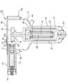
図1において、本実施例のマイクロフォーカスX線管(以下、X線管と略称する)10は、電子線を発生する陰極12と、電子線が衝突してX線を発生する陽極14と、陰極12と陽極14を真空気密に内包し、絶縁支持する外囲器16とから構成される。本実施例のX線管10では、マイクロフォーカス(微小焦点)が得られ、かつ大きなX線管電流で動作させることができる陰極12の構成に特徴がある。陰極12の構成、動作については、後で図2〜図9を用いて詳しく説明する。それに先立って、陰極12を除いた全体構造について図1により説明する。
In FIG. 1, a microfocus X-ray tube (hereinafter abbreviated as an X-ray tube) 10 of the present embodiment includes a
図1において、陽極14はX線管としての許容負荷を大きくするために回転陽極形の構造を採用している。この陽極(以下、回転陽極とも呼ぶ)14はこれに限定されず、固定陽極形のものでもよい。回転陽極14はX線発生源となる円盤状のターゲット18と、ターゲット18を支持するロータ20と、ロータ20を支持する回転軸22と、回転軸22を回転自在に支持する軸受24と、軸受24を支持する固定部26などから構成される。この回転陽極14は全体として汎用の医療用回転陽極X線管のものとほぼ同じ構造をしている。ターゲット18は傘型で円盤状をしており、タングステンまたはその合金などの高原子番号で、高融点の金属材料から成る。ターゲット18の傾斜面には、陰極12からの細いビーム状の電子線50が衝突し、焦点28が形成される。
In FIG. 1, the
次に、外囲器16は、回転陽極14のターゲット18と陰極12の先端部を囲み、アース(接地)電位に保持される大径部30と、回転陽極14の固定部26と結合されて、これを絶縁支持する陽極絶縁部32と、陰極12を絶縁支持する陰極絶縁部34とから構成される。大径部30は大略円板状の円板部36と、大略円筒状をした大径肉厚の円筒部38とが結合されたもので、円板部36と円筒部38は銅やステンレス鋼などの金属材料から成る。円板部36の回転陽極14のターゲット18上の焦点28に近接する部分に設けた開口36aにX線放射窓40が取り付けられる。円板部36の開口36aの形状はX線放射窓40の形状に合わせて加工され、円形や長方形などがあるが、通常は円形である。X線放射窓40はX線透過性の良いベリリウムなどから成り、窓枠などを介して、円板部36の開口36aに溶接またはろう付けによって結合されている。陽極絶縁部32は回転陽極14のロータ20の外径より少し太い円筒部42と、大径部30の円筒部38に結合するためにコーン状に広げられたフレア部44と、回転陽極14の固定部26と結合するための陽極接続部46とから構成される。陽極絶縁部32は大部分が耐熱性ガラスやセラミックなどの絶縁物から成り、両端の大径部30の円筒部38や回転陽極14の固定部26との接続部分には絶縁物となじみの良い金属材料が使用されている。大径部30の円筒部38の側面には、回転陽極14の中心軸48とほぼ直交する方向に、陰極絶縁部34が結合されている。陰極絶縁部34は細い外径の円筒形状をしており、その一端において、大径部30の円筒部38の側面に結合され、その他端において陰極12のステム70と結合されている。陰極絶縁部34の大部分は耐熱性ガラスまたはセラミックなどの絶縁物から成る。
Next, the
図1において、外囲器16の大径部30の円筒部38の中心軸と回転陽極14の中心軸48はほぼ一致し、回転陽極14のターゲット18は大径部30のほぼ中心に位置することになる。陰極12の中心軸が回転陽極14のターゲット18上の焦点28にほぼ一致するように、陽極絶縁部32は大径部30の円筒部38の側面に結合される。その結果、陰極12からの電子線50はターゲット18上の焦点28に衝突し、焦点28で発生したX線52は大径部30の円板部36に取り付けられたX線放射窓40を通して外部に(図示の上方に)取り出される。
In FIG. 1, the central axis of the
次に、図2〜図9を用いて、本実施例のX線管10の要部である陰極12の構成と動作について説明する。先ず、図2により、X線管10の陰極12の構造について説明する。図2において、図2(a)は陰極の全体構造図、図2(b)は陰極の電子集束系の拡大図である。図2において、陰極12は電子線50を発生するカソード54と、電子線50を集束する電子集束系56と、カソード54を支持するカソード支持体58と、電子集束系56を構成する3個のグリッド電極60、62、64を絶縁支持する電子集束系絶縁体66と、電子集束系絶縁体66を覆う陰極カバー68と、カソード54や電子集束系56などを支持するステム70などで構成される。
Next, the configuration and operation of the
カソード54は、酸化物または含浸形のカソードで、加熱用のヒータを備えている。カソード54は、ヒータの加熱によって1000K以上の高温で動作し、熱電子を放射する。カソード54は底付きの円筒形状をしており、円筒の内側にヒータが絶縁して配設され、円筒の底の外表面(以下、電子放射面という)54aから熱電子が放射される。カソード54はカソード支持体58に支持され、更に電子集束系56を介して電子集束系絶縁体66に支持される。電子集束系56は本実施例では3個のグリッド電極60、62、64で構成される。すなわち、カソード54に最も近い第1グリッド電極(以下、G1電極と略称する)60と、次に近い第2グリッド電極(以下、G2電極と略称する)62と、3番目に近い第3グリッド電極(以下、G3電極と略称する)64である。電子集束系56を構成するグリッド電極の個数は3個に限定されず、4個以上であってもよい。3個のグリッド電極60、62、64はそれぞれ中心部に電子線50を通す開口60a、62a、64aを有し、カソード54と回転陽極14のターゲット18との間に、カソード54の側からG1電極60、G2電極62、G3電極64の順で、適当な間隔をとって同軸に配置される。
The
電子集束系56の中で、G1電極60とG2電極62は板状体で、その中心部に小さい直径の開口60a、62aが設けられており、全体としては取り付けなどを考慮してカップ状に形成されている。G3電極64は中心部に大きな開口64aが設けられており、全体としては円筒形に近い形状をしている。本実施例では、G1電極60の開口60aの内周面は電子集束系56の中心軸72に対しテーパーの付いた面74に加工されており、その内径はカソード54側で最も小さくなっている。このテーパー面74は後で説明する如く、G1電極60とG2電極62との間に形成されるカソードレンズの集束効率を改善するものである。テーパー面74のテーパー角度は図示の例では約27°となっているが、このテーパー角度は電子集束系の構成に応じて適宜変えられる。G2電極62の開口62aの内周面は従来品と同様電子集束系56の中心軸72と平行な円筒面である。また、G3電極64の開口64aの内周面も電子集束系56の中心軸72に対しテーパーの付いた面76に加工されており、その内径はカソード54側で最も大きくなっている。このテーパー面76は、図示のものでは約15°となっているが、このテーパー角度も電子集束系の構成に応じて適宜変えられる。また、G2電極62の開口62aの内径はG1電極60の開口60aの最小内径の1/2以上としている。これは、電子線50の中心軸72から離れた位置を走行する電子がG2電極62の開口62aの近傍に衝突するのを防止するためであり、通常G2電極62の開口62aの内径はG1電極60の開口60aの最小内径とほぼ同程度の寸法に設定されている。G1電極60、G2電極62、G3電極64の開口60a、62a、64aの形状と寸法及びそれぞれの間の間隔は、所望の焦点寸法やそれぞれのグリッド電極60、62、64に印加する電圧と関係して決定される。このグリッド電極に印加する電圧(以下、グリッド電圧という)はカソード54に印加する電位(以下、カソード電位または陰極電位という)を基準にして指定される。また、グリッド電極60、62、64の材料としては耐熱性金属材料が用いられるが、本発明ではグリッド電極60、62、64に入射する高エネルギーの電子線は従来品に比べて少なくなるので、ステンレス鋼などが使用可能となり、従来品の如くモリブデンなどの高融点金属材料を使用せずに済む。これにより材料費や加工費などの低減が期待できる。
In the
電子集束系56の3個のグリッド電極60、62、64の支持は、各グリッド電極間の絶縁を保つために2個の棒状の絶縁物66aから成る電子集束系絶縁体66によって行われる。この棒状の絶縁物66aは耐熱性ガラスなどから成るが、この絶縁物66aとグリッド電極60、62、64との結合は、それぞれのグリッド電極の外周に溶接などで取り付けた取付金具66bに絶縁物66aを溶着することによって行われる。絶縁物66aとしては耐熱性ガラス以外にセラミックが用いられる場合もあるが、その場合には絶縁物66aと取付金具66bはろう付けなどで結合される。電子集束系絶縁体66はリング状の支持体78を介してステム70に支持される。ステム70は円板状の絶縁物から成る支持板70aと、この支持板70aを貫通する複数本のリード線80と、支持板70aの外周に結合されたリング状の接続筒70bと、支持体78を支持する円筒状の電子集束系支持部70cなどから構成される。支持板70aはセラミックなどの耐熱性絶縁物から成り、支持板70aとリード線80、接続筒70b、電子集束系支持部70cとはろう付けにより結合されている。リード線80はヒータ加熱電圧、カソード電位、グリッド電圧などを供給するためのものである。接続筒70bは支持板70aの材料となじみの良い金属材料から成り、外囲器16の陰極絶縁部34の端部に設けられた円筒状の接続金具34aに溶接などによって結合される。この結合によって陰極12全体が外囲器16に支持される。また、この結合時に、回転陽極14のターゲット18と陰極12の先端部との間隔が調整される。電子集束系支持部70cは薄肉の円筒で、リード線80を囲むように配置され、その一端は支持板70aに結合され、その他端は電子集束系絶縁体66を支持する支持体78に結合されている。この電子集束系支持部70cの側面には複数個の開口が設けられており、この開口を用いて、リード線80と陰極12の各電極との電気的接続が行われる。
The three
電子集束系56と回転陽極14のターゲット18との間には、ターゲット18からの反射電子が陰極12の電子集束系56やその他の部分に到達しないようにするため、ステンレス鋼などの耐熱性金属材料から成る陰極カバー68が配置される。この陰極カバー68は底付きの円筒形状をしており、その円筒部68が外囲器16の大径部30に直接接続されている。陰極カバー68と大径部30との接続は、直接結合してもよいが、間に金属材料などからなる媒体を介して接続してもよい。陰極カバー68のターゲット18に対向する面(底面)68bには電子線50が通過するための開口84が設けられており、陰極カバー68は電子集束系56や電子集束系絶縁体66を覆うように配置されている。陰極カバー68の開口84の直径は電子集束系56のG3電極64の開口64aの直径よりも大きいが、グリッド電極60、62、64を絶縁支持する電子集束系絶縁体66の2本の絶縁物66aの間隔より小さくしている。すなわち、陰極カバー68の開口84の大きさはターゲット18上の焦点28から絶縁物66aが直視できないように隠す大きさとしている。これにより、ターゲット18の焦点28からの反射電子が絶縁物66aに到達するのを防止している。陰極カバー68は、その開口84が電子集束系56の中心軸72と同軸で、G3電極64の開口64aに近接するように配置されている。また、陰極カバー68は外囲器16の大径部30と接続されることで、大径部30と同電位となり、アース電位に保持される。このように、陰極12の電子集束系56及びその周辺部をアース電位の陰極カバー68にて覆い、かつターゲット18に対向する底面68bの電子線50の通過する開口84を必要最小限の面積の穴とすることにより、ターゲット18の焦点28からの反射電子は陰極カバー68や大径部30に向かい、その後アースに流れて行くことになるので、電子集束系絶縁体66の絶縁物66aに帯電することを防止することができる。
In order to prevent the reflected electrons from the
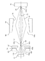
次に、図3〜図9を用いて、本実施例のX線管の電子集束系における電子線の集束状況を従来品の電子集束系と比較しながら説明する。図3と図4には本実施例と従来品の電子集束系の概略構成と電子線の概略形状を示す。また、図5と図6には本実施例と従来品の電子集束系のG1電極及びG2電極附近での電子軌道の計算例を示す。図3と図4において、本実施例の電子集束系56と従来品の電子集束系86とを比較すると、G1電極とG3電極の開口の内周面の形状とG2電極の開口の直径が異なる。すなわち、従来品のG1電極88とG3電極92の開口88a、92aの内周面が電子集束系の中心軸72に対し平行であるのに対し、本実施例のG1電極60とG3電極64の開口60a、64aの内周面はテーパー面74、76であり、G1電極60のテーパー面74はテーパー角度が約27°で、ターゲット18側に行くにつれて内周面の直径が大きくなるものであり、G3電極64のテーパー面76はテーパー角度が約15°で、ターゲット18側に行くにつれて内周面の直径が小さくなるものである。また、本実施例のG2電極62の開口62aの直径は従来品のG2電極90の開口90aの直径よりも格段に大きく、G1電極60の開口60aの最小直径とほぼ同程度になっている。電子集束系の各グリッド電極に印加されるグリッド電圧は、両方のX線管でほぼ同じ電圧が印加され、G1電極60、88には数十Vの正電位が、G2電極62、90には数百〜数千Vの正電位が、G3電極64、92には数千Vの正電位が、それぞれ印加される。これらのグリッド電圧はいずれもカソード電位を基準にしたものである。また、X線管の陰極(カソード)と陽極(ターゲット)との間にはX線管電圧が印加される。この結果、電子線50の集束において、G2電極の近傍に形成されるクロスオーバー(カソード側クロスオーバー)については、本実施例のクロスオーバー94は従来品のクロスオーバー96よりG2電極から離れた位置に形成され、またターゲット18上の焦点28の寸法については本実施例のもののほうが従来品のものより若干小さ目になっている。また、図5と図6を比較して判るように、従来品のG2電極90の開口90aの近傍に一部の電子線50が衝突しているのに対し、本実施例のG2電極62では開口62a近傍への電子線50の衝突の恐れは全くなくなっている。
Next, the electron beam focusing state in the electron focusing system of the X-ray tube of the present embodiment will be described using FIGS. 3 to 9 in comparison with the conventional electron focusing system. 3 and 4 show the schematic configuration of the electron focusing system of this embodiment and the conventional product and the schematic shape of the electron beam. 5 and 6 show calculation examples of the electron trajectory in the vicinity of the G1 electrode and the G2 electrode in the electron focusing system of this embodiment and the conventional product. 3 and 4, when comparing the
次に、図7と図8を用いて、従来品と本実施例の電子集束系における電子線の集束状況について説明する。両図において簡単のため、電子線50としては、電子集束系の中心軸72の近くを走行する内側の電子線と、中心軸72から離れて走行する外側の電子線を代表として選び、電子線の走行も直線で近似して、それぞれの電子線の集束状況を説明することにした。図7において、従来品の電子集束系86のG1電極88、G2電極90、G3電極92の開口88a、90a、92aの内周面は上記の如く中心軸72と平行で、G2電極90の開口90aの直径は小さくなっている。このような構成の電子集束系86では、内側の電子線98はG2電極90の開口90aからG3電極92側に少し寄った位置にカソード側クロスオーバー(以下、内側ビームカソード側クロスオーバーという)100を形成し、更にターゲット18上にターゲット側クロスオーバー(以下、内側ビームターゲット側クロスオーバーという)101を形成する。これに対し、外側の電子線102はG2電極90の開口90aの中にカソード側クロスオーバー(以下、外側ビームカソード側クロスオーバーという)104を形成し、更にターゲット18の少し手前にターゲット側クロスオーバー(以下、外側ビームターゲット側クロスオーバーという)105を形成する。その結果、従来品の電子集束系86ではターゲット18上には少し大きめの微小焦点が形成される。また、従来品の電子集束系86ではG2電極90の開口90aの直径が小さいため、図6に示す如く、外側の電子線102のうちの一部である、より外側のものはG2電極90の開口90aの近傍に衝突し、G2電極90を温度上昇させる原因となっていた。
Next, the focusing state of the electron beam in the electron focusing system of the conventional product and the present embodiment will be described with reference to FIGS. For the sake of simplicity in both figures, the
図8において、本実施例の電子集束系56では、G1電極60とG3電極64の開口60a、64aの内周面にテーパー面74、76を設け、G2電極62の開口62aの直径をG1電極60の開口60aの最小直径とほぼ同じぐらいにしている。このような構成の電子集束系56では、図5に示す如く、G1電極60とG2電極62との間の電位分布が改善され、両電極によってこの部分に形成されるカソードレンズによる電子線50の集束がゆるやかとなり、特に外側の電子線110に対する集束がゆるやかとなっている。また、G3電極64によって形成される主レンズによる電子線50の集束はきつくなっており、特に外側の電子線110に対する集束がきつくなっている。カソード54の電子放射面54aから放射された内側の電子線106はG1電極60とG2電極62で形成されるカソードレンズにより集束されて、従来品の電子集束系86の場合とほぼ同様に、G2電極62の開口からG3電極64に少し寄った位置に内側ビームカソード側クロスオーバー108を形成し、更にG3電極64によって形成される主レンズにより集束されてターゲット18上に内側ビームターゲット側クロスオーバー109を形成する。また、外側の電子線110は改善されたカソードレンズによってゆるやかに集束されて、従来品の電子集束系86の場合よりもカソード54から離れた、内側ビームカソード側クロスオーバー108とほぼ同じ位置に外側ビームカソード側クロスオーバー112を形成する。その結果、内側ビームカソード側クロスオーバー108の位置と外側ビームカソード側クロスオーバー112の位置がほぼ一致するために、小径のカソード側クロスオーバー94が得られる。更に、外側の電子線110は従来品よりカソード54から離れた位置にある外側ビームカソード側クロスオーバー112から出発するが、G3電極64に形成される改善された主レンズによってきつく集束されて、ターゲット18上に外側ビームターゲット側クロスオーバー113を形成する。その結果、ターゲット18上には内側ビームターゲット側クロスオーバー109と外側ビームターゲット側クロスオーバー113とが一緒になった、小径のクロスオーバー94に対応する小さい焦点が得られる。
In FIG. 8, in the
また、本実施例では、電子集束系56のG3電極64の開口64の内周面を、その直径がターゲット18側に行くにつれて小さくなるテーパー面76としたが、このテーパー面76はこれに限定されず、逆傾斜の場合もあり得る。すなわち、外側の電子線110をきつく集束する場合には、テーパー面76は図8に示したような傾斜で形成され、反対に外側の電子線110をゆるく集束する場合には、テーパー面76はその直径がターゲット18側に行くにつれて大きくなるように形成される。また、テーパー面76のテーパー角度は外側の電子線110を主レンズで集束する場合のきつさ及びゆるさの度合いに応じて変えられる。
Further, in this embodiment, the inner peripheral surface of the
また、図8において、本実施例の電子集束系56では、G2電極62の開口62aの直径を従来品のG2電極に比べ格段に大きくしているので、図5に示す如く、外側の電子線110もG2電極62に衝突することなく集束される。その結果、G2電極62が電子線50によって加熱されて、高温になることはなくなるので、グリッド電極間で放電したりする問題もなくなった。
In FIG. 8, in the
図9は、本実施例と従来品とのターゲット上に形成される焦点の電流密度分布を比較して示したものである。図9において、横軸はターゲット上の位置座標、縦軸は電子線の電流密度である。図において、カーブAは本実施例のもの、カーブBは従来品のものである。本実施例の場合、同じX線管電流では電子線の電流密度は従来品に比べ、大幅に増加し、焦点寸法も小さくなっている。ターゲット上の焦点寸法としては、本実施例のものは従来品に比べ、約20%程度小さいものが得られている。本実施例の電子集束系では、X線管電流を増加しても、電子線の集束状況は殆んど変化することがないので、微小焦点を維持することができる。 FIG. 9 shows a comparison of the current density distributions of the focal points formed on the target of this example and the conventional product. In FIG. 9, the horizontal axis represents the position coordinates on the target, and the vertical axis represents the current density of the electron beam. In the figure, curve A is that of this embodiment, and curve B is that of a conventional product. In the case of the present embodiment, the current density of the electron beam is greatly increased and the focal spot size is reduced as compared with the conventional product with the same X-ray tube current. As the focal spot size on the target, the present embodiment has a size about 20% smaller than that of the conventional product. In the electron focusing system of this embodiment, even if the X-ray tube current is increased, the focusing state of the electron beam hardly changes, so that the micro focus can be maintained.
図10には、本発明に係るマイクロフォーカスX管のG1電極及びG3電極の開口の内周面の形状の他の例を示す。本実施例のX線管10では電子集束系56のG1電極60及びG3電極64の開口60a、64aの内周面の形状としてテーパー面74、76を示したが、開口60a、64aの内周面の形状はこれに限定されず、図10に示すような他の形状であってもよい。図10の各図はG1電極またはG3電極(以下、グリッド電極で代表する)の中心軸72の上側断面を示したものである。図10(a)の第1の他の例では、グリッド電極114の開口114aの内周面は第1のテーパー面116と第2のテーパー面118を接続して形成されており、テーパー面の傾斜角度は第1のテーパー面116の方が大きい。図10(b)の第2の他の例では、グリッド電極114の開口114aの内周面は第1のテーパー面116と円筒面120と第2のテーパー面118を接続して形成されている。図10(c)の第3の他の例では、グリッド電極114の開口114aの内周面は3個のテーパー面、すなわち第1のテーパー面116と第2のテーパー面118と第3のテーパー面121を接続して形成されている。上記のテーパー面はいずれも開口114aの内周面の直径が右側に行くにつれて、すなわちカソード54から離れるにつれて小さくなっている。図10(d)の第4の他の例では、グリッド電極114の開口114aの内周面は曲面122で形成されている。図10(e)の第5の他の例では、グリッド電極114の開口114aの内周面は曲面122とテーパー面116を接続して形成されている。上記の曲面122も開口114aの内周面の直径は右側に行くにつれて小さくなっている。図10(f)〜図10(g)の第6〜第10の他の例は図10(a)〜図10(e)の第1〜第5の他の例の構造図の左右を反転させたもので、それぞれのグリッド電極の開口の内周面の直径は右側(ターゲット側)に行くにつれて増加するか、または少なくとも減少しないように形成されている。逆に、図10(a)〜図10(e)の第1〜第5の他の例のそれぞれのグリッド電極の開口の内周面の直径は右側(ターゲット側)に行くにつれて減少するか、または少なくとも増加しないように形成されている。
FIG. 10 shows another example of the shape of the inner peripheral surface of the openings of the G1 electrode and the G3 electrode of the microfocus X tube according to the present invention. In the
G1電極としては、この開口の内周面の形状によって、外側の電子線をゆるく集束するような電位分布をG1電極の近傍に作る必要性から、第1の実施例のG1電極や図10(f)、図10(i)などの、開口の内周面の直径がターゲット側(図示の右側)に行くにつれて増加するか、または少なくとも減少しないように形成されているもので、構造の簡単なものが適している。これに対し、G3電極としては、第1の実施例の如く、外側の電子線をきつく集束するような電位分布をG3電極の近傍に作る必要がある場合と、その他に外側の電子線をゆるく集束するような電位分布をG3電極の近傍に作る必要がある場合とがあるため、図2の本実施例のG3電極64や図10(a)〜図10(e)などの開口の直径がターゲット側に行くにつれて減少するか、または少なくとも増加しないように形成されているものと、図2の本実施例のG3電極64を左右反転させたものや図10(f)〜図10(g)などの、開口の直径がターゲット側に行くにつれて増加するか、または少なくとも減少しないように形成されているものの両方が適している。
As the G1 electrode, the shape of the inner peripheral surface of this opening makes it necessary to create a potential distribution in the vicinity of the G1 electrode so as to focus the outer electron beam loosely. Therefore, the G1 electrode of the first embodiment and FIG. f) The diameter of the inner peripheral surface of the opening, such as FIG. 10 (i), is formed so that it does not increase or at least does not decrease as it goes to the target side (the right side in the figure). Things are suitable. On the other hand, as for the G3 electrode, as in the first embodiment, it is necessary to create a potential distribution in the vicinity of the G3 electrode so as to focus the outer electron beam tightly. Since there is a case where it is necessary to create a potential distribution that converges in the vicinity of the G3 electrode, the diameter of the
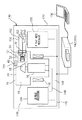
次に、図11を用いて、本発明に係るX線発生装置の一実施例について説明する。図11は、本実施例のX線発生装置の構成図である。図11において、本実施例のX線発生装置130は、本発明に係るマイクロフォーカスX線管10と、X線管10を内包する容器132と、X線管10の回転陽極14及び陰極12に高電圧を供給する高電圧発生回路134と、X線管10の陰極12の電子集束系を構成するグリッド電極にグリッド電圧を供給するグリッド電圧発生回路136と、X線管10の回転陽極14を回転駆動するステータ138と、X線管10や高電圧発生回路134やグリッド電圧発生回路136などを絶縁するための絶縁油140と、制御回路142などから構成される。
Next, an embodiment of the X-ray generator according to the present invention will be described with reference to FIG. FIG. 11 is a configuration diagram of the X-ray generator of the present embodiment. In FIG. 11, the
容器132は通常金属板などから成る筐体で、形状は直方体のものが多い。容器132内にはX線管10以外に高電圧発生回路134やグリッド電圧発生回路136などが含まれ、絶縁油140が充填されている。容器132の内壁の一部で、X線管10の回転陽極14のターゲット18に近い部分には防X線のために鉛板などが張られている。X線管10の回転陽極14と高電圧発生回路134とグリッド電圧発生回路136は絶縁物などから成る支持体を介して容器132の内壁に支持されている。X線管10の外囲器16の大径部30は容器132の内壁に直接支持され、その内壁のX線管10のX線放射窓40に対向する部分に、X線を外部に取り出すための開口(X線放射口)144が設けられている。ステータ138はX線管10の回転陽極14のロータの周囲に配置され、容器132の内壁などに絶縁物を介して支持される。
The
高電圧発生回路134は高電圧変圧器と整流回路などで構成され、制御回路142から商用周波数の交流電圧が低電圧リード線146を経由して供給されて、これを高電圧変圧器にて交流の高電圧に昇圧した後、整流回路で整流する。高電圧発生回路134としては通常中性点接地方式が用いられ、正の高電圧と負の高電圧を発生する。正の高電圧は高電圧リード線148を経由してX線管10の回転陽極14へ、負の高電圧は高電圧リード線148及びグリッド電圧発生回路136を経由してX線管10の陰極12へ供給される。グリッド電圧発生回路136は電圧調整器と絶縁変圧器と整流回路などから構成される。本実施例ではグリッド電圧がグリッド電極毎に異なるので、3個のグリッド電圧を発生するために、電圧調整器などは3組用いられている。グリッド電圧発生回路136では制御回路142から供給される商用周波数の交流電圧を電圧調整器で適当な電圧値に調整して、絶縁変圧器にて絶縁した高電位の交流電圧とした後、整流回路で整流してグリッド電圧とする。グリッド電圧はグリッド電圧発生回路136からグリッドリード線150及びX線管10のステム70のリード線を経由して、電子集束系56のG1電極、G2電極及びG3電極に供給される。また、グリッド電圧発生回路136には陰極12のカソード54を加熱するためのヒータの電源回路も含まれている。ヒータ電源回路は電圧調整器と絶縁変圧器などから構成され、制御回路142から供給された商用周波数の交流電圧を電圧調整器で適当な電圧値に調整した後、絶縁変圧器にて絶縁した高電位のヒータ加熱電圧とする。ヒータ加熱電圧はグリッド電圧発生回路136からヒータリード線152及びステム70のリード線を経由してカソード54のヒータに供給される。
The high
制御回路142は、X線管10を動作させるための電源部154と、X線管10の動作を制御する制御部156などから構成される。電源部154には、高電圧発生回路134の1次電源やグリッド電圧発生回路(ヒータ加熱回路を含む)136の1次電源やステータ駆動電源などが含まれる。制御部156には、X線管10の負荷などを制御するためのコンピュータ(CPU)などが含まれる。この制御回路142は上記の如くX線発生装置130に組み込まれる場合もあるが、多くの場合はX線装置の制御装置の中に含まれ、この制御装置によってX線発生装置の制御が行われる。
The
次に、図12を用いて、本発明に係るX線装置の一実施例について説明する。図12は本発明に係るX線装置の一実施例の概略構成図である。図12において、本実施例のX線装置160は、X線を発生するX線発生装置130と、被検体162を透過したX線量を検出するX線検出装置164と、X線検出装置164からの出力信号に基づいて被検体162のX線画像を形成する画像形成装置166と、X線発生装置130、X線検出装置164、画像形成装置166の動作を制御する制御装置168などから構成される。ここで、X線発生装置130は図11に示したような本発明に係るX線発生装置で、その中には本発明に係るマイクロフォーカスX線管10が含まれている。
Next, an embodiment of the X-ray apparatus according to the present invention will be described with reference to FIG. FIG. 12 is a schematic configuration diagram of an embodiment of an X-ray apparatus according to the present invention. In FIG. 12, an
X線検出装置164としては、ラインセンサーのようにX線検出素子を線状に配列したものや、イメージインテンシファイア(I.I.)などのようにX線検出素子を面状に配列したものなどが用いられる。X線検出装置164では、通常X線素子から受光したX線量に対応した強度の電気信号が出力されるので、画像形成装置166ではX線検出装置164からの線状または面状に分布した電気信号に基づいて、面状画像であるX線画像を形成する。また、X線検出手段としてX線フィルムを用いる場合には、X線フィルムがX線検出装置164に対応し、フィルム現像装置などが画像形成装置166に対応することになる。制御装置168では、マイクロフォーカスX線管10を駆動するための条件の制御、X線検出装置164のX線検出動作の制御や画像形成装置166の画像作成動作の制御などを行う。また、制御装置168は、X線発生装置130をはじめとする他の装置への電源電圧の供給なども行う。
The
本発明に係るX線発生装置やX線装置では、本発明に係るマイクロフォーカスX線管を内包しているので、微小焦点と大きなX線管電流が得られ、微小焦点によるX線拡大撮影による診断や微細な内部構造の非破壊検査において高精細なX線画像が得られるとともに、安定した動作を長く維持することができる。 Since the X-ray generator and X-ray apparatus according to the present invention include the microfocus X-ray tube according to the present invention, a microfocus and a large X-ray tube current can be obtained, and X-ray magnified imaging with a microfocus is performed. High-definition X-ray images can be obtained in diagnosis and non-destructive inspection of fine internal structures, and stable operation can be maintained for a long time.
10・・・マイクロフォーカスX線管(X線管)
12・・・陰極
14・・・陽極(回転陽極)
16・・・外囲器
18・・・ターゲット
26・・・固定部
28・・・焦点
30・・・大径部
32・・・陽極絶縁部
34・・・陰極絶縁部
36・・・円板部
38・・・円筒部
40・・・X線放射窓
48、72・・・中心軸
50・・・電子線
52・・・X線
54・・・カソード
54a・・・電子放射面
56、86・・・電子集束系
58・・・カソード支持体
60、88・・・第1グリッド電極(G1電極)
60a、62a、64a、84、114a・・・開口
62、90・・・第2グリッド電極(G2電極)
64、92・・・第3グリッド電極(G3電極)
66・・・電子集束系絶縁体
66a・・・絶縁物
68・・・陰極カバー
68a・・・円筒部
68b・・・底面
70・・・ステム
74、76・・・テーパー面
94、96・・・クロスオーバー(カソード側クロスオーバー)
98、106・・・内側の電子線
100、108・・・内側ビームカソード側クロスオーバー
101、109・・・内側ビームターゲット側クロスオーバー
102、110・・・外側の電子線
104、112・・・外側ビームカソード側クロスオーバー
105、113・・・外側ビームターゲット側クロスオーバー
114・・・グリッド電極
116、123・・・第1のテーパー面(テーパー面)
118、124・・・第2のテーパー面
120・・・円筒面
121、125・・・第3のテーパー面(テーパー面)
122、126・・・曲面
130・・・X線発生装置
132・・・容器
134・・・高電圧発生回路
136・・・グリッド電圧発生回路
140・・・絶縁油
142・・・制御回路
160・・・X線装置
162・・・被検体
164・・・X線検出装置
166・・・画像形成装置
168・・・制御装置
10 ... Microfocus X-ray tube (X-ray tube)
12 ... Cathode
14 ... Anode (rotary anode)
16 ... Envelope
18 ... Target
26 ・ ・ ・ Fixing part
28: Focus
30 ... Large diameter part
32 ... Anode insulation
34 ・ ・ ・ Cathode insulation
36 ... disk part
38 ... Cylindrical part
40 ... X-ray radiation window
48, 72 ... Center axis
50 ... electron beam
52 ... X-ray
54 ・ ・ ・ Cathode
54a ・ ・ ・ Electron emitting surface
56, 86 ... Electronic focusing system
58 ... Cathode support
60, 88 ... 1st grid electrode (G1 electrode)
60a, 62a, 64a, 84, 114a ... opening
62, 90 ... Second grid electrode (G2 electrode)
64, 92 ... Third grid electrode (G3 electrode)
66 ・ ・ ・ Electronic focusing insulator
66a ・ ・ ・ Insulator
68 ・ ・ ・ Cathode cover
68a ・ ・ ・ Cylindrical part
68b ・ ・ ・ Bottom
70 ... Stem
74, 76 ... Tapered surface
94, 96 ... crossover (cathode side crossover)
98, 106 ... Inner electron beam
100, 108 ... Inner beam cathode side crossover
101, 109 ... Inner beam target side crossover
102, 110 ... Outside electron beam
104, 112 ... Outer beam cathode side crossover
105, 113 ... Crossover on the outer beam target side
114 ・ ・ ・ Grid electrode
116, 123 ... 1st taper surface (taper surface)
118, 124 ... second tapered surface
120 ... Cylindrical surface
121, 125 ... Third taper surface (taper surface)
122, 126 ... curved surface
130 ... X-ray generator
132 ・ ・ ・ Container
134 ・ ・ ・ High voltage generator
136 ... Grid voltage generator
140 ・ ・ ・ Insulating oil
142 ... Control circuit
160 ... X-ray equipment
162 ... Subject
164 ... X-ray detector
166 ... Image forming apparatus
168 ... Control device
Claims (4)
前記電子集束系は少なくとも3個のグリッド電極から成り、
前記グリッド電極のうちの前記カソードに最も近接するグリッド電極(G1電極)の開口の内周面は、その直径がカソード側で最も小さく、ターゲット側で最も大きく、前記カソードに3番目に近接するグリッド電極(G3電極)の開口の内周面は、その直径がカソード側で最も大きく、ターゲット側で最も小さいことを特徴とするマイクロフォーカスX線管。 The electron beam collides with a cathode having an electron beam generating cathode and an electron focusing system composed of a plurality of grid electrodes arranged in the electron beam path for focusing the electron beam into a thin linear beam. An anode having a target for generating X-rays, and an envelope that insulates and supports the cathode and the anode, and is sealed in a vacuum-tight manner, and each of the plurality of grid electrodes of the cathode electron focusing system passes through the electron beam. An electron lens for focusing an electron beam by applying a potential with respect to the cathode to each grid electrode, and having a grid electrode insulating support portion for insulating and supporting the grid electrode In microfocus X-ray tube,
The electron focusing system comprises at least three grid electrodes;
The inner peripheral surface of the opening of the grid electrode (G1 electrode) which is closest to said cathode of said grid electrode has a diameter smallest at the cathode side, rather most size at the target side, close to the third to the cathode A microfocus X-ray tube characterized in that the inner peripheral surface of the opening of the grid electrode (G3 electrode) has the largest diameter on the cathode side and the smallest on the target side .
Priority Applications (1)
| Application Number | Priority Date | Filing Date | Title |
|---|---|---|---|
| JP2005101664A JP4619176B2 (en) | 2005-03-31 | 2005-03-31 | Microfocus X-ray tube |
Applications Claiming Priority (1)
| Application Number | Priority Date | Filing Date | Title |
|---|---|---|---|
| JP2005101664A JP4619176B2 (en) | 2005-03-31 | 2005-03-31 | Microfocus X-ray tube |
Publications (3)
| Publication Number | Publication Date |
|---|---|
| JP2006286264A JP2006286264A (en) | 2006-10-19 |
| JP2006286264A5 JP2006286264A5 (en) | 2008-02-07 |
| JP4619176B2 true JP4619176B2 (en) | 2011-01-26 |
Family
ID=37407977
Family Applications (1)
| Application Number | Title | Priority Date | Filing Date |
|---|---|---|---|
| JP2005101664A Expired - Fee Related JP4619176B2 (en) | 2005-03-31 | 2005-03-31 | Microfocus X-ray tube |
Country Status (1)
| Country | Link |
|---|---|
| JP (1) | JP4619176B2 (en) |
Families Citing this family (8)
| Publication number | Priority date | Publication date | Assignee | Title |
|---|---|---|---|---|
| JP4963622B2 (en) * | 2007-04-03 | 2012-06-27 | 浜松ホトニクス株式会社 | X-ray tube |
| JP6168770B2 (en) * | 2012-12-28 | 2017-07-26 | キヤノン株式会社 | Radiation generation unit and radiography system |
| JP6498535B2 (en) * | 2015-06-10 | 2019-04-10 | キヤノン電子管デバイス株式会社 | X-ray tube |
| DE102017105546B4 (en) * | 2017-03-15 | 2018-10-18 | Yxlon International Gmbh | Socket for receiving a plug of a high-voltage cable for a microfocus X-ray tube, plug connection for a high-voltage cable |
| CN108962707B (en) * | 2018-08-16 | 2023-11-28 | 成都凯赛尔电子有限公司 | Micro-focus cold cathode focusing structure and mounting method thereof |
| US10910190B2 (en) * | 2019-01-10 | 2021-02-02 | Electronics And Telecommunications Research Institute | X-ray tube |
| CN115841935B (en) * | 2023-02-20 | 2023-05-12 | 安徽科昂新材料科技有限公司 | X-ray source device |
| CN117637417A (en) * | 2024-01-24 | 2024-03-01 | 电子科技大学 | Micro-focus electron gun using aperture structure for auxiliary focusing |
Citations (2)
| Publication number | Priority date | Publication date | Assignee | Title |
|---|---|---|---|---|
| JP2002008572A (en) * | 2000-06-20 | 2002-01-11 | Shimadzu Corp | X-ray tube |
| JP2005038825A (en) * | 2003-06-26 | 2005-02-10 | Hitachi Medical Corp | Microfocus x-ray tube and x-ray apparatus using the same |
Family Cites Families (1)
| Publication number | Priority date | Publication date | Assignee | Title |
|---|---|---|---|---|
| IL71676A0 (en) * | 1984-04-27 | 1984-12-31 | Israel State | X-ray tube |
-
2005
- 2005-03-31 JP JP2005101664A patent/JP4619176B2/en not_active Expired - Fee Related
Patent Citations (2)
| Publication number | Priority date | Publication date | Assignee | Title |
|---|---|---|---|---|
| JP2002008572A (en) * | 2000-06-20 | 2002-01-11 | Shimadzu Corp | X-ray tube |
| JP2005038825A (en) * | 2003-06-26 | 2005-02-10 | Hitachi Medical Corp | Microfocus x-ray tube and x-ray apparatus using the same |
Also Published As
| Publication number | Publication date |
|---|---|
| JP2006286264A (en) | 2006-10-19 |
Similar Documents
| Publication | Publication Date | Title |
|---|---|---|
| JP4619176B2 (en) | Microfocus X-ray tube | |
| KR20140049471A (en) | X-ray generating apparatus | |
| US9653248B2 (en) | X-ray tube | |
| US7067820B2 (en) | Particle-optical apparatus with a permanent-magnetic lens and an electrostatic lens | |
| US9431206B2 (en) | X-ray generation tube, X-ray generation device including the X-ray generation tube, and X-ray imaging system | |
| US20070051907A1 (en) | Device for generating X-ray or XUV radiation | |
| JP6619916B1 (en) | X-ray generator tube, X-ray generator and X-ray imaging apparatus | |
| JP2015191795A (en) | X-ray generator | |
| JP2007165236A (en) | Microfocus x-ray tube and x-ray apparatus using the same | |
| JP2016126969A (en) | X-ray tube device | |
| JP4338352B2 (en) | X-ray tube and X-ray apparatus using the same | |
| JPWO2006009053A1 (en) | Fixed anode X-ray tube, X-ray inspection apparatus and X-ray irradiation apparatus using the same | |
| JP2006164819A (en) | Microfocus x-ray tube and x-ray device using it | |
| JP4526113B2 (en) | Microfocus X-ray tube and X-ray apparatus using the same | |
| JP2002528878A (en) | X-ray tube providing variable imaging spot size | |
| US11114268B2 (en) | X-ray generating tube, X-ray generating apparatus, and radiography system | |
| JP2019003863A (en) | Electron beam apparatus, x-ray generating apparatus including the same, and scanning electron microscope | |
| TWI732319B (en) | X-ray generator, X-ray imaging system, and X-ray focus diameter adjustment method | |
| JP2007305337A (en) | Microfocus x-ray tube | |
| JP2005038825A5 (en) | ||
| EP3522198A1 (en) | X-ray tube | |
| JP2007287501A (en) | Transmitting x-ray tube | |
| JP4091217B2 (en) | X-ray tube | |
| KR101742571B1 (en) | X-ray tube using pulse input | |
| JP2000268753A (en) | X-ray tube device |
Legal Events
| Date | Code | Title | Description |
|---|---|---|---|
| A521 | Written amendment |
Free format text: JAPANESE INTERMEDIATE CODE: A523 Effective date: 20071213 |
|
| A621 | Written request for application examination |
Free format text: JAPANESE INTERMEDIATE CODE: A621 Effective date: 20071213 |
|
| A977 | Report on retrieval |
Free format text: JAPANESE INTERMEDIATE CODE: A971007 Effective date: 20100629 |
|
| A131 | Notification of reasons for refusal |
Free format text: JAPANESE INTERMEDIATE CODE: A131 Effective date: 20100810 |
|
| A521 | Written amendment |
Free format text: JAPANESE INTERMEDIATE CODE: A523 Effective date: 20100916 |
|
| TRDD | Decision of grant or rejection written | ||
| A01 | Written decision to grant a patent or to grant a registration (utility model) |
Free format text: JAPANESE INTERMEDIATE CODE: A01 Effective date: 20101026 |
|
| A01 | Written decision to grant a patent or to grant a registration (utility model) |
Free format text: JAPANESE INTERMEDIATE CODE: A01 |
|
| A61 | First payment of annual fees (during grant procedure) |
Free format text: JAPANESE INTERMEDIATE CODE: A61 Effective date: 20101026 |
|
| FPAY | Renewal fee payment (event date is renewal date of database) |
Free format text: PAYMENT UNTIL: 20131105 Year of fee payment: 3 |
|
| R150 | Certificate of patent or registration of utility model |
Free format text: JAPANESE INTERMEDIATE CODE: R150 |
|
| LAPS | Cancellation because of no payment of annual fees |