JP4619081B2 - Reversible stepping motor - Google Patents
Reversible stepping motor Download PDFInfo
- Publication number
- JP4619081B2 JP4619081B2 JP2004283505A JP2004283505A JP4619081B2 JP 4619081 B2 JP4619081 B2 JP 4619081B2 JP 2004283505 A JP2004283505 A JP 2004283505A JP 2004283505 A JP2004283505 A JP 2004283505A JP 4619081 B2 JP4619081 B2 JP 4619081B2
- Authority
- JP
- Japan
- Prior art keywords
- coil
- drive
- driving
- drive pulse
- pulse
- Prior art date
- Legal status (The legal status is an assumption and is not a legal conclusion. Google has not performed a legal analysis and makes no representation as to the accuracy of the status listed.)
- Expired - Fee Related
Links
Images


Landscapes
- Control Of Stepping Motors (AREA)
Description
本発明は、正転及び逆転が可能な可逆ステッピングモータに関し、特に検出コイルを備えて駆動パルスを動的制御する可逆ステッピングモータに関するものである。 The present invention relates to a reversible stepping motor capable of normal rotation and reverse rotation, and more particularly to a reversible stepping motor that includes a detection coil and dynamically controls drive pulses.
従来、正転及び逆転が可能な可逆ステッピングモータは、デジタル機器等の出力装置として様々な用途があるが、特に近年の電子時計の指針駆動装置として多く採用されている。そのひとつに、径方向に2極以上着磁されたロータと、該ロータを介して対向に設けられた一対の主磁極と、該主磁極に対して略直角に設けられた副磁極と、主磁極の一つと副磁極に磁気的に結合する第1のコイルと、主磁極の他の一つと副磁極に磁気的に結合する第2のコイルから成る両回転ステップモータが提案されている(例えば特許文献1参照)。以下、図面に基づいて特許文献1より従来の両回転ステップモータを説明する。
Conventionally, a reversible stepping motor capable of normal rotation and reverse rotation has various uses as an output device of a digital device or the like, and has been widely used particularly as a pointer driving device of an electronic timepiece in recent years. One of them is a rotor magnetized with two or more poles in the radial direction, a pair of main magnetic poles provided opposite to each other via the rotor, a sub-magnetic pole provided substantially perpendicular to the main magnetic pole, A double-rotation stepping motor has been proposed comprising a first coil that is magnetically coupled to one of the magnetic poles and the sub-magnetic pole, and a second coil that is magnetically coupled to the other of the main magnetic poles and the sub-magnetic pole (for example, Patent Document 1). Hereinafter, a conventional double-rotation step motor will be described from
図11(a)は従来の両回転ステップモータの構造を示す模式図である。101はロータであり、径方向に2極着磁された円筒形磁石である。102と103は対向に設けられた一対の主磁極であり、104は前記主磁極に対して略直角に設けられた副磁極である。該副磁極のロータ対向角αは主磁極102、103のロータ対向角より小さい。105と106は二つのコイルであり、コイル105は主磁極103と副磁極104に磁気的に接続され、コイル106は主磁極102と副磁極104に磁気的に接続されている。二つのコイル105、106の巻線端子107、108、109、110は、全て後述する駆動回路に接続される。
FIG. 11A is a schematic diagram showing the structure of a conventional double-rotation step motor.
図11(b)は従来の駆動回路の一例である。120は電子回路であり、駆動パルスP101、P102、P103、P104を出力する。インバータ121、122は駆動パルスP101、P104をそれぞれ電力に変換してコイル105、106のそれぞれの巻線端子108、109に供給する。インバータ123はPチャンネルトランジスタ123a(以下P−Trと略記)とNチャンネルトランジスタ123b(以下N−Trと略記)によって構成され、各ゲートは分離されており、それぞれ駆動パルスP102、P103が入力される。該インバータ123の出力はコイル105、106の巻線端子107、110に接続される。
FIG. 11B is an example of a conventional drive circuit. An electronic circuit 120 outputs drive pulses P101, P102, P103, and P104. The inverters 121 and 122 convert the driving pulses P101 and P104 into electric power, respectively, and supply them to the
次に図12に基づいて、コイル105、106のそれぞれの巻線端子107〜110に供給される駆動パルスP105、P106と、該駆動パルスP105、P106によって駆動される両回転ステップモータの回転動作を説明する。図12に於いて、タイミングaはコイル105にだけプラス方向の駆動パルスP105が供給されるタイミングである。該タイミングaでは図示するようにステップモータの主磁極103はN極、主磁極102と副磁極104はS極に励磁され、ロータ101は右方向に回転を始める。次にタイミングbは、コイル105とコイル106の両方にプラス方向の駆動パルスP105、P106が供給されるタイミングである。該タイミングbでは図示するようにステップモータの主磁極103はN極、主磁極102はS極に励磁され、副磁極104は励磁が打ち消されて強い磁極は現れないので、ロータ101は更に右方向に回転を続け1ステップ(180度)の回転を終了する。次に、この状態から更に1ステップ右回転させるには、タイミングc及びタイミングdで示すように駆動パルスP105、P106の極性を反転してコイル105、106に供給すれば良い。
Next, based on FIG. 12, the drive pulses P105 and P106 supplied to the
次にタイミングeはコイル106にだけプラス方向の駆動パルスP106が供給されるタイミングである。該タイミングeでは図示するようにステップモータの主磁極103
と副磁極104はN極、主磁極102はS極に励磁され、ロータ101は左方向に回転を始める。次にタイミングfは、コイル105とコイル106の両方にプラス方向の駆動パルスP105、P106が供給されるタイミングである。該タイミングfでは図示するようにステップモータの主磁極103はN極、主磁極102はS極に励磁され、副磁極104は励磁が打ち消されて強い磁極は現れないので、ロータ101は更に左方向に回転を続け1ステップ(180度)の回転を終了する。次に、この状態から更に1ステップ左回転させるには、タイミングg及びタイミングhで示すように駆動パルスP105、P106の極性を反転してコイル105、106に供給すれば良い。
Next, the timing e is a timing at which the drive pulse P106 in the plus direction is supplied only to the
The sub
以上のように特許文献1の従来技術によるならば、アナログ式電子腕時計を代表とする小型携帯機器に適した超小型の両回転ステップモータを容易に実現出来る。また、二つのコイルに供給する駆動パルスの波形によって両回転制御が可能なので、駆動回路が簡単でコスト的にも有利な両回転ステップモータを実現出来る。
As described above, according to the prior art of
しかしながら、上記特許文献1の提案は、コイルへ供給する駆動パルスが固定パルス方式であるために、モータの負荷変動、電源電圧変動、温度変化、振動等の外乱に対して駆動パルスを調整する機能がないので、例えば、モータの負荷が重くなった場合、駆動トルクが足らずモータ駆動を失敗する等、モータ駆動の信頼性に課題がある。また、モータが軽負荷で動いている場合では、固定パルス方式であるために必要以上のトルクを供給し、駆動効率が悪く低消費電力化が困難という課題もある。また、電子時計に於いては指針を早送りする等の高速駆動が要求されるが、モータ駆動の信頼性に問題があるので、素早い高速駆動を実現することが難しいという課題もある。
However, since the proposal of the above-mentioned
本発明の目的は上記課題を解決し、モータの負荷変動、電源電圧変動、温度変化、振動等の外乱に対して、安定したモータ駆動を実現し信頼性が高く高速駆動にも対応出来る可逆ステッピングモータを提供することである。 The object of the present invention is to solve the above-mentioned problems, reversible stepping that realizes stable motor driving and is reliable and capable of high-speed driving against disturbances such as motor load fluctuations, power supply voltage fluctuations, temperature changes, and vibrations. It is to provide a motor.
上記課題を解決するために、本発明の可逆ステッピングモータは、下記記載の構成を採用する。 In order to solve the above problems, the reversible stepping motor of the present invention employs the following configuration.
本発明の可逆ステッピングモータは、径方向に少なくとも2極以上着磁されたロータと、該ロータを介して略対向に設けられる第1及び第2のステータ磁極部と、該第1及び第2のステータ磁極部の間にあって前記ロータに向き合って設けられる第3のステータ磁極部と、前記第1のステータ磁極部と前記第3のステータ磁極部に磁気的に結合する第1のコイルと、前記第2のステータ磁極部と前記第3のステータ磁極部に磁気的に結合する第2のコイルと、該第1のコイルと第2のコイルを駆動する駆動パルスを出力する駆動手段とを有し、該駆動手段が前記第1のコイル又は第2のコイルの一方を駆動中、前記第1のコイル又は第2のコイルの他方を前記ロータの回転に応じて発生する誘起電圧を検出する為の検出コイルとして用いることを特徴とする。 The reversible stepping motor of the present invention includes a rotor magnetized in at least two poles in the radial direction, first and second stator magnetic pole portions provided substantially opposite to each other via the rotor, and the first and second A third stator magnetic pole portion provided between the stator magnetic pole portions and facing the rotor; the first stator magnetic pole portion; the first coil magnetically coupled to the third stator magnetic pole portion; Two stator magnetic pole portions, a second coil magnetically coupled to the third stator magnetic pole portion, and drive means for outputting a drive pulse for driving the first coil and the second coil, Detection for detecting an induced voltage generated according to the rotation of the rotor while the driving means is driving one of the first coil or the second coil while the other of the first coil or the second coil is being driven. Used as a coil The features.
本発明の可逆ステッピングモータにより、第1のコイル又は第2のコイルの一方を駆動中、前記第1のコイル又は第2のコイルの他方を誘起電圧を検出する為の検出コイルとして用いるので、モータの負荷変動、電源電圧変動、温度変化、振動等の外乱に対してロ
ータの回転角度を把握し、安定したモータ駆動を実現出来る。
The reversible stepping motor of the present invention uses the other one of the first coil or the second coil as a detection coil for detecting the induced voltage while driving one of the first coil or the second coil. The rotor rotation angle can be grasped against disturbances such as load fluctuations, power supply voltage fluctuations, temperature changes and vibrations, and stable motor driving can be realized.
また、前記第1のコイル又は第2のコイルを駆動する駆動パルスは、第1駆動パルス、又は第1駆動パルスと第2駆動パルス、又は第1駆動パルスと第2駆動パルスと第3駆動パルス、及び、前記各駆動パルスの駆動電流を反転した反転駆動パルスによって成ることを特徴とする。 The driving pulse for driving the first coil or the second coil is a first driving pulse, a first driving pulse and a second driving pulse, or a first driving pulse, a second driving pulse, and a third driving pulse. And an inversion driving pulse obtained by inverting the driving current of each driving pulse.
これにより、第1のコイル又は第2のコイルを駆動する駆動パルスは、第1駆動パルス、又は第1駆動パルスと第2駆動パルス、又は第1駆動パルスと第2駆動パルスと第3駆動パルスによって成るので、駆動パルスをモータ仕様やモータの駆動環境に応じて最適化出来、信頼性の高いモータ駆動を実現出来る。 Accordingly, the driving pulse for driving the first coil or the second coil is the first driving pulse, the first driving pulse and the second driving pulse, or the first driving pulse, the second driving pulse, and the third driving pulse. Therefore, the drive pulse can be optimized according to the motor specifications and the motor drive environment, and a highly reliable motor drive can be realized.
また、前記駆動手段は、前記第1のコイル又は第2のコイルを駆動する駆動パルスの電流方向を、駆動コイルと磁気的に結合される前記略対向して設けられる第1又は第2のステータ磁極部の一方と前記第3のステータ磁極部が前記ロータを引き離す方向に励磁されるように制御することを特徴とする。 In addition, the driving means includes a first or second stator provided substantially opposite to the current direction of the driving pulse for driving the first coil or the second coil, which is magnetically coupled to the driving coil. Control is performed so that one of the magnetic pole portions and the third stator magnetic pole portion are excited in a direction to separate the rotor.
これにより、第1のコイル又は第2のコイルを駆動する駆動パルスの電流方向を、駆動コイルと磁気的に結合される第1又は第2のステータ磁極部と第3のステータ磁極部が前記ロータを引き離す方向に励磁するように制御されるので、第1のコイル又は第2のコイルの他方の検出コイルは、ロータの発生する磁束を引き込む方向に配置されることになり、この結果、検出コイルに発生する誘起電圧のレベルが上昇し誘起電圧の検出精度を向上させることが出来る。 Thus, the current direction of the drive pulse for driving the first coil or the second coil is changed so that the first or second stator magnetic pole portion and the third stator magnetic pole portion magnetically coupled to the drive coil are the rotor. The other detection coil of the first coil or the second coil is arranged in the direction in which the magnetic flux generated by the rotor is drawn, and as a result, the detection coil is controlled. The level of the induced voltage generated at the time increases, and the detection accuracy of the induced voltage can be improved.
また、前記駆動手段は、前記検出コイルとして用いられる第1のコイル又は第2のコイルの少なくとも一方のコイル端子を高抵抗状態とし、該高抵抗状態とされる端子に前記誘起電圧を検出する電圧検出手段を備えたことを特徴とする。また更に、前記高抵抗状態とされる端子の他方のコイル端子に所定電圧を印加したことを特徴とする。 In addition, the driving means sets at least one coil terminal of the first coil or the second coil used as the detection coil to be in a high resistance state, and detects the induced voltage at the terminal in the high resistance state. A detection means is provided. Furthermore, a predetermined voltage is applied to the other coil terminal of the terminal in the high resistance state.
これにより、駆動手段は検出コイルとして用いられる第1のコイル又は第2のコイルの少なくとも一方の端子を高抵抗状態とし、該端子に誘起電圧を検出する電圧検出手段を備え、また、高抵抗状態とされる端子の他方のコイル端子に所定電圧を印加するので、検出コイルに発生する誘起電圧を効率よく検出出来、ロータの回転角度を高精度に把握する可逆ステッピングモータを実現出来る。 Thus, the driving means includes at least one terminal of the first coil or the second coil used as the detection coil in a high resistance state, and includes voltage detection means for detecting an induced voltage at the terminal, and the high resistance state. A predetermined voltage is applied to the other coil terminal of the terminal, so that an induced voltage generated in the detection coil can be detected efficiently, and a reversible stepping motor that can grasp the rotation angle of the rotor with high accuracy can be realized.
また、前記第1のコイル又は第2のコイルの他方の端子に印加される所定電圧は、電源電圧の略1/2であることを特徴とする。 The predetermined voltage applied to the other terminal of the first coil or the second coil is approximately ½ of the power supply voltage.
これにより、第1のコイル又は第2のコイルの他方の端子に印加される所定電圧は、電源電圧の略1/2であるので、第1のコイル又は第2のコイルの一方の端子に誘起される誘起電圧は、電源電圧の略1/2の電圧を中心にプラス/マイナスの方向に発生し、この結果、誘起電圧のダイナミックレンジが広くなり、誘起電圧の検出精度を向上させることが出来る。 Thereby, since the predetermined voltage applied to the other terminal of the first coil or the second coil is approximately ½ of the power supply voltage, it is induced in one terminal of the first coil or the second coil. The induced voltage is generated in the plus / minus direction centered on approximately half of the power supply voltage. As a result, the dynamic range of the induced voltage is widened, and the detection accuracy of the induced voltage can be improved. .
また、前記駆動手段は、前記検出コイルによって発生する誘起電圧が所定の電圧に達したことを前記電圧検出手段が検出したならば、前記第1のコイル又は第2のコイルを駆動する前記第1駆動パルスを停止して第1駆動パルス幅を動的制御すると共に、該第1駆動パルスの出力終了後、直ちに前記第2駆動パルス、又は前記第2駆動パルスと前記第3駆動パルスを連続して出力することを特徴とする。 The driving means drives the first coil or the second coil when the voltage detecting means detects that the induced voltage generated by the detection coil has reached a predetermined voltage. The drive pulse is stopped to dynamically control the first drive pulse width, and immediately after the output of the first drive pulse is finished, the second drive pulse, or the second drive pulse and the third drive pulse are continued. Output.
これにより、駆動手段は誘起電圧を検出する電圧検出手段が所定の電圧を検出したならば、第1のコイル又は第2のコイルを駆動する第1駆動パルスを停止して第1駆動パルス幅を動的制御するので、モータの負荷変動、電源電圧変動、温度変化、振動等の外乱に対して安定したモータ駆動を実現出来ると共に、低消費電力の可逆ステッピングモータを提供出来る。また、第1駆動パルスの出力終了後に出力される第2駆動パルス、又は第2駆動パルスと第3駆動パルスは、ロータを引き寄せて更に回転させ、また、ロータが1ステップ(180度)以上回転することを防ぐブレーキ効果を有するので、ロータの回転トルクが増加し、ロータ回転の確実性を向上させることが出来る。 Thus, when the voltage detecting means for detecting the induced voltage detects the predetermined voltage, the driving means stops the first driving pulse for driving the first coil or the second coil and increases the first driving pulse width. Since dynamic control is performed, a stable motor drive can be realized against disturbances such as motor load fluctuations, power supply voltage fluctuations, temperature changes and vibrations, and a low power consumption reversible stepping motor can be provided. Also, the second drive pulse, or the second drive pulse and the third drive pulse output after the output of the first drive pulse is finished, pulls the rotor further to rotate it, and the rotor rotates one step (180 degrees) or more. Therefore, the rotational torque of the rotor increases and the reliability of the rotor rotation can be improved.
また、前記誘起電圧を検出する電圧検出手段は、前記所定の電圧に対して電圧ヒステリシス手段、又は時間ヒステリシス手段を有することを特徴とする。 The voltage detection means for detecting the induced voltage has voltage hysteresis means or time hysteresis means for the predetermined voltage.
これにより、電圧検出手段は、電圧ヒステリシス手段、又は時間ヒステリシス手段を有するので、誘起電圧に電気的ノイズが重畳されていても、ヒステリシス特性によって電圧検出の誤動作を防止し、誘起電圧の検出精度を向上させることが出来る。 Thus, since the voltage detection means has voltage hysteresis means or time hysteresis means, even if electrical noise is superimposed on the induced voltage, malfunction of voltage detection is prevented by the hysteresis characteristic, and the detection accuracy of the induced voltage is improved. Can be improved.
また、前記駆動手段は、駆動パルスの駆動周期を固定駆動周期とし、前記第1駆動パルスのパルス幅を、駆動パルスの前記駆動周期で決まる最大パルス幅まで確保することを特徴とする。 Further, the drive means is characterized in that the drive cycle of the drive pulse is a fixed drive cycle, and the pulse width of the first drive pulse is secured up to a maximum pulse width determined by the drive cycle of the drive pulse.
これにより、第1駆動パルスのパルス幅を駆動パルスの駆動周期で決まる最大パルス幅まで確保するので、負荷変動等の外乱に対して信頼性の高い可逆ステッピングモータを提供出来る。また、駆動周期が固定であるのでモータのステップ送りを常に一定に保つことが出来る。 As a result, the pulse width of the first drive pulse is secured up to the maximum pulse width determined by the drive cycle of the drive pulse, so that a reversible stepping motor with high reliability against disturbance such as load fluctuation can be provided. Further, since the driving cycle is fixed, the step feed of the motor can be always kept constant.
また、前記駆動手段は、駆動パルスの駆動周期を可変駆動周期とし、前記第1駆動パルスのパルス幅を動的制御することによって生じる該第1駆動パルス幅の変化に応じて前記駆動パルスの駆動周期を可変することを特徴とする。 Further, the driving means drives the driving pulse in accordance with a change in the first driving pulse width caused by dynamically controlling the pulse width of the first driving pulse with a driving period of the driving pulse as a variable driving period. The period is variable.
これにより、駆動パルスの駆動周期は第1駆動パルスのパルス幅が動的制御されることに応じて可変駆動周期となるので、モータの負荷変動や電源電圧変動等に対して常に必要な駆動トルクが確保され信頼性の高いモータ駆動を実現した可逆ステッピングモータを提供出来る。 As a result, the drive cycle of the drive pulse becomes a variable drive cycle in accordance with the dynamic control of the pulse width of the first drive pulse, so that the drive torque that is always required for motor load fluctuations, power supply voltage fluctuations, etc. Therefore, it is possible to provide a reversible stepping motor that achieves a highly reliable motor drive.
また、前記駆動手段は、検出コイルとされる前記第1のコイル又は第2のコイルの誘起電圧検出期間に前記電圧検出手段からの検出信号をマスクする所定のマスク期間を設けることを特徴とする。 Further, the drive means is provided with a predetermined mask period for masking a detection signal from the voltage detection means in an induced voltage detection period of the first coil or the second coil that is used as a detection coil. .
これにより、検出コイルとされる第1のコイル又は第2のコイルの誘起電圧検出期間に所定のマスク期間を設けるので、マスク期間内に誘起電圧に発生する電気的ノイズによる電圧検出手段の誤動作を防止し、駆動パルスの動的制御の信頼性を向上させることが出来る。 As a result, a predetermined mask period is provided in the induced voltage detection period of the first coil or the second coil that is the detection coil, so that malfunction of the voltage detection means due to electrical noise generated in the induced voltage within the mask period. The reliability of the dynamic control of the drive pulse can be improved.
また、前記駆動手段は、前記マスク期間中に於いて、前記第1のコイル又は第2のコイルを駆動する前記第1駆動パルスをチョッパ駆動とすることを特徴とする。 Further, the driving means performs chopper driving on the first driving pulse for driving the first coil or the second coil during the mask period.
これにより、マスク期間中は、第1のコイル又は第2のコイルを駆動する第1駆動パルスはチョッパ駆動されるので、モータ駆動の低消費電力を実現出来る。また、第1駆動パルスをチョッパ駆動すると検出コイルに発生する誘起電圧にチョッパ駆動による電気的ノイズが重畳されるが、チョッパ駆動期間は誘起電圧検出のマスク期間であるので電気的
ノイズは検出されず、駆動パルスの動的制御の信頼性を維持出来る。
Thereby, during the mask period, the first driving pulse for driving the first coil or the second coil is chopper driven, so that low power consumption of motor driving can be realized. In addition, when the first drive pulse is chopper-driven, electrical noise due to chopper driving is superimposed on the induced voltage generated in the detection coil. However, since the chopper driving period is a mask period for detecting the induced voltage, the electrical noise is not detected. The reliability of dynamic control of drive pulses can be maintained.
また、前記駆動手段は、前記マスク期間以外に於いて、前記第1のコイル又は第2のコイルを駆動する前記第1駆動パルスをフル駆動パルスとすることを特徴とする。 Further, the driving means sets the first driving pulse for driving the first coil or the second coil as a full driving pulse in a period other than the mask period.
これにより、マスク期間以外は、第1のコイル又は第2のコイルを駆動する第1駆動パルスはフル駆動パルスであるので、マスク期間以外では誘起電圧に電気的ノイズが発生する可能性は極めて少なく、電圧検出手段の誤動作を防止し、駆動パルスの動的制御の信頼性を向上させることが出来る。 As a result, the first drive pulse for driving the first coil or the second coil is a full drive pulse except during the mask period, and therefore there is very little possibility of electrical noise occurring in the induced voltage outside the mask period. Thus, it is possible to prevent malfunction of the voltage detecting means and improve the reliability of dynamic control of the drive pulse.
また、前記第2駆動パルスと前記第3駆動パルスは、前記第1駆動パルスより駆動エネルギーが小さいことを特徴とする。 Further, the second drive pulse and the third drive pulse have a drive energy smaller than that of the first drive pulse.
これにより、第2駆動パルスと第3駆動パルスは、第1駆動パルスより駆動エネルギーが小さいので、ロータに対して過度のブレーキ効果が加えられることを防ぎ、ロータ回転の確実性を向上させることが出来る。 As a result, since the second drive pulse and the third drive pulse have smaller drive energy than the first drive pulse, it is possible to prevent an excessive braking effect from being applied to the rotor and improve the reliability of the rotor rotation. I can do it.
また、前記駆動手段は、前記第2駆動パルスと前記第3駆動パルスをチョッパ駆動することにより駆動エネルギーを小さくすることを特徴とする。 The drive means may reduce drive energy by chopper-driving the second drive pulse and the third drive pulse.
これにより、第2駆動パルスと第3駆動パルスをチョッパ駆動するので、第2駆動パルスと第3駆動パルスは、第1駆動パルスより駆動エネルギーが小さくなり、この結果、ロータに対して過度のブレーキ効果が加えられることを防ぎ、ロータ回転の確実性を向上させることが出来ると共に、モータ駆動の低消費電力化を実現出来る。 As a result, the second drive pulse and the third drive pulse are chopper driven, so that the drive energy of the second drive pulse and the third drive pulse is smaller than that of the first drive pulse. It is possible to prevent the effect from being applied, improve the reliability of the rotor rotation, and realize low power consumption of the motor drive.
また、前記駆動手段及び前記電圧検出手段は、モータの高速正転駆動、及び高速逆転駆動に於いても同様な機能と動作を有することを特徴とする。 Further, the drive means and the voltage detection means have the same functions and operations in high-speed forward rotation drive and high-speed reverse drive of the motor.
これにより、駆動手段及び電圧検出手段は、モータの高速駆動時に於いても同様な機能と動作を有するので、モータの低速駆動時だけでなく高速駆動時に於いても、モータの負荷変動、電源電圧変動、温度変化、振動等の外乱に対して安定したモータ駆動を実現出来る。 As a result, the drive means and voltage detection means have the same functions and operations even when the motor is driven at high speed. Stable motor drive can be realized against disturbances such as fluctuations, temperature changes and vibrations.
また、前記第1、第2、及び第3のステータ磁極部の前記ロータを囲む結合部を分離して磁気飽和部を形成すると共に、該磁気飽和部を互いに固定するために非磁性材よりなる支持板と前記第1、第2、及び第3のステータ磁極部とを固着手段により機械的に固着したことを特徴とする。 In addition, the magnetic saturation portion is formed by separating the coupling portion surrounding the rotor of the first, second, and third stator magnetic pole portions, and is made of a non-magnetic material to fix the magnetic saturation portion to each other. The support plate and the first, second, and third stator magnetic pole portions are mechanically fixed by fixing means.
これにより、第1、第2,第3の各ステータ磁極部が磁気飽和部によって磁気的に分離されるので、各ステータ磁極部は効率よく励磁されて強いS極とN極を発生させることが出来、ロータに対する駆動トルクが増加され、余力のある可逆ステッピングモータを提供出来る。また、各ステータ磁極部間での磁束の漏れが減少するので、検出コイルに誘起される誘起電圧のレベルが上昇してS/N比が改善され、誘起電圧の検出精度を向上させることが出来る。 As a result, each of the first, second, and third stator magnetic pole portions is magnetically separated by the magnetic saturation portion, so that each stator magnetic pole portion can be efficiently excited to generate strong S and N poles. In addition, the driving torque for the rotor is increased, and a reversible stepping motor with sufficient power can be provided. In addition, since leakage of magnetic flux between the stator magnetic pole portions is reduced, the level of the induced voltage induced in the detection coil is increased, the S / N ratio is improved, and the detection accuracy of the induced voltage can be improved. .
また、前記固着手段は溶接であることを特徴とする。 Further, the fixing means is welding.
これにより、各ステータ磁極部間を結合する固着手段は溶接であるので、各ステータ磁極部間を強い機械的強度で結合出来、経時変化が無く信頼性の高い可逆ステッピングモータを提供出来る。 As a result, since the fixing means for connecting the stator magnetic pole portions is welding, the stator magnetic pole portions can be connected with a strong mechanical strength, and a highly reliable reversible stepping motor without change over time can be provided.
上記の如く本発明によれば、第1のコイル又は第2のコイルの一方を駆動中、前記第1のコイル又は第2のコイルの他方をモータの回転角度に応じて発生する誘起電圧を検出する為の検出コイルとして用いるので、モータの負荷変動、電源電圧変動、温度変化、振動等の外乱に対してロータの回転角度を把握し、安定したモータ駆動を実現する可逆ステッピングモータを提供出来る。 As described above, according to the present invention, while one of the first coil or the second coil is being driven, the other of the first coil or the second coil is detected according to the rotation angle of the motor. Therefore, it is possible to provide a reversible stepping motor that grasps the rotation angle of the rotor against disturbances such as motor load fluctuations, power supply voltage fluctuations, temperature changes, and vibrations, and realizes stable motor driving.
以下図面により本発明の実施の形態を詳述する。図1は本発明の実施例1の可逆ステッピングモータの構造を示す模式図である。図2は本発明の実施例1の可逆ステッピングモータを駆動する駆動回路の一例を示す回路ブロック図である。図3は本発明の実施例1の可逆ステッピングモータを正転させる駆動パルスのタイミングチャートとロータの回転動作を示す説明図である。図4は本発明の実施例1の可逆ステッピングモータを逆転させる駆動パルスのタイミングチャートとロータの回転動作を示す説明図である。図5は本発明の実施例1の可逆ステッピングモータの検出コイルに発生する誘起電圧と電圧検出手段の動作を説明するタイミングチャートである。図6は本発明の実施例1の可逆ステッピングモータの検出コイルに発生する誘起電圧と駆動パルスの別形態を説明するタイミングチャートである。図7は本発明の実施例1の可逆ステッピングモータの高速駆動動作を説明するタイミングチャートである。図8は本発明の実施例2の可逆ステッピングモータを正転させる駆動パルスのタイミングチャートとロータの回転動作を示す説明図である。図9は本発明の実施例2の可逆ステッピングモータを逆転させる駆動パルスのタイミングチャートとロータの回転動作を示す説明図である。図10は本発明の実施例3の可逆ステッピングモータの構造を示す模式図である。
Hereinafter, embodiments of the present invention will be described in detail with reference to the drawings. FIG. 1 is a schematic diagram showing the structure of a reversible stepping motor according to a first embodiment of the present invention. FIG. 2 is a circuit block diagram showing an example of a drive circuit for driving the reversible stepping motor according to the first embodiment of the present invention. FIG. 3 is a timing chart of drive pulses for normal rotation of the reversible stepping motor according to the first embodiment of the present invention, and an explanatory diagram showing the rotation operation of the rotor. FIG. 4 is a timing chart of drive pulses for reversing the reversible stepping motor according to the first embodiment of the present invention and an explanatory diagram showing the rotation operation of the rotor. FIG. 5 is a timing chart for explaining the induced voltage generated in the detection coil of the reversible stepping motor of
図1に基づいて本発明の可逆ステッピングモータの構成を説明する。図1に於いて、1は本発明の実施例1の可逆ステッピングモータである。2はロータであり、径方向にS極とN極が着磁された円筒形磁石によって構成される。3と4は前記ロータ2を介して対向に設けられた第1ステータ磁極部と第2ステータ磁極部である。5は前記第1及び第2ステータ磁極部の間にあって前記ロータ2に向き合って設けられた第3ステータ磁極部である。尚、これらのステータ磁極部の材料はパーマロイ等の軟磁性材であることが好ましい。6と7は二つのコイルであり、コイル6は第1ステータ磁極部3と第3ステータ磁極部5に磁気的に結合され、コイル7は第2ステータ磁極部4と第3ステータ磁極部5に磁気的に結合される。また、コイル6のコイル端子6a、6bは後述する駆動回路の端子O1、O2にそれぞれ接続され、コイル7のコイル端子7a、7bは後述する駆動回路の端子O3、O4にそれぞれ接続される。8a、8b、8cは磁束飽和部であり、第1ステータ磁極部3と第2ステータ磁極4と第3ステータ磁極部5とのそれぞれが結合する最挟部に位置しており、他の箇所と比較して磁気飽和が起き易く磁気抵抗が大きい。このため、コイル6、7によって発生する磁束は、磁束飽和部8a、8b、8cで磁束が飽和して磁束の通過が妨げられるので、第1、第2、第3の各ステータ磁極部3〜5には強い磁極が発生する。
The configuration of the reversible stepping motor of the present invention will be described based on FIG. In FIG. 1,
次に図2に基づいて、前記可逆ステッピングモータ1を駆動する駆動手段としての駆動回路の回路構成の概略を説明する。11は駆動回路の全体を制御する制御回路であり、マイクロコンピュータ等によって構成される。12はインバータであり、P−Tr12aとN−Tr12bとによって構成され、それぞれのゲート端子は分離されており、P−Tr12aのゲート端子には前記制御回路11からの出力である駆動制御信号P1が接続され、N−Tr12bのゲート端子には制御回路11からの出力である駆動制御信号P2が接続される。また、P−Tr12aのソース端子はプラス電源VDDに接続され、N−T
r12bのソース端子はマイナス電源VSSに接続される。また、該インバータ12は端子O1より駆動パルスO1を出力する。
Next, an outline of a circuit configuration of a drive circuit as drive means for driving the
The source terminal of r12b is connected to the negative power supply VSS. The inverter 12 outputs a drive pulse O1 from a terminal O1.
13はインバータであり、P−Tr13aとN−Tr13bとによって構成され、それぞれのゲート端子は分離されており、P−Tr13aのゲート端子には前記制御回路11からの出力である駆動制御信号P3が接続され、N−Tr13bのゲート端子には制御回路11からの出力である駆動制御信号P4が接続される。また、P−Tr13aのソース端子はプラス電源VDDに接続され、N−Tr13bのソース端子はマイナス電源VSSに接続される。また、該インバータ13は端子O2より駆動パルスO2を出力する。14はインバータであり、P−Tr14aとN−Tr14bとによって構成され、それぞれのゲート端子は分離されており、P−Tr14aのゲート端子には前記制御回路11からの出力である駆動制御信号P5が接続され、N−Tr14bのゲート端子には制御回路11からの出力である駆動制御信号P6が接続される。また、P−Tr14aのソース端子はプラス電源VDDに接続され、N−Tr14bのソース端子はマイナス電源VSSに接続される。また、該インバータ14は端子O3より駆動パルスO3を出力する。
Reference numeral 13 denotes an inverter, which is composed of a P-
15はインバータであり、P−Tr15aとN−Tr15bとによって構成され、それぞれのゲート端子は分離されており、P−Tr15aのゲート端子には前記制御回路11からの出力である駆動制御信号P7が接続され、N−Tr15bのゲート端子には制御回路11からの出力である駆動制御信号P8が接続される。また、P−Tr15aのソース端子はプラス電源VDDに接続され、N−Tr15bのソース端子はマイナス電源VSSに接続される。また、該インバータ15は端子O4より駆動パルスO4を出力する。16は電圧検出手段としての電圧検出回路であり、内部に電圧ヒステリシス手段又は時間ヒステリシス手段としてのヒステリシス回路16aを備えている。該電圧検出回路16は前記駆動パルスO1を入力し、該駆動パルスO1に発生する誘起電圧を検出して検出信号P9を出力する。
Reference numeral 15 denotes an inverter, which is composed of a P-
17は前記電圧検出回路16と同様な電圧検出手段としての電圧検出回路であり、内部に電圧ヒステリシス手段又は時間ヒステリシス手段としてのヒステリシス回路17aを備えている。該電圧検出回路17は駆動パルスO4を入力し、該駆動パルスO4に発生する誘起電圧を検出して検出信号P10を出力する。 18はAND回路であり、制御回路11からの出力であるマスク信号P11と前記検出信号P9を入力して動的制御信号P12を出力する。19はAND回路であり、前記マスク信号P11と前記検出信号P10を入力して動的制御信号P13を出力する。 Reference numeral 17 denotes a voltage detection circuit as voltage detection means similar to the voltage detection circuit 16, and includes a hysteresis circuit 17a as voltage hysteresis means or time hysteresis means. The voltage detection circuit 17 receives the drive pulse O4, detects an induced voltage generated in the drive pulse O4, and outputs a detection signal P10. An AND circuit 18 receives the mask signal P11 output from the control circuit 11 and the detection signal P9, and outputs a dynamic control signal P12. An AND circuit 19 inputs the mask signal P11 and the detection signal P10 and outputs a dynamic control signal P13.
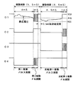
20はAND回路であり、駆動制御信号P3と駆動制御信号P4をインバータ21によって反転した信号を入力し、バイアス制御信号P14を出力する。22はバイアス回路であり、電源電圧の約1/2であるバイアス電圧P15を出力する。23はアナログスイッチであり、前記バイアス制御信号P14を制御端子Cに入力し、前記バイアス電圧P15を前記駆動パルスO2に供給又は遮断する機能を有する。24はAND回路であり、駆動制御信号P5と駆動制御信号P6をインバータ25によって反転した信号を入力し、バイアス制御信号P16を出力する。26はバイアス回路であり、電源電圧の約1/2であるバイアス電圧P17を出力する。27はアナログスイッチであり、前記バイアス制御信号P16を制御端子Cに入力し、前記バイアス電圧P17を前記駆動パルスO3に供給又は遮断する機能を有する。 An AND circuit 20 receives a drive control signal P3 and a signal obtained by inverting the drive control signal P4 by the inverter 21 and outputs a bias control signal P14. Reference numeral 22 denotes a bias circuit, which outputs a bias voltage P15 that is about ½ of the power supply voltage. An analog switch 23 has a function of inputting the bias control signal P14 to the control terminal C and supplying or blocking the bias voltage P15 to the drive pulse O2. An AND circuit 24 inputs a signal obtained by inverting the drive control signal P5 and the drive control signal P6 by the inverter 25, and outputs a bias control signal P16. A bias circuit 26 outputs a bias voltage P17 that is about ½ of the power supply voltage. An analog switch 27 has a function of inputting the bias control signal P16 to the control terminal C and supplying or cutting off the bias voltage P17 to the drive pulse O3.
次に図2で示した駆動手段としての駆動回路の動作と、可逆ステッピングモータ1のロータ2の正転方向の回転動作を図3に基づいて説明する。尚、説明を分かり易くするために、各動作をタイミングA〜タイミングFまでの6段階に分けて説明する。図3に於いて、タイミングAは無励磁状態であり、コイル6、7には駆動パルスが印加されず、駆動
パルスO1〜O4は共に論理“1”(VDD)であり、第1ステータ磁極部3、第2ステータ磁極部4、第3ステータ磁極部5は共に励磁されず、ロータ2は初期状態として図面上N極が上、S極が下の状態で停止している。ここで、制御回路11は駆動パルスO1〜O4を全て論理“1”とするために、全ての駆動制御信号P1〜P8を論理“0”として出力する。
Next, the operation of the drive circuit as the drive means shown in FIG. 2 and the rotation operation of the
次に、タイミングBはコイル7に対して第1駆動パルスが出力されるタイミングであり、制御回路11は駆動制御信号P5、P6を論理“0”とするので駆動パルスO3は論理“1”となり、更に制御回路11は駆動制御信号P7、P8を論理“1”とするので駆動パルスO4は論理“0”(VSS)とされて、コイル7のコイル端子7aからコイル端子7bに駆動電流が流れる。これにより、コイル7は駆動コイルとされて第2ステータ磁極部4はN極に励磁され、第1ステータ磁極部3と第3ステータ磁極部5はS極に励磁され、ロータ2は左方向(正転)に回転を開始し、90度以上回転する。ここで、第2ステータ磁極部4はロータ2のN極を引き離す方向に励磁され(すなわちN極に励磁)、また、第3ステータ磁極部5はロータ2のS極を引き離す方向に励磁される(すなわちS極に励磁)。
Next, timing B is the timing at which the first drive pulse is output to the
また、タイミングBに於いて、制御回路11は駆動制御信号P1を論理“1”、駆動制御信号P2を論理“0”とし、インバータ12のP−Tr12aとN−Tr12bを共にOFFして駆動パルスO1を高抵抗状態とする。同様に制御回路11は駆動制御信号P3を論理“1”、駆動制御信号P4を論理“0”とし、インバータ13のP−Tr13aとN−Tr13bを共にOFFして駆動パルスO2を高抵抗状態とする。ここで、AND回路20は駆動制御信号P3と駆動制御信号P4の反転出力を入力しているので、その出力であるバイアス制御信号P14は論理“1”となってアナログスイッチ23をONし、バイアス回路22の出力であるバイアス電圧P15を高抵抗状態となっている駆動パルスO2に供給して駆動パルスO2をバイアス電圧P15と同電位とする。すなわち、タイミングBに於いて、駆動パルスO2はバイアス電圧P15の電位に等しい約1/2VDDの電圧とされ、駆動パルスO1は高抵抗状態とされる。
At timing B, the control circuit 11 sets the drive control signal P1 to logic “1”, the drive control signal P2 to logic “0”, and turns off both the P-
ここで、駆動パルスO1、O2は前述の如く、コイル6のコイル端子6a、6bにそれぞれ接続されているので、コイル端子6aは高抵抗状態、コイル6bは約1/2VDDとなってコイル6は誘起電圧を検出する検出コイルとされる。すなわち、ロータ2が駆動コイルであるコイル7によって回転を始めると、ロータ2の回転によって生じる磁束の変化が第1ステータ磁極部3と第3ステータ磁極部5を介してコイル6に伝達され、この磁束の変化によって発生した誘起電圧がコイル6のコイル端子6aとコイル端子6bの間に現れる。ここで、前述した如く、コイル端子6bに接続されている駆動パルスO2はバイアス電圧P15と等しい電位(すなわち約1/2VDD)を有しているので、他方の端子であるコイル端子6aに接続されている駆動パルスO1には、駆動パルスO2の電位(すなわちバイアス電圧P15)を基準として誘起電圧が発生する。すなわち、該誘起電圧は、バイアス電圧P15の電位を中心に磁束の変化の方向に応じてプラス方向、又はマイナス方向に均等に発生するので、ダイナミックレンジの広い誘起電圧を得ることが出来る。
Here, since the drive pulses O1 and O2 are respectively connected to the
ここで、電圧検出回路16は駆動パルスO1を入力して誘起電圧を検出し、該誘起電圧が所定の電圧に達したならば、検出信号P9を出力する。AND回路18は、検出信号P9とマスク信号P11を入力して論理ANDを実行し、動的制御信号P12を出力する。制御回路11は動的制御信号P12を入力すると、タイミングBである第1駆動パルスを直ちに終了する。尚、電圧検出回路16が検出する所定の電圧は、バイアス電圧P15に略等しい電圧であることが好ましく、誘起電圧がバイアス電圧P15に達する付近で、ロータ2は初期の無励磁状態から約90度回転した位置となる。ここで第1駆動パルスの終了は、誘起電圧がバイアス電圧P15に達したときから若干遅れるので、ロータ2の回
転は初期状態から90度+αに達することになり、図3で示すタイミングBでのロータ2の回転位置は、タイミングBの終了時点での回転位置を示している。
Here, the voltage detection circuit 16 receives the drive pulse O1, detects the induced voltage, and outputs the detection signal P9 when the induced voltage reaches a predetermined voltage. The AND circuit 18 receives the detection signal P9 and the mask signal P11, performs a logical AND, and outputs a dynamic control signal P12. When the dynamic control signal P12 is input, the control circuit 11 immediately ends the first drive pulse at the timing B. The predetermined voltage detected by the voltage detection circuit 16 is preferably a voltage substantially equal to the bias voltage P15, and the
ここで例えば、モータの負荷が軽い場合、ロータ2は素早く回転するので、第1駆動パルスであるタイミングBが開始されてから誘起電圧がバイアス電圧P15に達するまでの時間は短くなり、この結果、第1駆動パルスの駆動時間は短く調整される。また、モータの負荷が重い場合、ロータ2はゆっくり回転するので、第1駆動パルスであるタイミングBが開始されてから誘起電圧がバイアス電圧P15に達するまでの時間は長くなり、この結果、第1駆動パルスの駆動時間は長く調整される。すなわち、第1駆動パルスのパルス幅は、制御回路11により誘起電圧が現すロータ2の回転角度に応じて動的制御される。尚、第1駆動パルスのパルス幅は、通常状態に於いて2mS〜4mSの範囲で制御されることが多い。
Here, for example, when the load on the motor is light, the
次に、タイミングCは第1駆動パルスの終了後、直ちに第2駆動パルスが出力されるタイミングであり、制御回路11は駆動制御信号P1、P2と駆動制御信号P7、P8を短時間に論理“1”と論理“0”を繰り返し、駆動パルスO1、O4を図示する如くチョッパ駆動する。また、制御回路11は、駆動制御信号P3、P4、P5、P6を論理“0”として出力し、駆動パルスO2、O3を論理“1”とする。これにより、コイル6のコイル端子6bからコイル端子6aに向かってチョッパ駆動電流が流れ、また同様に、コイル7のコイル端子7aからコイル端子7bに向かってチョッパ駆動電流が流れる。
Next, the timing C is a timing at which the second drive pulse is output immediately after the end of the first drive pulse, and the control circuit 11 outputs the drive control signals P1, P2 and the drive control signals P7, P8 in a short time. 1 "and logic" 0 "are repeated, and the drive pulses O1 and O4 are chopper driven as shown. Further, the control circuit 11 outputs the drive control signals P3, P4, P5, and P6 as logic “0”, and sets the drive pulses O2 and O3 to logic “1”. Thereby, a chopper driving current flows from the coil terminal 6b of the
この結果、二つのコイル6、コイル7は共に駆動コイルとして機能し、第1ステータ磁極部3と第2ステータ磁極部4はN極に励磁され、第3ステータ磁極部5はS極に励磁される。これにより、ロータ2のS極は第1ステータ磁極部3のN極によって引き寄せられ、また、ロータ2のN極は第1ステータ磁極部3のN極によって引き離されると共に第3ステータ磁極部5のS極によって引き寄せられるので、ロータ2は更に左方向(正転)に回転を継続して、タイミングAの無励磁の初期状態から1ステップ(すなわち180度)回転する。また、ロータ2が1ステップ回転すると、ロータ2のS極は第1ステータ磁極部3と第2ステータ磁極部4のN極によって両方から引き寄せられてブレーキがかかり、また、ロータ2のN極は第3ステータ磁極部5のS極に引き寄せられてブレーキがかかり、ロータ2は1ステップ回転したところで停止し安定する。
As a result, the two
次に、タイミングDの期間は再び無励磁の期間であり、駆動パルスO1〜O4は共に論理“1”とされ、コイル6と7には駆動電流が流れず、ロータ2は停止状態が継続される。例えば、可逆ステッピングモータが1秒間に1ステップ毎に駆動されているとすると、このタイミングDの期間は1秒からタイミングBとタイミングCの期間を差し引いた時間となる。
Next, the period of the timing D is a non-excitation period again, the drive pulses O1 to O4 are both set to logic “1”, the drive current does not flow through the
次に、ロータ2をタイミングDの位置から更に左方向(正転)に1ステップ回転させる動作を説明する。タイミングEはコイル7に対して反転第1駆動パルスが出力されるタイミングであり、制御回路11は駆動制御信号P5、P6を論理“1”とするので駆動パルスO3は論理“0”となり、更に制御回路11は駆動制御信号P7、P8を論理“0”とするので駆動パルスO4は論理“1”とされて、コイル7のコイル端子7bからコイル端子7aに駆動電流が流れる。これにより、コイル7は駆動コイルとされて第2ステータ磁極部4はS極に励磁され、第1ステータ磁極部3と第3ステータ磁極部5はN極に励磁され、ロータ2は再び左方向(正転)に回転を開始し、前記タイミングDの位置より90度以上回転する。ここで、第2ステータ磁極部4はロータ2のS極を引き離す方向に励磁され(すなわちS極に励磁)、また、第3ステータ磁極部5はロータ2のN極を引き離す方向に励磁される(すなわちN極に励磁)。
Next, the operation of rotating the
また、タイミングEに於いて、制御回路11は駆動制御信号P1を論理“1”、駆動制御信号P2を論理“0”とし、インバータ12のP−Tr12aとN−Tr12bを共にOFFして駆動パルスO1を高抵抗状態とする。同様に制御回路11は駆動制御信号P3を論理“1”、駆動制御信号P4を論理“0”とし、インバータ13のP−Tr13aとN−Tr13bを共にOFFして駆動パルスO2を高抵抗状態とする。ここで、AND回路20は駆動制御信号P3と駆動制御信号P4の反転出力を入力しているので、その出力であるバイアス制御信号P14は論理“1”となってアナログスイッチ23をONし、バイアス回路22の出力であるバイアス電圧P15を高抵抗状態となっている駆動パルスO2に供給して駆動パルスO2をバイアス電圧P15と同電位とする。すなわち、タイミングEに於いて、駆動パルスO2はバイアス電圧P15の電位に等しい約1/2VDDの電圧とされ、駆動パルスO1は高抵抗状態とされる。
At timing E, the control circuit 11 sets the drive control signal P1 to logic “1”, the drive control signal P2 to logic “0”, and turns off both the P-
ここで、駆動パルスO1、O2は前述の如く、コイル6のコイル端子6a、6bにそれぞれ接続されているので、コイル端子6aは高抵抗状態、コイル6bは約1/2VDDとなってコイル6は誘起電圧を検出する検出コイルとされる。すなわち、ロータ2が駆動コイルであるコイル7によって回転を始めると、ロータ2の回転によって生じる磁束の変化が第1ステータ磁極部3と第3ステータ磁極部5を介してコイル6に伝達され、この磁束の変化によって発生した誘起電圧がコイル6のコイル端子6aとコイル端子6bの間に現れる。ここで、前述した如く、コイル端子6bに接続されている駆動パルスO2はバイアス電圧P15と等しい電位(すなわち約1/2VDD)を有しているので、他方の端子であるコイル端子6aに接続されている駆動パルスO1には、駆動パルスO2の電位(すなわちバイアス電圧P15)を基準として誘起電圧が発生する。すなわち、該誘起電圧は、バイアス電圧P15の電位を中心に磁束の変化の方向に応じてプラス方向、又はマイナス方向に均等に発生するので、ダイナミックレンジの広い誘起電圧を得ることが出来る。尚、前記タイミングBに於いては、磁束の変化を起こすロータ2の磁極はN極であったが、タイミングEに於ける磁束の変化を起こすロータ2の磁極はS極であるので、図示するように誘起電圧の極性は反転し、誘起電圧はバイアス電圧P15を基準としてマイナス側に発生する。
Here, since the drive pulses O1 and O2 are respectively connected to the
ここで、電圧検出回路16は駆動パルスO1を入力して誘起電圧を検出し、該誘起電圧が所定の電圧に達したならば、検出信号P9を出力する。AND回路18は、検出信号P9とマスク信号P11を入力して論理ANDを実行し、動的制御信号P12を出力する。制御回路11は動的制御信号P12を入力すると、タイミングEである反転第1駆動パルスを直ちに終了する。尚、電圧検出回路16が検出する所定の電圧は、タイミングBと同様にバイアス電圧P15に略等しい電圧が好ましく、誘起電圧がバイアス電圧P15に達する付近で、ロータ2はタイミングDの無励磁状態から約90度回転した位置となる。ここで反転第1駆動パルスの終了は、誘起電圧がバイアス電圧P15に達したときから若干遅れるので、ロータ2の回転はタイミングDの位置から90度+αに達することになり、図3で示すタイミングEでのロータ2の回転位置は、タイミングEの終了時点での回転位置を示している。
Here, the voltage detection circuit 16 receives the drive pulse O1, detects the induced voltage, and outputs the detection signal P9 when the induced voltage reaches a predetermined voltage. The AND circuit 18 receives the detection signal P9 and the mask signal P11, performs a logical AND, and outputs a dynamic control signal P12. When receiving the dynamic control signal P12, the control circuit 11 immediately ends the inverted first drive pulse at the timing E. The predetermined voltage detected by the voltage detection circuit 16 is preferably a voltage substantially equal to the bias voltage P15 as in the case of the timing B, and the
ここで例えば、モータの負荷が軽い場合、ロータ2は素早く回転するので、反転第1駆動パルスであるタイミングEが開始されてから誘起電圧がバイアス電圧P15に達するまでの時間は短くなり、この結果、反転第1駆動パルスの駆動時間は短く調整される。また、モータの負荷が重い場合、ロータ2はゆっくり回転するので、反転第1駆動パルスであるタイミングEが開始されてから誘起電圧がバイアス電圧P15に達するまでの時間は長くなり、この結果、反転第1駆動パルスの駆動時間は長く調整される。すなわち、反転第1駆動パルスのパルス幅は、制御回路11により誘起電圧が現すロータ2の回転角度に応じて動的制御される。尚、反転第1駆動パルスのパルス幅は、前述の第1駆動パルスと同様に通常状態に於いて2mS〜4mSの範囲で制御されるが、図3に於いて、タイミン
グEの反転第1駆動パルスのパルス幅はタイミングBの第1駆動パルスより短く記しており、第1駆動パルス及び反転第1駆動パルスがモータの負荷変動等によって動的制御されることを示している。
Here, for example, when the load on the motor is light, the
次に、タイミングFは反転第1駆動パルスの終了後、直ちに反転第2駆動パルスが出力されるタイミングであり、制御回路11は駆動制御信号P3、P4と駆動制御信号P5、P6を短時間に論理“1”と論理“0”を繰り返し、駆動パルスO2、O3を図示する如くチョッパ駆動する。また、制御回路11は、駆動制御信号P1、P2、P7、P8を論理“0”として出力し、駆動パルスO1、O4を論理“1”とする。これにより、コイル6のコイル端子6aからコイル端子6bに向かってチョッパ駆動電流が流れ、また同様に、コイル7のコイル端子7bからコイル端子7aに向かってチョッパ駆動電流が流れる。
Next, timing F is a timing at which the inverted second drive pulse is output immediately after the end of the inverted first drive pulse, and the control circuit 11 sends the drive control signals P3 and P4 and the drive control signals P5 and P6 in a short time. The logic “1” and the logic “0” are repeated, and the drive pulses O2 and O3 are chopper driven as shown in the figure. Further, the control circuit 11 outputs the drive control signals P1, P2, P7, and P8 as logic “0”, and sets the drive pulses O1 and O4 to logic “1”. Thereby, a chopper drive current flows from the
この結果、二つのコイル6、コイル7は共に駆動コイルとして機能し、第1ステータ磁極部3と第2ステータ磁極部4はS極に励磁され、第3ステータ磁極部5はN極に励磁される。これにより、ロータ2のN極は第1ステータ磁極部3のS極によって引き寄せられ、また、ロータ2のS極は第1ステータ磁極部3のS極によって引き離されると共に第3ステータ磁極部5のN極によって引き寄せられるので、ロータ2は更に左方向(正転)に回転を継続して、タイミングDの無励磁状態から1ステップ(すなわち180度)回転する。また、ロータ2が1ステップ回転すると、ロータ2のN極は第1ステータ磁極部3と第2ステータ磁極部4のS極によって両方から引き寄せられてブレーキがかかり、また、ロータ2のS極は第3ステータ磁極部5のN極に引き寄せられてブレーキがかかり、ロータ2は1ステップ回転したところで停止し安定する。以上のように、タイミングA〜タイミングFまでを繰り返すことによってロータ2は2ステップ(すなわち360度)ずつ左方向(正転)に回転する。
As a result, the two
尚、タイミングBに於いて、前述した如く駆動コイルであるコイル7により、第2ステータ磁極部4はロータ2のN極を引き離す方向に励磁され、また、第3ステータ磁極部5はロータ2のS極を引き離す方向に励磁されるので、検出コイルであるコイル6はロータの発生する磁束を引き込む方向に配置されることになる。この結果、コイル6に発生する誘起電圧のレベルが上昇し誘起電圧の検出精度を向上させることが出来る。また同様に、タイミングEに於いても、前述した如く駆動コイルであるコイル7により、第2ステータ磁極部4はロータ2のS極を引き離す方向に励磁され、また、第3ステータ磁極部5はロータ2のN極を引き離す方向に励磁されるので、検出コイルであるコイル6はロータ2の発生する磁束を引き込む方向に配置されることになる。この結果、コイル6に発生する誘起電圧のレベルが上昇し誘起電圧の検出精度を向上させることが出来る。
At the timing B, the second stator
また、タイミングCによる第2駆動パルスとタイミングFによる反転第2駆動パルスの期間は通常1mS位であることが好ましく、またチョッパ周期は200μS〜250μS程度であることが好ましい。また、第2駆動パルス及び反転第2駆動パルスをチョッパ駆動とする理由は、第1駆動パルス及び反転第1駆動パルスよりも駆動エネルギーを小さくして、ロータ2に対する過度のブレーキ効果を無くし、ロータ2の回転動作をスムーズにさせるためである。また、第2駆動パルス及び反転第2駆動パルスの駆動エネルギーを調整するためにチョッパ波形のデューティを可変しても良い。また、第2駆動パルス及び反転第2駆動パルスはチョッパ駆動に限定されず、フル駆動パルスであっても良く、また、駆動エネルギーの調整のために、駆動電圧や駆動電流を調整しても良い。
The period of the second drive pulse at timing C and the inverted second drive pulse at timing F is preferably about 1 mS, and the chopper period is preferably about 200 μS to 250 μS. The reason why the second drive pulse and the inverted second drive pulse are chopper driven is that the drive energy is made smaller than that of the first drive pulse and the inverted first drive pulse, and the excessive braking effect on the
次に、可逆ステッピングモータ1のロータ2の逆転方向の回転動作を図4に基づいて説明する。尚、説明を分かり易くするために、前述の図3と同様に各動作をタイミングA〜タイミングFまでの6段階に分けて説明する。また、正転方向の回転動作を説明した図
3と重複する箇所は一部説明を省略する。図4に於いて、タイミングAは無励磁状態であり、コイル6、7には駆動パルスが印加されず、駆動パルスO1〜O4は共に論理“1”(VDD)であり、第1ステータ磁極部3、第2ステータ磁極部4、第3ステータ磁極部5は共に励磁されず、ロータ2は初期状態として図面上N極が上、S極が下の状態で停止している。
Next, the rotation operation of the
次に、タイミングBはコイル6に対して第1駆動パルスが出力されるタイミングであり、制御回路11は駆動制御信号P3、P4を論理“0”とするので駆動パルスO2は論理“1”となり、更に制御回路11は駆動制御信号P1、P2を論理“1”とするので駆動パルスO1は論理“0”(VSS)とされて、コイル6のコイル端子6bからコイル端子6aに駆動電流が流れる。これにより、コイル6は駆動コイルとされて第1ステータ磁極部3はN極に励磁され、第2ステータ磁極部4と第3ステータ磁極部5はS極に励磁され、ロータ2は右方向(逆転)に回転を開始し、90度以上回転する。ここで、第1ステータ磁極部3はロータ2のN極を引き離す方向に励磁され(すなわちN極に励磁)、また、第3ステータ磁極部5はロータ2のS極を引き離す方向に励磁される(すなわちS極に励磁)。
Next, timing B is the timing at which the first drive pulse is output to the
また、タイミングBに於いて、制御回路11は駆動制御信号P7を論理“1”、駆動制御信号P8を論理“0”とし、インバータ15のP−Tr15aとN−Tr15bを共にOFFして駆動パルスO4を高抵抗状態とする。同様に制御回路11は駆動制御信号P5を論理“1”、駆動制御信号P6を論理“0”とし、インバータ14のP−Tr14aとN−Tr14bを共にOFFして駆動パルスO3を高抵抗状態とする。ここで、AND回路24は駆動制御信号P5と駆動制御信号P6の反転出力を入力しているので、その出力であるバイアス制御信号P16は論理“1”となってアナログスイッチ27をONし、バイアス回路26の出力であるバイアス電圧P17を高抵抗状態となっている駆動パルスO3に供給して駆動パルスO3をバイアス電圧P17と同電位とする。すなわち、タイミングBに於いて、駆動パルスO3はバイアス電圧P17の電位に等しい約1/2VDDの電圧とされ、駆動パルスO4は高抵抗状態とされる。
At timing B, the control circuit 11 sets the drive control signal P7 to logic “1”, the drive control signal P8 to logic “0”, and turns off both the P-
ここで、駆動パルスO3、O4は前述の如く、コイル7のコイル端子7a、7bにそれぞれ接続されているので、コイル端子7bは高抵抗状態、コイル7aは約1/2VDDとなってコイル7は誘起電圧を検出する検出コイルとされる。すなわち、ロータ2が駆動コイルであるコイル6によって回転を始めると、ロータ2の回転によって生じる磁束の変化が第2ステータ磁極部4と第3ステータ磁極部5を介してコイル7に伝達され、この磁束の変化によって発生した誘起電圧がコイル7のコイル端子7aとコイル端子7bの間に現れる。ここで、前述した如く、コイル端子7aに接続されている駆動パルスO3はバイアス電圧P17と等しい電位(すなわち約1/2VDD)を有しているので、他方の端子であるコイル端子7bに接続されている駆動パルスO4には、駆動パルスO3の電位(すなわちバイアス電圧P17)を基準として誘起電圧が発生する。すなわち、該誘起電圧は、バイアス電圧P17の電位を中心に磁束の変化の方向に応じてプラス方向、又はマイナス方向に均等に発生するので、ダイナミックレンジの広い誘起電圧を得ることが出来る。
Here, since the drive pulses O3 and O4 are connected to the
ここで、電圧検出回路17は駆動パルスO4を入力して誘起電圧を検出し、該誘起電圧が所定の電圧に達したならば、検出信号P10を出力する。AND回路19は、検出信号P10とマスク信号P11を入力して論理ANDを実行し、動的制御信号P13を出力する。制御回路11は動的制御信号P13を入力すると、タイミングBである第1駆動パルスを直ちに終了する。尚、電圧検出回路17が検出する所定の電圧は、バイアス電圧P17に略等しい電圧であることが好ましく、誘起電圧がバイアス電圧P17に達する付近で、ロータ2は初期の無励磁状態から約90度回転した位置となる。ここで第1駆動パルスの終了は、誘起電圧がバイアス電圧P17に達したときから若干遅れるので、ロータ2
の回転は初期状態から90度+αに達することになり、図4で示すタイミングBでのロータ2の回転位置は、タイミングBの終了時点での回転位置を示している。
Here, the voltage detection circuit 17 receives the drive pulse O4, detects the induced voltage, and outputs the detection signal P10 when the induced voltage reaches a predetermined voltage. The AND circuit 19 receives the detection signal P10 and the mask signal P11, performs a logical AND, and outputs a dynamic control signal P13. When the dynamic control signal P13 is input, the control circuit 11 immediately ends the first drive pulse at the timing B. The predetermined voltage detected by the voltage detection circuit 17 is preferably a voltage substantially equal to the bias voltage P17, and the
4 reaches 90 ° + α from the initial state, and the rotational position of the
ここで例えば、モータの負荷が軽い場合、ロータ2は素早く回転するので、第1駆動パルスであるタイミングBが開始されてから誘起電圧がバイアス電圧P17に達するまでの時間は短くなり、この結果、第1駆動パルスの駆動時間は短く調整される。また、モータの負荷が重い場合、ロータ2はゆっくり回転するので、第1駆動パルスであるタイミングBが開始されてから誘起電圧がバイアス電圧P17に達するまでの時間は長くなり、この結果、第1駆動パルスの駆動時間は長く調整される。すなわち、第1駆動パルスのパルス幅は、制御回路11により誘起電圧が現すロータ2の回転角度に応じて動的制御される。尚、第1駆動パルスのパルス幅は、通常状態に於いて2mS〜4mSの範囲で制御されることが多い。
Here, for example, when the load on the motor is light, the
次に、タイミングCは第1駆動パルスの終了後、直ちに第2駆動パルスが出力されるタイミングであり、制御回路11は駆動制御信号P1、P2と駆動制御信号P7、P8を短時間に論理“1”と論理“0”を繰り返し、駆動パルスO1、O4を図示する如くチョッパ駆動する。また、制御回路11は、駆動制御信号P3、P4、P5、P6を論理“0”として出力し、駆動パルスO2、O3を論理“1”とする。これにより、コイル6のコイル端子6bからコイル端子6aに向かってチョッパ駆動電流が流れ、また同様に、コイル7のコイル端子7aからコイル端子7bに向かってチョッパ駆動電流が流れる。
Next, the timing C is a timing at which the second drive pulse is output immediately after the end of the first drive pulse, and the control circuit 11 outputs the drive control signals P1, P2 and the drive control signals P7, P8 in a short time. 1 "and logic" 0 "are repeated, and the drive pulses O1 and O4 are chopper driven as shown. Further, the control circuit 11 outputs the drive control signals P3, P4, P5, and P6 as logic “0”, and sets the drive pulses O2 and O3 to logic “1”. Thereby, a chopper driving current flows from the coil terminal 6b of the
この結果、二つのコイル6、コイル7は共に駆動コイルとして機能し、第1ステータ磁極部3と第2ステータ磁極部4はN極に励磁され、第3ステータ磁極部5はS極に励磁される。これにより、ロータ2のS極は第2ステータ磁極部4のN極によって引き寄せられ、また、ロータ2のN極は第2ステータ磁極部4のN極によって引き離されると共に第3ステータ磁極部5のS極によって引き寄せられるので、ロータ2は更に右方向(逆転)に回転を継続して、タイミングAの無励磁の初期状態から1ステップ(すなわち180度)回転する。また、ロータ2が1ステップ回転すると、ロータ2のS極は第1ステータ磁極部3と第2ステータ磁極部4のN極によって両方から引き寄せられてブレーキがかかり、また、ロータ2のN極は第3ステータ磁極部5のS極に引き寄せられてブレーキがかかり、ロータ2は1ステップ回転したところで停止し安定する。
As a result, the two
次に、タイミングDの期間は再び無励磁の期間であり、駆動パルスO1〜O4は共に論理“1”とされ、コイル6と7には駆動電流が流れず、ロータ2は停止状態が継続される。
Next, the period of the timing D is a non-excitation period again, the drive pulses O1 to O4 are both set to logic “1”, the drive current does not flow through the
次に、ロータ2をタイミングDの位置から更に右方向(逆転)に1ステップ回転させる動作を説明する。タイミングEはコイル6に対して反転第1駆動パルスが出力されるタイミングであり、制御回路11は駆動制御信号P3、P4を論理“1”とするので駆動パルスO2は論理“0”となり、更に制御回路11は駆動制御信号P1、P2を論理“0”とするので駆動パルスO1は論理“1”とされて、コイル6のコイル端子6aからコイル端子6bに駆動電流が流れる。これにより、コイル6は駆動コイルとされて第1ステータ磁極部3はS極に励磁され、第2ステータ磁極部4と第3ステータ磁極部5はN極に励磁され、ロータ2は再び右方向(逆転)に回転を開始し、前記タイミングDの位置より90度以上回転する。ここで、第1ステータ磁極部3はロータ2のS極を引き離す方向に励磁され(すなわちS極に励磁)、また、第3ステータ磁極部5はロータ2のN極を引き離す方向に励磁される(すなわちN極に励磁)。
Next, the operation of rotating the
また、タイミングEに於いて、制御回路11は駆動制御信号P7を論理“1”、駆動制御信号P8を論理“0”とし、インバータ15のP−Tr15aとN−Tr15bを共
にOFFして駆動パルスO4を高抵抗状態とする。同様に制御回路11は駆動制御信号P5を論理“1”、駆動制御信号P6を論理“0”とし、インバータ14のP−Tr14aとN−Tr14bを共にOFFして駆動パルスO3を高抵抗状態とする。ここで、AND回路24は駆動制御信号P5と駆動制御信号P6の反転出力を入力しているので、その出力であるバイアス制御信号P16は論理“1”となってアナログスイッチ27をONし、バイアス回路26の出力であるバイアス電圧P17を高抵抗状態となっている駆動パルスO3に供給して駆動パルスO3をバイアス電圧P17と同電位とする。すなわち、タイミングEに於いて、駆動パルスO3はバイアス電圧P17の電位に等しい約1/2VDDの電圧とされ、駆動パルスO4は高抵抗状態とされる。
At timing E, the control circuit 11 sets the drive control signal P7 to logic “1”, the drive control signal P8 to logic “0”, and turns off both the P-
ここで、駆動パルスO3、O4は前述の如く、コイル7のコイル端子7a、7bにそれぞれ接続されているので、コイル端子7bは高抵抗状態、コイル7aは約1/2VDDとなってコイル7は誘起電圧を検出する検出コイルとされる。すなわち、ロータ2が駆動コイルであるコイル6によって回転を始めると、ロータ2の回転によって生じる磁束の変化が第2ステータ磁極部4と第3ステータ磁極部5を介してコイル7に伝達され、この磁束の変化によって発生した誘起電圧がコイル7のコイル端子7aとコイル端子7bの間に現れる。ここで、前述した如く、コイル端子7aに接続されている駆動パルスO3はバイアス電圧P17と等しい電位(すなわち約1/2VDD)を有しているので、他方の端子であるコイル端子7bに接続されている駆動パルスO4には、駆動パルスO3の電位(すなわちバイアス電圧P17)を基準として誘起電圧が発生する。すなわち、該誘起電圧は、バイアス電圧P17の電位を中心に磁束の変化の方向に応じてプラス方向、又はマイナス方向に均等に発生するので、ダイナミックレンジの広い誘起電圧を得ることが出来る。尚、前記タイミングBに於いては、磁束の変化を起こすロータ2の磁極はN極であったが、タイミングEに於ける磁束の変化を起こすロータ2の磁極はS極であるので、図示するように誘起電圧の極性は反転し、誘起電圧はバイアス電圧P17を基準としてマイナス側に発生する。
Here, since the drive pulses O3 and O4 are connected to the
ここで、電圧検出回路17は駆動パルスO4を入力して誘起電圧を検出し、該誘起電圧が所定の電圧に達したならば、検出信号P10を出力する。AND回路19は、検出信号P10とマスク信号P11を入力して論理ANDを実行し、動的制御信号P13を出力する。制御回路11は動的制御信号P13を入力すると、タイミングEである反転第1駆動パルスを直ちに終了する。尚、電圧検出回路17が検出する所定の電圧は、タイミングBと同様にバイアス電圧P17に略等しい電圧が好ましく、誘起電圧がバイアス電圧P17に達する付近で、ロータ2はタイミングDの無励磁状態から約90度回転した位置となる。ここで反転第1駆動パルスの終了は、誘起電圧がバイアス電圧P17に達したときから若干遅れるので、ロータ2の回転はタイミングDの位置から90度+αに達することになり、図4で示すタイミングEでのロータ2の回転位置は、タイミングEの終了時点での回転位置を示している。
Here, the voltage detection circuit 17 receives the drive pulse O4, detects the induced voltage, and outputs the detection signal P10 when the induced voltage reaches a predetermined voltage. The AND circuit 19 receives the detection signal P10 and the mask signal P11, performs a logical AND, and outputs a dynamic control signal P13. When receiving the dynamic control signal P13, the control circuit 11 immediately ends the inverted first drive pulse that is the timing E. The predetermined voltage detected by the voltage detection circuit 17 is preferably a voltage substantially equal to the bias voltage P17 as in the timing B, and the
ここで例えば、モータの負荷が軽い場合、ロータ2は素早く回転するので、反転第1駆動パルスであるタイミングEが開始されてから誘起電圧がバイアス電圧P17に達するまでの時間は短くなり、この結果、反転第1駆動パルスの駆動時間は短く調整される。また、モータの負荷が重い場合、ロータ2はゆっくり回転するので、反転第1駆動パルスであるタイミングEが開始されてから誘起電圧がバイアス電圧P17に達するまでの時間は長くなり、この結果、反転第1駆動パルスの駆動時間は長く調整される。すなわち、反転第1駆動パルスのパルス幅は、制御回路11により誘起電圧が現すロータ2の回転角度に応じて動的制御される。尚、反転第1駆動パルスのパルス幅は、前述の第1駆動パルスと同様に通常状態に於いて2mS〜4mSの範囲で制御されるが、図4に於いて、タイミングEの反転第1駆動パルスのパルス幅はタイミングBの第1駆動パルスより短く記しており、第1駆動パルス及び反転第1駆動パルスがモータの負荷変動等によって動的制御され
ることを示している。
Here, for example, when the load on the motor is light, the
次に、タイミングFは反転第1駆動パルスの終了後、直ちに反転第2駆動パルスが出力されるタイミングであり、制御回路11は駆動制御信号P3、P4と駆動制御信号P5、P6を短時間に論理“1”と論理“0”を繰り返し、駆動パルスO2、O3を図示する如くチョッパ駆動する。また、制御回路11は、駆動制御信号P1、P2、P7、P8を論理“0”として出力し、駆動パルスO1、O4を論理“1”とする。これにより、コイル6のコイル端子6aからコイル端子6bに向かってチョッパ駆動電流が流れ、また同様に、コイル7のコイル端子7bからコイル端子7aに向かってチョッパ駆動電流が流れる。
Next, timing F is a timing at which the inverted second drive pulse is output immediately after the end of the inverted first drive pulse, and the control circuit 11 sends the drive control signals P3 and P4 and the drive control signals P5 and P6 in a short time. The logic “1” and the logic “0” are repeated, and the drive pulses O2 and O3 are chopper driven as shown in the figure. Further, the control circuit 11 outputs the drive control signals P1, P2, P7, and P8 as logic “0”, and sets the drive pulses O1 and O4 to logic “1”. Thereby, a chopper drive current flows from the
この結果、二つのコイル6、コイル7は共に駆動コイルとして機能し、第1ステータ磁極部3と第2ステータ磁極部4はS極に励磁され、第3ステータ磁極部5はN極に励磁される。これにより、ロータ2のN極は第2ステータ磁極部4のS極によって引き寄せられ、また、ロータ2のS極は第2ステータ磁極部4のS極によって引き離されると共に第3ステータ磁極部5のN極によって引き寄せられるので、ロータ2は更に右方向(逆転)に回転を継続して、タイミングDの無励磁状態から1ステップ(すなわち180度)回転する。また、ロータ2が1ステップ回転すると、ロータ2のN極は第1ステータ磁極部3と第2ステータ磁極部4のS極によって両方から引き寄せられてブレーキがかかり、また、ロータ2のS極は第3ステータ磁極部5のN極に引き寄せられてブレーキがかかり、ロータ2は1ステップ回転したところで停止し安定する。以上のように、タイミングA〜タイミングFまでを繰り返すことによってロータ2は2ステップ(すなわち360度)ずつ右方向(逆転)に回転する。
As a result, the two
尚、タイミングBに於いて、前述した如く駆動コイルであるコイル6により、第1ステータ磁極部3はロータ2のN極を引き離す方向に励磁され、また、第3ステータ磁極部5はロータ2のS極を引き離す方向に励磁されるので、検出コイルであるコイル7はロータの発生する磁束を引き込む方向に配置されることになる。この結果、コイル7に発生する誘起電圧のレベルが上昇し誘起電圧の検出精度を向上させることが出来る。また同様に、タイミングEに於いても、前述した如く駆動コイルであるコイル6により、第1ステータ磁極部3はロータ2のS極を引き離す方向に励磁され、また、第3ステータ磁極部5はロータ2のN極を引き離す方向に励磁されるので、検出コイルであるコイル7はロータの発生する磁束を引き込む方向に配置されることになる。この結果、コイル7に発生する誘起電圧のレベルが上昇し誘起電圧の検出精度を向上させることが出来る。
At timing B, as described above, the first stator
また、タイミングCによる第2駆動パルスとタイミングFによる反転第2駆動パルスの期間は通常1mS位であることが好ましく、またチョッパ周期は200μS〜250μS程度であることが好ましい。また、第2駆動パルス及び反転第2駆動パルスをチョッパ駆動とする理由等は、図3の正転動作で説明した内容と同様であるので省略する。 The period of the second drive pulse at timing C and the inverted second drive pulse at timing F is preferably about 1 mS, and the chopper period is preferably about 200 μS to 250 μS. The reason why the second drive pulse and the inverted second drive pulse are chopper-driven is the same as that described in the normal rotation operation of FIG.
次に図5に基づいて本発明の実施例1の可逆ステッピングモータの検出コイルに発生する誘起電圧と電圧検出手段の動作を説明する。説明の前提として、可逆ステッピングモータのロータ2が正転動作をしているときに発生する誘起電圧を基にして説明する。ここで、該誘起電圧は前述した如く、ロータ2の正転動作に於いて第1駆動パルスの期間に高抵抗状態とされた駆動パルスO1に発生する。電圧検出手段としての電圧検出回路16は、第1駆動パルスの期間を誘起電圧検出期間として前記駆動パルスO1を入力し、誘起電圧が所定の電圧としてのバイアス電圧P15に達するかどうかを判定する。そして該誘起電圧がバイアス電圧P15に達した場合(すなわち、ここではバイアス電圧P15以下となった場合)は、検出信号P9を出力する。尚、誘起電圧には外部などから図5に示すような電気的なノイズが発生することがあり、検出信号P9a、P9bは誘起電圧に発生した
ノイズを検出した結果であり、また、検出信号P9cは誘起電圧がバイアス電圧P15以下となったことを検出した正しい検出信号である。
Next, the induced voltage generated in the detection coil of the reversible stepping motor according to the first embodiment of the present invention and the operation of the voltage detection means will be described with reference to FIG. As a premise for explanation, explanation will be made based on the induced voltage generated when the
ここで、ノイズによって検出された検出信号P9a、P9bがそのまま制御回路11に入力されると、制御回路11は検出信号P9a、又は検出信号P9bによって誘起電圧が所定の電圧に達したと誤認識して第1駆動パルスを終了させてしまい、結果として、ロータ2の回転が停止してしまう等の危険性がある。このような誘起電圧に発生するノイズの影響を最小限に抑えるために、本実施例では電圧検出回路16の後にAND回路18によるマスク回路を備え、電圧検出回路16の誘起電圧検出期間に所定のマスク期間を設ける対策を実施している。
Here, when the detection signals P9a and P9b detected by noise are input to the control circuit 11 as they are, the control circuit 11 erroneously recognizes that the induced voltage has reached a predetermined voltage by the detection signal P9a or the detection signal P9b. Thus, there is a risk that the first drive pulse is ended and, as a result, the rotation of the
すなわち、図5に示すように、マスク信号P11は第1駆動パルスの期間の開始に同期して論理“0”となり、第1駆動パルス期間の途中で論理“1”に戻る信号である。検出信号P9は、このマスク信号P11とAND回路18によって論理ANDされるので、マスク信号P11が論理“0”期間、すなわち、マスク期間に於いては、誘起電圧のノイズによって検出信号P9が発生しても、AND回路18の出力である動的制御信号P12には図示するようにノイズによる動的制御信号P12はマスクされて出力されず、マスク信号P11が論理“1”とされた期間に発生した検出信号P9cが動的制御信号P12cとして制御回路11に入力される。このように、本発明に於いては電圧検出回路16の誘起電圧検出期間中にマスク期間を設けることが出来るので、マスク期間内に誘起電圧に発生する電気的ノイズによる誤動作を防止し、駆動パルスの動的制御の信頼性を向上させることが出来る。 That is, as shown in FIG. 5, the mask signal P11 is a signal that becomes logic “0” in synchronization with the start of the first drive pulse period and returns to logic “1” in the middle of the first drive pulse period. Since the detection signal P9 is logically ANDed with the mask signal P11 by the AND circuit 18, the detection signal P9 is generated by noise of the induced voltage during the logic “0” period, that is, the mask period. However, the dynamic control signal P12 due to noise is not masked and output to the dynamic control signal P12 which is the output of the AND circuit 18, and is generated during the period when the mask signal P11 is set to logic "1". The detected signal P9c is input to the control circuit 11 as the dynamic control signal P12c. Thus, in the present invention, since the mask period can be provided during the induced voltage detection period of the voltage detection circuit 16, malfunction due to electrical noise generated in the induced voltage within the mask period is prevented, and the drive pulse The reliability of dynamic control can be improved.
また、前述した如く、電圧検出回路16はヒステリシス回路16aを内蔵し、誘起電圧の検出にヒステリシス特性を設けている。すなわち、該ヒステリシス回路16aは電圧ヒステリシス手段として機能し、図5で示すように誘起電圧がバイアス電圧P15から更にヒステリシス電圧分下がったときに、検出信号P9を出力する。これにより、例えば誘起電圧に振幅の小さなノイズ成分が重畳されているような場合、ノイズによる検出信号P9の誤動作を防止し、駆動パルスの動的制御の信頼性を向上させることが出来る。尚、ヒステリシス電圧は電源電圧に対して1%〜10%の範囲であることが好ましい。また、ヒステリシス回路16aは誘起電圧がバイアス電圧P15に達してから一定時間経過後に検出信号P9を出力する時間ヒステリシス手段として機能しても良い。 As described above, the voltage detection circuit 16 has a built-in hysteresis circuit 16a and provides hysteresis characteristics for detecting the induced voltage. That is, the hysteresis circuit 16a functions as a voltage hysteresis means, and outputs a detection signal P9 when the induced voltage is further lowered from the bias voltage P15 by the hysteresis voltage as shown in FIG. Thereby, for example, when a noise component having a small amplitude is superimposed on the induced voltage, it is possible to prevent malfunction of the detection signal P9 due to noise and improve the reliability of dynamic control of the drive pulse. The hysteresis voltage is preferably in the range of 1% to 10% with respect to the power supply voltage. The hysteresis circuit 16a may function as time hysteresis means for outputting the detection signal P9 after a lapse of a fixed time after the induced voltage reaches the bias voltage P15.
すなわち、誘起電圧がバイアス電圧P15以下になってから一定時間の経過内で誘起電圧がバイアス電圧P15以下を継続したときに、検出信号P9を出力させる機能を用いても良い。尚、動的制御信号P12が出力されると、制御回路11は直ちに第1駆動パルスの期間を終了し第2駆動パルスの期間に移行するが、以降の動作の説明は重複するので省略する。また、図5での説明は、ロータ2が正転動作していることを前提に説明したが、逆転動作に於いては、誘起電圧が駆動パルスO4に発生することを除けば、他の基本動作は同じであるので説明は省略する。
That is, a function of outputting the detection signal P9 when the induced voltage continues below the bias voltage P15 within a predetermined time after the induced voltage becomes equal to or less than the bias voltage P15 may be used. When the dynamic control signal P12 is output, the control circuit 11 immediately ends the period of the first drive pulse and shifts to the period of the second drive pulse. The description in FIG. 5 is based on the assumption that the
次に図6に基づいて本発明の実施例1の可逆ステッピングモータの第1駆動パルスの別形態を説明する。説明の前提として、可逆ステッピングモータのロータ2が正転動作をしているときの第1駆動パルスの形態を説明する。図6に於いて、駆動パルスO1には、第1駆動パルスの期間、図示するように誘起電圧が発生する。マスク信号P11は、第1駆動パルスの期間の開始に同期して論理“0”となり、所定の時間後、論理“1”に戻る信号である。そして、マスク信号P11が論理“0”の期間が前述した如く、誘起電圧の検出をマスクする期間である。駆動パルスO4は、前記マスク信号P11によるマスク期間に同期して論理“1”と論理“0”を一定周期で繰り返すチョッパ駆動期間を有し、マスク信号P11のマスク期間の終了に合わせて論理“0”が継続するフル駆動パルス期間
となる。
Next, another form of the first drive pulse of the reversible stepping motor according to the first embodiment of the present invention will be described with reference to FIG. As a premise for explanation, the form of the first drive pulse when the
すなわち、第1駆動パルスのチョッパ駆動期間に於いては、駆動パルスO3、O4が接続されているコイル7のコイル端子7aからコイル端子7bに向かってチョッパ駆動電流が流れ、また、第1駆動パルスのフル駆動パルス期間に於いては、同様に駆動パルスO3、O4が接続されているコイル7のコイル端子7aからコイル端子7bに向かってフル駆動電流が流れる。ここで、チョッパ駆動期間中に於いては、駆動パルスO1に発生する誘起電圧には、コイル7に流れるチョッパ駆動電流の影響で、図示するようなノイズ成分が重畳される可能性があるが、チョッパ駆動期間は、前述の如く、マスク信号P11によるマスク期間でもあるので、ノイズ成分はマスク信号P11によってマスクされ、駆動パルスの動的制御は誤動作せず信頼性は維持される。
That is, during the chopper driving period of the first driving pulse, a chopper driving current flows from the
またこのように、第1駆動パルスの一部をチョッパ駆動する理由は、駆動コイルに流れる駆動電流の一部をチョッパ駆動電流とすることにより、モータ駆動の低消費電力を実現出来るからである。また、マスク期間以外の期間に於いて第1駆動パルスをフル駆動パルス期間とする理由は、フル駆動パルスでの駆動電流は直流電流に近いためにノイズ成分が発生し難く、誘起電圧にノイズが重畳されないので電圧検出回路16の誤動作を防ぐことが出来るからである。また、図6での説明は、ロータ2が正転動作していることを前提に説明したが、逆転動作に於いては、誘起電圧が駆動パルスO4に発生し、駆動パルスO1がチョッパ駆動となることを除けば、他の基本動作は同じであるので説明は省略する。
In addition, the reason why a part of the first drive pulse is chopper-driven is that a part of the drive current flowing in the drive coil is used as a chopper drive current, thereby realizing low power consumption for motor drive. In addition, the reason why the first drive pulse is set to the full drive pulse period in the period other than the mask period is that the drive current in the full drive pulse is close to the direct current, so that it is difficult to generate a noise component, and the induced voltage has noise. This is because the voltage detection circuit 16 can be prevented from malfunctioning because it is not superimposed. The description in FIG. 6 is based on the assumption that the
次に図7に基づいて本発明の実施例1の可逆ステッピングモータの高速駆動動作を説明する。尚、高速駆動動作とは1ステップの駆動周期が非常に短い(例えば10mS以下等)駆動動作を言い、また、説明の前提として、1ステップの駆動周期が固定である固定駆動周期方式の高速駆動動作であり、且つ、ロータ2の回転方向が正転動作であるとする。図7に於いて、駆動パルスO1〜O4は、図3で前述した駆動動作に準じた動作を行っており、フル駆動パルスによる第1駆動パルス期間、その次にチョッパ駆動による第2駆動パルス期間、その次にフル駆動パルスによる反転第1駆動パルス期間、更にその次にチョッパ駆動による反転第2駆動パルス期間と動作が継続する。
Next, the high-speed driving operation of the reversible stepping motor according to the first embodiment of the present invention will be described with reference to FIG. The high-speed driving operation refers to a driving operation in which the driving cycle of one step is very short (for example, 10 mS or less), and as a premise for explanation, the high-speed driving of the fixed driving cycle method in which the driving cycle of one step is fixed. It is an operation, and the rotation direction of the
ここで前述した如く、1ステップの駆動周期は固定であり、その駆動周期は一例として5.5mSであるとする。ここで、図示するように第1駆動パルスの期間が4mS経過した時点で駆動パルスO1に発生する誘起電圧がバイアス電圧P15に達するので直ちに第1駆動パルスの期間は終了し、第2駆動パルス期間が開始される。第2駆動パルス期間が1mSの固定であるとすれば、第1駆動パルスと第2駆動パルスの合計期間は4mS+1mS=5mSである。ここで、駆動周期は5.5mSであるので、駆動周期−(第1駆動パルス期間+第2駆動パルス期間)=0.5mSとなり、図示するように第2駆動パルス終了後に0.5mSの無励磁期間が存在し、駆動周期の固定が維持される。次に反転第1パルス期間では、何らかの原因によりモータ負荷が重くなりロータ2の回転が遅いために、反転パルス期間が4.5mSを経過しても誘起電圧がバイアス電圧P15に達しない状態を示している。
Here, as described above, the driving cycle of one step is fixed, and the driving cycle is assumed to be 5.5 mS as an example. Here, as shown in the figure, since the induced voltage generated in the drive pulse O1 reaches the bias voltage P15 when the period of the first drive pulse has passed 4 mS, the first drive pulse period ends immediately, and the second drive pulse period Is started. If the second drive pulse period is fixed at 1 mS, the total period of the first drive pulse and the second drive pulse is 4 mS + 1 mS = 5 mS. Here, since the driving period is 5.5 mS, the driving period− (first driving pulse period + second driving pulse period) = 0.5 mS, and, as shown in the drawing, 0.5 mS is not present after the end of the second driving pulse. There is an excitation period, and the fixed driving cycle is maintained. Next, in the first inversion pulse period, the motor load becomes heavy for some reason and the rotation of the
ここで、前述した如く、1ステップの駆動周期は5.5mSと決められているので、第2パルス幅が1mSの固定であるならば、反転第1駆動パルス幅の最大値は、5.5mS−1mS=4.5mSとなり、反転第1駆動パルス幅は、この最大値である4.5mSまで確保される。すなわち、駆動パルスの駆動周期が固定周期である場合は、第1駆動パルス(又は反転第1駆動パルス)は駆動周期と第2駆動パルス(又は反転第2駆動パルス)の幅の差まで確保されることになり、第1駆動パルス(又は反転第1駆動パルス)のパルス幅がそれ以上延長されることはない。但し、高速駆動は固定駆動周期方式に限定されるものではなく、第1駆動パルス(又は反転第1駆動パルス)に発生する誘起電圧がバイ
アス電圧P15に達するまで第1駆動パルス(又は反転第1駆動パルス)のパルス幅を延長し、駆動周期を可変とする可変駆動周期方式であっても良い。
Here, as described above, since the driving cycle of one step is determined to be 5.5 mS, if the second pulse width is fixed at 1 mS, the maximum value of the inverted first driving pulse width is 5.5 mS. −1 mS = 4.5 mS, and the inverted first drive pulse width is ensured up to the maximum value of 4.5 mS. That is, when the drive cycle of the drive pulse is a fixed cycle, the first drive pulse (or inverted first drive pulse) is secured up to the difference between the width of the drive cycle and the second drive pulse (or inverted second drive pulse). Thus, the pulse width of the first drive pulse (or the inverted first drive pulse) is not further extended. However, the high-speed driving is not limited to the fixed driving cycle method, and the first driving pulse (or the inverted first driving pulse) until the induced voltage generated in the first driving pulse (or the inverted first driving pulse) reaches the bias voltage P15. A variable drive cycle method in which the pulse width of the drive pulse) is extended and the drive cycle is variable may be used.
また、第1駆動パルス(又は反転第1駆動パルス)のパルス幅の延長を誘起電圧がバイアス電圧に達するまでではなく、所定の時間を限度として延長する時間制限付き可変駆動周期方式であっても良い。ここで、高速駆動に於ける各駆動方式をまとめると、図7で示した固定駆動周期方式は、第1駆動パルスのパルス幅を駆動パルスの駆動周期で決まる最大パルス幅まで確保するので、負荷変動等の外乱に対して信頼性の高い可逆ステッピングモータを提供出来る。更に、高速駆動のステップ送りを常に一定に送ることが出来る大きな効果があるが、モータの負荷変動や電源電圧等に比較的大きな変動が生じた場合、第1駆動パルスが強制的に終了されるので駆動トルクに余裕が無くなる可能性がある。 In addition, the variable drive cycle method with a time limit that extends the pulse width of the first drive pulse (or the inverted first drive pulse) not until the induced voltage reaches the bias voltage but for a predetermined time as a limit. good. Here, to summarize each driving method in the high-speed driving, the fixed driving cycle method shown in FIG. 7 secures the pulse width of the first driving pulse up to the maximum pulse width determined by the driving cycle of the driving pulse. A reversible stepping motor with high reliability against disturbances such as fluctuations can be provided. Furthermore, there is a great effect that the high-speed driving step feed can always be sent constantly. However, when a relatively large fluctuation occurs in the load fluctuation of the motor or the power supply voltage, the first driving pulse is forcibly terminated. Therefore, there is a possibility that there is no margin in drive torque.
また、可変駆動周期方式は、モータの負荷変動や電源電圧の変動に対して駆動周期を可変し、必要な駆動トルクを確保出来るので極めて信頼性の高いモータ駆動を実現出来る。また、該可変駆動周期方式に於いては、電源電圧が十分に高い場合は駆動トルクが大きいので第1駆動パルス幅は短くなり、これに準じて駆動周期も短くなる。また、電源電圧が低い場合は駆動トルクが小さいので第1駆動パルス幅は長くなって駆動トルクを確保し、これに準じて駆動周期も長くなる。従って可変駆動周期方式では、モータの負荷変動や電源電圧等の変動に応じて駆動周期が変化するので、常に一定の高速駆動を行うことは出来ない。 In addition, the variable drive cycle method can change the drive cycle in response to motor load fluctuations and power supply voltage fluctuations, and can secure the necessary drive torque, thereby realizing highly reliable motor drive. In the variable drive cycle method, when the power supply voltage is sufficiently high, the drive torque is large, so the first drive pulse width is shortened, and the drive cycle is shortened accordingly. In addition, when the power supply voltage is low, the driving torque is small, so the first driving pulse width is increased to ensure the driving torque, and the driving cycle is increased accordingly. Therefore, in the variable drive cycle method, the drive cycle changes in accordance with fluctuations in the motor load, power supply voltage, etc., so constant constant high-speed driving cannot be performed.
また、時間制限付き可変駆動周期方式は、固定駆動周期方式と可変駆動周期方式の中間的な方式であり、モータの負荷変動や電源電圧等の変動に対して必要な駆動トルクをある程度確保出来ると共に、モータの負荷変動や電源電圧の変動に対する駆動周期の変化に制限をつけて可変量を抑制することが出来る。このように、各駆動方式は、それぞれ効果に特徴があるので可逆ステッピングモータの仕様を考慮して各方式を選択すれば良い。尚、図7はロータ2の正転動作を前提として説明したが、ロータ2の逆転動作に於いても同様であり、その説明は省略する。以上のように本発明の実施例1によるならば、モータの負荷変動、電源電圧変動等の外乱に対して駆動パルスを動的制御し必要な駆動トルクを調整出来るので、安定したモータ駆動を実現する可逆ステッピングモータを提供することが出来る。また、モータ駆動の低消費電力化を可能とし、高速駆動にも十分対応出来るので、様々な用途に適した信頼性の高い可逆ステッピングモータを実現出来る。
The variable drive cycle method with time limit is an intermediate method between the fixed drive cycle method and the variable drive cycle method, and it can secure a certain amount of drive torque required for fluctuations in motor load and power supply voltage. The variable amount can be suppressed by limiting the change of the driving cycle with respect to the motor load fluctuation or the power supply voltage fluctuation. As described above, each driving method has a characteristic effect. Therefore, each method may be selected in consideration of the specifications of the reversible stepping motor. Note that FIG. 7 has been described on the assumption that the
次に図8に基づいて本発明の実施例2としての可逆ステッピングモータの正転駆動方式について説明する。実施例2の駆動方式は、駆動パルスが第1駆動パルスと第2駆動パルスと第3駆動パルスによって成ることを特徴とする。尚、説明を分かり易くするために、各動作をタイミングG〜タイミングNまでの8段階に分けて説明する。また、実施例2の可逆ステッピングモータと駆動回路は実施例1と同様であるので説明は省略し、可逆ステッピングモータの構成は図1を参照し、駆動回路の回路ブロック図は図2を参照する。図8に於いて、タイミングGは無励磁状態であり、実施例1の図3で述べたタイミングAと同様であるので説明は省略する。次にタイミングHはコイル7に対して第1駆動パルスが出力されるタイミングであり、コイル7に駆動電流が流れてロータ2は図示するように左方向(正転)に回転を開始するが、駆動パルスの形態及びロータ2の回転動作は実施例1の図3で述べたタイミングBと同様であるので詳細な説明は省略する。
Next, a normal rotation driving method of the reversible stepping motor according to the second embodiment of the present invention will be described with reference to FIG. The driving method of the second embodiment is characterized in that the driving pulse is composed of a first driving pulse, a second driving pulse, and a third driving pulse. For easy understanding, each operation will be described in 8 stages from timing G to timing N. Further, the reversible stepping motor and the drive circuit of the second embodiment are the same as those of the first embodiment, so that the description thereof will be omitted. Refer to FIG. 1 for the configuration of the reversible stepping motor, and refer to FIG. . In FIG. 8, the timing G is a non-excited state, which is the same as the timing A described in FIG. Next, timing H is a timing at which the first drive pulse is output to the
次に、タイミングIは第1駆動パルスの終了後、直ちに第2駆動パルスが出力されるタイミングであり、制御回路11は駆動制御信号P1〜P8をそれぞれ出力して駆動パルスO1、O3を論理“0”とし、駆動パルスO2、O4を論理“1”とする。これにより、コイル6のコイル端子6bからコイル端子6aに向かって駆動電流が流れ、また、コイ
ル7のコイル端子7bからコイル端子7aに向かって駆動電流が流れる。この結果、二つのコイル6、コイル7は共に駆動コイルとして機能し、第1ステータ磁極部3はN極に励磁され、第2ステータ磁極部4はS極に励磁され、第3ステータ磁極部5はS極とN極が打ち消し合って無励磁となる。これにより、ロータ2のN極は第1ステータ磁極部3のN極によって引き離され、また、ロータ2のS極は第2ステータ磁極部4のS極によって引き離されるので、ロータ2は更に左方向(正転)に回転を継続する。尚、タイミングIでの第2駆動パルスのパルス幅は固定であり、1mS程度が好ましい。
Next, the timing I is the timing at which the second drive pulse is output immediately after the end of the first drive pulse. The control circuit 11 outputs the drive control signals P1 to P8, respectively, and sets the drive pulses O1 and O3 to logic “ 0 "and drive pulses O2 and O4 are set to logic" 1 ". Thereby, a drive current flows from the coil terminal 6b of the
次に、タイミングJは第2駆動パルスの終了後、直ちに第3駆動パルスが出力されるタイミングであり、制御回路11は駆動制御信号P1〜P8をそれぞれ出力して駆動パルスO1、O4を論理“0”とし、駆動パルスO2、O3を論理“1”とする。これにより、コイル6のコイル端子6bからコイル端子6aに向かって駆動電流が継続して流れ、また、コイル7のコイル端子7aからコイル端子7bに向かって駆動電流が流れる。この結果、二つのコイル6、コイル7は共に駆動コイルとして機能し、第1ステータ磁極部3と第2ステータ磁極部4はN極に励磁され、第3ステータ磁極部5はS極に励磁される。これにより、ロータ2のS極は第1ステータ磁極部3と第2ステータ磁極部4のN極によって両方から引き寄せられてブレーキがかかり、また、ロータ2のN極は第3ステータ磁極部5のS極に引き寄せられてブレーキがかかり、ロータ2は1ステップ(すなわち180度)回転したところで停止し安定する。尚、タイミングJでの第3駆動パルスのパルス幅は固定であり、1mS程度が好ましい。
Next, timing J is the timing at which the third drive pulse is output immediately after the end of the second drive pulse, and the control circuit 11 outputs the drive control signals P1 to P8, respectively, and sets the drive pulses O1 and O4 to logic “ 0 "and drive pulses O2 and O3 are set to logic" 1 ". Thereby, a drive current flows continuously from the coil terminal 6b of the
次に、タイミングKの期間は再び無励磁の期間であり、駆動パルスO1〜O4は共に論理“1”とされ、コイル6と7には駆動電流が流れず、ロータ2は停止状態が継続される。次にタイミングLはコイル7に対して反転第1駆動パルスが出力されるタイミングであり、コイル7に反転した駆動電流が流れてロータ2は図示するように再び左方向(正転)に回転を開始するが、駆動パルスの形態及びロータ2の回転動作は実施例1の図3で述べたタイミングEと同様であるので詳細な説明は省略する。
Next, the period of the timing K is again a non-excitation period, the drive pulses O1 to O4 are both set to logic “1”, the drive current does not flow through the
次に、タイミングMは反転第1駆動パルスの終了後、直ちに反転第2駆動パルスが出力されるタイミングであり、制御回路11は駆動制御信号P1〜P8をそれぞれ出力して駆動パルスO2、O4を論理“0”とし、駆動パルスO1、O3を論理“1”とする。これにより、コイル6のコイル端子6aからコイル端子6bに向かって駆動電流が流れ、また、コイル7のコイル端子7aからコイル端子7bに向かって駆動電流が流れる。この結果、二つのコイル6、コイル7は共に駆動コイルとして機能し、第1ステータ磁極部3はS極に励磁され、第2ステータ磁極部4はN極に励磁され、第3ステータ磁極部5はS極とN極が打ち消し合って無励磁となる。これにより、ロータ2のS極は第1ステータ磁極部3のS極によって引き離され、また、ロータ2のN極は第2ステータ磁極部4のN極によって引き離されるので、ロータ2は更に左方向(正転)に回転を継続する。尚、タイミングMでの反転第2駆動パルスのパルス幅は固定であり、1mS程度が好ましい。
Next, timing M is a timing at which the inverted second drive pulse is output immediately after the end of the inverted first drive pulse, and the control circuit 11 outputs the drive control signals P1 to P8 respectively to generate the drive pulses O2 and O4. The logic is “0”, and the drive pulses O1 and O3 are logic “1”. Thereby, a drive current flows from the
次に、タイミングNは反転第2駆動パルスの終了後、直ちに反転第3駆動パルスが出力されるタイミングであり、制御回路11は駆動制御信号P1〜P8をそれぞれ出力して駆動パルスO2、O3を論理“0”とし、駆動パルスO1、O4を論理“1”とする。これにより、コイル6のコイル端子6aからコイル端子6bに向かって駆動電流が継続して流れ、また、コイル7のコイル端子7bからコイル端子7aに向かって駆動電流が流れる。この結果、二つのコイル6、コイル7は共に駆動コイルとして機能し、第1ステータ磁極部3と第2ステータ磁極部4はS極に励磁され、第3ステータ磁極部5はN極に励磁される。これにより、ロータ2のN極は第1ステータ磁極部3と第2ステータ磁極部4のS極によって両方から引き寄せられてブレーキがかかり、また、ロータ2のS極は第3ステータ磁極部5のN極に引き寄せられてブレーキがかかり、ロータ2は1ステップ(すなわ
ち180度)回転したところで停止し安定する。尚、タイミングNでの反転第3駆動パルスのパルス幅は固定であり、1mS程度が好ましい。
Next, the timing N is a timing at which the inverted third drive pulse is output immediately after the end of the inverted second drive pulse, and the control circuit 11 outputs the drive control signals P1 to P8 to output the drive pulses O2 and O3, respectively. The logic is “0”, and the drive pulses O1 and O4 are logic “1”. Thereby, a drive current flows continuously from the
次に図9に基づいて本発明の実施例2としての可逆ステッピングモータの逆転駆動方式について説明する。尚、逆転駆動方式は前述した図8での正転駆動方式に対し、駆動パルスO1と駆動パルスO4、及び駆動パルスO2と駆動パルスO3が入れ替わった動作であるので、一部重複する説明は省略する。図9に於いて、タイミングGは無励磁状態であり、実施例1の図4で述べたタイミングAと同様であるので説明は省略する。次にタイミングHはコイル6に対して第1駆動パルスが出力されるタイミングであり、コイル6に駆動電流が流れてロータ2は図示するように右方向(逆転)に回転を開始するが、駆動パルスの形態及びロータ2の回転動作は実施例1の図4で述べたタイミングBと同様であるので詳細な説明は省略する。
Next, the reverse drive system of the reversible stepping motor according to the second embodiment of the present invention will be described with reference to FIG. Note that the reverse drive method is an operation in which the drive pulse O1 and the drive pulse O4 and the drive pulse O2 and the drive pulse O3 are switched with respect to the forward drive method in FIG. To do. In FIG. 9, the timing G is a non-excited state, which is the same as the timing A described in FIG. Next, the timing H is a timing at which the first drive pulse is output to the
次に、タイミングIは第1駆動パルスの終了後、直ちに第2駆動パルスが出力されるタイミングであり、制御回路11は駆動制御信号P1〜P8をそれぞれ出力して駆動パルスO2、O4を論理“0”とし、駆動パルスO1、O3を論理“1”とする。これにより、コイル6のコイル端子6aからコイル端子6bに向かって駆動電流が流れ、また、コイル7のコイル端子7aからコイル端子7bに向かって駆動電流が流れる。この結果、二つのコイル6、コイル7は共に駆動コイルとして機能し、第1ステータ磁極部3はS極に励磁され、第2ステータ磁極部4はN極に励磁され、第3ステータ磁極部5はS極とN極が打ち消し合って無励磁となる。これにより、ロータ2のS極は第1ステータ磁極部3のS極によって引き離され、また、ロータ2のN極は第2ステータ磁極部4のN極によって引き離されるので、ロータ2は更に右方向(逆転)に回転を継続する。
Next, the timing I is a timing at which the second drive pulse is output immediately after the end of the first drive pulse. The control circuit 11 outputs the drive control signals P1 to P8, respectively, and sets the drive pulses O2 and O4 to logic “ 0 "and the drive pulses O1 and O3 are set to logic" 1 ". Thereby, a drive current flows from the
次に、タイミングJは第2駆動パルスの終了後、直ちに第3駆動パルスが出力されるタイミングであり、制御回路11は駆動制御信号P1〜P8をそれぞれ出力して駆動パルスO1、O4を論理“0”とし、駆動パルスO2、O3を論理“1”とする。これにより、コイル6のコイル端子6bからコイル端子6aに向かって駆動電流が流れ、また、コイル7のコイル端子7aからコイル端子7bに向かって駆動電流が継続して流れる。この結果、二つのコイル6、コイル7は共に駆動コイルとして機能し、第1ステータ磁極部3と第2ステータ磁極部4はN極に励磁され、第3ステータ磁極部5はS極に励磁される。これにより、ロータ2のS極は第1ステータ磁極部3と第2ステータ磁極部4のN極によって両方から引き寄せられてブレーキがかかり、また、ロータ2のN極は第3ステータ磁極部5のS極に引き寄せられてブレーキがかかり、ロータ2は1ステップ(すなわち180度)回転したところで停止し安定する。
Next, timing J is the timing at which the third drive pulse is output immediately after the end of the second drive pulse, and the control circuit 11 outputs the drive control signals P1 to P8, respectively, and sets the drive pulses O1 and O4 to logic “ 0 "and drive pulses O2 and O3 are set to logic" 1 ". Thereby, a drive current flows from the coil terminal 6b of the
次に、タイミングKの期間は再び無励磁の期間であり、駆動パルスO1〜O4は共に論理“1”とされ、コイル6と7には駆動電流が流れず、ロータ2は停止状態が継続される。次にタイミングLはコイル6に対して反転第1駆動パルスが出力されるタイミングであり、コイル6に反転した駆動電流が流れてロータ2は図示するように右方向(逆転)に再び回転を開始するが、駆動パルスの形態及びロータ2の回転動作は実施例1の図4で述べたタイミングEと同様であるので詳細な説明は省略する。
Next, the period of the timing K is again a non-excitation period, the drive pulses O1 to O4 are both set to logic “1”, the drive current does not flow through the
次に、タイミングMは反転第1駆動パルスの終了後、直ちに反転第2駆動パルスが出力されるタイミングであり、制御回路11は駆動制御信号P1〜P8をそれぞれ出力して駆動パルスO1、O3を論理“0”とし、駆動パルスO2、O4を論理“1”とする。これにより、コイル6のコイル端子6bからコイル端子6aに向かって駆動電流が流れ、また、コイル7のコイル端子7bからコイル端子7aに向かって駆動電流が流れる。この結果、二つのコイル6、コイル7は共に駆動コイルとして機能し、第1ステータ磁極部3はN極に励磁され、第2ステータ磁極部4はS極に励磁され、第3ステータ磁極部5はS極
とN極が打ち消し合って無励磁となる。これにより、ロータ2のN極は第1ステータ磁極部3のN極によって引き離され、また、ロータ2のS極は第2ステータ磁極部4のS極によって引き離されるので、ロータ2は更に右方向(逆転)に回転を継続する。
Next, the timing M is a timing at which the inverted second drive pulse is output immediately after the end of the inverted first drive pulse, and the control circuit 11 outputs the drive control signals P1 to P8 to output the drive pulses O1 and O3, respectively. The logic is “0”, and the drive pulses O2 and O4 are logic “1”. Thereby, a drive current flows from the coil terminal 6b of the
次に、タイミングNは反転第2駆動パルスの終了後、直ちに反転第3駆動パルスが出力されるタイミングであり、制御回路11は駆動制御信号P1〜P8をそれぞれ出力して駆動パルスO2、O3を論理“0”とし、駆動パルスO1、O4を論理“1”とする。これにより、コイル6のコイル端子6aからコイル端子6bに向かって駆動電流が流れ、また、コイル7のコイル端子7bからコイル端子7aに向かって駆動電流が継続して流れる。この結果、二つのコイル6、コイル7は共に駆動コイルとして機能し、第1ステータ磁極部3と第2ステータ磁極部4はS極に励磁され、第3ステータ磁極部5はN極に励磁される。これにより、ロータ2のN極は第1ステータ磁極部3と第2ステータ磁極部4のS極によって両方から引き寄せられてブレーキがかかり、また、ロータ2のS極は第3ステータ磁極部5のN極に引き寄せられてブレーキがかかり、ロータ2は1ステップ(すなわち180度)回転したところで停止し安定する。
Next, the timing N is a timing at which the inverted third drive pulse is output immediately after the end of the inverted second drive pulse, and the control circuit 11 outputs the drive control signals P1 to P8 to output the drive pulses O2 and O3, respectively. The logic is “0”, and the drive pulses O1 and O4 are logic “1”. Thereby, a drive current flows from the
以上のように、実施例2の駆動方式は、第1駆動パルス(又は反転第1駆動パルス)の後に第2駆動パルス(又は反転第2駆動パルス)が出力されることにより、ロータ2は第1ステータ磁極部3と第2ステータ磁極部4によって引き離される力が働くので、ロータ2は更に回転トルクが増加する。また、第2駆動パルス(又は反転第2駆動パルス)の後に第3駆動パルス(又は反転第3駆動パルス)が出力されることにより、ロータ2は第1ステータ磁極部3と第2ステータ磁極部4、及び第3ステータ磁極部5に引き寄せられてブレーキがかかり、ロータ2は1ステップ(すなわち180度)回転したところで停止し安定する。このように、実施例2の駆動方式によれば、第2駆動パルス(又は反転第2駆動パルス)によってロータ2の回転トルクが増加し、第3駆動パルス(又は反転第3駆動パルス)によってロータ2の引き寄せとブレーキを確実にするので、実施例1の駆動方式と比較して、駆動トルクが大きく耐衝撃性等が向上して信頼性の高い可逆ステッピングモータを提供することが出来る。
As described above, in the driving method of the second embodiment, the second driving pulse (or the inverted second driving pulse) is output after the first driving pulse (or the inverted first driving pulse). Since the force separated by the first stator
尚、実施例2でのモータ駆動は、例えば、1秒に1ステップを駆動する低速駆動を前提に説明したが、1ステップの駆動周期が非常に短い高速駆動であっても同様な駆動を行うことが出来る。すなわち、実施例1の図7で説明した1ステップの駆動周期が固定である固定駆動周期方式の高速駆動動作は、第1駆動パルスの後に図8で示した第2駆動パルスと第3駆動パルスを挿入することにより、実施例2の高速駆動を実現することが出来る。また、高速駆動に於いて、実施例1で説明した可変駆動周期方式や時間制限付き可変駆動周期方式についても同様に実現することが出来ることは言うまでもない。尚、図8及び図9で示した第2駆動パルスと第3駆動パルスは、フル駆動パルスとしたがこれに限定されるものではなく、第2駆動パルス又は第3駆動パルス、もしくはその両方の駆動パルスをチョッパ駆動としても良い。 The motor driving in the second embodiment has been described on the premise of the low speed driving that drives one step per second, for example, but the same driving is performed even if the driving cycle of one step is very short. I can do it. That is, the high-speed driving operation of the fixed driving cycle method in which the driving cycle of one step described in FIG. 7 of the first embodiment is fixed is the second driving pulse and the third driving pulse shown in FIG. 8 after the first driving pulse. By inserting, the high-speed driving of the second embodiment can be realized. Needless to say, in the high-speed driving, the variable drive cycle method and the variable drive cycle method with time limit described in the first embodiment can be similarly realized. The second drive pulse and the third drive pulse shown in FIGS. 8 and 9 are full drive pulses. However, the present invention is not limited to this, and the second drive pulse and / or the third drive pulse may be used. The driving pulse may be chopper driving.
また、実施例1や実施例2の可逆ステッピングモータ1の高速駆動に於いて、可逆ステッピングモータ1の始動時は、ロータ2に十分な回転トルクを与えるために第1駆動パルスと第2駆動パルス、もしくは、第1駆動パルスと第2駆動パルスと第3駆動パルスで駆動し、連続駆動時はロータ2に慣性が付いているので駆動消費電力を削減するために第1駆動パルスのみで駆動する駆動方式を採用しても良い。また、同様に実施例1や実施例2の可逆ステッピングモータ1の高速駆動に於いて、連続駆動時は第1駆動パルスのみで駆動し、ロータ2の停止時にはロータ2に十分なブレーキをかけるために第1駆動パルスと第2駆動パルス、もしくは、第1駆動パルスと第2駆動パルスと第3駆動パルスで駆動する駆動方式を採用しても良い。
In the high-speed driving of the
次に図10に基づいて本発明の実施例3としての可逆ステッピングモータの構造について説明する。尚、実施例3の可逆ステッピングモータは前述の実施例1の可逆ステッピングモータと基本構造は似ているので同一要素には同一番号を付し重複する説明は一部省略する。図10に於いて、30は本発明の実施例3の可逆ステッピングモータである。2はロータであり、径方向にN極とS極が着磁された円筒形磁石によって構成される。3と4は前記ロータ2を介して対向に設けられた第1ステータ磁極部と第2ステータ磁極部である。5は前記第1及び第2ステータ磁極部の間にあってロータ2に向き合って設けられた第3ステータ磁極部である。6と7は二つのコイルであり、コイル6は第1ステータ磁極部3と第3ステータ磁極部5に磁気的に結合され、コイル7は第2ステータ磁極部4と第3ステータ磁極部5に磁気的に結合される。
Next, the structure of a reversible stepping motor as
31、32、33は、各ステータ磁極部のロータ2を囲むそれぞれの分離された隙間に形成される磁気飽和部であり、磁気飽和部31は第1ステータ磁極部3と第2ステータ磁極部4の分離された隙間に設けられ、磁気飽和部32は第1ステータ磁極部3と第3ステータ磁極部5の分離された隙間に設けられ、磁気飽和部33は第2ステータ磁極部4と第3ステータ磁極部5の分離された隙間に設けられる。34は非磁性材によって成る支持板であり、該支持板34と前記磁気飽和部31〜33によって互いに分離された第1、第2、及び第3のステータ磁極部とは固着手段の1つである溶接によって機械的に結合される。35a、35b、35cは、前記支持板34と前記第1、第2、及び第3のステータ磁極部とを結合する溶接箇所を示し、該溶接箇所35a、35b、35cによって第1、第2、及び第3のステータ磁極部は支持板34を介して互いに結合され機械的強度を保つことが出来ると共に、磁気飽和部間隔を一定に保つことが可能となっている。
Reference numerals 31, 32, and 33 denote magnetic saturation portions formed in the separated gaps surrounding the
ここで例えば、図8のタイミングHのようにコイル7に駆動パルスが供給されてコイル端子7aからコイル端子7bに駆動電流が流れるとコイル7によって磁束が発生し、第2ステータ磁極部4がN極、第1ステータ磁極部3と第3ステータ磁極部5がS極に励磁される。このとき、第1ステータ磁極部3と第2ステータ磁極部4の隙間に設けられた磁気飽和部31は、前述した如く、第1ステータ磁極部3と第2ステータ磁極部4が分離されて隙間が形成されていると共に、非磁性材である支持板34によって結合されているので磁気抵抗が極めて大きく、第1ステータ磁極部3と第2ステータ磁極部4は磁気的に分離状態とされている。これにより、コイル7によって発生した磁束の大部分はこの磁気飽和部31を通過することが出来ず、第1ステータ磁極部3と第2ステータ磁極部4には強い磁極が発生する。
Here, for example, when a drive pulse is supplied to the
同様に、図8のタイミングNのようにコイル6に駆動パルスが供給されてコイル端子6aからコイル端子6bに駆動電流が流れるとコイル6によって磁束が発生し、第1ステータ磁極部3がS極、第3ステータ磁極部5がN極に励磁される。ここで、第1ステータ磁極部3と第3ステータ磁極部5の隙間に設けられた磁気飽和部32は前記磁気飽和部31と同じく磁気抵抗が極めて大きく、第1ステータ磁極部3と第3ステータ磁極部5は磁気的に分離状態とされている。これにより、コイル6によって発生した磁束の大部分はこの磁気飽和部32を通過することが出来ず、第1ステータ磁極部3と第3ステータ磁極部5には強い磁極が発生する。
Similarly, when a drive pulse is supplied to the
更に、図8のタイミングJのようにコイル7に駆動パルスが供給されてコイル端子7aからコイル端子7bに駆動電流が流れるとコイル7によって磁束が発生し、第2ステータ磁極部4がN極、第3ステータ磁極部5がS極に励磁される。ここで第2ステータ磁極部4と第3ステータ磁極部5の隙間に設けられた磁気飽和部33は磁気飽和部32と同様に磁気抵抗が極めて大きく、第2ステータ磁極部4と第3ステータ磁極部5は磁気的に分離状態とされている。これにより、コイル7によって発生した磁束の大部分はこの磁気飽
和部33を通過することが出来ず、第2ステータ磁極部4と第3ステータ磁極部5には強い磁極が発生する。
Further, when a drive pulse is supplied to the
以上のように、第1、第2,第3の各ステータ磁極部3〜5が磁気飽和部31〜33によって磁気的に分離されることにより、各ステータ磁極部には強い磁極が発生するので、ロータ2に対する駆動トルクが増強され、余力があって、且つ、駆動効率の良い可逆ステッピングモータを提供出来る。また、検出コイルとなるコイル6又はコイル7に発生される誘起電圧は、磁気飽和部31〜33によって第1、第2,第3の各ステータ磁極部間での磁束の漏れが減少するので、誘起電圧のレベルが上昇してS/N比が改善され、誘起電圧の検出精度が向上して信頼性の高い動的制御を実現した可逆ステッピングモータを提供出来る。尚、実施例3の可逆ステッピングモータ30の駆動方式は、前述した実施例1及び実施例2の駆動方式をそのまま適応出来るので、駆動方式の詳細な説明は省略する。
As described above, since the first, second, and third stator
尚、本発明の実施例で提示した回路ブロック図は、これに限定されるものではなく、本発明の要旨を逸脱しない範囲で任意に変更することが出来る。また、本発明の実施例で提示した各駆動パルスの波形は、これに限定されず、同様な機能を満たすものであれば、各駆動パルスの波形形態は、任意に変更して良い。 The circuit block diagram presented in the embodiment of the present invention is not limited to this, and can be arbitrarily changed without departing from the gist of the present invention. In addition, the waveform of each drive pulse presented in the embodiment of the present invention is not limited to this, and the waveform form of each drive pulse may be arbitrarily changed as long as the same function is satisfied.
1、30 可逆ステッピングモータ
2、101 ロータ
3 第1ステータ磁極部
4 第2ステータ磁極部
5 第3ステータ磁極部
6、7、105、106 コイル
6a、6b、7a、7b コイル端子
8a、8b、8c、31、32、33 磁気飽和部
11 制御回路
12、13、14、15、21、25、121、122、123 インバータ
12a、13a、14a、15a、123a P−Tr
12b、13b、14b、15b、123b N−Tr
16、17 電圧検出回路
16a、17a ヒステリシス回路
18、19、20、24 AND回路
22、26 バイアス回路
23、27 アナログスイッチ
34 支持板
35a、35b、35c 溶接箇所
102、103 主磁極
104 副磁極
107、108、109、110 巻線端子
120 電子回路
O1〜O4 駆動パルス
P1〜P8 駆動制御信号
P9、P10 検出信号
P11 マスク信号
P12、P13 動的制御信号
P14、P16 バイアス制御信号
P15、P17 バイアス電圧
DESCRIPTION OF
12b, 13b, 14b, 15b, 123b N-Tr
16, 17 Voltage detection circuit 16a, 17a Hysteresis circuit 18, 19, 20, 24 AND circuit 22, 26 Bias circuit 23, 27 Analog switch 34 Support plate 35a, 35b, 35c Welded
Claims (5)
該ロータを介して略対向に設けられる第1及び第2のステータ磁極部と、
該第1及び第2のステータ磁極部の間にあって前記ロータに向き合って設けられる第3のステータ磁極部と、
前記第1のステータ磁極部と前記第3のステータ磁極部に磁気的に結合する第1のコイルと、
前記第2のステータ磁極部と前記第3のステータ磁極部に磁気的に結合する第2のコイルと、
該第1のコイルと第2のコイルを駆動する駆動パルスを出力する駆動手段と、を有し、
該駆動手段が前記第1のコイル又は第2のコイルの一方を駆動中、
前記第1のコイル又は第2のコイルの他方を、
前記ロータの回転に応じて発生する誘起電圧を検出する為の検出コイルとして用いる
可逆ステッピングモータであって、
前記駆動手段は、
前記検出コイルの少なくとも一方のコイル端子を高抵抗状態とし、
前記高抵抗状態とされる端子の他方のコイル端子に所定電圧を印加し
該高抵抗状態とされる端子にて前記誘起電圧を検出する電圧検出手段を備え、さらに、
前記駆動手段は、前記検出コイルでの誘起電圧検出期間内に
前記電圧検出手段からの検出信号をマスクする所定のマスク期間を設け、
該マスク期間中における前記駆動パルスをチョッパ駆動とする
ことを特徴とする可逆ステッピングモータ。 A rotor magnetized in at least two poles in the radial direction;
First and second stator magnetic pole portions provided substantially opposite to each other via the rotor;
A third stator pole portion provided between the first and second stator pole portions and facing the rotor;
A first coil that is magnetically coupled to the first stator pole portion and the third stator pole portion;
A second coil magnetically coupled to the second stator pole part and the third stator pole part;
Driving means for outputting a driving pulse for driving the first coil and the second coil;
While the driving means is driving one of the first coil or the second coil,
The other of the first coil or the second coil is
A reversible stepping motor used as a detection coil for detecting an induced voltage generated according to the rotation of the rotor ,
The driving means includes
At least one coil terminal of the detection coil is in a high resistance state,
A predetermined voltage is applied to the other coil terminal of the high resistance state terminal.
Voltage detecting means for detecting the induced voltage at the terminal in the high resistance state;
The drive means is within an induced voltage detection period in the detection coil.
Providing a predetermined mask period for masking a detection signal from the voltage detection means;
A reversible stepping motor, wherein the driving pulse during the mask period is chopper driving .
第1駆動パルスと第2駆動パルス、
又は第1駆動パルスと第2駆動パルスと第3駆動パルス、及び、
前記各駆動パルスの駆動電流を反転した反転駆動パルスによって成り、
前記駆動手段は、
前記検出コイルによって発生する誘起電圧が所定の電圧に達したことを前記電圧検出手段が検出したならば、
前記第1のコイル又は第2のコイルを駆動する前記第1駆動パルスを停止して第1駆動パルス幅を動的制御すると共に、
該第1駆動パルスの出力終了後、
直ちに前記第2駆動パルス、又は前記第2駆動パルスと前記第3駆動パルスを連続して出力するように構成され、さらに、前記マスク期間中における前記第1駆動パルスをチョッパ駆動とする
ことを特徴とする請求項1に記載の可逆ステッピングモータ。 The driving pulse for driving the first coil or the second coil is :
A first drive pulse and a second drive pulse;
Or a first drive pulse, a second drive pulse and a third drive pulse, and
Wherein Ri formed by the inversion driving pulses obtained by inverting the driving current of the driving pulse,
The driving means includes
If the voltage detection means detects that the induced voltage generated by the detection coil has reached a predetermined voltage,
While stopping the first drive pulse for driving the first coil or the second coil to dynamically control the first drive pulse width,
After the output of the first drive pulse is finished,
The second drive pulse, or the second drive pulse and the third drive pulse are output immediately, and the first drive pulse during the mask period is set to chopper drive. The reversible stepping motor according to claim 1 , wherein:
前記マスク期間以外に於いて、
前記第1のコイル又は第2のコイルを駆動する前記第1駆動パルスをフル駆動パルスとする
ことを特徴とする請求項2に記載の可逆ステッピングモータ。 The driving means includes
Outside the mask period,
The reversible stepping motor according to claim 2, wherein the first drive pulse for driving the first coil or the second coil is a full drive pulse.
ことを特徴とする請求項1ないし3のいずれか1つに記載の可逆ステッピングモータ。 The reversible according to any one of claims 1 to 3, wherein the predetermined voltage applied to the other terminal of the first coil or the second coil is approximately ½ of a power supply voltage. Stepping motor.
前記第2駆動パルスと前記第3駆動パルスをチョッパ駆動することにより駆動エネルギーを小さくする
ことを特徴とする請求項2ないし3のいずれか1つに記載の可逆ステッピングモータ。 The driving means includes
4. The reversible stepping motor according to claim 2 , wherein driving energy is reduced by chopper driving the second driving pulse and the third driving pulse. 5.
Priority Applications (1)
| Application Number | Priority Date | Filing Date | Title |
|---|---|---|---|
| JP2004283505A JP4619081B2 (en) | 2004-09-29 | 2004-09-29 | Reversible stepping motor |
Applications Claiming Priority (1)
| Application Number | Priority Date | Filing Date | Title |
|---|---|---|---|
| JP2004283505A JP4619081B2 (en) | 2004-09-29 | 2004-09-29 | Reversible stepping motor |
Publications (2)
| Publication Number | Publication Date |
|---|---|
| JP2006101618A JP2006101618A (en) | 2006-04-13 |
| JP4619081B2 true JP4619081B2 (en) | 2011-01-26 |
Family
ID=36240899
Family Applications (1)
| Application Number | Title | Priority Date | Filing Date |
|---|---|---|---|
| JP2004283505A Expired - Fee Related JP4619081B2 (en) | 2004-09-29 | 2004-09-29 | Reversible stepping motor |
Country Status (1)
| Country | Link |
|---|---|
| JP (1) | JP4619081B2 (en) |
Families Citing this family (20)
| Publication number | Priority date | Publication date | Assignee | Title |
|---|---|---|---|---|
| JP2010178476A (en) * | 2009-01-28 | 2010-08-12 | Sanyo Electric Co Ltd | Driver circuit |
| JP2010178477A (en) * | 2009-01-28 | 2010-08-12 | Sanyo Electric Co Ltd | Driver circuit |
| JP5646846B2 (en) * | 2009-01-28 | 2014-12-24 | セミコンダクター・コンポーネンツ・インダストリーズ・リミテッド・ライアビリティ・カンパニー | Driver circuit |
| JP5591507B2 (en) * | 2009-09-18 | 2014-09-17 | セミコンダクター・コンポーネンツ・インダストリーズ・リミテッド・ライアビリティ・カンパニー | Driver circuit |
| JP5591508B2 (en) * | 2009-09-18 | 2014-09-17 | セミコンダクター・コンポーネンツ・インダストリーズ・リミテッド・ライアビリティ・カンパニー | Driver circuit |
| JP5697320B2 (en) * | 2009-09-18 | 2015-04-08 | セミコンダクター・コンポーネンツ・インダストリーズ・リミテッド・ライアビリティ・カンパニー | Driver circuit |
| US10197972B2 (en) | 2014-12-26 | 2019-02-05 | Citizen Watch Co., Ltd. | Drive circuit for two-coil step motor |
| JP6433328B2 (en) * | 2015-02-16 | 2018-12-05 | シチズン時計株式会社 | Stepping motor |
| JP6423745B2 (en) * | 2015-03-19 | 2018-11-14 | カシオ計算機株式会社 | Stepping motor driving device and timepiece |
| JP6787734B2 (en) * | 2016-01-25 | 2020-11-18 | セイコーインスツル株式会社 | Control method of analog electronic clock and analog electronic clock |
| CN106997169B (en) | 2016-01-25 | 2021-02-19 | 精工电子有限公司 | Analog electronic timepiece and method of controlling analog electronic timepiece |
| JP6902016B2 (en) * | 2016-02-15 | 2021-07-14 | シチズン時計株式会社 | Electronic clock |
| JP7052193B2 (en) * | 2016-09-26 | 2022-04-12 | カシオ計算機株式会社 | Stepper motors, rotation detectors, and electronic clocks |
| JP6916688B2 (en) * | 2017-08-09 | 2021-08-11 | シチズン時計株式会社 | Drive device |
| JP7455503B2 (en) | 2018-07-12 | 2024-03-26 | セイコーインスツル株式会社 | Motor drive device and motor control method |
| JP7206975B2 (en) * | 2019-02-05 | 2023-01-18 | セイコーエプソン株式会社 | Electronic clocks, movements and motor control circuits for clocks |
| JP7295650B2 (en) * | 2019-02-06 | 2023-06-21 | セイコーインスツル株式会社 | Clock and motor control method |
| JP7193396B2 (en) * | 2019-03-27 | 2022-12-20 | セイコーインスツル株式会社 | Motor drive device, motor drive program and clock |
| EP3779610A1 (en) * | 2019-08-15 | 2021-02-17 | ETA SA Manufacture Horlogère Suisse | Electromechanical watch |
| IT202200024942A1 (en) * | 2022-12-05 | 2024-06-05 | Carel Ind Spa | METHOD OF POWERING A STEPPER MOTOR AND DRIVER DEVICE TO OPERATE IT |
Family Cites Families (4)
| Publication number | Priority date | Publication date | Assignee | Title |
|---|---|---|---|---|
| JPS589559A (en) * | 1981-07-07 | 1983-01-19 | Citizen Watch Co Ltd | Yoke for transducer |
| CH647128GA3 (en) * | 1982-02-15 | 1985-01-15 | ||
| JPH11127595A (en) * | 1997-08-11 | 1999-05-11 | Seiko Epson Corp | Electronics |
| US6861817B2 (en) * | 2001-12-21 | 2005-03-01 | Freescale Semiconductor, Inc. | Method and apparatus for detecting a stall condition in a stepping motor |
-
2004
- 2004-09-29 JP JP2004283505A patent/JP4619081B2/en not_active Expired - Fee Related
Also Published As
| Publication number | Publication date |
|---|---|
| JP2006101618A (en) | 2006-04-13 |
Similar Documents
| Publication | Publication Date | Title |
|---|---|---|
| JP4619081B2 (en) | Reversible stepping motor | |
| CN102067412B (en) | Permanent magnet type rotating electric machine | |
| US9912260B2 (en) | Drive control circuit for linear vibration motor and method | |
| US5510662A (en) | Permanent magnet motor | |
| US8547048B2 (en) | Drive control circuit for linear vibration motor | |
| US20130334990A1 (en) | Driver circuit and method | |
| JP5990890B2 (en) | Electric motor control device and electric power steering device | |
| JP2000201461A (en) | Magnetic brushless electric motor | |
| US4055785A (en) | Stepping motor for electronic timepiece | |
| US6369481B1 (en) | Polyphase reluctance motor | |
| US10816935B2 (en) | Motor driving apparatus, motor control method, and timepiece | |
| JP4658648B2 (en) | Step motor for forward / reverse rotation | |
| JPH04331498A (en) | Driver for step motor | |
| JP3331630B2 (en) | Sensorless motor driving method and device thereof | |
| JPS6118151B2 (en) | ||
| JPH08237930A (en) | Actuator | |
| JPS6365912B2 (en) | ||
| JP2016170019A (en) | Stepping motor control device | |
| JPS63301175A (en) | Electric motor with electromagnetic clutch for motor-operated power steering | |
| JPH05152125A (en) | Method for controlling actuator | |
| JP2021050965A (en) | Stepping motor controller, timepiece, and stepping motor control method | |
| JPS58139670A (en) | 2-phase brushless motor | |
| JPH09308210A (en) | Cylindrical linear drive unit | |
| JPH023152B2 (en) | ||
| JPH01209984A (en) | DC brushless 3-phase motor drive circuit |
Legal Events
| Date | Code | Title | Description |
|---|---|---|---|
| A621 | Written request for application examination |
Free format text: JAPANESE INTERMEDIATE CODE: A621 Effective date: 20070608 |
|
| RD03 | Notification of appointment of power of attorney |
Free format text: JAPANESE INTERMEDIATE CODE: A7423 Effective date: 20070608 |
|
| A977 | Report on retrieval |
Free format text: JAPANESE INTERMEDIATE CODE: A971007 Effective date: 20100423 |
|
| A131 | Notification of reasons for refusal |
Free format text: JAPANESE INTERMEDIATE CODE: A131 Effective date: 20100427 |
|
| A521 | Request for written amendment filed |
Free format text: JAPANESE INTERMEDIATE CODE: A523 Effective date: 20100601 |
|
| TRDD | Decision of grant or rejection written | ||
| A01 | Written decision to grant a patent or to grant a registration (utility model) |
Free format text: JAPANESE INTERMEDIATE CODE: A01 Effective date: 20101005 |
|
| A01 | Written decision to grant a patent or to grant a registration (utility model) |
Free format text: JAPANESE INTERMEDIATE CODE: A01 |
|
| A61 | First payment of annual fees (during grant procedure) |
Free format text: JAPANESE INTERMEDIATE CODE: A61 Effective date: 20101026 |
|
| FPAY | Renewal fee payment (event date is renewal date of database) |
Free format text: PAYMENT UNTIL: 20131105 Year of fee payment: 3 |
|
| R150 | Certificate of patent or registration of utility model |
Ref document number: 4619081 Country of ref document: JP Free format text: JAPANESE INTERMEDIATE CODE: R150 Free format text: JAPANESE INTERMEDIATE CODE: R150 |
|
| S533 | Written request for registration of change of name |
Free format text: JAPANESE INTERMEDIATE CODE: R313533 |
|
| R350 | Written notification of registration of transfer |
Free format text: JAPANESE INTERMEDIATE CODE: R350 |
|
| LAPS | Cancellation because of no payment of annual fees |