JP4616566B2 - Imaging optics - Google Patents
Imaging optics Download PDFInfo
- Publication number
- JP4616566B2 JP4616566B2 JP2004065471A JP2004065471A JP4616566B2 JP 4616566 B2 JP4616566 B2 JP 4616566B2 JP 2004065471 A JP2004065471 A JP 2004065471A JP 2004065471 A JP2004065471 A JP 2004065471A JP 4616566 B2 JP4616566 B2 JP 4616566B2
- Authority
- JP
- Japan
- Prior art keywords
- lens
- optical system
- imaging optical
- focal length
- image
- Prior art date
- Legal status (The legal status is an assumption and is not a legal conclusion. Google has not performed a legal analysis and makes no representation as to the accuracy of the status listed.)
- Expired - Fee Related
Links
Images


Description
本発明は、CCDやCMOS等の固体撮像素子等と組み合わせて用いられる結像光学系に関する。例えば、デジタルスチルカメラ、デジタルビデオカメラ、携帯電話やパソコンに搭載される小型カメラ、監視カメラ等に利用される結像光学系に関する。また、この結像光学系を用いた光学装置に関する。 The present invention relates to an imaging optical system used in combination with a solid-state imaging device such as a CCD or CMOS. For example, the present invention relates to an imaging optical system used for a digital still camera, a digital video camera, a small camera mounted on a mobile phone or a personal computer, a surveillance camera, and the like. The present invention also relates to an optical device using this imaging optical system.
近年、銀塩フィルムに代わり、CCDやCMOSのような固体撮像素子を用いて被写体の撮影を行なう電子カメラが普及してきている。このような電子カメラのうち、携帯型コンピュータや携帯電話等に搭載される撮像装置は、特に小型、軽量化が求められる。 In recent years, electronic cameras that take a picture of a subject using a solid-state imaging device such as a CCD or a CMOS instead of a silver salt film have become widespread. Among such electronic cameras, an imaging device mounted on a portable computer, a mobile phone, or the like is particularly required to be small and light.
このような撮像装置に用いられる撮像光学系として、従来より、1枚または2枚のレンズにて構成された光学系がある。しかし、このような光学系は、収差論で明らかなように、像面湾曲が補正できず、高い性能は望めない。 Conventionally, as an imaging optical system used in such an imaging apparatus, there is an optical system configured with one or two lenses. However, such an optical system cannot correct the curvature of field, as is apparent from the aberration theory, and high performance cannot be expected.
一方、CCDは、結像光学系から射出する軸外光束が像面に対してあまり大きな角度に入射すると、マイクロレンズの集光性能が十分発揮されない。そのため、画像の明るさが画像中央部と画像周辺部とで極端に変化するという現象が生ずる。この現象は、光学系の射出瞳位置に関係するため、光学系設計上、射出瞳位置が重要である。また、射出瞳と明るさ絞りは共役な関係にある。よって少ない枚数のレンズにて構成される光学系は、明るさ絞り位置が重要である。 On the other hand, in the CCD, when the off-axis light beam emitted from the imaging optical system is incident on the image plane at a very large angle, the condensing performance of the microlens is not sufficiently exhibited. For this reason, a phenomenon occurs in which the brightness of the image changes extremely between the central portion of the image and the peripheral portion of the image. Since this phenomenon relates to the exit pupil position of the optical system, the exit pupil position is important in designing the optical system. The exit pupil and the aperture stop are in a conjugate relationship. Therefore, in an optical system composed of a small number of lenses, the aperture stop position is important.
この点を考慮した光学系として、第1レンズの前や、第1レンズと第2レンズの間に絞りを配置したタイプの光学系がある。このようなタイプの光学系の従来例として、次の各特許文献に記載された光学系が知られている。
また、文献3に記載されている光学系は、第1正レンズが物体側に凹面を向けているために、レンズ周辺部が、光学系の全長を短くするのを妨げている。また第1面への光線入射角度がきつくなり、画角を大にすることが困難である。 Further, in the optical system described in Document 3, since the first positive lens has a concave surface directed toward the object side, the lens periphery prevents the entire length of the optical system from being shortened. Further, the angle of incidence of light on the first surface becomes tight, and it is difficult to increase the angle of view.
また、文献4に記載される光学系は、第1正レンズが物体側に凸のメニスカス形状である。第2負レンズが像側に凸のメニスカス形状である。これにより、画角を大にすることが困難である点を克服している。しかし、全長が長く光学系を小型化し得ないという欠点を有している。 In the optical system described in Document 4, the first positive lens has a meniscus shape that is convex toward the object side. The second negative lens has a meniscus shape convex toward the image side. This overcomes the difficulty of increasing the angle of view. However, there is a drawback that the total length is long and the optical system cannot be miniaturized.
本発明は、前記のような従来の光学系の問題点に鑑みなされたもので、高性能と小型化とを同時に満たす結像光学系を提供するものである。 The present invention has been made in view of the problems of the conventional optical system as described above, and provides an imaging optical system that satisfies both high performance and downsizing.
本発明の結像光学系は、物体側から順に、物体側に凸面を向けた第1正メニスカスレンズと、明るさ絞りと、像側に凸面を向けた第2負メニスカスレンズと、第3正レンズとからなり、前記第3レンズの物体側の面が周辺に向かって曲率が小になる非球面であり、その像側の面が周辺に向かって曲率が大になる非球面であって、次の条件(3−2)を満足するものである。
(3−2) 1.7<f23/f<4.0
ただし、f23は第2レンズと第3レンズの合成焦点距離、fは全系の焦点距離である。
The imaging optical system of the present invention includes, in order from the object side, a first positive meniscus lens having a convex surface facing the object side, an aperture stop, a second negative meniscus lens having a convex surface facing the image side, and a third positive meniscus lens. A surface of the third lens on the object side is an aspheric surface whose curvature decreases toward the periphery, and an image side surface of the third lens is an aspheric surface whose curvature increases toward the periphery, The following condition ( 3-2 ) is satisfied.
( 3-2 ) 1. 7 <f23 / f <4.0
Here, f23 is the combined focal length of the second lens and the third lens, and f is the focal length of the entire system.
本発明の結像光学系は、性能と小型化とを考慮して、前記のような第1、第2、第3レンズの3枚のレンズにて構成した。ここで、光学系を構成するレンズの枚数を4枚にすれば更に性能を向上させ得ることは明らかである。しかしながらレンズが1枚増えることによって、レンズの厚さ、レンズ間隔、枠のスペースが大になり、光学系が大型化するのは避けられらない。また、光学系を2枚以下のレンズにて構成した場合、従来技術にて述べたように、像面湾曲を小にすることができず、周辺性能が劣化する。以上のことから、本発明では光学系を上記のように3枚のレンズにて構成した。 The imaging optical system of the present invention is configured by the three lenses of the first, second, and third lenses as described above in consideration of performance and miniaturization. Here, it is obvious that the performance can be further improved if the number of lenses constituting the optical system is four. However, when one lens is added, it is inevitable that the thickness of the lens, the distance between the lenses, and the space of the frame become large, and the size of the optical system increases. Further, when the optical system is composed of two or less lenses, as described in the prior art, the field curvature cannot be reduced, and the peripheral performance deteriorates. From the above, in the present invention, the optical system is constituted by three lenses as described above.
また、CCDのような撮像素子を用いた場合、撮像素子の面上での良好な集光性能を維持するためには、撮像素子への光線入射角度を小にする必要がある。そのためには、明るさ絞りあるいは明るさ絞りの像を、像面から遠い位置に配置することが望ましい。 In addition, when an image pickup device such as a CCD is used, it is necessary to reduce the incident angle of light on the image pickup device in order to maintain good light condensing performance on the surface of the image pickup device. For that purpose, it is desirable to arrange the aperture stop or the image of the aperture stop at a position far from the image plane.
また、広角な光学系は、周辺部での歪曲収差や色収差の発生を低減させる必要がある。そのためには、光学系のパワー配置が対称になる位置に、明るさ絞りを配置させることが望ましい。 In addition, a wide-angle optical system needs to reduce the occurrence of distortion and chromatic aberration at the periphery. For this purpose, it is desirable to arrange the aperture stop at a position where the power arrangement of the optical system is symmetric.
前記の二つの理由から、本発明の結像光学系は、前記のように明るさ絞りを第1レンズを第2レンズの間に配置した。即ち、本発明の結像光学系は、広角と、テレセントリック性を重視した光学系である。 For the above two reasons, in the imaging optical system of the present invention, the brightness stop is arranged between the first lens and the second lens as described above. In other words, the imaging optical system of the present invention is an optical system that emphasizes wide angle and telecentricity.
また、本発明の結像光学系は、第1レンズを物体側に凸面を向けた正のパワーを有するメニスカスレンズとし、第2レンズを像側に凸面を向けた負のパワーを有するメニスカスレンズにした。これによって、これら第1レンズと第2レンズの各面における屈折力を、物体側より順に、正、負、負、正とした。このように負の屈折力を有する面を、二つのレンズ(第1、第2レンズ)の屈折面に分割した。これにより、レンズの相対偏心時における性能変動を極力小にすることが可能でとなった。 In the imaging optical system of the present invention, the first lens is a meniscus lens having a positive power with the convex surface facing the object side, and the second lens is a meniscus lens having a negative power with the convex surface facing the image side. did. Accordingly, the refractive powers on the surfaces of the first lens and the second lens were set to positive, negative, negative, and positive in order from the object side. Thus, the surface having negative refractive power was divided into the refractive surfaces of two lenses (first and second lenses). As a result, it has become possible to minimize the performance fluctuation when the lens is relatively decentered.
次に、本発明の光学系において、第3レンズは、撮像素子への入射角を小にするために重要なレンズである。 Next, in the optical system of the present invention, the third lens is an important lens for reducing the incident angle to the image sensor.
そのため、前述のように、この第3レンズは、その物体側の面を周辺に向かって曲率が小さくなっていく非球面とし、像側の面を周辺に向かって曲率が大きくなっていく非球面にした。これにより、周辺の光線における撮像素子への入射角が小になることを可能にした。それは、第3レンズへの入射光線と射出光線とのなす角、即ち、偏角が最小になるような形状である。このように、第3レンズの屈折面を上記のようにすることにより、収差の発生を抑えつつ、周辺光線が撮像素子に小さな角度にて入射することが可能となった。 Therefore, as described above, the third lens has an aspheric surface whose curvature decreases toward the periphery on the object side surface, and an aspheric surface whose curvature increases toward the periphery on the image side surface. I made it. This makes it possible to reduce the incident angle of the surrounding light rays on the image sensor. It has a shape that minimizes the angle formed by the incident light beam and the outgoing light beam, that is, the deflection angle. Thus, by making the refracting surface of the third lens as described above, it becomes possible to allow peripheral rays to enter the imaging element at a small angle while suppressing the occurrence of aberration.
以上述べた本発明の結像光学系は、次の条件(1)を満足することにより球面収差やコマ収差等の諸収差が一層良好に補正し得る。
(1) −100<(r1r2/f1)/(r2f2/f2)<−1
ただし、r1rは第1正レンズの像側の面の曲率半径、r2fは第2負レンズの物体側の面の曲率半径、f1は第1正レンズの焦点距離、f2は第2負レンズの焦点距離である。
The imaging optical system of the present invention described above can correct various aberrations such as spherical aberration and coma aberration more satisfactorily by satisfying the following condition (1).
(1) −100 <(r1r 2 / f1) / (r2f 2 / f2) <− 1
Where r1r is the radius of curvature of the image side surface of the first positive lens, r2f is the radius of curvature of the object side surface of the second negative lens, f1 is the focal length of the first positive lens, and f2 is the focal point of the second negative lens. Distance.
この条件(1)は、負のパワーを第1レンズと第2レンズとに分担するためのもので、この条件を満足することにより、レンズの相対偏心による性能劣化を抑制し得る。 This condition (1) is for sharing negative power between the first lens and the second lens. By satisfying this condition, it is possible to suppress performance degradation due to the relative eccentricity of the lens.
この条件(1)の上限値の−1を超えると第2レンズの物体側の面のパワーが弱くなりすぎて、レンズの相対偏心による性能劣化を抑えることができなくなる。また、この条件(1)の下限値の−100を下回ると、第2レンズの物体側の面の負のパワーが強くなりすぎて、この面で発生する球面収差やコマ収差が大になり他の面で補正できなくなる。 If the upper limit of -1 of the condition (1) is exceeded, the power of the object side surface of the second lens becomes too weak, and it becomes impossible to suppress performance deterioration due to the relative eccentricity of the lens. On the other hand, if the lower limit value −100 of the condition (1) is not reached, the negative power of the object side surface of the second lens becomes too strong, and the spherical aberration and coma generated on this surface become large. It becomes impossible to correct on the other side.
上記条件(1)の代わりに次の条件(1−1)を満足すればより望ましい。
(1−1) −60<(r1r2/f1)/(r2f2/f2)<−10
It is more desirable if the following condition (1-1) is satisfied instead of the condition (1).
(1-1) −60 <(r1r 2 / f1) / (r2f 2 / f2) <− 10
また、条件(1)の代わりに次の条件(1−2)を満足すれば一層望ましい。
(1−2) −40<(r1r2/f1)/(r2f2/f2)<−20
It is more desirable to satisfy the following condition (1-2) instead of condition (1).
(1-2) −40 <(r1r 2 / f1) / (r2f 2 / f2) <− 20
本発明の結像光学系は、下記条件(2)を満足することにより、光学系全長を一層短くすることが可能になる。
(2) 0.1<f1/f<3.0
ただし、f1は第1正レンズの焦点距離、fは全系の焦点距離である。
The imaging optical system of the present invention can further reduce the overall length of the optical system by satisfying the following condition (2).
(2) 0.1 <f1 / f <3.0
Here, f1 is the focal length of the first positive lens, and f is the focal length of the entire system.
光学系の全長を短くするためには、光学系の主点位置を物体側よりに位置するようにすることが必要である。そのためには、第1レンズのパワーが重要になる。この第1レンズの焦点距離を規定したのが条件(2)である。 In order to shorten the overall length of the optical system, it is necessary to position the principal point of the optical system closer to the object side. For this purpose, the power of the first lens is important. Condition (2) defines the focal length of the first lens.
条件(2)の上限の3.0を超えると、第1レンズのパワーが弱くなりすぎて、全長を短くすることが困難になる。また、下限の0.1を下回ると、第1レンズのパワーが強くなりすぎて、このレンズにて発生する収差を第2レンズにて補正し得なくなる。そのため、良好な光学性能を有する結像光学系を得ることが困難になる。 If the upper limit of 3.0 to condition (2) is exceeded, the power of the first lens will be too weak, making it difficult to shorten the overall length. On the other hand, if the lower limit of 0.1 is not reached, the power of the first lens becomes too strong, and aberrations occurring in this lens cannot be corrected by the second lens. For this reason, it becomes difficult to obtain an imaging optical system having good optical performance.
この条件(2)の代わりに次の条件(2−1)を満足することがより望ましい。
(2−1) 0.5<f1/f<2.0
It is more desirable to satisfy the following condition (2-1) instead of this condition (2).
(2-1) 0.5 <f1 / f <2.0
また条件(2)の代わりに、次の条件(2−2)を満足すれば一層好ましい。
(2−2) 0.8<f1/f<1.2
Moreover, it is more preferable if the following condition (2-2) is satisfied instead of condition (2).
(2-2) 0.8 <f1 / f <1.2
前記構成の本発明の結像光学系において、次の条件(3)を満足することが好ましい。
(3) 1.0<f23/f<4.0
ただし、f23は第2レンズと第3レンズの合成焦点距離、fは全系の焦点距離である。
In the imaging optical system of the present invention having the above-described configuration, it is preferable that the following condition (3) is satisfied.
(3) 1.0 <f23 / f <4.0
Here, f23 is the combined focal length of the second lens and the third lens, and f is the focal length of the entire system.
本発明の結像光学系において、第2負レンズは、発散作用を有するために、光線の像面への入射角度に関しては不利な方向に作用する。そのために、この第2負レンズの次の第3正レンズの構成が重要になる。 In the imaging optical system of the present invention, since the second negative lens has a diverging action, it acts in a disadvantageous direction with respect to the incident angle of the light ray on the image plane. Therefore, the configuration of the third positive lens next to the second negative lens is important.
条件(3)の上限の4.0を超えると負のパワーが強くなりすぎて像面への入射角度がきつくなりすぎる。また、条件(4)の下限の1.0を下回ると、負のパワーが弱くなりすぎて、ペッツバール和が正に大きく傾き、良好な光学性能が得られなくなる。 If the upper limit of 4.0 of the condition (3) is exceeded, the negative power becomes too strong and the incident angle on the image plane becomes too tight. On the other hand, if the lower limit of 1.0 of the condition (4) is not reached, the negative power becomes too weak, the Petzval sum is significantly increased, and good optical performance cannot be obtained.
この条件(3)の代わりに、下記条件(3−1)を満足すればより望ましい。
(3−1) 1.3<f23/f<3.0
Instead of this condition (3), it is more desirable if the following condition (3-1) is satisfied.
(3-1) 1.3 <f23 / f <3.0
また、条件(3)の代わりに次の条件(3−2)を満足すれば一層望ましい。
(3−2) 1.7<f23/f<2.3
It is more desirable to satisfy the following condition (3-2) instead of condition (3).
(3-2) 1.7 <f23 / f <2.3
本発明の結像光学系は、明るさ絞りを挟んで、第1レンズと第2、3レンズとが配置されている。そのため、軸外光線が明るさ絞りを中心に点対称に通る。したがって、本発明の光学系は、倍率の色収差や歪曲収差の補正が重要である。 この倍率の色収差や歪曲収差の補正にとって、次の条件(4)を満足することが好ましい。
(4) −10.0<f1/f23<3.0
ただし、f1は第1正レンズの焦点距離、f23は第2負レンズと第3正レンズの合成焦点距離である。
In the imaging optical system of the present invention, a first lens, a second lens, and a third lens are arranged with an aperture stop interposed therebetween. For this reason, off-axis rays pass point-symmetrically around the aperture stop. Therefore, in the optical system of the present invention, it is important to correct lateral chromatic aberration and distortion. In order to correct the lateral chromatic aberration and distortion, it is preferable to satisfy the following condition (4).
(4) -10.0 <f1 / f23 <3.0
Here, f1 is the focal length of the first positive lens, and f23 is the combined focal length of the second negative lens and the third positive lens.
条件(4)の上限値の3.0を超えるか、あるいは下限値の−10.0を下回ると、いずれも倍率の色収差、歪曲収差が補正過剰あるいは補正不足になり周辺性能が悪化する。 If the upper limit value of 3.0 in the condition (4) is exceeded or less than the lower limit value of -10.0, the lateral chromatic aberration and distortion will be overcorrected or undercorrected, and the peripheral performance will deteriorate.
尚、条件(4)の代わりに、次の条件(4−1)を満足することがより好ましい。
(4−1) −1.0<f1/f23<1.0
In addition, it is more preferable to satisfy the following condition (4-1) instead of condition (4).
(4-1) -1.0 <f1 / f23 <1.0
更に、条件(4)の代わりに次の条件(4−2)を満足すれば一層望ましい。
(4−2) 0.4<f1/f23<0.7
Furthermore, it is more desirable if the following condition (4-2) is satisfied instead of condition (4).
(4-2) 0.4 <f1 / f23 <0.7
更に、本発明の結像光学系において、軸上色収差を良好に補正してレンズ系全体の色消しのためには、下記条件(5)を満足することが望ましい。
(5) 0.1<−(ν2−ν1)/(ν3−ν2)<8.0
ただし、ν1、ν2、ν3は、夫々第1レンズ、第2レンズ、第3レンズのアッベ数である。
Furthermore, in the imaging optical system of the present invention, it is desirable to satisfy the following condition (5) in order to satisfactorily correct the longitudinal chromatic aberration and to achromatic the entire lens system.
(5) 0.1 < − (ν2−ν1) / (ν3−ν2) <8.0
Here, ν1, ν2, and ν3 are Abbe numbers of the first lens, the second lens, and the third lens, respectively.
この条件(5)の上限の8.0を超えるか、あるいは下限の0.1を下回ると、軸上色収差が補正過剰あるいは補正不足になる。その結果いずれも光学系の中心性能を確保することが困難になる。 If the upper limit of 8.0 of the condition (5) is exceeded or less than the lower limit of 0.1, the axial chromatic aberration is overcorrected or undercorrected. As a result, it becomes difficult to ensure the central performance of the optical system.
また、条件(5)の代わりに次の条件(5−1)を満足すればより好ましい。
(5−1) 0.3<−(ν2−ν1)/(ν3−ν2)<3.0
It is more preferable if the following condition (5-1) is satisfied instead of condition (5).
(5-1) 0.3 < − (ν2-ν1) / (ν3-ν2) <3.0
更に、条件(5)の代わりに次の条件(5−2)を満足すれば一層好ましい。
(5−2) 0.5<−(ν2−ν1)/(ν3−ν2)<1.5
Furthermore, it is more preferable that the following condition (5-2) is satisfied instead of condition (5).
(5-2) 0.5 < − (ν2-ν1) / (ν3-ν2) <1.5
更に、本発明の結像光学系において、主光線の像面への最大入射角αが次の条件(6)を満足するようにすることが好ましい。
(6) 10°<α<40°
Furthermore, in the imaging optical system of the present invention, it is preferable that the maximum incident angle α of the principal ray on the image plane satisfies the following condition (6).
(6) 10 ° <α <40 °
撮像素子としてCCDを用いる場合、結像光学系から射出された軸外光束が像面に対してあまり大きな角度にて入射すると、画像中央部と画像周辺部で画像の明るさが異なる。一方画像に対して小さい角度で軸外光束が入射すると、このような画像の明るさの問題は軽減される。しかし、この場合は光学系の全長が長くなり好ましくない。 When a CCD is used as the image sensor, the brightness of the image differs between the center portion of the image and the peripheral portion of the image when the off-axis light beam emitted from the imaging optical system is incident on the image plane at a very large angle. On the other hand, when the off-axis light beam is incident on the image at a small angle, the problem of the brightness of the image is reduced. However, in this case, the total length of the optical system becomes long, which is not preferable.
以上の理由からαが前記条件(6)を満足することが好ましい。 For the above reasons, it is preferable that α satisfies the condition (6).
条件(6)の上限の40°を超えると、CCDへの入射角が大になりすぎて画像周辺部の明るさが低下する。また、条件(6)の下限の10°を下回ると光学系の全長が長くなりすぎ好ましくない。 If the upper limit of 40 ° of condition (6) is exceeded, the incident angle to the CCD becomes too large and the brightness of the peripheral portion of the image decreases. Further, if the lower limit of 10 ° of the condition (6) is not reached, the total length of the optical system becomes too long, which is not preferable.
上記条件(6)の代わりに次の条件(6−1)を満足すればより好ましい。
(6−1) 12°<α<35°
It is more preferable if the following condition (6-1) is satisfied instead of the condition (6).
(6-1) 12 ° <α <35 °
更に条件(6)の代わりに下記条件(6−2)を満足すれば一層好ましい。
(6−2) 15°<α<25°
Furthermore, it is more preferable that the following condition (6-2) is satisfied instead of condition (6).
(6-2) 15 ° <α <25 °
また、本発明の光学系において、前記のようにその結像面に撮像素子を配置して用いる場合、下記条件(7)を満足することが好ましい。
(7) 0.50[μm]<Fno/P[μm]<2.00[μm]
ただし、Fnoは結像光学系の開放Fナンバー、Pは撮像素子の画素間隔である。
In the optical system of the present invention, when the imaging element is arranged on the image plane as described above, it is preferable that the following condition (7) is satisfied.
(7) 0.50 [μm] <Fno / P [μm] <2.00 [μm]
Here, Fno is the open F number of the imaging optical system, and P is the pixel interval of the image sensor.
条件(7)において、Fno/Pの値が上限の2.00μmを超えて大になると結像光学系が暗くなりすぎるか画素間隔が小さくなりすぎて1画素あたりの光量が少なくなる。そのために、シャッター速度が遅くなり、手ぶれを引き起こしたり、長時間露光によりノイズが増加する原因になる。また、Fno/Pの値が下限の0.50μmを超えて小さくなると画素間隔が大きくなりすぎて高画素の撮像データが得られなくなる。 In condition (7), if the value of Fno / P exceeds the upper limit of 2.00 μm, the imaging optical system becomes too dark or the pixel interval becomes too small, and the amount of light per pixel decreases. For this reason, the shutter speed becomes slow, causing camera shake and increasing noise due to long exposure. On the other hand, if the value of Fno / P is smaller than the lower limit of 0.50 μm, the pixel interval becomes too large and high-pixel imaging data cannot be obtained.
前記条件(7)の代わりに下記条件(7−1)を満足すれば一層望ましい。
(7−1) 0.60[μm]<Fno/P[μm]<1.17[μm]
It is more desirable to satisfy the following condition (7-1) instead of the condition (7).
(7-1) 0.60 [μm] <Fno / P [μm] <1.17 [μm]
更に、条件(7)または条件(7−1)の代わりに下記条件(7−2)を満足すれば一層望ましい。
(7−2) 0.65[μm]<Fno/P[μm]<1.10[μm]
Furthermore, it is more desirable if the following condition (7-2) is satisfied instead of condition (7) or condition (7-1).
(7-2) 0.65 [μm] <Fno / P [μm] <1.10 [μm]
また、本発明の結像光学系において、光学系を構成レンズのうちの1枚あるいは複数枚のレンズをプラスチックレンズにしてもよい。その場合、プラスチックレンズにおける最小軸上肉厚をMLとすると、下記条件(8)を満足することが好ましい。
(8) 0.02<ML/TL<0.33
ただし、TLは結像光学系の全長である。
In the imaging optical system of the present invention, the optical system may be a plastic lens or one or more of the constituent lenses. In that case, when the minimum axial thickness of the plastic lens is ML, it is preferable that the following condition (8) is satisfied.
(8) 0.02 <ML / TL <0.33
However, TL is the total length of the imaging optical system.
ML/TLの値が、条件(8)の上限値の0.33を超えて大になると、光学系の全長に対するプラスチックレンズにおける最小軸上肉厚が大になりすぎるためにガラスレンズの中心肉厚が十分確保できず、ガラスレンズの加工性が悪くなる。また、ML/TLの値が、条件(8)の下限値の0.02を超えて小さくなると、プラスチックレンズにおける最小軸上肉厚が小さくなりすぎて、プラスチックレンズ成形時に樹脂が成形型にスムーズに入り込めず応力がかかって複屈折の原因になったり、成形に時間がかかって生産性が悪くなる。 If the value of ML / TL exceeds the upper limit of 0.33 of the condition (8), the minimum axial thickness of the plastic lens with respect to the entire length of the optical system becomes too large. Thickness cannot be secured sufficiently, and the workability of the glass lens is deteriorated. If the ML / TL value becomes smaller than 0.02 which is the lower limit value of the condition (8), the minimum axial thickness of the plastic lens becomes too small, and the resin smoothly flows into the mold when molding the plastic lens. It can not enter, causing stress and causing birefringence, and it takes time to mold and productivity is deteriorated.
この条件(8)の代わりに下記条件(8−1)を満足することが望ましい。
(8−1) 0.04<ML/TL<0.23
It is desirable to satisfy the following condition (8-1) instead of this condition (8).
(8-1) 0.04 <ML / TL <0.23
また、条件(8)あるいは条件(8−1)の代わりに下記条件(8−2)を満足すれば一層望ましい。
(8−2) 0.06<ML/TL<0.17
It is more desirable to satisfy the following condition (8-2) instead of the condition (8) or the condition (8-1).
(8-2) 0.06 <ML / TL <0.17
本発明によれば、製造誤差による性能の劣化が少なく、小型化しても高性能な結像光学系を実現し得る。 According to the present invention, it is possible to realize a high-performance image-forming optical system with little degradation in performance due to manufacturing errors, even if it is downsized.
次に本発明の光学系の実施の形態について、実施例をもとに述べる。 Next, embodiments of the optical system of the present invention will be described based on examples.
本発明の光学系の各実施例は、図1〜図3に示すような構成であって、下記データを有する。 Each embodiment of the optical system of the present invention is configured as shown in FIGS. 1 to 3 and has the following data.
実施例1
f=4.5, F/2.4, IH =3.0, ω=34°
面番号 曲率半径 面間隔 屈折率 アッベ数
物体面 ∞ ∞
1 非球面[1] 1.07 1.5256 56.4
2 非球面[2] 0.22
3 絞り面 0.47
4 非球面[3] 1.08 1.6889 31.1
5 非球面[4] 0.10
6 非球面[5] 2.11 1.5256 56.4
7 非球面[6] 1.51
像 面 ∞
非球面[1]
曲率半径 1.55
k 3.5003e×10-1
a -2.4605×10⁻⁴
非球面[2]
曲率半径 3.60
k 8.3062
a 8.0001×10⁻³
非球面[3]
曲率半径 -1.43
k 1.0099
a 3.2457×10⁻²
非球面[4]
曲率半径 -2.12
k -6.4049×10⁻¹
a 8.6965×10⁻⁴
非球面[5]
曲率半径 4.87
k -9.9710×10⁻¹
a -9.1569×10⁻⁴
非球面[6]
曲率半径 -25.72
k -3.5117×10⁻⁴
a -5.0615×10⁻³
Example 1
f = 4.5, F / 2.4, IH = 3.0, ω = 34 °
Surface number Curvature radius Surface spacing Refractive index Abbe number Object surface ∞ ∞
1 Aspherical surface [1] 1.07 1.5256 56.4
2 Aspherical [2] 0.22
3 Diaphragm surface 0.47
4 Aspherical surface [3] 1.08 1.6889 31.1
5 Aspherical [4] 0.10
6 Aspherical surface [5] 2.11 1.5256 56.4
7 Aspherical [6] 1.51
Image plane ∞
Aspherical [1]
Curvature radius 1.55
k 3.5003e × 10 -1
a -2.4605 × 10 -4
Aspherical [2]
Curvature radius 3.60
k 8.3062
a 8.0001 × 10 -3
Aspherical [3]
Radius of curvature -1.43
k 1.0099
a 3.2457 × 10 -2
Aspherical [4]
Radius of curvature -2.12
k -6.4049 × 10 -1
a 8.6965 × 10 -4
Aspherical [5]
Curvature radius 4.87
k -9.9710 × 10 -1
a -9.1569 × 10 -4
Aspherical [6]
Radius of curvature -25.72
k -3.5117 × 10 -4
a -5.0615 × 10 -3
実施例2
f=4.5, F/2.4, IH =3.0, ω=34°
面番号 曲率半径 面間隔 屈折率 アッベ数
物体面 ∞ ∞
1 非球面[1] 0.83 1.5831 59.4
2 非球面[2] 0.21
3 絞り面 0.90
4 非球面[3] 0.41 1.5839 30.2
5 非球面[4] 0.10
6 非球面[5] 2.21 1.5256 56.4
7 非球面[6] 1.56
像 面 ∞
非球面[1]
曲率半径 1.84
k 4.0305×10⁻¹
a 1.0299×10⁻⁵ b -6.1723×10⁻⁴
非球面[2]
曲率半径 4.36
k -4.0146×10⁻¹
a 8.8825×10⁻³ b 1.8630×10⁻³
非球面[3]
曲率半径 -0.82
k -6.3680×10⁻¹
a 1.7662×10⁻¹ b -9.4120×10⁻³
非球面[4]
曲率半径 -1.29
k -6.8734×10⁻¹
a 3.7877×10⁻² b 2.7515×10⁻²
非球面[5]
曲率半径 2.53
k -1.1928×10⁻¹
a 3.9115×10⁻³ b -2.2073×10⁻⁴
非球面[6]
曲率半径 -22.59
k -9.5216×10⁻³
a -6.1641×10⁻³ b -7.7722×10⁻⁵
Example 2
f = 4.5, F / 2.4, IH = 3.0, ω = 34 °
Surface number Curvature radius Surface spacing Refractive index Abbe number Object surface ∞ ∞
1 Aspherical surface [1] 0.83 1.5831 59.4
2 Aspherical [2] 0.21
3 Diaphragm surface 0.90
4 Aspherical surface [3] 0.41 1.5839 30.2
5 Aspherical [4] 0.10
6 Aspherical surface [5] 2.21 1.5256 56.4
7 Aspherical [6] 1.56
Image plane ∞
Aspherical [1]
Curvature radius 1.84
k 4.0305 × 10 -1
a 1.0299 × 10 -5 b -6.1723 × 10 -4
Aspherical [2]
Curvature radius 4.36
k -4.0146 × 10 -1
a 8.8825 × 10 -3 b 1.8630 × 10 -3
Aspherical [3]
Radius of curvature -0.82
k -6.3680 × 10 -1
a 1.7662 × 10 -1 b -9.4120 × 10 -3
Aspherical [4]
Radius of curvature -1.29
k -6.8734 × 10 -1
a 3.7877 × 10 -2 b 2.7515 × 10 -2
Aspherical [5]
Curvature radius 2.53
k -1.1928 × 10 -1
a 3.9115 × 10 -3 b -2.2073 × 10 -4
Aspherical [6]
Radius of curvature -22.59
k -9.5216 × 10 -3
a -6.1641 × 10 -3 b -7.7722 × 10 -5
実施例3
f=4.5, F/2.4, IH =3.0, ω=34°
面番号 曲率半径 面間隔 屈折率 アッベ数
物体面 ∞ ∞
1 非球面[1] 0.92 1.5163 64.1
2 非球面[2] 0.17
3 絞り面 1.03
4 非球面[3] 0.50 1.5839 30.2
5 非球面[4] 0.10
6 非球面[5] 2.45 1.5891 61.2
7 非球面[6] 1.51
像 面 ∞
非球面[1]
曲率半径 1.75
k -7.8407×10⁻¹
a 2.2435×10⁻² b 7.7442×10⁻³
非球面[2]
曲率半径 4.61
k 6.7021
a -3.4841×10⁻³ b -1.1327×10⁻²
非球面[3]
曲率半径 -0.75
k -8.2755×10⁻¹
a 1.2962×10⁻¹ b -2.9707×10⁻¹ c 1.9988×10⁻¹
d -9.5096×10⁻²
非球面[4]
曲率半径 -1.30
k -1.1964
a -5.1736×10⁻² c -9.9580×10⁻³ d 9.0645×10⁻³
非球面[5]
曲率半径 2.36
k -1.2943×10⁻¹
a 3.2511×10⁻³ b -1.6528×10⁻⁴
非球面[6]
曲率半径 -32.41
k -2.6405×10⁻⁴
a -4.4808×10⁻³ b -2.8346×10⁻⁵
Example 3
f = 4.5, F / 2.4, IH = 3.0, ω = 34 °
Surface number Curvature radius Surface spacing Refractive index Abbe number Object surface ∞ ∞
1 Aspherical surface [1] 0.92 1.5163 64.1
2 Aspherical [2] 0.17
3 Diaphragm surface 1.03
4 Aspherical surface [3] 0.50 1.5839 30.2
5 Aspherical [4] 0.10
6 Aspherical [5] 2.45 1.5891 61.2
7 Aspherical [6] 1.51
Image plane ∞
Aspherical [1]
Curvature radius 1.75
k -7.8407 × 10 -1
a 2.2435 × 10 -2 b 7.7442 × 10 -3
Aspherical [2]
Curvature radius 4.61
k 6.7021
a -3.4841 × 10 -3 b -1.1327 × 10 -2
Aspherical [3]
Radius of curvature -0.75
k -8.2755 × 10 -1
a 1.2962 × 10 -1 b -2.9707 × 10 -1 c 1.9988 × 10 -1
d -9.5096 × 10 -2
Aspherical [4]
Radius of curvature -1.30
k -1.1964
a -5.1736 × 10 -2 c -9.9580 × 10 -3 d 9.0645 × 10 -3
Aspherical [5]
Curvature radius 2.36
k -1.2943 × 10 -1
a 3.2511 × 10 -3 b -1.6528 × 10 -4
Aspherical [6]
Radius of curvature -32.41
k -2.6405 × 10 -4
a -4.4808 × 10 -3 b -2.8346 × 10 -5
上記データにおいて、fは全系の焦点距離、FはFナンバー、IHは像高、ωは半画角である。また曲率半径は、図における面r1,r2,・・・の曲率半径を、面間隔は、図におけるd1,d2・・・の値である。 In the above data, f is the focal length of the entire system, F is the F number, IH is the image height, and ω is the half field angle. Further, the radius of curvature is the radius of curvature of the surfaces r 1 , r 2 ,... In the figure, and the surface interval is the value of d 1 , d 2 .
これらの値で、焦点距離f、曲率半径r1,r2,・・・、面間隔d1,d2・・・等の長さの単位はmmである。 With these values, the unit of length such as focal length f, radius of curvature r 1 , r 2 ,..., Surface spacing d 1 , d 2 .
上記実施例中、実施例1の光学系は、図1に示す通りのレンズ構成であり、物体側から順に、物体側に凸面を向けた両面非球面の第1正のメニスカスレンズ(r1〜r2)と、明るさ絞りS(r3)と、像側に凸面を向けた両面非球面の第2負メニスカスレンズ(r4〜r5)と、両凸形状で両面非球面の第3正レンズにて構成されている。 In the above-described examples, the optical system of Example 1 has a lens configuration as shown in FIG. 1, and in order from the object side, a double-sided aspherical first positive meniscus lens (r 1 to r 2) with the convex surface facing the object side. r 2 ), an aperture stop S (r 3 ), a double-sided aspherical second negative meniscus lens (r 4 to r 5 ) with a convex surface facing the image side, and a biconvex third-sided aspherical surface. It consists of a positive lens.
この実施例1の光学系は、第1レンズと第3レンズがプラスチックよりなり、第2レンズがガラスよりなる。それらのうち、プラスチックよりなる第1レンズ、第3レンズは、いずれもポリオレフィン系のゼオネックスにて構成されている。 In the optical system of Example 1, the first lens and the third lens are made of plastic, and the second lens is made of glass. Of these, the first lens and the third lens made of plastic are both made of polyolefin ZEONEX.
この実施例1の結像光学系は、その像面に1/3インチ、130万画素(画素間隔3.6μm)の撮像素子が配置されている。 In the imaging optical system of the first embodiment, an image pickup device having 1/3 inch and 1.3 million pixels (pixel spacing 3.6 μm) is arranged on the image plane.
実施例2は、図2に示す通りの構成で、物体側から順に、物体側に凸面を向けた両面非球面の第1正レンズ(r1〜r2)と、明るさ絞りS(r3)と、像側に凸面を向けた両面非球面の第2負メニスカスレンズ(r4〜r5)と、両凸形状で両面非球面の第3正レンズにて構成されている。この実施例2の光学系は、第1レンズがガラスよりなり、また第2、第3レンズは、いずれもプラスチックよりなる。また、第2レンズはポリカーボネート、第3レンズはアモルファスポリオレフィン系のゼオネックスにて構成されている。 Example 2 has a configuration as shown in FIG. 2, and in order from the object side, a double-sided aspherical first positive lens (r 1 to r 2 ) having a convex surface facing the object side, and an aperture stop S (r 3). ), A double-sided aspherical second negative meniscus lens (r 4 to r 5 ) with a convex surface facing the image side, and a biconvex third-sided aspherical positive lens. In the optical system of Example 2, the first lens is made of glass, and the second and third lenses are both made of plastic. The second lens is made of polycarbonate, and the third lens is made of amorphous polyolefin ZEONEX.
この実施例2の結像光学系は、その像面に、1/3インチ、200万画素(画素間隔3.0μm)の撮像素子が配置されている。 In the image forming optical system of Example 2, an image pickup device having 1/3 inch and 2 million pixels (pixel spacing: 3.0 μm) is arranged on the image plane.
更に、実施例3の光学系は、物体側から順に、物体側に凸面を向けた両面非球面の第1正のメニスカスレンズと、像側に凸面を向けた両面非球面の第2負メニスカスレンズと、両凸形状で両面非球面の第3正レンズにて構成されている。この実施例3は、第1レンズと第3レンズがガラスよりなり、第2レンズがプラスチックからなる。この第2レンズのプラスチックはポリカーボネートである。 この実施例3の結像光学系は、その像面に1/3インチ、300万画素(画素間隔2.4μm)の撮像素子が配置されている。 Further, the optical system of Example 3 includes, in order from the object side, a double-sided aspheric first positive meniscus lens having a convex surface facing the object side, and a double-sided aspherical second negative meniscus lens having a convex surface facing the image side. And a third positive lens having a biconvex shape and a double-sided aspheric surface. In Example 3, the first lens and the third lens are made of glass, and the second lens is made of plastic. The plastic of this second lens is polycarbonate. In the imaging optical system of Example 3, an image pickup device having 1/3 inch and 3 million pixels (pixel spacing of 2.4 μm) is arranged on the image plane.
これら実施例の条件(1)〜条件(8)に対応する値は、次の表に示す通りである。

この表から明らかなように、各実施例は、いずれも各条件を満足する。 As is apparent from this table, each example satisfies each condition.
また、これら実施例は、一部レンズをプラスチックにて構成しているが、プラスチックをガラスにて構成してもよい。例えば、実施例で用いる材料よりも屈折率の高いガラスを用いれば、更に高性能の光学系にすることが可能である。また特殊低分散ガラスを用いれば、色収差の補正にとって有効である。また、レンズをプラスチックにて構成する場合、低吸湿材料を用いることにより、環境変化による性能の劣化を軽減し得る。 In these embodiments, some lenses are made of plastic, but the plastic may be made of glass. For example, if a glass having a refractive index higher than that of the material used in the examples is used, a higher performance optical system can be obtained. Use of special low dispersion glass is effective for correcting chromatic aberration. Further, when the lens is made of plastic, the use of a low moisture absorption material can reduce performance degradation due to environmental changes.
また、ゴーストやフレア等の不要光をカットするために、明るさ絞りのほかにフレアー絞りを用いてもよい。このフレアー絞りは、第1レンズの前、第1レンズから明るさ絞りまでの間、明るさ絞りから第2レンズまでの間、第2レンズと第3レンズの間、第3レンズと像面との間のいずれに配置してもよい。このフレア絞りとしての作用を持たせるためには、枠によるフレア光線のカットする方法でもよい。また、別の部材を設けることによって、フレア光線をカットする方法でもいずれでもよい。また光学系(レンズ等の光学素子)に直接印刷したり、塗装したり、シール等を接着することにより、フレア絞りを構成してもよい。また、絞りの形状として円形、楕円形、矩形、多角形、関数曲線に囲まれた範囲等いかなる形状でもよい。また有害光のカットだけでなく、画面周辺のコマフレア等の光束をカットするものでもよい。 In addition to a brightness stop, a flare stop may be used in order to cut unnecessary light such as ghosts and flares. This flare stop is located before the first lens, between the first lens and the brightness stop, between the brightness stop and the second lens, between the second lens and the third lens, and between the third lens and the image plane. You may arrange | position in any between. In order to provide the function as a flare stop, a method of cutting flare light by a frame may be used. Further, any method may be used in which a flare ray is cut by providing another member. Alternatively, the flare stop may be configured by printing directly on an optical system (an optical element such as a lens), painting, or adhering a seal or the like. Further, the shape of the diaphragm may be any shape such as a circle, an ellipse, a rectangle, a polygon, or a range surrounded by a function curve. Further, not only harmful light but also light beams such as coma flare around the screen may be cut.
また、各レンズに反射防止コートを行ない、ゴースト、フレアを軽減してもよい。マルチコートであれば、ゴーストやフレアを効果的に軽減できる。また、レンズ面やカバーガラス等に、赤外カットコートを行なってもよい。 Further, each lens may be provided with an antireflection coating to reduce ghosts and flares. A multi-coat can effectively reduce ghosts and flares. Moreover, you may perform an infrared cut coat on a lens surface, a cover glass, etc.
また、ピント調整のために、フォーカシングを行なってもよい。フォーカシング方法として、レンズ系全体の繰り出し、一部レンズの繰り出しもしくはくり込みがある。 Further, focusing may be performed for focus adjustment. As a focusing method, there is a drawing out of the entire lens system, a drawing out of a part of the lens, or a retraction.
また、画像周辺部の明るさの低下をCCDのマイクロレンズをシフトすることにより軽減させてもよい。例えば、各像高における光線の入射角に合わせて、CCDのマイクロレンズの設計を変えることにより画像周辺部の明るさの低下を防止することも可能である。また、画像処理により、画像周辺部の明るさの低下の補正を行なってもよい。 Further, the decrease in brightness at the periphery of the image may be reduced by shifting the CCD microlens. For example, it is possible to prevent a decrease in brightness at the periphery of the image by changing the design of the CCD microlens according to the incident angle of the light beam at each image height. Moreover, you may correct | amend the fall of the brightness of an image peripheral part by image processing.
尚、各実施例にて用いられている非球面の形状は、光軸上の光が進む方向をx軸、光軸と直交する方向をy軸としたとき、次の式にて表される。 The shape of the aspherical surface used in each example is expressed by the following equation, where the direction in which the light on the optical axis travels is the x axis and the direction orthogonal to the optical axis is the y axis. .
x=(y2/r)/[1+{1−(1+k)(y/r)2}1/2]
+ay4+by6+cy8+dy10+・・・
ただし、rは基準球面の曲率半径、kは円錐係数、a,b,c,d・・・は非球面係数である。
x = (y 2 / r) / [1+ {1- (1 + k) (y / r) 2 } 1/2 ]
+ Ay 4 + by 6 + cy 8 + dy 10 +...
Where r is the radius of curvature of the reference sphere, k is the conical coefficient, and a, b, c, d... Are aspherical coefficients.
本発明の結像光学系は、デジタルスチルカメラ、デジタルビデオカメラ、携帯電話、パソコンに搭載される小型カメラ、監視カメラ等の各種光学装置に用いられる。 The imaging optical system of the present invention is used in various optical devices such as digital still cameras, digital video cameras, mobile phones, small cameras mounted on personal computers, and surveillance cameras.
これら光学装置の一例として、本発明の結像光学系を用いた電子カメラ(デジタルカメラ)および携帯電話について述べる。 As an example of these optical devices, an electronic camera (digital camera) and a mobile phone using the imaging optical system of the present invention will be described.
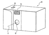
図7、図8は、本発明の結像光学系を用いた電子カメラ(デジタルカメラ)を示すもので、図7は前方より見た斜視図、図8は後方より見た斜視図である。 7 and 8 show an electronic camera (digital camera) using the imaging optical system of the present invention. FIG. 7 is a perspective view seen from the front, and FIG. 8 is a perspective view seen from the rear.
これら図において、10は電子カメラで、撮影用光路11を有する本発明の結像光学系12とシャッター13とフラッシュ14と液晶表示モニター15等を備えている。このカメラ10において、その上部に配置されたシャッター13が押されると、それに連動して本発明の結像光学系12を通して撮影が行なわれる。つまり、この結像光学系12により赤外線カットフィルターを介して図示していないCCD等の撮像素子チップ上に物体像が形成される。
In these drawings,
この撮像素子チップ上に形成された像は、液晶表示モニター上に表示される。 An image formed on the image sensor chip is displayed on a liquid crystal display monitor.
また、図9、図10は、本発明の結像光学系を内蔵した携帯電話を示すもので、図9は正面図、図10は背面図である。 9 and 10 show a mobile phone incorporating the imaging optical system of the present invention. FIG. 9 is a front view and FIG. 10 is a rear view.
これら、図9、図10に示すように、携帯電話20は、操作者の声を入力するマイク部21と、通話相手の声を出力するスピーカー部22と、操作者が情報を入力する操作部23と、操作者自身や通話相手等の撮影像と、電話番号等の情報を表示する例えば液晶表示素子の表示部24と、本発明の結像光学系を含む撮像装置部25と、通話電波の送信と受信を行なうアンテナ26と、背面表示部27と、バッテリ28等を備えている。
As shown in FIGS. 9 and 10, the
本発明の結像光学系は、以上詳細に述べた通りの構成であり、したがって、特許請求の範囲に記載する構成の光学系のほか、次の各項に記載するものも、本発明の目的を達成し得る。 The imaging optical system of the present invention has a configuration as described in detail above. Therefore, in addition to the optical system having the configuration described in the claims, what is described in the following items is also the object of the present invention. Can be achieved.
(1) 特許請求の範囲の請求項1、2又は3に記載する光学系で、次の条件(3)を満足することを特徴とする結像光学系。
(3) 1.0<f23/f<4.0
ただし、f23は第2レンズと第3レンズの合成焦点距離、fは全系の焦点距離である。
(1) An imaging optical system according to
(3) 1.0 <f23 / f <4.0
Here, f23 is the combined focal length of the second lens and the third lens, and f is the focal length of the entire system.
(2) 特許請求の範囲の請求項1、2又は3に記載する光学系で、次の条件(3−1)を満足することを特徴とする結像光学系。
(3−1) 1.3<f23/f<3.0
ただし、f23は第2レンズと第3レンズの合成焦点距離、fは全系の焦点距離である。
(2) An imaging optical system according to
(3-1) 1.3 <f23 / f <3.0
Here, f23 is the combined focal length of the second lens and the third lens, and f is the focal length of the entire system.
(3) 特許請求の範囲の請求項1、2又は3に記載する光学系で、次の条件(3−2)を満足することを特徴とする結像光学系。
(3−2) 1.7<f23/f<2.3
ただし、f23は第2レンズと第3レンズの合成焦点距離、fは全系の焦点距離である。
(3) An imaging optical system according to
(3-2) 1.7 <f23 / f <2.3
Here, f23 is the combined focal length of the second lens and the third lens, and f is the focal length of the entire system.
(4) 特許請求の範囲の請求項1、2又は3あるいは前記の(1)、(2)又は(3)の項に記載する光学系で、下記の条件(4)を満足することを特徴とする結像光学系。
(4) −10.0<f1/f23<3.0
ただし、f1は第1正レンズの焦点距離、f23は第2負レンズと第3正レンズの合成焦点距離である。
(4) The optical system described in
(4) -10.0 <f1 / f23 <3.0
Here, f1 is the focal length of the first positive lens, and f23 is the combined focal length of the second negative lens and the third positive lens.
(5) 特許請求の範囲の請求項1、2又は3あるいは前記の(1)、(2)又は(3)の項に記載する光学系で、下記の条件(4−1)を満足することを特徴とする結像光学系。
(4−1) −1.0<f1/f23<1.0
ただし、f1は第1正レンズの焦点距離、f23は第2負レンズと第3正レンズの合成焦点距離である。
(5) The following condition (4-1) is satisfied in the optical system described in
(4-1) -1.0 <f1 / f23 <1.0
Here, f1 is the focal length of the first positive lens, and f23 is the combined focal length of the second negative lens and the third positive lens.
(6) 特許請求の範囲の請求項1、2又は3あるいは前記の(1)、(2)又は(3)の項に記載する光学系で、下記の条件(4−2)を満足することを特徴とする結像光学系。
(4−2) 0.4<f1/f23<0.7
ただし、f1は第1正レンズの焦点距離、f23は第2負レンズと第3正レンズの合成焦点距離である。
(6) The following condition (4-2) is satisfied in the optical system described in
(4-2) 0.4 <f1 / f23 <0.7
Here, f1 is the focal length of the first positive lens, and f23 is the combined focal length of the second negative lens and the third positive lens.
(7) 特許請求の範囲の請求項1、2又は3あるいは前記の(1)、(2)、(3)、(4)、(5)又は(6)の項に記載する光学系で、下記の条件(5)を満足することを特徴とする結像光学系。
(5) 0.1<−(ν2−ν1)/(ν3−ν2)<8.0
ただし、ν1、ν2、ν3は、夫々第1レンズ、第2レンズ、第3レンズのアッベ数である。
(7) The optical system according to
(5) 0.1 < − (ν2−ν1) / (ν3−ν2) <8.0
Here, ν1, ν2, and ν3 are Abbe numbers of the first lens, the second lens, and the third lens, respectively.
(8) 特許請求の範囲の請求項1、2又は3あるいは前記の(1)、(2)、(3)、(4)、(5)又は(6)の項に記載する光学系で、下記の条件(5−1)を満足することを特徴とする結像光学系。
(5−1) 0.3<−(ν2−ν1)/(ν3−ν2)<3.0
ただし、ν1、ν2、ν3は、夫々第1レンズ、第2レンズ、第3レンズのアッベ数である。
(8) In the optical system according to
(5-1) 0.3 < − (ν2-ν1) / (ν3-ν2) <3.0
Here, ν1, ν2, and ν3 are Abbe numbers of the first lens, the second lens, and the third lens, respectively.
(9) 特許請求の範囲の請求項1、2又は3あるいは前記の(1)、(2)、(3)、(4)、(5)又は(6)の項に記載する光学系で、下記の条件(5−2)を満足することを特徴とする結像光学系。
(5−2) 0.5<−(ν2−ν1)/(ν3−ν2)<1.5
ただし、ν1、ν2、ν3は、夫々第1レンズ、第2レンズ、第3レンズのアッベ数である。
(9) The optical system according to
(5-2) 0.5 < − (ν2-ν1) / (ν3-ν2) <1.5
Here, ν1, ν2, and ν3 are Abbe numbers of the first lens, the second lens, and the third lens, respectively.
(10) 特許請求の範囲の請求項1、2又は3あるいは前記の(1)、(2)、(3)、(4)、(5)、(6)、(7)、(8)又は(9)の項に記載する光学系で、下記の条件(6)を満足することを特徴とする結像光学系。
(6) 10°<α<40°
ただし、αは主光線の像面への最大入射角度である。
(10)
(6) 10 ° <α <40 °
Where α is the maximum incident angle of the chief ray on the image plane.
(11) 特許請求の範囲の請求項1、2又は3あるいは前記の(1)、(2)、(3)、(4)、(5)、(6)、(7)、(8)又は(9)の項に記載する光学系で、下記の条件(6−1)を満足することを特徴とする結像光学系。
(6−1) 12°<α<35°
ただし、αは主光線の像面への最大入射角度である。
(11)
(6-1) 12 ° <α <35 °
Where α is the maximum incident angle of the chief ray on the image plane.
(12) 特許請求の範囲の請求項1、2又は3あるいは前記の(1)、(2)、(3)、(4)、(5)、(6)、(7)、(8)又は(9)の項に記載する光学系で、下記の条件(6−2)を満足することを特徴とする結像光学系。
(6−2) 15°<α<25°
ただし、αは主光線の像面への最大入射角度である。
(12)
(6-2) 15 ° <α <25 °
Where α is the maximum incident angle of the chief ray on the image plane.
(13) 特許請求の範囲の請求項1、2又は3あるいは前記の(1)、(2)、(3)、(4)、(5)、(6)、(7)、(8)、(9)、(10)、(11)又は(12)の項に記載する光学系で、下記の条件(7)を満足することを特徴とする結像光学系。
(7) 0.50[μm]<Fno/P[μm]<2.00[μm]
ただし、Fnoは結像光学系の開放Fナンバー、Pは撮像素子の画素間隔である。
(13)
(7) 0.50 [μm] <Fno / P [μm] <2.00 [μm]
Here, Fno is the open F number of the imaging optical system, and P is the pixel interval of the image sensor.
(14) 特許請求の範囲の請求項1、2又は3あるいは前記の(1)、(2)、(3)、(4)、(5)、(6)、(7)、(8)、(9)、(10)、(11)又は(12)の項に記載する光学系で、下記の条件(7−1)を満足することを特徴とする結像光学系。
(7−1) 0.60[μm]<Fno/P[μm]<1.17[μm]
ただし、Fnoは結像光学系の開放Fナンバー、Pは撮像素子の画素間隔である。
(14)
(7-1) 0.60 [μm] <Fno / P [μm] <1.17 [μm]
Here, Fno is the open F number of the imaging optical system, and P is the pixel interval of the image sensor.
(15) 特許請求の範囲の請求項1、2又は3あるいは前記の(1)、(2)、(3)、(4)、(5)、(6)、(7)、(8)、(9)、(10)、(11)又は(12)の項に記載する光学系で、下記の条件(7−2)を満足することを特徴とする結像光学系。
(7−2) 0.65[μm]<Fno/P[μm]<1.10[μm]
ただし、Fnoは結像光学系の開放Fナンバー、Pは撮像素子の画素間隔である。
(15)
(7-2) 0.65 [μm] <Fno / P [μm] <1.10 [μm]
Here, Fno is the open F number of the imaging optical system, and P is the pixel interval of the image sensor.
(16) 特許請求の範囲の請求項1、2又は3あるいは前記の(1)、(2)、(3)、(4)、(5)、(6)、(7)、(8)、(9)、(10)、(11)又は(12)の項に記載する光学系で、光学系を構成するレンズ中にプラスチックレンズを含み、下記の条件(8)を満足することを特徴とする結像光学系。
(8) 0.02<ML/TL<0.33
ただし、MLはプラスチックレンズにおける最小軸上肉厚、TLは結像光学系の全長である。
(16)
(8) 0.02 <ML / TL <0.33
Where ML is the minimum axial thickness of the plastic lens, and TL is the total length of the imaging optical system.
(17) 特許請求の範囲の請求項1、2又は3あるいは前記の(1)、(2)、(3)、(4)、(5)、(6)、(7)、(8)、(9)、(10)、(11)又は(12)の項に記載する光学系で、光学系を構成するレンズ中にプラスチックレンズを含み、下記の条件(8−1)を満足することを特徴とする結像光学系。
(8−1) 0.04<ML/TL<0.23
ただし、MLはプラスチックレンズにおける最小軸上肉厚、TLは結像光学系の全長である。
(17)
(8-1) 0.04 <ML / TL <0.23
Where ML is the minimum axial thickness of the plastic lens, and TL is the total length of the imaging optical system.
(18) 特許請求の範囲の請求項1、2又は3あるいは前記の(1)、(2)、(3)、(4)、(5)、(6)、(7)、(8)、(9)、(10)、(11)又は(12)の項に記載する光学系で、光学系を構成するレンズ中にプラスチックレンズを含み、下記の条件(8−2)を満足することを特徴とする結像光学系。
(8−2) 0.06<ML/TL<0.17
ただし、MLはプラスチックレンズにおける最小軸上肉厚、TLは結像光学系の全長である。
(18)
(8-2) 0.06 <ML / TL <0.17
Where ML is the minimum axial thickness of the plastic lens, and TL is the total length of the imaging optical system.
(19) 特許請求の範囲の請求項1、2又は3あるいは前記の(1)、(2)、(3)、(4)、(5)、(6)、(7)、(8)、(9)、(10)、(11)、(12)、(13)、(14)、(15)、(16)、(17)又は(18)の項に記載する光学系を備えた光学装置。
(19)
Claims (7)
(3−2) 1.7<f23/f<4.0
ただし、f23は第2レンズと第3レンズの合成焦点距離、fは全系の焦点距離である。 In order from the object side, the third lens includes a first positive meniscus lens having a convex surface directed toward the object side, an aperture stop, a second negative meniscus lens having a convex surface directed toward the image side, and a third positive lens. The object-side surface is an aspheric surface whose curvature decreases toward the periphery, and the image-side surface thereof is an aspheric surface whose curvature increases toward the periphery, and the following condition ( 3-2 ) is satisfied : An imaging optical system characterized by being satisfied.
( 3-2 ) 1. 7 <f23 / f <4.0
Here, f23 is the combined focal length of the second lens and the third lens, and f is the focal length of the entire system.
(1) −100<(r1r2/f1)/(r2f2/f2)<−1
(3) 1.0<f23/f<4.0
ただし、r1rは第1正レンズの像側の面の曲率半径、r2fは第2負レンズの物体側の面の曲率半径、f1は第1正レンズの焦点距離、f2は第2負レンズの焦点距離、f23は第2レンズと第3レンズの合成焦点距離、fは全系の焦点距離である。 In order from the object side, the third lens includes a first positive meniscus lens having a convex surface directed toward the object side, an aperture stop, a second negative meniscus lens having a convex surface directed toward the image side, and a third positive lens. The object-side surface is an aspheric surface whose curvature decreases toward the periphery, and the image-side surface is an aspheric surface whose curvature increases toward the periphery, and the following conditions (1) , (3 ) imaging optical system, characterized by satisfying the.
(1) −100 <(r1r 2 / f1) / (r2f 2 / f2) <− 1
(3) 1.0 <f23 / f <4.0
Where r1r is the radius of curvature of the image side surface of the first positive lens, r2f is the radius of curvature of the object side surface of the second negative lens, f1 is the focal length of the first positive lens, and f2 is the focal point of the second negative lens. The distance , f23 is the combined focal length of the second lens and the third lens, and f is the focal length of the entire system .
(2) 0.1<f1/f<3.0
ただし、f1は第1正レンズの焦点距離、fは全系の焦点距離である。 The imaging optical system according to claim 1 or 2, wherein the following condition (2) is satisfied.
(2) 0.1 <f1 / f <3.0
Here, f1 is the focal length of the first positive lens, and f is the focal length of the entire system.
(4) 0.48≦f1/f23<3.0
ただし、f1は第1正レンズの焦点距離、f23は第2負レンズと第3正レンズの合成焦点距離である。 The imaging optical system according to claim 1, 2 or 3, wherein the following condition (4) is satisfied.
(4) 0.48 ≦ f1 / f23 <3.0
Here, f1 is the focal length of the first positive lens, and f23 is the combined focal length of the second negative lens and the third positive lens.
(3) 1.0<f23/f<4.0
(5) 0.1<−(ν2−ν1)/(ν3−ν2)<8.0
ただし、f23は第2レンズと第3レンズの合成焦点距離、fは全系の焦点距離、ν1、ν2、ν3は、夫々第1レンズ、第2レンズ、第3レンズのアッベ数である。 In order from the object side, the third lens includes a first positive meniscus lens having a convex surface directed toward the object side, an aperture stop, a second negative meniscus lens having a convex surface directed toward the image side, and a third positive lens. The object-side surface is an aspheric surface whose curvature decreases toward the periphery, and the image-side surface thereof is an aspheric surface whose curvature increases toward the periphery, and the following conditions (3), (5 ) An imaging optical system characterized by satisfying
(3) 1.0 <f23 / f <4.0
(5) 0.1 <-(ν2-ν1) / (ν3-ν2) <8.0
Here, f23 is a combined focal length of the second lens and the third lens, f is a focal length of the entire system, and ν1, ν2, and ν3 are Abbe numbers of the first lens, the second lens, and the third lens, respectively.
(7) 0.50[μm]<Fno/P[μm]<2.00[μm]
ただし、Fnoは結像光学系の開放Fナンバー、Pは撮像素子の画素間隔である。 6. An imaging optical system for forming an object image on an image sensor disposed on an imaging surface, wherein the following condition (7) is satisfied: Imaging optical system.
(7) 0.50 [μm] <Fno / P [μm] <2.00 [μm]
Here, Fno is the open F number of the imaging optical system, and P is the pixel interval of the image sensor.
Priority Applications (1)
| Application Number | Priority Date | Filing Date | Title |
|---|---|---|---|
| JP2004065471A JP4616566B2 (en) | 2003-03-12 | 2004-03-09 | Imaging optics |
Applications Claiming Priority (2)
| Application Number | Priority Date | Filing Date | Title |
|---|---|---|---|
| JP2003066815 | 2003-03-12 | ||
| JP2004065471A JP4616566B2 (en) | 2003-03-12 | 2004-03-09 | Imaging optics |
Publications (3)
| Publication Number | Publication Date |
|---|---|
| JP2004295112A JP2004295112A (en) | 2004-10-21 |
| JP2004295112A5 JP2004295112A5 (en) | 2007-04-12 |
| JP4616566B2 true JP4616566B2 (en) | 2011-01-19 |
Family
ID=33421592
Family Applications (1)
| Application Number | Title | Priority Date | Filing Date |
|---|---|---|---|
| JP2004065471A Expired - Fee Related JP4616566B2 (en) | 2003-03-12 | 2004-03-09 | Imaging optics |
Country Status (1)
| Country | Link |
|---|---|
| JP (1) | JP4616566B2 (en) |
Families Citing this family (9)
| Publication number | Priority date | Publication date | Assignee | Title |
|---|---|---|---|---|
| JP2005352317A (en) * | 2004-06-11 | 2005-12-22 | Sony Corp | Imaging lens and imaging unit |
| JP2006178328A (en) | 2004-12-24 | 2006-07-06 | Sony Corp | Imaging lens and imaging apparatus |
| JP4804858B2 (en) * | 2005-09-29 | 2011-11-02 | 富士フイルム株式会社 | Single focus lens |
| JP2008139853A (en) * | 2006-11-08 | 2008-06-19 | Fujinon Corp | Imaging lens having three-lens configuration, camera module, and portable terminal equipment |
| JP2008225332A (en) * | 2007-03-15 | 2008-09-25 | Sony Corp | Imaging lens |
| JP2009053411A (en) * | 2007-08-27 | 2009-03-12 | Hoya Corp | Image reading lens system |
| JP4743225B2 (en) * | 2008-05-07 | 2011-08-10 | ソニー株式会社 | Imaging lens and imaging apparatus |
| KR101804332B1 (en) * | 2010-12-24 | 2018-01-10 | 엘지이노텍 주식회사 | Camera lens module |
| CN114420020A (en) * | 2021-12-15 | 2022-04-29 | 惠州星聚宇智能科技有限公司 | Optical projection system, projection module and welcome lamp |
Citations (6)
| Publication number | Priority date | Publication date | Assignee | Title |
|---|---|---|---|---|
| JPH01307712A (en) * | 1988-06-06 | 1989-12-12 | Konica Corp | Photographic lens |
| JPH04338907A (en) * | 1991-02-19 | 1992-11-26 | Ricoh Opt Ind Co Ltd | Lens for document read |
| JPH1152231A (en) * | 1997-07-31 | 1999-02-26 | Asahi Optical Co Ltd | Read-out lens |
| JP2001051191A (en) * | 1999-08-10 | 2001-02-23 | Sumitomo Electric Ind Ltd | ftheta LENS |
| JP2003185919A (en) * | 2001-12-17 | 2003-07-03 | Nikon Corp | Infrared optical system and infrared optical device having the same |
| JP2007183687A (en) * | 2002-10-25 | 2007-07-19 | Nagano Kogaku Kenkyusho:Kk | Photographic lens for digital camera |
-
2004
- 2004-03-09 JP JP2004065471A patent/JP4616566B2/en not_active Expired - Fee Related
Patent Citations (6)
| Publication number | Priority date | Publication date | Assignee | Title |
|---|---|---|---|---|
| JPH01307712A (en) * | 1988-06-06 | 1989-12-12 | Konica Corp | Photographic lens |
| JPH04338907A (en) * | 1991-02-19 | 1992-11-26 | Ricoh Opt Ind Co Ltd | Lens for document read |
| JPH1152231A (en) * | 1997-07-31 | 1999-02-26 | Asahi Optical Co Ltd | Read-out lens |
| JP2001051191A (en) * | 1999-08-10 | 2001-02-23 | Sumitomo Electric Ind Ltd | ftheta LENS |
| JP2003185919A (en) * | 2001-12-17 | 2003-07-03 | Nikon Corp | Infrared optical system and infrared optical device having the same |
| JP2007183687A (en) * | 2002-10-25 | 2007-07-19 | Nagano Kogaku Kenkyusho:Kk | Photographic lens for digital camera |
Also Published As
| Publication number | Publication date |
|---|---|
| JP2004295112A (en) | 2004-10-21 |
Similar Documents
| Publication | Publication Date | Title |
|---|---|---|
| JP4623993B2 (en) | Imaging optical system and electronic apparatus using the same | |
| US6950246B2 (en) | Imaging optical system and apparatus using the same | |
| JP4466713B6 (en) | Imaging lens and imaging device | |
| JP4658511B2 (en) | Imaging optical system, imaging apparatus and electronic apparatus equipped with the same | |
| US7307799B2 (en) | Imaging optical system | |
| US7006305B2 (en) | Image forming optical system and electronic instrument using the same | |
| US20120224091A1 (en) | Image Pickup Optical System and Image Pickup Apparatus Using the Same | |
| JP4510402B2 (en) | Objective lens and optical instrument | |
| JP4658517B2 (en) | Imaging optical system and electronic apparatus using the same | |
| JP4587702B2 (en) | Imaging optical system and electronic apparatus using the same | |
| JP2007155868A (en) | Imaging lens and imaging apparatus | |
| JP5682806B2 (en) | Imaging optical system, camera device, and portable information terminal device | |
| JP2005024889A (en) | Image-formation optical system and imaging apparatus using the same | |
| JP2004341013A (en) | Imaging optical system and imaging device using the same | |
| JP2005004028A (en) | Imaging optical system and imaging apparatus using it | |
| JP2008020513A (en) | Single focus imaging lens and imaging apparatus equipped therewith | |
| JP2005024581A (en) | Image-formation optical system and imaging apparatus using the same | |
| JP4712318B2 (en) | Imaging optical system and electronic apparatus using the same | |
| JP3757223B2 (en) | Variable magnification imaging lens | |
| JP4616566B2 (en) | Imaging optics | |
| JP4503918B2 (en) | Imaging device | |
| JP2005031638A (en) | Image-formation optical system and electronic equipment using the same | |
| JP4632706B2 (en) | Imaging device | |
| JP2005004027A (en) | Imaging optical system and imaging apparatus using it | |
| JP4819413B2 (en) | Zoom lens and imaging apparatus using the same |
Legal Events
| Date | Code | Title | Description |
|---|---|---|---|
| A521 | Written amendment |
Free format text: JAPANESE INTERMEDIATE CODE: A523 Effective date: 20070223 |
|
| A621 | Written request for application examination |
Free format text: JAPANESE INTERMEDIATE CODE: A621 Effective date: 20070223 |
|
| A977 | Report on retrieval |
Free format text: JAPANESE INTERMEDIATE CODE: A971007 Effective date: 20100422 |
|
| A131 | Notification of reasons for refusal |
Free format text: JAPANESE INTERMEDIATE CODE: A131 Effective date: 20100511 |
|
| A521 | Written amendment |
Free format text: JAPANESE INTERMEDIATE CODE: A523 Effective date: 20100705 |
|
| A131 | Notification of reasons for refusal |
Free format text: JAPANESE INTERMEDIATE CODE: A131 Effective date: 20100727 |
|
| A521 | Written amendment |
Free format text: JAPANESE INTERMEDIATE CODE: A523 Effective date: 20100909 |
|
| TRDD | Decision of grant or rejection written | ||
| A01 | Written decision to grant a patent or to grant a registration (utility model) |
Free format text: JAPANESE INTERMEDIATE CODE: A01 Effective date: 20101012 |
|
| A01 | Written decision to grant a patent or to grant a registration (utility model) |
Free format text: JAPANESE INTERMEDIATE CODE: A01 |
|
| A61 | First payment of annual fees (during grant procedure) |
Free format text: JAPANESE INTERMEDIATE CODE: A61 Effective date: 20101022 |
|
| R151 | Written notification of patent or utility model registration |
Ref document number: 4616566 Country of ref document: JP Free format text: JAPANESE INTERMEDIATE CODE: R151 |
|
| FPAY | Renewal fee payment (event date is renewal date of database) |
Free format text: PAYMENT UNTIL: 20131029 Year of fee payment: 3 |
|
| S531 | Written request for registration of change of domicile |
Free format text: JAPANESE INTERMEDIATE CODE: R313531 |
|
| R350 | Written notification of registration of transfer |
Free format text: JAPANESE INTERMEDIATE CODE: R350 |
|
| R250 | Receipt of annual fees |
Free format text: JAPANESE INTERMEDIATE CODE: R250 |
|
| R250 | Receipt of annual fees |
Free format text: JAPANESE INTERMEDIATE CODE: R250 |
|
| LAPS | Cancellation because of no payment of annual fees |