JP4590054B2 - Shield case mounting structure - Google Patents
Shield case mounting structure Download PDFInfo
- Publication number
- JP4590054B2 JP4590054B2 JP2000009012A JP2000009012A JP4590054B2 JP 4590054 B2 JP4590054 B2 JP 4590054B2 JP 2000009012 A JP2000009012 A JP 2000009012A JP 2000009012 A JP2000009012 A JP 2000009012A JP 4590054 B2 JP4590054 B2 JP 4590054B2
- Authority
- JP
- Japan
- Prior art keywords
- shield case
- solder
- mounting structure
- shape
- wiring board
- Prior art date
- Legal status (The legal status is an assumption and is not a legal conclusion. Google has not performed a legal analysis and makes no representation as to the accuracy of the status listed.)
- Expired - Fee Related
Links
Images


Description
【0001】
【発明の属する技術分野】
本発明は、シールドケースの実装構造に係り、特に、プリント配線基板上に直接取り付けるシールドケースの接続個所の形状に関するものである。
【0002】
【従来の技術】
従来、このような分野の技術としては、以下に示すようなものがあった。
【0003】
図6はかかる従来のシールドケースの実装構造を示す斜視図である。
【0004】
図6に示すように、プリント配線基板1上のグラウンド(GND)パターン2上にシールドケース3を半田4を使用して実装する。すなわち、シールドケース3の側面3aの任意の位置とプリント配線基板1上のGNDパターン2を半田4で接続するようにしている。
【0005】
【発明が解決しようとする課題】
上記した従来のシールドケースの半田による実装においては、図7に示すように、シールドケース3の側面3aが平面である。そのため、シールドケース3をプリント配線基板1に実装するときには、プリント配線基板1〔グラウンド(GND)パターン2〕とシールドケース3の側面3aの両方に半田4を接着する必要がある。
【0006】
この時、プリント配線基板1とシールドケース3の熱抵抗が小さいために、半田ごて5の熱が分散して半田4の温度が低くなりやすく、シールドケース3とプリント配線基板1との接続には大熱容量の半田ごて5が必要になる。
【0007】
しかしながら、大熱容量の半田ごて5を使用すると、この熱がプリント配線基板1のGNDパターン2の周辺にも伝わり、すでに半田によって実装されている電子部品や抵抗・コンデンサ等のチップ部品の半田が溶かされて、これらの部品が動いてしまうという問題がある。
【0008】
また、溶けた半田4がシールドケース3の側面3aに広がってしまうので、半田接続のために多量の半田を必要とする。
【0009】
本発明は、上記問題点を除去し、プリント配線基板上に半田によって実装するシールドケースの半田接続を良好に行えるようにすることを目的とする。
【0010】
【課題を解決するための手段】
本発明は、上記目的を達成するために、シールドケースの実装構造において、プリント配線基板上に半田によって実装するシールドケースの側面の半田接続部分に、前記プリント配線基板と前記シールドケースの下面とが接する部分の前記シールドケースの側面の板厚を線幅とした線状の軌跡が直線形状と前記シールドケースの内側へ突出した曲線形状とからなるように窪み形状部を含む形状部を具備する。また、本発明は、上記目的を達成するために、シールドケースの実装構造において、プリント配線基板上に半田によって実装するシールドケースの側面の半田接続部分に、前記プリント配線基板と前記シールドケースの下面とが接する部分の前記シールドケースの側面の板厚を線幅とした線状の軌跡が直線形状と前記シールドケースの外側へ突出した曲線形状とからなるように突起形状部を含む形状部を具備する。
【0011】
【発明の実施の形態】
以下、本発明の実施の形態について図を参照しながら詳細に説明する。
【0012】
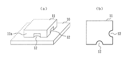
図1は本発明の第1実施例を示すシールドケースの実装構造の要部構成図であり、図1(a)はそのシールドケースの実装構造の要部斜視図、図1(b)はそのシールドケースの実装構造の窪みの形状を示す図(下から見た図)である。
【0013】
この実施例では、シールドケース11の側面11aの半田接続部分を、図1に示すように、窪み形状部12にする。その形状は丸みを有する窪み形状としている。なお、10はプリント配線基板である。
【0014】
この実施例によれば、窪み形状部12に半田(図示なし)の熱が集中しやすくなり、半田の温度が低くなり難い。
【0015】
図2は本発明の第2実施例を示すシールドケースの実装構造の要部構成図であり、図2(a)はそのシールドケースの実装構造の要部斜視図、図2(b)はそのシールドケースの実装構造の突起形状を示す図(下から見た図)である。
【0016】
この実施例では、シールドケース21の側面21aの半田接続部分を、図2に示すように、突起形状部22とする。なお、20はプリント配線基板である。
【0017】
この実施例によれば、突起形状部22に半田(図示なし)の熱が集中しやすくなり、半田の温度が低くなり難い。
【0018】
図3は本発明の第3実施例を示すシールドケースの実装構造の要部斜視図である。
【0019】
この実施例では、シールドケース31の側面31aの半田接続部分を、図3に示すように、ミシン目形状部(小さい窪みが並ぶ)32にする。なお、30はプリント配線基板である。
【0020】
この実施例によれば、ミシン目形状部32があるため、半田はミシン目形状部32の内側の部分に集まりやすくなり、シールドケース31の全体に半田の熱が分散することはない。
【0021】
図4は本発明の第4実施例を示すシールドケースの実装構造の要部斜視図である。
【0022】
この実施例では、シールドケース41の側面41aの半田接続部分を、図4に示すように、半田メッキ形状部42にする。つまり、半田接続部分に半田メッキ加工を施して半田メッキ形状部42を形成している。なお、40はプリント配線基板である。
【0023】
この実施例によれば、その半田メッキ形状部42に半田(図示なし)が接着しやすい。
【0024】
上記したように、本発明によれば、半田ごての熱が半田に集中しやすくなるので、半田の温度は低くなり難くなり、その結果、半田は、窪み形状部12や突起形状部22やミシン目形状部32の内側の部分に集まりやすくなり、シールドケース11,21,31,41と基板10,20,30,40との接続は容易になる。
【0025】
また、半田ごて(図示なし)の熱容量が小さくても半田接続が可能になる。
【0026】
さらに、上記実施例では、半田接続部分を窪み形状部12や突起形状部22やミシン目形状部32の構造とする例と、半田接続部分を、半田メッキ加工の構成の例を別々に示したが、図5に一例を示すように、第1〜第3実施例の半田接続部分の形状部12,22,32の各部分に第4実施例の半田メッキ形状部42を塗布した構成にするようにしてもよい。なお、図5において、51はシールドケース、51aはシールドケースの側面、52は半田接続部分であり、ミシン目形状部32と半田メッキ形状部42とから成っている。
【0027】
なお、本発明は上記実施例に限定されるものではなく、本発明の趣旨に基づいて種々の変形が可能であり、これらを本発明の範囲から排除するものではない。
【0028】
【発明の効果】
以上、詳細に説明したように、本発明によれば、シールドケースの半田接続部分に半田が集中する形状部を形成したので、半田ごての熱は半田に集中しやすくなり、半田の温度は低くなり難くなり、良好な半田による接続を行うことができる。
【図面の簡単な説明】
【図1】本発明の第1実施例を示すシールドケースの実装構造の要部構成図である。
【図2】本発明の第2実施例を示すシールドケースの実装構造の要部構成図である。
【図3】本発明の第3実施例を示すシールドケースの実装構造の要部斜視図である。
【図4】本発明の第4実施例を示すシールドケースの実装構造の要部斜視図である。
【図5】本発明の第5実施例を示すシールドケースの実装構造の要部斜視図である。
【図6】従来のシールドケースの実装構造を示す斜視図である。
【図7】従来のシールドケースの実装工程を示す斜視図である。
【符号の説明】
10,20,30,40,50 プリント配線基板
11,21,31,41,51 シールドケース
11a,21a,31a,41a,51a シールドケースの側面
12 窪み形状部(半田接続部分)
22 突起形状部(半田接続部分)
32 ミシン目形状部
42 半田メッキ形状部
52 半田接続部分(ミシン目形状部+半田メッキ形状部)[0001]
BACKGROUND OF THE INVENTION
The present invention relates to a mounting structure of a shield case, and particularly relates to the shape of a connection portion of a shield case that is directly mounted on a printed wiring board.
[0002]
[Prior art]
Conventionally, there have been the following technologies in such fields.
[0003]
FIG. 6 is a perspective view showing the mounting structure of such a conventional shield case.
[0004]
As shown in FIG. 6, a
[0005]
[Problems to be solved by the invention]
In mounting the above-described conventional shield case with solder, as shown in FIG. 7, the
[0006]
At this time, since the thermal resistance of the printed
[0007]
However, when a large heat capacity soldering
[0008]
Moreover, since the melted solder 4 spreads to the
[0009]
It is an object of the present invention to eliminate the above-mentioned problems and to satisfactorily connect a shield case to be mounted on a printed wiring board with solder.
[0010]
[Means for Solving the Problems]
The present invention, in order to achieve the above object, in the mounting structure of the shield case, the solder connection portion of the side surface of the shield case of mounting by soldering on a printed circuit board, and the printed wiring board and the lower surface of the shield case A shape portion including a hollow shape portion is provided such that a linear locus having a line width as a thickness of a side surface of the shield case at a contacting portion has a linear shape and a curved shape protruding inward of the shield case . In order to achieve the above object, according to the present invention, in the shield case mounting structure, the printed wiring board and the lower surface of the shield case are connected to the solder connection portion of the side surface of the shield case mounted on the printed wiring board by solder. And a shape portion including a protruding shape portion so that a linear trajectory having a line width as a thickness of a side surface of the shield case at a portion in contact with a straight line and a curved shape protruding outward from the shield case To do.
[0011]
DETAILED DESCRIPTION OF THE INVENTION
Hereinafter, embodiments of the present invention will be described in detail with reference to the drawings.
[0012]
FIG. 1 is a configuration diagram of the main part of a shield case mounting structure according to a first embodiment of the present invention, FIG. 1 (a) is a perspective view of the main part of the shield case mounting structure, and FIG. It is a figure (figure seen from the bottom) which shows the shape of the hollow of the mounting structure of a shield case.
[0013]
In this embodiment, the solder connection portion of the
[0014]
According to this embodiment, the heat of solder (not shown) tends to concentrate on the
[0015]
FIG. 2 is a block diagram of the main part of the shield case mounting structure according to the second embodiment of the present invention. FIG. 2 (a) is a perspective view of the main part of the shield case mounting structure, and FIG. It is a figure (view seen from the bottom) which shows the projection shape of the mounting structure of a shield case.
[0016]
In this embodiment, the solder connection portion of the
[0017]
According to this embodiment, the heat of solder (not shown) tends to concentrate on the protrusion-
[0018]
FIG. 3 is a perspective view of an essential part of a shield case mounting structure showing a third embodiment of the present invention.
[0019]
In this embodiment, the solder connection portion of the
[0020]
According to this embodiment, since the
[0021]
FIG. 4 is a perspective view of an essential part of a shield case mounting structure showing a fourth embodiment of the present invention.
[0022]
In this embodiment, the solder connection portion of the
[0023]
According to this embodiment, solder (not shown) is likely to adhere to the solder
[0024]
As described above, according to the present invention, since the heat of the soldering iron is easily concentrated on the solder, the temperature of the solder is difficult to be lowered. It becomes easy to gather at the inner part of the perforated
[0025]
Further, solder connection is possible even if the heat capacity of the soldering iron (not shown) is small.
[0026]
Furthermore, in the said Example, the example which makes a solder connection part the structure of the
[0027]
In addition, this invention is not limited to the said Example, A various deformation | transformation is possible based on the meaning of this invention, and these are not excluded from the scope of the present invention.
[0028]
【The invention's effect】
As described above in detail, according to the present invention, since the shape portion where the solder concentrates is formed at the solder connection portion of the shield case, the heat of the soldering iron is easily concentrated on the solder, and the temperature of the solder is It becomes difficult to lower, and good solder connection can be performed.
[Brief description of the drawings]
FIG. 1 is a configuration diagram of a main part of a shield case mounting structure according to a first embodiment of the present invention;
FIG. 2 is a configuration diagram of the main part of a shield case mounting structure showing a second embodiment of the present invention;
FIG. 3 is a perspective view of an essential part of a shield case mounting structure showing a third embodiment of the present invention;
FIG. 4 is a perspective view of an essential part of a shield case mounting structure showing a fourth embodiment of the present invention;
FIG. 5 is a perspective view of an essential part of a shield case mounting structure showing a fifth embodiment of the present invention;
FIG. 6 is a perspective view showing a conventional shield case mounting structure;
FIG. 7 is a perspective view showing a conventional shield case mounting process.
[Explanation of symbols]
10, 20, 30, 40, 50 Printed
22 Protrusion-shaped part (solder connection part)
32
Claims (3)
ことを特徴とするシールドケースの実装構造。A linear connection with the thickness of the side surface of the shield case at the portion where the printed circuit board and the lower surface of the shield case are in contact with the solder connection portion of the side surface of the shield case mounted by solder on the printed circuit board A shield case mounting structure comprising a shape portion including a hollow shape portion so that a locus is formed of a linear shape and a curved shape protruding inward of the shield case.
ことを特徴とするシールドケースの実装構造。A linear connection with the thickness of the side surface of the shield case at the portion where the printed circuit board and the lower surface of the shield case are in contact with the solder connection portion of the side surface of the shield case mounted by solder on the printed circuit board A shield case mounting structure comprising a shape portion including a protruding shape portion so that a locus is formed of a linear shape and a curved shape protruding outward from the shield case.
ことを特徴とする請求項1又は2に記載のシールドケースの実装構造。3. The shield case mounting structure according to claim 1, wherein the shape portion is subjected to solder plating.
Priority Applications (1)
| Application Number | Priority Date | Filing Date | Title |
|---|---|---|---|
| JP2000009012A JP4590054B2 (en) | 2000-01-18 | 2000-01-18 | Shield case mounting structure |
Applications Claiming Priority (1)
| Application Number | Priority Date | Filing Date | Title |
|---|---|---|---|
| JP2000009012A JP4590054B2 (en) | 2000-01-18 | 2000-01-18 | Shield case mounting structure |
Publications (3)
| Publication Number | Publication Date |
|---|---|
| JP2001203489A JP2001203489A (en) | 2001-07-27 |
| JP2001203489A5 JP2001203489A5 (en) | 2007-03-01 |
| JP4590054B2 true JP4590054B2 (en) | 2010-12-01 |
Family
ID=18537212
Family Applications (1)
| Application Number | Title | Priority Date | Filing Date |
|---|---|---|---|
| JP2000009012A Expired - Fee Related JP4590054B2 (en) | 2000-01-18 | 2000-01-18 | Shield case mounting structure |
Country Status (1)
| Country | Link |
|---|---|
| JP (1) | JP4590054B2 (en) |
Families Citing this family (1)
| Publication number | Priority date | Publication date | Assignee | Title |
|---|---|---|---|---|
| JP6430899B2 (en) * | 2015-06-18 | 2018-11-28 | アルプス電気株式会社 | Circuit module |
Citations (7)
| Publication number | Priority date | Publication date | Assignee | Title |
|---|---|---|---|---|
| JPS59143097U (en) * | 1983-03-11 | 1984-09-25 | シャープ株式会社 | shield case |
| JPH01152693A (en) * | 1988-10-28 | 1989-06-15 | Matsushita Electric Ind Co Ltd | Method of forming radio frequency shielding housing |
| JPH0312356U (en) * | 1989-06-20 | 1991-02-07 | ||
| JPH07212069A (en) * | 1994-01-19 | 1995-08-11 | Hitachi Ltd | Forming method of shield case |
| JPH07263848A (en) * | 1994-03-25 | 1995-10-13 | Fujikura Ltd | Printed wiring board |
| JPH10126030A (en) * | 1996-10-17 | 1998-05-15 | Saitama Nippon Denki Kk | Terminal structure for electronic parts |
| JPH11204954A (en) * | 1998-01-12 | 1999-07-30 | Alps Electric Co Ltd | Electronic apparatus |
Family Cites Families (3)
| Publication number | Priority date | Publication date | Assignee | Title |
|---|---|---|---|---|
| JPS6094834U (en) * | 1983-12-02 | 1985-06-28 | 三洋電機株式会社 | semiconductor equipment |
| JPH09214152A (en) * | 1996-01-30 | 1997-08-15 | Sanyo Electric Co Ltd | Printed board accommodating frame body |
| JP2001036278A (en) * | 1999-07-19 | 2001-02-09 | Sony Corp | Shield case |
-
2000
- 2000-01-18 JP JP2000009012A patent/JP4590054B2/en not_active Expired - Fee Related
Patent Citations (7)
| Publication number | Priority date | Publication date | Assignee | Title |
|---|---|---|---|---|
| JPS59143097U (en) * | 1983-03-11 | 1984-09-25 | シャープ株式会社 | shield case |
| JPH01152693A (en) * | 1988-10-28 | 1989-06-15 | Matsushita Electric Ind Co Ltd | Method of forming radio frequency shielding housing |
| JPH0312356U (en) * | 1989-06-20 | 1991-02-07 | ||
| JPH07212069A (en) * | 1994-01-19 | 1995-08-11 | Hitachi Ltd | Forming method of shield case |
| JPH07263848A (en) * | 1994-03-25 | 1995-10-13 | Fujikura Ltd | Printed wiring board |
| JPH10126030A (en) * | 1996-10-17 | 1998-05-15 | Saitama Nippon Denki Kk | Terminal structure for electronic parts |
| JPH11204954A (en) * | 1998-01-12 | 1999-07-30 | Alps Electric Co Ltd | Electronic apparatus |
Also Published As
| Publication number | Publication date |
|---|---|
| JP2001203489A (en) | 2001-07-27 |
Similar Documents
| Publication | Publication Date | Title |
|---|---|---|
| JP3859422B2 (en) | Soldering method for leaded electronic components | |
| JP4590054B2 (en) | Shield case mounting structure | |
| JPH087655Y2 (en) | Mounting structure for surface mount components | |
| JPH0348490A (en) | Printed wiring board and formation thereof | |
| JP2006208062A (en) | Contact member, contact sheet using contact member, contact substrate, and electronic equipment unit | |
| JPH0955565A (en) | Printed wiring board | |
| JP3928152B2 (en) | Printed wiring board | |
| JP7050718B2 (en) | Positioning jig for soldering | |
| JPH09327980A (en) | Screen printing metal mask of cream solder | |
| JPH0348491A (en) | Printed wiring board | |
| JP3735858B2 (en) | Soldering structure of parts to printed circuit board | |
| JP2503565Y2 (en) | Printed circuit board component mounting structure | |
| JPH11340615A (en) | Printed board | |
| JP3872600B2 (en) | Mounting method of electronic circuit unit | |
| JPS63292689A (en) | Apparatus for circuit wiring of printed substrate | |
| JPH0710969U (en) | Printed board | |
| JPH07273441A (en) | Metal mask for cream solder printing | |
| JPH03229486A (en) | Printed wiring board | |
| JPH02194591A (en) | Printed-circuit board | |
| JP2002111168A (en) | Electronic part with lead wire | |
| JPS6259461B2 (en) | ||
| JPH11330653A (en) | Surface mounting module | |
| JPH04352488A (en) | Organic hybrid integrated circuit | |
| JPH07326851A (en) | Printed circuit | |
| JPH05304348A (en) | Installation structure of flexible printed board |
Legal Events
| Date | Code | Title | Description |
|---|---|---|---|
| A711 | Notification of change in applicant |
Free format text: JAPANESE INTERMEDIATE CODE: A711 Effective date: 20060728 |
|
| RD03 | Notification of appointment of power of attorney |
Free format text: JAPANESE INTERMEDIATE CODE: A7423 Effective date: 20061024 |
|
| A521 | Written amendment |
Free format text: JAPANESE INTERMEDIATE CODE: A523 Effective date: 20070117 |
|
| A621 | Written request for application examination |
Free format text: JAPANESE INTERMEDIATE CODE: A621 Effective date: 20070117 |
|
| A977 | Report on retrieval |
Free format text: JAPANESE INTERMEDIATE CODE: A971007 Effective date: 20090514 |
|
| A131 | Notification of reasons for refusal |
Free format text: JAPANESE INTERMEDIATE CODE: A131 Effective date: 20090518 |
|
| A521 | Written amendment |
Free format text: JAPANESE INTERMEDIATE CODE: A523 Effective date: 20090716 |
|
| A131 | Notification of reasons for refusal |
Free format text: JAPANESE INTERMEDIATE CODE: A131 Effective date: 20090928 |
|
| A521 | Written amendment |
Free format text: JAPANESE INTERMEDIATE CODE: A523 Effective date: 20091127 |
|
| A131 | Notification of reasons for refusal |
Free format text: JAPANESE INTERMEDIATE CODE: A131 Effective date: 20100105 |
|
| A521 | Written amendment |
Free format text: JAPANESE INTERMEDIATE CODE: A523 Effective date: 20100301 |
|
| A02 | Decision of refusal |
Free format text: JAPANESE INTERMEDIATE CODE: A02 Effective date: 20100326 |
|
| A521 | Written amendment |
Free format text: JAPANESE INTERMEDIATE CODE: A523 Effective date: 20100625 |
|
| A911 | Transfer of reconsideration by examiner before appeal (zenchi) |
Free format text: JAPANESE INTERMEDIATE CODE: A911 Effective date: 20100726 |
|
| TRDD | Decision of grant or rejection written | ||
| A01 | Written decision to grant a patent or to grant a registration (utility model) |
Free format text: JAPANESE INTERMEDIATE CODE: A01 Effective date: 20100906 |
|
| A01 | Written decision to grant a patent or to grant a registration (utility model) |
Free format text: JAPANESE INTERMEDIATE CODE: A01 |
|
| A61 | First payment of annual fees (during grant procedure) |
Free format text: JAPANESE INTERMEDIATE CODE: A61 Effective date: 20100913 |
|
| R150 | Certificate of patent or registration of utility model |
Free format text: JAPANESE INTERMEDIATE CODE: R150 |
|
| FPAY | Renewal fee payment (event date is renewal date of database) |
Free format text: PAYMENT UNTIL: 20130917 Year of fee payment: 3 |
|
| LAPS | Cancellation because of no payment of annual fees |