JP4589519B2 - Manufacturing method of semiconductor circuit components - Google Patents
Manufacturing method of semiconductor circuit components Download PDFInfo
- Publication number
- JP4589519B2 JP4589519B2 JP2000342404A JP2000342404A JP4589519B2 JP 4589519 B2 JP4589519 B2 JP 4589519B2 JP 2000342404 A JP2000342404 A JP 2000342404A JP 2000342404 A JP2000342404 A JP 2000342404A JP 4589519 B2 JP4589519 B2 JP 4589519B2
- Authority
- JP
- Japan
- Prior art keywords
- insulating resin
- metal plate
- semiconductor circuit
- manufacturing
- circuit component
- Prior art date
- Legal status (The legal status is an assumption and is not a legal conclusion. Google has not performed a legal analysis and makes no representation as to the accuracy of the status listed.)
- Expired - Fee Related
Links
Images

Classifications
-
- H—ELECTRICITY
- H10—SEMICONDUCTOR DEVICES; ELECTRIC SOLID-STATE DEVICES NOT OTHERWISE PROVIDED FOR
- H10W—GENERIC PACKAGES, INTERCONNECTIONS, CONNECTORS OR OTHER CONSTRUCTIONAL DETAILS OF DEVICES COVERED BY CLASS H10
- H10W74/00—Encapsulations, e.g. protective coatings
- H10W74/10—Encapsulations, e.g. protective coatings characterised by their shape or disposition
- H10W74/15—Encapsulations, e.g. protective coatings characterised by their shape or disposition on active surfaces of flip-chip devices, e.g. underfills
Landscapes
- Production Of Multi-Layered Print Wiring Board (AREA)
Description
【0001】
【発明の属する技術分野】
本発明は、金属板上にビルドアップ形成した絶縁樹脂体に半導体素子を実装し、封止樹脂で樹脂封止した後、金属板をエッチングで除去して形成する半導体回路部品の製造方法に関する。
【0002】
【従来の技術】
近年、半導体素子を実装して形成される半導体回路部品には、半導体素子の高集積化に伴ない半導体素子を搭載する回路基板の配線が高密度化しており、その対応の一例として、ビルドアップ法による多層配線基板が使用されている。このビルドアップ多層配線基板の代表的な製造方法は、先ず、ガラスエポキシ等からなるコア基板にスルーホール用の孔を穿設し、Pd等の触媒を付与し、全面に無電解銅めっきを施し、この上にフォトリソグラフィ法でドライフィルムレジストによる開口部を形成し、無電解銅めっき層に電流を通して開口部に電解銅めっき層を形成する。その後、ドライフィルムを除去し、露出した無電解銅めっき層をエッチングで除去し、無電解銅めっきと電解銅めっきからなる下層側の配線パターン層を形成する。そして、この配線パターン層上にスクリーン印刷やロールコーター等により感光性絶縁樹脂を塗布し、乾燥した後、感光性絶縁樹脂層上にビア形成用のパターンマスクを密着させ、紫外線で露光し、現像することでビアを有する感光性絶縁樹脂層を形成する。次に、この感光性絶縁樹脂層を硬化させて、下層側の絶縁樹脂層とし、このビアを伴う下層側の絶縁樹脂表面をクロム酸、過マンガン酸等の絶縁樹脂粗化液により粗化し、Pd等の触媒を付与した後、全面に無電解銅めっきを行った後、ドライフィルムを貼付し、パターンマスクを密着させ、紫外線で露光し、現像することで配線パターン導体やビア導体となる開口部を形成する。次いで、この開口部に電解銅めっきを形成し、ドライフィルムを剥離後、銅めっき表面をエッチングで、銅めっき層の薄い無電解銅めっき部分を剥離除去し、電解銅めっきで銅めっき層が厚くなった部分の配線パターン導体やビア導体を残すことで上層側の配線パターン層を形成する。以後、同様の工程を順次繰り返して多層化するものである。このようにして形成されたビルドアップ多層配線基板に半導体素子を実装し、封止樹脂で樹脂封止をし、外部端子としての半田ボールを形成して、半導体回路部品としている。
【0003】
【発明が解決しようとする課題】
しかしながら、前述したような従来の半導体回路部品及びその製造方法には、次のような問題がある。
(1)ビルドアップ多層配線基板を形成するには、多数のスルーホールを形成したコア基板を使用するが、このコア基板はビルドアップ多層配線基板の製造コストに占める割合が高い。
(2)一方、市場の要求は低価格の商品にあり、半導体回路部品への更なるコストダウンの要求が高い。しかしながら、現行のコア基板を使用したビルドアップ多層配線基板ではコストダウンの要素が殆どない。
(3)また、近年、半導体素子のクロック周波数の高周波化が急速に進んでおり、この半導体素子を実装する基板にはインダクタンスを低減できる回路設計が求められている。現行のビルドアップ多層配線基板では、コア基板のスルーホール部のインダクタンスがその割合の殆どを占め、コア基板を使用する上ではインダクタンスの低減が期待できない。
(4)さらに、将来、クロック周波数が1GHzを超えると、現行のコア基板を使用してのビルドアップ多層配線基板では対応が困難と予想されている。
本発明は、かかる事情に鑑みてなされたものであって、コア基板を使用しないで、ビルドアップ回路形成がなされた絶縁樹脂体に半導体素子を実装し、安価で高周波特性に優れた半導体回路部品及びその製造方法を提供することを目的とする。
【0004】
【課題を解決するための手段】
前記目的に沿う本発明に係る半導体回路部品は、下面に入出力端子を有し、配線パターン及びビア導体で回路が形成された絶縁樹脂体と半導体素子を接続し、封止樹脂で樹脂封止している半導体回路部品において、金属板上に形成された絶縁樹脂体に、半導体素子が実装され、樹脂封止された後に、金属板をエッチングで除去して形成されている。コア基板を必要としないことから製造コストを低く抑えられ、また、スルーホール部が存在しないので、インダクタンス低減の問題も起こらない。さらに、将来のクロック周波数が1GHzを超えた場合についても対応可能である。
ここで、半導体素子を絶縁樹脂体上面のフリップチップボンディング用のパッドに実装してもよい。これにより、実装面積を小さくすることができ、高密度で小型の半導体回路部品を提供できる。
また、半導体素子を予め電気特性が終了した良品回路の絶縁樹脂体上に実装することができる。これにより、断線やショートのある絶縁樹脂体への実装を避け、高価な半導体素子を無駄にすることがない。
【0005】
前記目的に沿う本発明に係る半導体回路部品の製造方法は、金属板の片面に配線パターン及びビア導体からなる回路を備えた絶縁樹脂体を形成する工程と、回路の入出力端子部を露出するように、金属板にエッチングで孔を穿設し、孔に電気検査用のプローブを挿入し、電気検査する工程と、電気検査で良品とされた絶縁樹脂体に半導体素子を実装し、半導体素子を封止樹脂で封止する工程と、金属板の全てをエッチングで除去する工程とを含み、金属板に絶縁樹脂体を形成する工程の前において、金属板の片面のうち入出力端子部と対向する部分にAuめっきを施す。これにより、コア基板を必要としないので、比較的安価であり、インダクタンス低減の問題が起こらず、クロック周波数が1GHzを超える場合についても対応できる。さらに、半導体素子を実装する前に回路の電気検査を行うことで、良品回路をもつ絶縁樹脂体のみに半導体素子を実装できる。
ここで、複数層からなる絶縁樹脂層で絶縁樹脂体を形成してもよい。これにより、配線密度の高い多端子の半導体回路部品を製造することができる。
さらに、1枚の前記金属板に複数個の前記絶縁樹脂体を形成し、個片化切断することもできる。これにより、効率よく半導体回路部品を製造できる。また、個片化した後に、入出力端子に外部端子として半田ボールを形成することにより、BGA(Ball Grid Array )タイプの半導体回路部品を容易に形成することができる。
【0006】
【発明の実施の形態】
続いて、添付した図面を参照しつつ、本発明を具体化した実施の形態について説明し、本発明の理解に供する。
ここに、図1は本発明の一実施の形態に係る半導体回路部品の部分拡大断面図、図2は本発明の一実施の形態に係る半導体回路部品の製造方法を説明するための部分拡大断面図である。
【0007】
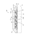
まず、図1を参照して、本発明の一実施の形態に係る半導体回路部品10の構造を説明する。ビルドアップ層を形成するための土台となる金属板11は、例えば、銅、銅合金、42アロイ、SUS304、SUS430等が用いられ、樹脂との密着性を増すために、表面粗化が施されている。この金属板11上に、ソルダーレジスト12が形成されており、その開口部に金属被膜で形成された、入出力端子13が形成されている。ソルダーレジスト12上には、無電解銅めっき及び電解銅めっきにより配線パターン13aが形成されている。さらに、ソルダーレジスト12上には、第1の絶縁樹脂層14が形成され、この第1の絶縁樹脂層14の所定位置には、フォトリソグラフィ法等でビアホール15が形成されている。この第1の絶縁樹脂層14の表面とビアホール15とには、無電解銅めっき及び電解銅めっきにより、第1の配線パターン16とビア導体17が形成(回路の形成)され、入出力端子13と、ソルダーレジスト12上の配線パターン13aを通して、第1の絶縁樹脂層14上の第1の配線パターン16とが、ビア導体17を介して電気的に接続されている。さらに、第1の配線パターン16上に、第2の絶縁樹脂層18が積層され、この第2の絶縁樹脂層18の所定位置にフォトリソグラフィ法等でビアホール15aが形成され、第2の配線パターン19とビア導体17aが形成されている。第1及び第2の絶縁樹脂層14、18によって絶縁樹脂体を形成している。さらに多層にする場合には上記方法を繰り返すことで形成される。
【0008】
最上層の絶縁樹脂層(図1では第2の絶縁樹脂層18)のビアホール15a上に、接続部材20を介して半導体素子21が実装されている。さらに、半導体素子21が封止樹脂22によって樹脂封止されている。封止樹脂22が形成された後、金属板11をエッチングで除去して、下面に入出力端子13を有する半導体回路部品10が形成されている。なお、図1には、絶縁樹脂体は2層分の絶縁樹脂層(ソルダーレジスト層を入れたら3層分)のみが図示されているが、絶縁樹脂層の積層数は1層又は3層以上であってもよい。
【0009】
次に、図1、図2を参照して、本発明の一実施の形態に係る半導体回路部品の製造方法について説明する。
(1)金属板11の片面に回路を備えた絶縁樹脂体を形成する工程
金属板の片面にビルドアップ法により回路を形成するので、金属板は反りやすい。そこで、この金属板の選択として、反りを最小限に抑制するために、絶縁樹脂材料との熱膨張率差が小さく、且つ反りに対してある程度の機械強度を持つ材質が要求される。また、量産に適用できる安価である材質も要求される。その結果、銅、銅合金、42アロイ、SUS304、SUS430等が揚げられるが、好ましい形態としては銅又は銅合金が選択される。板厚みは0.1〜0.5mm程度のものを使用する。ビルドアップに使用する材料は、既存のいずれの材料であっても適用可能である。また、プロセスについても既存のビア形成であるフォトビア方式、レーザービア方式等があり、回路形成方法としては、サブトラクティブ法、セミアディティブ法、フルアディティブ法等があり、特に限定するものではない。
【0010】
ここでは、板厚み0.3mm程度のタフピッチ銅からなる金属板11を使用して、セミアディティブ法によるビルドアップの製造方法で説明する。先ず、金属板11と樹脂との密着性を高めるために、金属板11の表面にジェットスクラブ処理等を施して表面粗化をする。金属板11の裏面は、各種めっきやエッチングの処理から保護するために、耐薬品性に優れたカバーフィルムを形成する。この金属板11の表面に、感光性のソルダーレジスト12を約20μm程度全面印刷し、フォトリソグラフィ法により、パターンマスクを載置し、例えば、600mJ/cm2 の紫外線で露光し、現像処理を行い、さらに、紫外線キュア、熱キュアを行い、硬化させて、入出力端子13になる開口部を形成する。この開口部の金属板11の表面には、金属被膜、例えば、Auめっき、Niめっきを施す。なお、金属被膜として、Auめっき及びNiめっきを施す場合は、後述する金属板11を除去するときにAuめっき面がめっきレジストとなるようにAuめっきを先に行い、Niめっきを後に行う必要がある。Auめっき、Niめっきは電解めっき、無電解めっき何れでもよく、めっき厚はAuめっきがMax0.1μm程度であり、NiめっきがMax5μm程度である。
【0011】
次いで、ソルダーレジスト12の表面に配線パターン13aを形成する。これには、先ず、ソルダーレジスト12と銅めっきとの密着性を高めるために、ソルダーレジスト12の表面をクロム酸、過マンガン酸カリウム等により表面粗化をする。次いで、Pd等の触媒を付与した後、無電解銅めっきを施し、その上に感光性のドライフィルムレジストをラミネートし、パターンマスクを密着させ露光し、現像し、ドライフィルムレジストによる開口部を形成する。その後、無電解銅めっき層を通して電流を流し、開口部に電解銅めっき層を形成する。次に、ドライフィルムレジストを除去し、エッチングすることで、無電解銅めっき層のみの銅厚みの薄い部分をエッチング除去し、無電解銅めっきと電解銅めっきから成る配線パターン13aを形成する。
【0012】
次に、樹脂との密着性を高めるために、銅の配線パターン13aの表面をCZ処理等で表面粗化した後、ソルダーレジスト12上に感光性絶縁樹脂をスクリーン印刷やロールコーター等により塗布し、乾燥した後、パターンマスクを密着させ、紫外線で露光し、現像することでビアホール15を開口させ、次いで、紫外線キュア、熱キュアを行い、硬化させて、第1の絶縁樹脂層14を形成する。この第1の絶縁樹脂層14上に、第1の配線パターン16及びビア導体17からなる回路を形成する方法は、上記ソルダーレジスト12上に、配線パターン13a、及び入出力端子13部を形成した方法と同様の方法を採用する。
更に、上記方法を繰り返して行って、第2の絶縁樹脂層18、ビアホール15a、第2の配線パターン19、ビア導体17aを形成する。
半導体素子が実装される第2の絶縁樹脂層18上の第2の配線パターン19及びビア導体17aの回路を形成した後、ソルダーレジストや金属被膜、例えば、Niめっき、Auめっき等を施す。
上記工程により、金属板11上に、半導体素子実装用の絶縁樹脂体が形成される。
【0013】
(2)電気検査工程
通常、半導体素子実装用パッケージは、半導体素子21を実装する前にパッケージとしての回路の断線、ショートの電気検査を実施する。これは、高価な半導体素子を半導体素子実装用パッケージに実装した後に、半導体素子実装用パッケージの電気的不具合により機能できないことを防止するためである。しかしながら、本発明の実施の形態では、金属板11の上に半導体素子実装用の絶縁樹脂体を形成し、この状態で半導体素子21を実装するので、金属板11によって全ての端子がショートの状態にある。そこで、この電気検査を可能にする方法が、この工程である。
先ず、金属板11の裏面に形成されているカバーフィルムを剥離し、感光性のドライフィルムを貼付し、パターンマスクを載置し、紫外線露光、現像を行って、入出力端子13の部分を露出させるに足る大きさの開口部を形成する。次いで、ドライフィルムをエッチングレジストとして、ドライフィルムの開口部の金属板11を通常のエッチング液、例えば、FeCl3 等のエッチング液を使用してエッチングをし、除去する。電気検査は金属板11の開口された孔23にプローブ24を挿入し、入出力端子13側と半導体素子の接続端子間を検査することができる断線、ショート検査機で検査する。検査結果での良品とされた絶縁樹脂体のみが半導体素子実装用に供される。
なお、多数の絶縁樹脂体を1枚の大型パネルで製作される場合には、この電気検査の結果をパネル上の個々の絶縁樹脂体に反映させる手段、例えば、不良絶縁樹脂体にマーキングを施す等の処置をすることが好ましい。
【0014】
(3)半導体素子実装、樹脂封止工程
電気検査で良品となった絶縁樹脂体上に接続部材20を介して半導体素子21を載置し、赤外線リフロー炉やオーブン等で加熱し、接続する。接続方法はフリップチップボンディング方式が好ましい形態である。接続部材20は通常半田バンプや、ワイヤボンディングを利用したAuボールバンプや、あるいは、Auめっきバンプ等が絶縁樹脂体側のビアホール部及び/又は、半導体素子21の接続パッドに形成される。
半導体素子21が絶縁樹脂体に実装された後、半導体素子21を封止樹脂22で樹脂封止する。その方法は特に限定されるものではなく、通常のポッティング方式やトランスファーモールド方式等で行われる。
【0015】
(4)金属板除去工程
金属板11の全てを通常のエッチング液、例えば、FeCl3 等のエッチング液を使用してエッチングし、除去することで、半導体回路部品10となる。
多数個の絶縁樹脂体を1枚の大型パネルで製作する場合には、ダイシングソー等で個片化切断して個々の半導体回路部品10とする。
【0016】
(5)外部端子形成工程
個片化された半導体回路部品10の入出力端子13に外部端子としての半田ボール25を形成する。この半田ボール25は、フラックスを使用した半田ボール転写方式により、半田ボールを所定の位置に配置させ、赤外線リフロー炉やオーブン等による加熱処理によって形成される。
【0017】
【発明の効果】
請求項1〜3記載の半導体回路部品においては、絶縁樹脂体は金属板上に形成され、半導体素子が実装され、樹脂封止(気密封止)された後に、金属板をエッチングで除去して形成されているので、半導体回路部品にコア基板がつかわれていない。従って、製造コストを低く抑えられることができる。また、コア基板を使用していないのでスルーホールが存在せず、インダクタンス低減の問題は起こらない。さらに、将来のクロック周波数が1GHzを超えても対応可能となる。
特に、請求項2記載の半導体回路部品においては、半導体素子は絶縁樹脂体上面のフリップチップボンディング用のパッドに実装されるので、僅かな実装面積ですみ、高密度で小型の半導体回路部品を提供できる。
請求項3記載の半導体回路部品においては、半導体素子は予め電気特性が終了した良品回路の絶縁樹脂体上に実装されているので、不良の絶縁樹脂体には実装されることがなく、高価な半導体素子を無駄にすることがない。
【0018】
請求項4〜6記載の半導体回路部品の製造方法は、金属板の片面に絶縁樹脂と配線パターン及びビア導体からなる回路を備えた絶縁樹脂体を形成する工程と、回路の入出力端子部を露出するように、金属板にエッチングで孔を穿設し、孔に電気検査用のプローブを挿入し、電気検査する工程と、電気検査で良品の絶縁樹脂体に半導体素子を実装し、半導体素子を封止樹脂で封止する工程と、金属板の全てをエッチングで除去する工程とを含むので、コア基板を必要とせず、比較的安価に製造でき、インダクタンス低減の問題が起こらず、クロック周波数1GHzについても対応でき、さらに、半導体素子を実装する前に回路の電気検査を行うことで、良品回路の絶縁樹脂体のみに半導体素子を実装できる。
特に、請求項5記載の半導体回路部品の製造方法においては、複数層からなる絶縁樹脂層で絶縁樹脂体を形成するので、配線密度の高い多端子の半導体回路部品の製造ができる。
請求項6記載の半導体回路部品の製造方法においては、1枚の金属板に複数個の絶縁樹脂体を形成し、個片化切断するので、効率よく形成できる。
【図面の簡単な説明】
【図1】 本発明の一実施の形態に係る半導体回路部品の部分拡大断面図である。
【図2】 本発明の一実施の形態に係る半導体回路部品の製造方法を説明するための部分拡大断面図である。
【符号の説明】
10:半導体回路部品、11:金属板、12:ソルダーレジスト、13:入出力端子、13a:配線パターン、14:第1の絶縁樹脂層、15:ビアホール、15a:ビアホール、16:第1の配線パターン、17:ビア導体、17a:ビア導体、18:第2の絶縁樹脂層、19:第2の配線パターン、20:接続部材、21:半導体素子、22:封止樹脂、23:孔、24:プローブ、25:半田ボール[0001]
BACKGROUND OF THE INVENTION
The present invention is a semiconductor device mounted on the insulating resin body obtained by buildup on the metal plate, after resin sealing with the sealing resin, a method of manufacturing a semiconductor circuit portion product formed by removing the metal plate by etching .
[0002]
[Prior art]
In recent years, in semiconductor circuit components formed by mounting semiconductor elements, the wiring density of circuit boards on which semiconductor elements are mounted has become higher due to the higher integration of semiconductor elements. A multilayer wiring board by the method is used. A typical manufacturing method for this build-up multilayer wiring board is to first drill a hole for a through hole in a core substrate made of glass epoxy or the like, apply a catalyst such as Pd, and perform electroless copper plating on the entire surface. On this, an opening made of a dry film resist is formed by a photolithography method, and an electrolytic copper plating layer is formed in the opening by passing a current through the electroless copper plating layer. Thereafter, the dry film is removed, the exposed electroless copper plating layer is removed by etching, and a lower wiring pattern layer made of electroless copper plating and electrolytic copper plating is formed. Then, a photosensitive insulating resin is applied onto the wiring pattern layer by screen printing or a roll coater and dried, and then a pattern mask for forming vias is brought into close contact with the photosensitive insulating resin layer, exposed to ultraviolet rays, and developed. As a result, a photosensitive insulating resin layer having vias is formed. Next, the photosensitive insulating resin layer is cured to form a lower insulating resin layer, and the lower insulating resin surface with the vias is roughened with an insulating resin roughening solution such as chromic acid or permanganic acid, After applying a catalyst such as Pd, electroless copper plating is applied to the entire surface, then a dry film is applied, a pattern mask is adhered, exposed to ultraviolet rays, and developed to provide openings for wiring pattern conductors and via conductors. Forming part. Next, electrolytic copper plating is formed in this opening, and after the dry film is peeled off, the copper plating surface is etched and the thin electroless copper plating portion of the copper plating layer is peeled off and the copper plating layer is thickened by electrolytic copper plating. The wiring pattern layer on the upper layer side is formed by leaving the wiring pattern conductor and via conductor in the formed portion. Thereafter, the same process is sequentially repeated to form a multilayer. A semiconductor element is mounted on the build-up multilayer wiring board formed as described above, resin-sealed with a sealing resin, and solder balls as external terminals are formed to form a semiconductor circuit component.
[0003]
[Problems to be solved by the invention]
However, the conventional semiconductor circuit components and the manufacturing method thereof as described above have the following problems.
(1) To form a build-up multilayer wiring board, a core board having a large number of through holes is used, and this core board accounts for a large proportion of the manufacturing cost of the build-up multilayer wiring board.
(2) On the other hand, the market demand is for low-priced products, and there is a high demand for further cost reduction of semiconductor circuit components. However, the build-up multilayer wiring board using the current core board has almost no cost reduction factor.
(3) In recent years, the clock frequency of semiconductor elements has been rapidly increased, and a circuit design capable of reducing inductance is required for a substrate on which the semiconductor elements are mounted. In the current build-up multilayer wiring board, the inductance of the through hole portion of the core board occupies most of the ratio, and reduction of the inductance cannot be expected when the core board is used.
(4) Furthermore, when the clock frequency exceeds 1 GHz in the future, it is expected that it is difficult to cope with the build-up multilayer wiring board using the current core board.
SUMMARY OF THE INVENTION The present invention has been made in view of such circumstances, and is a semiconductor circuit component that is inexpensive and has excellent high-frequency characteristics by mounting a semiconductor element on an insulating resin body on which a build-up circuit is formed without using a core substrate. And it aims at providing the manufacturing method.
[0004]
[Means for Solving the Problems]
The semiconductor circuit component according to the present invention that meets the above-mentioned object has an input / output terminal on the lower surface, connects an insulating resin body in which a circuit is formed with a wiring pattern and a via conductor, and a semiconductor element, and is sealed with a sealing resin. In a semiconductor circuit component, a semiconductor element is mounted on an insulating resin body formed on a metal plate and sealed with resin, and then the metal plate is removed by etching. Since a core substrate is not required, the manufacturing cost can be kept low, and since there is no through-hole portion, there is no problem of inductance reduction. Furthermore, it is possible to cope with a case where the future clock frequency exceeds 1 GHz.
Here, the semiconductor element may be mounted on a pad for flip chip bonding on the upper surface of the insulating resin body. As a result, the mounting area can be reduced, and a high-density and small-sized semiconductor circuit component can be provided.
In addition, the semiconductor element can be mounted on an insulating resin body of a non-defective circuit whose electrical characteristics have been finished in advance. Thus, mounting on an insulating resin body having a disconnection or a short circuit is avoided, and an expensive semiconductor element is not wasted.
[0005]
A method of manufacturing a semiconductor circuit component according to the present invention that meets the above-described object includes a step of forming an insulating resin body having a circuit comprising a wiring pattern and a via conductor on one side of a metal plate, and exposing an input / output terminal portion of the circuit. As described above, a hole is formed by etching in a metal plate, a probe for electrical inspection is inserted into the hole, electrical inspection is performed, and a semiconductor element is mounted on an insulating resin body that has been judged to be non-defective by electrical inspection. a step of sealing with a sealing resin, saw including a step of removing all of the metal plate by etching, before the step of forming the insulating resin material in a metal plate, input-output terminal portions of the one surface of the metal plate Au plating is applied to the part opposite to . Thereby, since the core substrate is not required, it is relatively inexpensive, the problem of inductance reduction does not occur, and the case where the clock frequency exceeds 1 GHz can be dealt with. Furthermore, by conducting an electrical inspection of the circuit before mounting the semiconductor element, the semiconductor element can be mounted only on an insulating resin body having a non-defective circuit.
Here, the insulating resin body may be formed of an insulating resin layer composed of a plurality of layers. Thereby, a multi-terminal semiconductor circuit component having a high wiring density can be manufactured.
Further, a plurality of the insulating resin bodies can be formed on one metal plate and cut into pieces. Thereby, a semiconductor circuit component can be manufactured efficiently. Further, by forming solder balls as external terminals on the input / output terminals after the separation, a BGA (Ball Grid Array) type semiconductor circuit component can be easily formed.
[0006]
DETAILED DESCRIPTION OF THE INVENTION
Next, embodiments of the present invention will be described with reference to the accompanying drawings to provide an understanding of the present invention.
FIG. 1 is a partially enlarged sectional view of a semiconductor circuit component according to an embodiment of the present invention. FIG. 2 is a partially enlarged sectional view for explaining a method for manufacturing a semiconductor circuit component according to an embodiment of the present invention. FIG.
[0007]
First, the structure of a
[0008]
A
[0009]
Next, a method for manufacturing a semiconductor circuit component according to an embodiment of the present invention will be described with reference to FIGS.
(1) Process of forming an insulating resin body having a circuit on one side of the
[0010]
Here, a description will be given of a build-up manufacturing method by a semi-additive method using a
[0011]
Next, a
[0012]
Next, in order to improve the adhesion to the resin, the surface of the
Further, the above method is repeated to form the second insulating
After the circuit of the
Through the above process, an insulating resin body for mounting a semiconductor element is formed on the
[0013]
(2) Electrical inspection process Normally, a semiconductor element mounting package performs an electrical inspection of circuit breakage and short circuit as a package before mounting the
First, the cover film formed on the back surface of the
When a large number of insulating resin bodies are manufactured with a single large panel, means for reflecting the result of this electrical inspection on individual insulating resin bodies on the panel, for example, marking is performed on defective insulating resin bodies. It is preferable to perform such treatment.
[0014]
(3) Mounting of semiconductor element and resin sealing process
After the
[0015]
(4) Metal plate removal step The
When manufacturing a large number of insulating resin bodies with a single large panel, the individual
[0016]
(5) External terminal formation
[0017]
【The invention's effect】
4. The semiconductor circuit component according to claim 1, wherein the insulating resin body is formed on the metal plate, the semiconductor element is mounted, and after the resin sealing (airtight sealing), the metal plate is removed by etching. Since it is formed, the core substrate is not used for the semiconductor circuit component. Therefore, the manufacturing cost can be kept low. Further, since the core substrate is not used, there is no through hole, and there is no problem of inductance reduction. Furthermore, it is possible to cope with future clock frequencies exceeding 1 GHz.
Particularly, in the semiconductor circuit component according to claim 2, since the semiconductor element is mounted on the flip chip bonding pad on the upper surface of the insulating resin body, a small mounting area is required, and a high-density and small-sized semiconductor circuit component is provided. it can.
In the semiconductor circuit component according to claim 3, since the semiconductor element is mounted on the insulating resin body of a non-defective circuit whose electrical characteristics have been finished in advance, it is not mounted on a defective insulating resin body and is expensive. There is no waste of semiconductor elements.
[0018]
A method of manufacturing a semiconductor circuit component according to claim 4, wherein a step of forming an insulating resin body provided with a circuit comprising an insulating resin, a wiring pattern and a via conductor on one side of a metal plate, and an input / output terminal portion of the circuit are provided. A hole is formed by etching in the metal plate so as to be exposed, a probe for electrical inspection is inserted into the hole, and an electrical inspection is performed, and a semiconductor element is mounted on a non-defective insulating resin body by electrical inspection. Including a step of sealing the metal plate with a sealing resin and a step of removing all of the metal plate by etching, so that a core substrate is not required and can be manufactured at a relatively low cost, without causing problems of inductance reduction, and a clock frequency. 1 GHz can also be supported, and furthermore, by conducting an electrical inspection of the circuit before mounting the semiconductor element, the semiconductor element can be mounted only on the insulating resin body of the non-defective circuit.
In particular, in the method of manufacturing a semiconductor circuit component according to claim 5, since the insulating resin body is formed by the insulating resin layer composed of a plurality of layers, a multi-terminal semiconductor circuit component having a high wiring density can be manufactured.
In the method of manufacturing a semiconductor circuit component according to claim 6, since a plurality of insulating resin bodies are formed on a single metal plate and cut into pieces, it can be formed efficiently.
[Brief description of the drawings]
FIG. 1 is a partially enlarged cross-sectional view of a semiconductor circuit component according to an embodiment of the present invention.
FIG. 2 is a partially enlarged cross-sectional view for explaining a method for manufacturing a semiconductor circuit component according to one embodiment of the present invention.
[Explanation of symbols]
10: semiconductor circuit component, 11: metal plate, 12: solder resist, 13: input / output terminal, 13a: wiring pattern, 14: first insulating resin layer, 15: via hole, 15a: via hole, 16: first wiring Pattern: 17: Via conductor, 17a: Via conductor, 18: Second insulating resin layer, 19: Second wiring pattern, 20: Connection member, 21: Semiconductor element, 22: Sealing resin, 23: Hole, 24 : Probe, 25: Solder ball
Claims (4)
前記金属板に前記絶縁樹脂体を形成する工程の前において、前記金属板の前記片面のうち前記入出力端子部と対向する部分にAuめっきを施す半導体回路部品の製造方法。A step of forming an insulating resin body provided with a circuit comprising a wiring pattern and a via conductor on one side of the metal plate, and a hole is formed in the metal plate by etching so as to expose an input / output terminal portion of the circuit; Inserting a probe for electrical inspection into the hole and performing electrical inspection; mounting a semiconductor element on the insulating resin body made good by the electrical inspection; and sealing the semiconductor element with a sealing resin; , look-containing and a step of removing all of the metal plate by etching,
Prior to the step of forming the insulating resin body on the metal plate, a method of manufacturing a semiconductor circuit component in which Au plating is performed on a portion of the one surface of the metal plate facing the input / output terminal portion .
前記Auめっきを施す前に、前記金属板の前記片面に、前記入出力端子部を形成する部分に開口部を有するソルダーレジスト層を形成し、Before applying the Au plating, a solder resist layer having an opening in the portion where the input / output terminal portion is formed is formed on the one surface of the metal plate,
前記絶縁樹脂体を形成する工程において、前記ソルダーレジスト層上に前記絶縁樹脂体を形成する半導体回路部品の製造方法。A method of manufacturing a semiconductor circuit component, wherein in the step of forming the insulating resin body, the insulating resin body is formed on the solder resist layer.
Priority Applications (1)
| Application Number | Priority Date | Filing Date | Title |
|---|---|---|---|
| JP2000342404A JP4589519B2 (en) | 2000-11-09 | 2000-11-09 | Manufacturing method of semiconductor circuit components |
Applications Claiming Priority (1)
| Application Number | Priority Date | Filing Date | Title |
|---|---|---|---|
| JP2000342404A JP4589519B2 (en) | 2000-11-09 | 2000-11-09 | Manufacturing method of semiconductor circuit components |
Publications (2)
| Publication Number | Publication Date |
|---|---|
| JP2002151622A JP2002151622A (en) | 2002-05-24 |
| JP4589519B2 true JP4589519B2 (en) | 2010-12-01 |
Family
ID=18816967
Family Applications (1)
| Application Number | Title | Priority Date | Filing Date |
|---|---|---|---|
| JP2000342404A Expired - Fee Related JP4589519B2 (en) | 2000-11-09 | 2000-11-09 | Manufacturing method of semiconductor circuit components |
Country Status (1)
| Country | Link |
|---|---|
| JP (1) | JP4589519B2 (en) |
Families Citing this family (6)
| Publication number | Priority date | Publication date | Assignee | Title |
|---|---|---|---|---|
| JP2005251780A (en) * | 2004-03-01 | 2005-09-15 | Matsushita Electric Ind Co Ltd | Semiconductor circuit component and manufacturing method thereof |
| CN1791311B (en) * | 2004-12-01 | 2012-02-22 | 新光电气工业株式会社 | Method of manufacturing a circuit substrate and method of manufacturing an electronic parts packaging structure |
| JP5653144B2 (en) * | 2004-12-16 | 2015-01-14 | 新光電気工業株式会社 | Manufacturing method of semiconductor package |
| KR100887475B1 (en) * | 2007-02-26 | 2009-03-10 | 주식회사 네패스 | Semiconductor package and manufacturing method |
| JP5545779B2 (en) * | 2012-11-06 | 2014-07-09 | 新光電気工業株式会社 | WIRING BOARD, MANUFACTURING METHOD THEREOF, AND SEMICONDUCTOR DEVICE |
| JP7007882B2 (en) | 2017-12-08 | 2022-01-25 | 新光電気工業株式会社 | Wiring board and its manufacturing method |
Family Cites Families (4)
| Publication number | Priority date | Publication date | Assignee | Title |
|---|---|---|---|---|
| JPS62156898A (en) * | 1985-12-28 | 1987-07-11 | 株式会社東芝 | Manufacture of through-hole printed wiring board |
| CN1117395C (en) * | 1994-03-18 | 2003-08-06 | 日立化成工业株式会社 | Manufacturing method of semiconductor component and semiconductor component |
| JP3400877B2 (en) * | 1994-12-14 | 2003-04-28 | 三菱電機株式会社 | Semiconductor device and manufacturing method thereof |
| JP4282777B2 (en) * | 1996-10-16 | 2009-06-24 | 株式会社トッパンNecサーキットソリューションズ | Semiconductor device substrate and semiconductor device manufacturing method |
-
2000
- 2000-11-09 JP JP2000342404A patent/JP4589519B2/en not_active Expired - Fee Related
Also Published As
| Publication number | Publication date |
|---|---|
| JP2002151622A (en) | 2002-05-24 |
Similar Documents
| Publication | Publication Date | Title |
|---|---|---|
| US7506437B2 (en) | Printed circuit board having chip package mounted thereon and method of fabricating same | |
| JP4057589B2 (en) | Manufacturing method of electronic component mounting board | |
| US7256495B2 (en) | Package substrate manufactured using electrolytic leadless plating process, and method for manufacturing the same | |
| JP3670917B2 (en) | Semiconductor device and manufacturing method thereof | |
| JP3895303B2 (en) | Method for manufacturing package substrate without using plated lead | |
| JP3429734B2 (en) | Wiring board, multilayer wiring board, circuit component package, and method of manufacturing wiring board | |
| KR100896810B1 (en) | Printed Circuit Board and Manufacturing Method | |
| JPH11233678A (en) | Manufacturing method of IC package | |
| JP4589519B2 (en) | Manufacturing method of semiconductor circuit components | |
| KR100547349B1 (en) | Semiconductor Package Substrate and Manufacturing Method Thereof | |
| WO2007066563A1 (en) | Printed wiring board with component-mounting pins and electronic equipment using the same | |
| JP4090151B2 (en) | Package substrate | |
| JP3037603B2 (en) | Printed circuit board for semiconductor package | |
| JP2500404B2 (en) | Circuit board mounting structure | |
| KR100296001B1 (en) | Multi-layer hybrid integrated circuit manufacturing method | |
| US6968613B2 (en) | Fabrication method of circuit board | |
| JP2002064273A (en) | Multilayer printed circuit board | |
| JP2001274203A (en) | 2-metal substrate and BGA structure | |
| JP4696368B2 (en) | Semiconductor package substrate and manufacturing method thereof, and semiconductor package and manufacturing method thereof | |
| JP2001274204A (en) | 2-metal substrate and BGA structure | |
| JP4137295B2 (en) | CSP tape carrier manufacturing method | |
| CN115692207A (en) | Packaging substrate and manufacturing method thereof | |
| JPH11224919A (en) | Substrate for semiconductor device | |
| JP2001267708A (en) | Printed wiring board and its manufacturing method | |
| JP2001244303A (en) | Insulating base material with adhesive used for semiconductor mounting substrate, method of manufacturing the same, semiconductor mounting substrate using the same, and method of manufacturing the same |
Legal Events
| Date | Code | Title | Description |
|---|---|---|---|
| A711 | Notification of change in applicant |
Free format text: JAPANESE INTERMEDIATE CODE: A711 Effective date: 20070314 |
|
| RD01 | Notification of change of attorney |
Free format text: JAPANESE INTERMEDIATE CODE: A7421 Effective date: 20070314 |
|
| A521 | Request for written amendment filed |
Free format text: JAPANESE INTERMEDIATE CODE: A821 Effective date: 20070314 |
|
| A621 | Written request for application examination |
Free format text: JAPANESE INTERMEDIATE CODE: A621 Effective date: 20071015 |
|
| A977 | Report on retrieval |
Free format text: JAPANESE INTERMEDIATE CODE: A971007 Effective date: 20080131 |
|
| A131 | Notification of reasons for refusal |
Free format text: JAPANESE INTERMEDIATE CODE: A131 Effective date: 20100615 |
|
| A521 | Request for written amendment filed |
Free format text: JAPANESE INTERMEDIATE CODE: A523 Effective date: 20100816 |
|
| TRDD | Decision of grant or rejection written | ||
| A01 | Written decision to grant a patent or to grant a registration (utility model) |
Free format text: JAPANESE INTERMEDIATE CODE: A01 Effective date: 20100907 |
|
| A01 | Written decision to grant a patent or to grant a registration (utility model) |
Free format text: JAPANESE INTERMEDIATE CODE: A01 |
|
| A61 | First payment of annual fees (during grant procedure) |
Free format text: JAPANESE INTERMEDIATE CODE: A61 Effective date: 20100910 |
|
| R150 | Certificate of patent or registration of utility model |
Free format text: JAPANESE INTERMEDIATE CODE: R150 |
|
| FPAY | Renewal fee payment (event date is renewal date of database) |
Free format text: PAYMENT UNTIL: 20130917 Year of fee payment: 3 |
|
| A521 | Request for written amendment filed |
Free format text: JAPANESE INTERMEDIATE CODE: A523 Effective date: 20100816 |
|
| LAPS | Cancellation because of no payment of annual fees |