JP4586146B2 - Electrodynamic micromirror device and method for manufacturing the same - Google Patents
Electrodynamic micromirror device and method for manufacturing the same Download PDFInfo
- Publication number
- JP4586146B2 JP4586146B2 JP2006538296A JP2006538296A JP4586146B2 JP 4586146 B2 JP4586146 B2 JP 4586146B2 JP 2006538296 A JP2006538296 A JP 2006538296A JP 2006538296 A JP2006538296 A JP 2006538296A JP 4586146 B2 JP4586146 B2 JP 4586146B2
- Authority
- JP
- Japan
- Prior art keywords
- micromirror
- layer
- micromirrors
- forming
- mirror
- Prior art date
- Legal status (The legal status is an assumption and is not a legal conclusion. Google has not performed a legal analysis and makes no representation as to the accuracy of the status listed.)
- Expired - Fee Related
Links
Images


Classifications
-
- G—PHYSICS
- G02—OPTICS
- G02B—OPTICAL ELEMENTS, SYSTEMS OR APPARATUS
- G02B26/00—Optical devices or arrangements for the control of light using movable or deformable optical elements
- G02B26/08—Optical devices or arrangements for the control of light using movable or deformable optical elements for controlling the direction of light
- G02B26/0816—Optical devices or arrangements for the control of light using movable or deformable optical elements for controlling the direction of light by means of one or more reflecting elements
- G02B26/0833—Optical devices or arrangements for the control of light using movable or deformable optical elements for controlling the direction of light by means of one or more reflecting elements the reflecting element being a micromechanical device, e.g. a MEMS mirror, DMD
- G02B26/0841—Optical devices or arrangements for the control of light using movable or deformable optical elements for controlling the direction of light by means of one or more reflecting elements the reflecting element being a micromechanical device, e.g. a MEMS mirror, DMD the reflecting element being moved or deformed by electrostatic means
Description
本発明は、電気力学的マイクロミラー素子およびその製造方法に関する。この素子からなる配列素子は、空間光変調器として用いられる。 The present invention relates to an electrodynamic micromirror device and a manufacturing method thereof. An array element composed of these elements is used as a spatial light modulator.
電気力学的マイクロミラー素子は、空間光変調器(SLMs)としての応用があり、相当な関心をもたれている。空間光変調器は、かなりの数のマイクロミラー素子の配列素子を必要とする。一般に、空間変調素子は6万から数百万までの素子の数を必要とする。近年なされた著しい進歩にもかかわらず、電気力学的マイクロミラー素子の性能と製造分野にはまだまだ改良が必要である。 Electrodynamic micromirror devices have application as spatial light modulators (SLMs) and are of considerable interest. Spatial light modulators require a significant number of array elements of micromirror elements. In general, spatial modulation elements require a number of elements from 60,000 to millions. Despite significant advances made in recent years, further improvements are needed in the performance and manufacturing field of electrodynamic micromirror devices.
従来技術の初期の実施例は、米国特許第4,592,628号において開示されている。米国特許第4,592,628号は、基板上の光反射素子の配列素子について述べている。各々の素子は、中空の柱とそれに取り付けられた偏向可能な多角形のミラーを備えている。各々のミラーは、偏向可能な片もち梁として作用する。ミラーは、陰極線管からの電子線によって偏向する。その結果、該基板はアドレス回路を含まない。 An early example of the prior art is disclosed in US Pat. No. 4,592,628. U.S. Pat. No. 4,592,628 describes an array of light reflecting elements on a substrate. Each element comprises a hollow column and a deflectable polygon mirror attached to it. Each mirror acts as a deflectable cantilever beam. The mirror is deflected by an electron beam from the cathode ray tube. As a result, the substrate does not include an address circuit.
初期の他の例としては、米国特許第4,229,732号において開示されている。この発明では、MOSFETを使用しているアドレス回路が、基板の表面に組み立てられている。偏向可能な金属ミラーもまた、基板の表面に製作されている。MOSFET回路およびミラーが空間的に重ねることができなかったので、配列素子の光学的有効比率は、ミラーが全ての表面積をカバーすることができる場合ほど高くなかった。 Another early example is disclosed in US Pat. No. 4,229,732. In the present invention, an address circuit using a MOSFET is assembled on the surface of the substrate. A deflectable metal mirror is also fabricated on the surface of the substrate. Since the MOSFET circuit and the mirror could not be spatially overlapped, the optically effective ratio of the array elements was not as high as when the mirror could cover the entire surface area.
偏向可能な片もち梁として動作するミラーの代わりに、ねじれによって動作する技術が米国特許第4,317,611で提案された。この特許はねじれ構造により動作する初期世代のマイクロミラーについて記載した。しかし、この特許は基板上にアドレス回路を形成する方法や設計技術についてなにも記載していない点に留意すべきである。 Instead of a mirror that operates as a deflectable cantilever, a technique that operates by twisting was proposed in US Pat. No. 4,317,611. This patent described an early generation micromirror that operates with a twisted structure. However, it should be noted that this patent does not describe any method or design technique for forming an address circuit on a substrate.
第1世代のテキサス・インスツルメンツ社(TI)素子は、米国特許第4,662,746号に記載されている。マイクロミラーは、1つもしくは2つのヒンジによって懸架されている。1つのヒンジによって懸架される場合、マイクロミラーは片もち梁のようにまがる。2つのヒンジによって懸架される場合、マイクロミラーはねじり梁のようにまがる。アドレス電極はマイクロミラーの下に位置し、そして、アドレス回路はアドレス電極と同じ基板上にある。 A first generation Texas Instruments (TI) device is described in US Pat. No. 4,662,746. The micromirror is suspended by one or two hinges. When suspended by a single hinge, the micromirror turns like a single beam. When suspended by two hinges, the micromirror turns like a torsion beam. The address electrode is located below the micromirror, and the address circuit is on the same substrate as the address electrode.
改良された第1世代のTI素子は米国特許5,061,049号に記載されている。この特許では、各々のミラーは2個のアドレス電極と2個のランディング電極を有している。ランディング電極は、適切な変化する電圧を加えることで、ミラーがソフトにランディングし停止できるようにされている。 An improved first generation TI device is described in US Pat. No. 5,061,049. In this patent, each mirror has two address electrodes and two landing electrodes. The landing electrode is designed so that the mirror can be softly landed and stopped by applying an appropriate changing voltage.
第2世代のTI素子は、米国特許第5,583,688号に記載されている。第2世代のTI素子は、ねじりヒンジが反射ミラーと異なるレベルにある。米国特許第5,583,688号でさらに詳細に記載されているように、ミラーはミラー支持柱によって支持されており、それはヨークによってねじりヒンジに取り付けられている。米国特許第5,583,688号において、ミラーは、ミラーとアドレス電極間の静電力によって駆動される。 A second generation TI device is described in US Pat. No. 5,583,688. In the second generation TI element, the torsion hinge is at a different level from the reflecting mirror. As described in further detail in US Pat. No. 5,583,688, the mirror is supported by a mirror support post, which is attached to the torsional hinge by a yoke. In US Pat. No. 5,583,688, the mirror is driven by an electrostatic force between the mirror and the address electrode.
改良された第2世代のTI素子は、米国特許第5,535,047号に記載されている。この素子では、ミラーは2組の静電力によって駆動されている。結果として、駆動力が増し、駆動動作が改善された。2番目の静電力はヨークと基板レベルのアドレス電極間に発生している。 An improved second generation TI device is described in US Pat. No. 5,535,047. In this element, the mirror is driven by two sets of electrostatic forces. As a result, the driving force is increased and the driving operation is improved. A second electrostatic force is generated between the yoke and the substrate level address electrode.
米国特許第4,662,746号、第5,061,049号、第5,583,688号、および第5,535,047号に記載されているマイクロミラーは、CMOS回路の上に製作される。マイクロミラーの製作と関連する製造課題が、CMOS回路の上に製造することにあると思われる。この問題は、米国特許第5,216,537号で述べられている。この特許では、CMOSチップの表面層が特定の人工製造物(すなわち、アルミニウム導線の端で酸化防止物におけるアルミニウム突起、ピンホール、非平坦面および急な側壁)を有することが述べられている。これらの課題に応答して、米国特許第5,216,537号は、エアギャップがCMOSチップおよびミラーアドレス電極面上の間で提供されるという改良された設計を開示している。この方法の更なる効果は、空気の低い誘電率のため、CMOSおよびマイクロミラー間の寄生的な結合が減少するということである。 The micromirrors described in US Pat. Nos. 4,662,746, 5,061,049, 5,583,688, and 5,535,047 are fabricated on CMOS circuits. There appears to be a manufacturing challenge associated with the fabrication of micromirrors on a CMOS circuit. This problem is described in US Pat. No. 5,216,537. In this patent, it is stated that the surface layer of the CMOS chip has certain artificial products (ie, aluminum protrusions, pinholes, non-planar surfaces and steep sidewalls in the antioxidant at the end of the aluminum conductor). In response to these challenges, US Pat. No. 5,216,537 discloses an improved design in which an air gap is provided between the CMOS chip and the mirror address electrode surface. A further effect of this method is that the parasitic coupling between CMOS and micromirrors is reduced due to the low dielectric constant of air.
マイクロミラーの下にCMOS回路を直接設置することは、また、感光性の課題の原因となる。米国特許第6,344,672号で述べられるように、CMOSメモリ・セルが高強度光源環境において不安定であることが判明している。特許は、光生成されたキャリアがアドレス電極に達する前に再結合することができる、活発なコレクタ領域を提供した。 Placing the CMOS circuit directly under the micromirror also causes photosensitivity issues. As described in US Pat. No. 6,344,672, it has been found that CMOS memory cells are unstable in high intensity light source environments. The patent provided an active collector region where photogenerated carriers can recombine before reaching the address electrode.
Reflectivity社(サニーヴェール(カリフォルニア))もまた、マイクロミラー素子を開発していることは知られている。米国特許第5,835,256号にて開示されているように、CMOSおよびマイクロミラーを同じ基板に配置することと関連した前述の課題は、マイクロミラーおよびCMOSを異なる基板に配置することによって解決している。換言すれば、ヒンジおよびマイクロミラーは、マイクロミラーの光学的に反射する表面層が光学的に透明な基板とすぐ近くにあるように、光学的に透明な基板上に製作される。ミラーアドレス電極を含むアドレス回路は第2の基板(概してシリコン)に組み立てられ、2枚の基板はマイクロミラーおよびアドレス電極間の予め定められたギャップと共に結合される。 Reflectivity (Sunnyvale, California) is also known to be developing micromirror devices. As disclosed in US Pat. No. 5,835,256, the aforementioned problems associated with placing the CMOS and the micromirror on the same substrate are solved by placing the micromirror and the CMOS on different substrates. In other words, the hinge and micromirror are fabricated on an optically transparent substrate such that the optically reflective surface layer of the micromirror is in close proximity to the optically transparent substrate. An address circuit including a mirror address electrode is assembled on a second substrate (generally silicon), and the two substrates are coupled together with a predetermined gap between the micromirror and the address electrode.
非平坦面による散乱を減らし、光学的に満たす比率を増やすため、ヒンジ域において光学的に透明な基板上に光シールドを提供するのは必要なことだった。この改良された素子において、ヒンジは、光学的に透明な基板のすぐ近くである側とは反対側のミラーの側に配置された。 It was necessary to provide a light shield on an optically transparent substrate in the hinge area to reduce scattering by the non-planar surface and increase the optical fill ratio. In this improved device, the hinge was placed on the side of the mirror opposite the side that is in close proximity to the optically transparent substrate.
しかしながら、米国特許第5,835,256号の構造の問題点は、ミラーおよびミラーアドレス電極間のギャップを制御するのが困難であるということである。駆動力がこのすきまに非線形に依存しているので、同一の性能特性を得るために、全ての配列素子上に統一した隙間を形成することが必要であった。米国特許出願公開2003/0134449号において述べられるように、すきまを2回以上の調整することが製造プロセスにおいて必要であった。 However, a problem with the structure of US Pat. No. 5,835,256 is that it is difficult to control the gap between the mirror and the mirror address electrode. Since the driving force is nonlinearly dependent on this gap, it is necessary to form a uniform gap on all array elements in order to obtain the same performance characteristics. As described in US Patent Application Publication No. 2003/0134449, it was necessary to adjust the clearance more than once in the manufacturing process.
米国特許第6,538,800号も、除去層としてアモルファスシリコンを使う方法について述べている。アモルファスシリコンがTylan炉の石英管の中で低圧CVDによって付着することができることを示されている。また、キセノン・ジフルオライド・エッチング・プロセスにより100対1の選択性を有するアモルファスシリコンに選択エッチングができることが示されている。従って、アモルファスシリコンが、フォトレジスト、シリコン酸化物、窒化シリコンおよびシリコン・オキシ窒化物と同様に除去層としてうまく用いられることができる。 US Pat. No. 6,538,800 also describes a method of using amorphous silicon as a removal layer. It has been shown that amorphous silicon can be deposited by low pressure CVD in a quartz tube of a Tylan furnace. It has also been shown that the xenon difluoride etching process can selectively etch amorphous silicon with 100: 1 selectivity. Thus, amorphous silicon can be successfully used as a removal layer as well as photoresist, silicon oxide, silicon nitride and silicon oxynitride.
本発明は、従来技術のいくつかの限界を克服するマイクロミラー素子および前記素子の配列素子のための製作方法を提供する。 The present invention provides micromirror elements and fabrication methods for array elements of the elements that overcome some of the limitations of the prior art.
本発明によれば、電気力学的マイクロミラー素子は、第1の表面層および第2の表面層を有するデバイス基板、前記第1の表面層に配置されている制御回路および前記第2の表面層に配置されているマイクロミラーから成る。本発明はまた該マイクロミラー素子の配列素子にも関連している。配列は1次元(線形)か、2次元でもよくて、空間光変調器(SLMs)として使われることができる。本発明によれば、一般的にマイクロミラー素子およびその配列素子を製造する方法は、素子基板に第1の表面層および第2の表面層を提供して、第1の表面層上に制御回路を製作して、第2の表面層上にマイクロミラーを製作することを含む。好ましい実施例において、コントロール回路は、CMOS技術を使用して組み立てられる。他の好ましい例として、第1の表面層上の制御回路は、第2の表面層上のマイクロミラー製造中に、保護層によって保護されている。さらにもう一つの好ましい実施例において、素子基板は、シリコン−オン−絶縁物(SOI)基板である。 According to the present invention, an electrodynamic micromirror element includes a device substrate having a first surface layer and a second surface layer, a control circuit disposed on the first surface layer, and the second surface layer. Consists of micromirrors arranged in The invention also relates to an array element of the micromirror element. The array can be one-dimensional (linear) or two-dimensional and can be used as spatial light modulators (SLMs). In general, according to the present invention, a method of manufacturing a micromirror element and an array element thereof includes providing a first surface layer and a second surface layer on an element substrate, and a control circuit on the first surface layer. And fabricating a micromirror on the second surface layer. In the preferred embodiment, the control circuit is assembled using CMOS technology. As another preferred example, the control circuit on the first surface layer is protected by a protective layer during the manufacture of the micromirror on the second surface layer. In yet another preferred embodiment, the device substrate is a silicon-on-insulator (SOI) substrate.
本発明の第1の効果は、それが制御回路とマイクロミラー間に、改良された誘電隔離を提供するということにある。本発明の第2の効果は、制御回路領域に、改良された光学隔離を提供するということにある。マイクロミラー配列素子が空間光変調器(空間光変調器)として使われるときに、第1の表面層(マイクロミラー側)は強い光を浴びるので、特に有利である。本発明の第3の効果は、制御回路製造工程およびマイクロミラー製造工程が各々から実質的に分離されることができるので、それが改良された製造収率を提供するということである。換言すれば、マイクロミラーが制御回路上に造られないので、制御回路製造工程に起因する人工的製造物によってマイクロミラーは損傷をうけないのである。
これらの本発明の効果は、以下の詳細な説明および請求項から明らかになる。
The first effect of the present invention is that it provides improved dielectric isolation between the control circuit and the micromirror. A second advantage of the present invention is that it provides improved optical isolation in the control circuit area. When the micromirror array element is used as a spatial light modulator (spatial light modulator), the first surface layer (micromirror side) is exposed to strong light, which is particularly advantageous. A third advantage of the present invention is that it provides an improved manufacturing yield because the control circuit manufacturing process and the micromirror manufacturing process can be substantially separated from each other. In other words, since the micromirror is not built on the control circuit, the micromirror is not damaged by an artificial product resulting from the control circuit manufacturing process.
These advantages of the present invention will become apparent from the following detailed description and claims.
本発明は電気力学的マイクロミラー素子およびこの種の素子の配列に関する。電気力学的マイクロミラー素子(105、106、107および108)を形成しているこれらのデータおよびアドレス線の各々の交差とともに、直角データ線(101および102)および水平アドレス線(103および104)から成る配列100を、図1において図式的に示す。各々のマイクロミラー素子は、マイクロミラー(109、110、111および112)、アドレス電極(113、114、115および116)およびNMOSトランジスタ(117、118、119および120)を備えている。他のマイクロミラーがそれらの非偏向の状態にある一方で、マイクロミラー109は偏向した状態にあることを示す。マイクロミラーをアドレスすることが可能な方法は、以下の通りである。マイクロミラー(109、110、111および112)は接地点に電気的に接続している。マイクロミラーの偏向はマイクロミラーおよびそのアドレス電極間のバイアス電圧で決定される。所望のバイアス電圧は直角データ・ライン(101および102)の電圧によってセットされる。NMOSトランジスタはアドレス線(103および104)上へ低―高―低のパルスを送ることによってオン状態にされる。その結果、バイアス電圧がマイクロミラーおよびアドレス電極の間に加えられる。
The present invention relates to electrodynamic micromirror devices and arrangements of such devices. From the right angle data lines (101 and 102) and the horizontal address lines (103 and 104), with the intersection of each of these data and address lines forming the electrodynamic micromirror elements (105, 106, 107 and 108). The resulting
配列100(図1)は4個のマイクロミラー素子から成るっているが、実際の配列素子は約60,000個を超えるマイクロミラー素子から成り、空間光変調器(SLM)として使われる。さらに、図1が2次元の配列に配置されている複数のマイクロミラー素子を示す一方、1次元の(線形)配列も可能である。 Array 100 (FIG. 1) consists of four micromirror elements, but the actual array element consists of more than about 60,000 micromirror elements and is used as a spatial light modulator (SLM). Furthermore, while FIG. 1 shows a plurality of micromirror elements arranged in a two-dimensional array, a one-dimensional (linear) array is also possible.
図1で示す回路は、以下のもので構成される:
1)マイクロミラー、
2)マイクロミラーアドレス電極、および
3)制御回路。
図1の特定のケースにおいて、制御回路は直角データ線(101および102)、水平アドレス線(103および104)、NMOSトランジスタ(117、118、119および120)およびそれらを結ぶ電気接続から成り、制御回路は、マイクロミラーおよびそのアドレス電極間のバイアス電圧の加圧を制御するために提供される回路としての手段である。図1に示すように、制御回路は、NMOSトランジスタからできている。しかしながら、制御回路はCMOS回路、PMOS回路、バイポーラートランジスタ回路、BiCMOS回路、DMOS回路、HEMT回路、アモルファスシリコン薄膜トランジスタ回路、ポリシリコン薄膜トランジスタ回路、SiGeトランジスタ回路、SiCトランジスタ回路、GaNトランジスタ回路、GaAsトランジスタ回路、InPトランジスタ回路、CdSeトランジスタ回路、有機トランジスタ回路および共役高分子トランジスタ回路を含む他方式の回路でもよいことを理解しなければならない。
The circuit shown in FIG. 1 consists of:
1) Micromirror,
2) Micromirror address electrode, and 3) Control circuit.
In the particular case of FIG. 1, the control circuit consists of right-angle data lines (101 and 102), horizontal address lines (103 and 104), NMOS transistors (117, 118, 119 and 120) and electrical connections connecting them, The circuit is a circuit means provided to control the application of bias voltage between the micromirror and its address electrode. As shown in FIG. 1, the control circuit is made of an NMOS transistor. However, the control circuit is a CMOS circuit, PMOS circuit, bipolar transistor circuit, BiCMOS circuit, DMOS circuit, HEMT circuit, amorphous silicon thin film transistor circuit, polysilicon thin film transistor circuit, SiGe transistor circuit, SiC transistor circuit, GaN transistor circuit, GaAs transistor circuit It should be understood that other types of circuits may be used, including InP transistor circuits, CdSe transistor circuits, organic transistor circuits, and conjugated polymer transistor circuits.
本発明のいくつかの重要な概念は、図2において図式的に図示される。素子基板201は、底面に制御回路202が製作される。マイクロミラー203およびアドレス電極204および205は、基板201の上面に製作される。説明を簡単にするため、マイクロミラー支持203用の支持構造は示されていない。アドレス電極(203および204)および制御回路202間の電気接続は、電気経路線206および207によって結ばれる。電気経路線206および207は、貫通孔の中を金属で埋めた素子基板201のビアの形であってもよい。素子基板は、シリコン−オン−絶縁物(SOI)、シリコン、多結晶シリコン、ガラス、プラスチック、セラミック、ゲルマニウム、SiGe、SiC、サファイヤ、クォーツ、GaAsおよびInPの中から選ばれることができる。一般に、素子基板の選択は、制御回路技術の選択と整合していなければならない。例えば、シリコン−オン−絶縁物基板はCMOS回路に適しており、ガラス製基板はアモルファスシリコン薄膜トランジスタ回路に適している。
Some important concepts of the present invention are schematically illustrated in FIG. A
図1に関して述べられるように、マイクロミラー素子は制御回路、マイクロミラーおよびアドレス電極から成る。図3Aは、本発明の第1の実施例に従う、マイクロミラー素子300の一部の概略平面図である。マイクロミラー301は、その反射する側が読者側に面している。マイクロミラー301の反射する側は、凹凸のない実質的に平面である。マイクロミラー301は、ねじりヒンジ302によって支持される。マイクロミラー部300が空間光変調器(空間光変調器)の配列に配置されている場合には、矢印303は素子基板平面上の入射光線伝播を示す。マイクロミラー301は4つの辺を有するが、どの辺も光伝播方向の矢印303に対して直角でない点に注意する。図3Bは、ねじれヒンジ302からa−b線に沿った概略断面図である。マイクロミラー301およびねじりヒンジ302は支持構造304および305によって支持される。そして、それは素子基板306に配置されている。マイクロミラーがねじりによって偏向するので、マイクロミラーの回転軸線は矢印303に対してほぼ直角である。
As described with respect to FIG. 1, the micromirror element consists of a control circuit, a micromirror and an address electrode. FIG. 3A is a schematic plan view of a portion of a
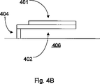
図4Aは、本発明の第2の実施例に従う一部のマイクロミラー素子400の概略平面図である。マイクロミラー401の反射面は、読者の方に面している。マイクロミラー401の反射側は、凹凸のない実質的に平面である。マイクロミラー素子401は、梁402で支えられている。マイクロミラー素子400が空間光変調器(空間光変調器)として配置され、矢印403は素子基板平面上の入射光線伝播方向を示す。そのマイクロミラー401が4つの辺を備えているが、どの辺も矢印403に対して直角でない点に注意する。図4Bは、梁402から線c−dに沿った概略断面図である。梁402は支持構造404で支えられていて、それは素子基板406に配置されている。マイクロミラー301(図3Aおよび3B)とは対照的に、マイクロミラー401の回転軸線は、矢印403とほぼ平行である。
FIG. 4A is a schematic plan view of a portion of a micromirror element 400 according to a second embodiment of the present invention. The reflective surface of the
図5Aは、本発明の第3の実施例によるマイクロミラー素子500の一部の概略平面図である。マイクロミラー501の反射面は、読者に面している。マイクロミラー501の反射する側は、凹凸のない実質的に平面である。マイクロミラー素子500が空間光変調器(空間光変調器)方向の配列に配置されている場合には、矢印503は素子基板平面上の入射光線伝播方向を示す。図5Bは、線e−fに沿った概略断面図である。マイクロミラー501は支持構造504によって支持され、それは素子基板506に配置されている。マイクロミラー501の回転軸線は矢印503とほぼ平行である。
FIG. 5A is a schematic plan view of a part of a
マイクロミラー素子400(図4Aおよび4B)とマイクロミラー素子500(図5Aおよび5B)の間の重要な相違は、素子400においては、支持構造404上に梁402をささえるマイクロミラー401がある一方、素子500では、マイクロミラーは支持構造504上に直接マイクロミラーが配置される。従って、図5Aで支持構造504の頂側部502は、平面的に見える。
An important difference between the micromirror element 400 (FIGS. 4A and 4B) and the micromirror element 500 (FIGS. 5A and 5B) is that in the element 400 there is a micromirror 401 that supports the
図6Aから6Dは、立面図のいろいろなレベルにおける、本発明の第4の実施例に従ったマイクロミラー素子600の概略平面図である。図6Aは、マイクロミラー601の反射する側面(頂側部)である。マイクロミラー素子600が空間光変調器(SLM)方向の配列に配置されている場合には、矢印602は素子基板平面上の入射光線伝播ベクトル方向を示す。矢印602は、マイクロミラー601の4つのどの側面に対しても直角でない。矢印602は、マイクロミラー601の最先端からほぼ45度であることを示す。マイクロミラー601の反射する側面は、凹部も凸部もなく、実質的に平坦である。その結果、マイクロミラーの凹部または凸部によって生じる回折効果はない。
6A to 6D are schematic plan views of a
図6Bは、マイクロミラー601が取り外されたことを除いては、図6Aに類似している平面図である。アドレス電極603および604、マイクロミラー支持構造605およびねじりヒンジ606が見える。ねじりヒンジ606は、マイクロミラー支持構造605を支持する。アドレス電極603および604は、示されていない制御回路に電気的に接続している。マイクロミラー601は、それおよびアドレス電極603および604の一方または両方の間で、静電的な力によって駆動する。図6Cは、ミラー支持構造605を取り外した結果である。
FIG. 6B is a plan view similar to FIG. 6A except that the
図6Dは、ねじりヒンジ606を取り外した結果である。ねじりヒンジ支持構造607および605が、示されている。図7Aから7D、および図8Aから8Mは線g−hに沿って、断面図を使用してマイクロミラー素子の製作順序を示す。多くの場合に、マイクロミラー素子は、空間光変調器としての用途のため製造される。従って、図7Aから7Dおよび図8Aから8Mは、単一のマイクロミラー素子の製作を図示しているが、実際はマイクロミラー素子の配列が製作されることまで拡張されることを理解しなければならない。
FIG. 6D shows the result of removing the
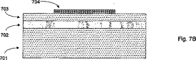
図7Aから7Dは、制御回路側での製作順序を図示する。図7Aはシリコン−オン−絶縁物(SOI)基板700を示しており、この基板は、厚み約775マイクロメートルのシリコン最下層、概50ナノメートルから2マイクロメートルまでの厚みを有する中間絶縁体層702、および概50ナノメートルから600ナノメートルまでの厚みを有するシリコンエピタキシャル最上層703から成る。シリコン基板上のSOIの利点のうちの1つは、優れた誘電隔離性である。本発明の場合、SOI基板が、制御回路とマイクロミラー部の誘電隔離のために用いられている。
7A to 7D illustrate the fabrication sequence on the control circuit side. FIG. 7A shows a silicon-on-insulator (SOI)
図7Bは、SOI基板700のエピタキシャル層703上に制御回路704が形成されるところを示している。一般的に、いかなる集積回路技術も、制御回路の製作のために考慮されることができる。例えば、CMOS回路が用いられることができる。しかしながら、高周波または高電圧が必要な場合では、BiCMOSまたはDMOS回路が、用いられることができる。
FIG. 7B shows that the
図7Cは、標準のパターニングおよび非等方性エッチングを用いて、溝705が表面のエピタキシャル・シリコン層703および絶縁体層702までを形成する工程である。溝705の最下層がシリコン層701に達する前に、非等方性エッチングは止められる。この後に、制御回路と溝の間の電気接続706を形成する金属付着およびパターニング工程(図7D)が続く。この金属として半導体の製作(例えばAl合金)において通常用いられるいかなる金属も可能であると理解されなければならない。そして、金属付着の方法として、スパッタリング、熱蒸着およびCVDがある。
FIG. 7C is a process in which the trench 705 forms up to the surface
この時点で、制御回路側上のプロセス工程は、終了する。保護層を制御回路側の上に形成することが望ましい。図8Aから8Mは、マイクロミラー側上の製作順序を図示する。制御回路側は、次の工程で裏面研磨し化学研磨(CMP)の工程(図8A)をするために、基板を安全に保ちキャリアに設置する。研磨は、中間の絶縁体層702を露出させるためシリコン層に対して行われる。
At this point, the process steps on the control circuit side are complete. It is desirable to form a protective layer on the control circuit side. 8A to 8M illustrate the fabrication sequence on the micromirror side. The control circuit side keeps the substrate safe and is placed on the carrier in order to perform the back surface polishing and chemical polishing (CMP) step (FIG. 8A) in the next step. Polishing is performed on the silicon layer to expose the
図8Bに示すように、絶縁体層702は溝801を形成するためパターン化され、このことにより図7cに始まった経路は完了する。次に金属化(付着およびパターン化)工程(図8C)が行われ、経路801を通過して、制御回路704へ電気的に接続されるアドレス電極802が形成される。
As shown in FIG. 8B, the
アドレス電極802の形成の後、ねじりヒンジおよびその支持構造が形成される。この方法の実施例は、図8Dから8Hにおいて図示される。アモルファスシリコン除去層803は、低圧CVD(LPCVD)(図8D)によって付着される。アモルファスシリコンを付着させる他の適切な方法は、PECVD、触媒CVD(別名ホットワイヤーCVDとして知られている)およびスパッタリングである。背景技術のセクションで述べたように、キセノン・ジフロライドは100〜1の選択性をもってアモルファスシリコンをエッチングするために用いることができる。他の可能な除去層としては、フオトレジスト、シリコン酸化物、窒化シリコンおよびシリコン・オキシ窒化物がある。図8Eに示すように、写真平板パターン化と異方性のエッチング工程は、ねじりヒンジが形成される凹部804を形成するために実行される。それから、次のフォトリソグラフィーによるパターンニングと異方性エッチング工程(図8F)により、ねじりヒンジ支持構造用孔805および806を形成される。ねじりヒンジ支持構造のための孔805および806は、中間の絶縁体層に達する。
After the formation of the
次に、図8Gに示すように、構造材料層807が付着される。この場合、構造材料は、0.2%のTi、1%のSiおよび残りAlから成るAl合金が好ましい。このAl合金を付着させる適した方法は、スパッタ付着である。マイクロミラーが接地電圧で保たれるように、適した金属が構造材料のために選択される。図8Hに示すように、構造材料層807は、ねじりヒンジ808とねじりヒンジ支持構造809および810を形成するためにパターン化される。ねじりヒンジ808とねじりヒンジ支持構造809および810は、除去的層803に少なくとも部分的に埋め込まれている。
Next, as shown in FIG. 8G, a
マイクロミラー支持構造は、ねじり梁とマイクロミラーの間に配置される。図8Iに示すように、金属層が付着し、それから、ねじり梁808上のマイクロミラー支持構造811が得られるようにパターン化される。金属層は、0.2%のTi、1%のSiおよび残りAlから成るAl合金が望ましい。このAl合金を付着させるのに適した方法は、スパッタ付着である。マイクロミラー支持構造811が除去層803によって完全にカバーされるために、アモルファスシリコンによるさらなる付着が行われる(図8J)。次に、ケミカルメカニカルポリシング(CMP)プロセスが表面層を平坦化するために実行される。この際、以下の条件が満たされる必要がある。
1)マイクロミラー支持構造811の上部は、露出していて平面であること、
2)除去的層803は平面であること、そして、
3)マイクロミラー支持構造811の上部および除去的層803の上部は、同じレベルにある。
この明細書において、上部は、図面ページでは一番下を意味する。平坦化工程の結果は、図式的に図8Kに示される。
The micromirror support structure is disposed between the torsion beam and the micromirror. As shown in FIG. 8I, a metal layer is deposited and then patterned to obtain a
1) The upper part of the
2) The
3) The top of the
In this specification, the upper part means the bottom in the drawing page. The result of the planarization process is shown schematically in FIG. 8K.
図8Lに示すようにマイクロミラー812を形成するために、金属層は付着して、パターン化される。金属は0.2%のTi、1%のSiおよび残りがAlから成るAl合金が望ましい。このAl合金を付着させるのに適した方法は、スパッタ付着である。マイクロミラー812は、マイクロミラー支持構造811へ結合されている。キセノン・ジフロライドが、アモルファスシリコン除去層(図8M)をエッチングで取り除くために使われる。
To form the
前述の考察において、適したマイクロミラーは、金属コーティングから出来ていた。しかしながら、高い屈折率と低い屈折率の誘電体層を交互に多層にしたマイクロミラーを製作することもまた可能である。これは、シリコン酸化物および窒化シリコンを用いて作ることができる。従って、Al鏡が92%の反射率を有する場合、最初に68ナノメートルの窒化シリコン(n=2.0)を付着させて、それから96ナノメートルの二酸化ケイ素(n=1.46)を付着させた構造のミラーによって、95%以上の反射率を得ることができる。 In the discussion above, a suitable micromirror was made of a metal coating. However, it is also possible to fabricate a micromirror in which dielectric layers having a high refractive index and a low refractive index are alternately multilayered. This can be made using silicon oxide and silicon nitride. Thus, if the Al mirror has 92% reflectivity, first deposit 68 nanometer silicon nitride (n = 2.0), then deposit 96 nanometer silicon dioxide (n = 1.46). The reflectivity of 95% or more can be obtained by the mirror having the above structure.
図8Gから8Mに関する前述の議論において、構造部材(ねじりヒンジ、ねじりヒンジ支持構造、マイクロミラー、マイクロミラー支持構造)の全ては、金属で出来ていた。しかし、米国特許第5,631,782号に記載されているように、構造部材として金属シースで覆われていた誘電体(例えば硬化したフオトレジスト、シリコン酸化物、窒化シリコン、シリコン・オキシ窒化物)を使用することは可能である。 In the above discussion regarding FIGS. 8G to 8M, all of the structural members (torsion hinge, torsion hinge support structure, micromirror, micromirror support structure) were made of metal. However, as described in US Pat. No. 5,631,782, a dielectric (eg, hardened photoresist, silicon oxide, silicon nitride, silicon oxynitride) covered with a metal sheath is used as a structural member. It is possible.
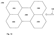
典型例として、マイクロミラー素子は図9に示すように配列される。図9は、本発明の第5の実施例による長方形マイクロミラー(901、902、903および904)の2次元の配列900を示す。矢印906は、鏡平面(素子基板平面)上の入射光線伝播ベクトル方向を示す。マイクロミラーの反射する側では、矢印906に対して直角である辺を有さない。これは、光学システムの受理円錐への回折を減らす構成である。本発明の第6の実施例によれば、マイクロミラーのための他の可能な形状は、六角形(図10の配列1000に配置されて示される)である。ここでは、マイクロミラー1001、1002、1003、1004および1005がある。矢印1006は、鏡平面(素子基板平面)上の入射光線伝播ベクトル方向を示す。マイクロミラーの反射する側は、矢印1006に対して直角である辺を有しない。
As a typical example, the micromirror elements are arranged as shown in FIG. FIG. 9 shows a two-dimensional array 900 of rectangular micromirrors (901, 902, 903 and 904) according to a fifth embodiment of the present invention. An
本発明の第7の実施例は、図11Aおよび11Bを用いて説明される。図11Aはマイクロミラー素子1100の概略平面図であり、マイクロミラー1101およびマイクロミラー支持構造1104から成る。矢印1103は、マイクロミラー平面(素子基板平面)上の入射光線伝播ベクトル方向を示す。マイクロミラーの反射する側は、矢印1103に対して直角である辺を有しない。マイクロミラー1101の反射する側は、凹部も凸部もなく実質的に平面である。図11Bは図11Aの線i−jに沿った概略断面図である。アドレス電極1108はマイクロミラー1101の下に、素子基板1106の上に位置する。さらにまた、ストッパー1107が提供された。ストッパー1107の目的は、偏向によりマイクロミラー1101がアドレス電極1108に接触するのを妨げることである。この接触は、電気ショートの原因になる。その代わりに、マイクロミラー1101はストッパー1107と接触する。マイクロミラーが偏向していない状態から、2方向において偏向する場合、各々の方向の偏向のために1つずつ用意し、2つのストッパーを提供することができる。
A seventh embodiment of the present invention will be described with reference to FIGS. 11A and 11B. FIG. 11A is a schematic plan view of the
図11cは、本発明の第8の実施例に係るマイクロミラー素子1100を図示する。図11Cは、マイクロミラー素子1100の平面図であり、マイクロミラー1101、支持構造1104およびストッパー1107から成る。偏向していない状態において、マイクロミラー1101の反射面の辺は、矢印1103に対して直角である辺を有さない。マイクロミラー1101が駆動すると、支持構造1104に結合しているマイクロミラー1101のミラー領域1108は偏向する。従って、矢印1103に対して直角である辺は、領域1108に現れることがありうる。この辺からの回折効果を減らすために、領域1108を光吸収材料で被覆することは、可能である。好適な光吸収材料は、黒い染料である。
FIG. 11c illustrates a
Claims (3)
Applications Claiming Priority (2)
| Application Number | Priority Date | Filing Date | Title |
|---|---|---|---|
| US10/698,620 US20050094241A1 (en) | 2003-11-01 | 2003-11-01 | Electromechanical micromirror devices and methods of manufacturing the same |
| PCT/US2004/035974 WO2005046206A2 (en) | 2003-11-01 | 2004-10-29 | Electromechanical micromirror devices and methods of manufacturing the same |
Publications (3)
| Publication Number | Publication Date |
|---|---|
| JP2007510954A JP2007510954A (en) | 2007-04-26 |
| JP2007510954A5 JP2007510954A5 (en) | 2008-01-10 |
| JP4586146B2 true JP4586146B2 (en) | 2010-11-24 |
Family
ID=34550697
Family Applications (1)
| Application Number | Title | Priority Date | Filing Date |
|---|---|---|---|
| JP2006538296A Expired - Fee Related JP4586146B2 (en) | 2003-11-01 | 2004-10-29 | Electrodynamic micromirror device and method for manufacturing the same |
Country Status (3)
| Country | Link |
|---|---|
| US (3) | US20050094241A1 (en) |
| JP (1) | JP4586146B2 (en) |
| WO (1) | WO2005046206A2 (en) |
Families Citing this family (16)
| Publication number | Priority date | Publication date | Assignee | Title |
|---|---|---|---|---|
| US7643195B2 (en) * | 2003-11-01 | 2010-01-05 | Silicon Quest Kabushiki-Kaisha | Mirror device |
| US7777959B2 (en) * | 2004-05-27 | 2010-08-17 | Angstrom, Inc. | Micromirror array lens with fixed focal length |
| US7864394B1 (en) * | 2005-08-31 | 2011-01-04 | The United States Of America As Represented By The Secretary Of The Navy | Dynamically variable metamaterial lens and method |
| US7691400B2 (en) * | 2006-05-05 | 2010-04-06 | Medtronic Vascular, Inc. | Medical device having coating with zeolite drug reservoirs |
| US7652813B2 (en) * | 2006-08-30 | 2010-01-26 | Silicon Quest Kabushiki-Kaisha | Mirror device |
| US8023172B2 (en) * | 2006-08-30 | 2011-09-20 | Silicon Quest Kabushiki-Kaisha | Mirror device |
| US7863752B2 (en) * | 2009-02-25 | 2011-01-04 | Capella Photonics, Inc. | MEMS device with integrated via and spacer |
| US8040590B2 (en) * | 2009-10-29 | 2011-10-18 | Qualcomm Mems Technologies, Inc. | Interferometric modulation devices having triangular subpixels |
| JP2013530418A (en) | 2010-04-28 | 2013-07-25 | レモプティックス ソシエテ アノニム | Microprojection device with anti-speckle imaging mode |
| US8654435B2 (en) * | 2010-10-06 | 2014-02-18 | Fusao Ishii | Microwindow device |
| EP2447755B1 (en) | 2010-10-26 | 2019-05-01 | Lumentum Operations LLC | A pivotable MEMS device |
| WO2014168658A1 (en) * | 2013-04-09 | 2014-10-16 | Fusao Ishii | Mirror device with flat and smooth mirror surface without protrusion or dip |
| US9429760B2 (en) * | 2014-10-07 | 2016-08-30 | Christie Digital Systems Usa, Inc. | Spatial color mixing in a cascade imaging system |
| WO2020069482A1 (en) * | 2018-09-29 | 2020-04-02 | Ignite, Inc. | A mems display device with a vertical hinge |
| CN111491144B (en) * | 2019-01-28 | 2023-04-07 | 深圳光峰科技股份有限公司 | Display method, display system and computer storage medium |
| US11668925B2 (en) * | 2020-03-25 | 2023-06-06 | Compertum Microsystems Inc. | MEMS micro-mirror device with stopper and method of making same |
Family Cites Families (27)
| Publication number | Priority date | Publication date | Assignee | Title |
|---|---|---|---|---|
| US4229782A (en) * | 1977-12-20 | 1980-10-21 | Mcgraw-Edison Company | High efficiency lighting units with beam cut-off angle |
| US4317611A (en) * | 1980-05-19 | 1982-03-02 | International Business Machines Corporation | Optical ray deflection apparatus |
| US4592628A (en) * | 1981-07-01 | 1986-06-03 | International Business Machines | Mirror array light valve |
| US5061049A (en) * | 1984-08-31 | 1991-10-29 | Texas Instruments Incorporated | Spatial light modulator and method |
| US4662746A (en) * | 1985-10-30 | 1987-05-05 | Texas Instruments Incorporated | Spatial light modulator and method |
| US5216537A (en) * | 1990-06-29 | 1993-06-01 | Texas Instruments Incorporated | Architecture and process for integrating DMD with control circuit substrates |
| US5583688A (en) * | 1993-12-21 | 1996-12-10 | Texas Instruments Incorporated | Multi-level digital micromirror device |
| US5535047A (en) * | 1995-04-18 | 1996-07-09 | Texas Instruments Incorporated | Active yoke hidden hinge digital micromirror device |
| US6046840A (en) * | 1995-06-19 | 2000-04-04 | Reflectivity, Inc. | Double substrate reflective spatial light modulator with self-limiting micro-mechanical elements |
| US5835256A (en) * | 1995-06-19 | 1998-11-10 | Reflectivity, Inc. | Reflective spatial light modulator with encapsulated micro-mechanical elements |
| KR100243190B1 (en) * | 1996-06-10 | 2000-02-01 | 윤종용 | Movable mirror array and its fabrication method |
| KR100635589B1 (en) * | 1998-09-24 | 2006-10-18 | 리플렉티버티 인코퍼레이티드 | A double substrate reflective spatial light modulator with self-limiting micro-mechanical elements and a method for manufacturing the same |
| US6323834B1 (en) * | 1998-10-08 | 2001-11-27 | International Business Machines Corporation | Micromechanical displays and fabrication method |
| US6266178B1 (en) * | 1998-12-28 | 2001-07-24 | Texas Instruments Incorporated | Guardring DRAM cell |
| US6935023B2 (en) * | 2000-03-08 | 2005-08-30 | Hewlett-Packard Development Company, L.P. | Method of forming electrical connection for fluid ejection device |
| US6639713B2 (en) * | 2000-04-25 | 2003-10-28 | Umachines, Inc. | Silicon micromachined optical device |
| US6867897B2 (en) * | 2003-01-29 | 2005-03-15 | Reflectivity, Inc | Micromirrors and off-diagonal hinge structures for micromirror arrays in projection displays |
| US6873450B2 (en) * | 2000-08-11 | 2005-03-29 | Reflectivity, Inc | Micromirrors with mechanisms for enhancing coupling of the micromirrors with electrostatic fields |
| US6576496B1 (en) * | 2000-08-21 | 2003-06-10 | Micron Technology, Inc. | Method and apparatus for encapsulating a multi-chip substrate array |
| JP4360582B2 (en) * | 2000-10-31 | 2009-11-11 | 京セラ株式会社 | Package for storing digital micromirror devices |
| FR2820833B1 (en) * | 2001-02-15 | 2004-05-28 | Teem Photonics | PIVOT OPTICAL MICRO-MIRROR, MATRIX OF SUCH MICRO-MIRRORS AND METHOD FOR PRODUCING THE SAME |
| US6922499B2 (en) * | 2001-07-24 | 2005-07-26 | Lucent Technologies Inc. | MEMS driver circuit arrangement |
| US6838302B2 (en) * | 2002-01-11 | 2005-01-04 | Reflectivity, Inc | Method for adjusting a micro-mechanical device |
| JP2004130507A (en) * | 2002-09-19 | 2004-04-30 | Nippon Telegr & Teleph Corp <Ntt> | Electronic component device |
| US6914711B2 (en) * | 2003-03-22 | 2005-07-05 | Active Optical Networks, Inc. | Spatial light modulator with hidden comb actuator |
| US6903860B2 (en) * | 2003-11-01 | 2005-06-07 | Fusao Ishii | Vacuum packaged micromirror arrays and methods of manufacturing the same |
| US7183618B2 (en) * | 2004-08-14 | 2007-02-27 | Fusao Ishii | Hinge for micro-mirror devices |
-
2003
- 2003-11-01 US US10/698,620 patent/US20050094241A1/en not_active Abandoned
-
2004
- 2004-10-29 WO PCT/US2004/035974 patent/WO2005046206A2/en active Application Filing
- 2004-10-29 JP JP2006538296A patent/JP4586146B2/en not_active Expired - Fee Related
-
2005
- 2005-07-23 US US11/187,248 patent/US7375872B2/en active Active
-
2008
- 2008-02-12 US US12/069,837 patent/US7746538B2/en not_active Expired - Fee Related
Also Published As
| Publication number | Publication date |
|---|---|
| US20050094241A1 (en) | 2005-05-05 |
| US20060018005A1 (en) | 2006-01-26 |
| US7746538B2 (en) | 2010-06-29 |
| WO2005046206A3 (en) | 2006-05-18 |
| US20080180778A1 (en) | 2008-07-31 |
| WO2005046206A2 (en) | 2005-05-19 |
| JP2007510954A (en) | 2007-04-26 |
| US7375872B2 (en) | 2008-05-20 |
Similar Documents
| Publication | Publication Date | Title |
|---|---|---|
| US6862127B1 (en) | High performance micromirror arrays and methods of manufacturing the same | |
| JP4586146B2 (en) | Electrodynamic micromirror device and method for manufacturing the same | |
| JP4545153B2 (en) | Micromirror array element packaged in vacuum and manufacturing method thereof | |
| EP1509802B1 (en) | Bulk silicon mirrors with hinges underneath | |
| US7394586B2 (en) | Spatial light modulator | |
| US6379510B1 (en) | Method of making a low voltage micro-mirror array light beam switch | |
| US6528887B2 (en) | Conductive equipotential landing pads formed on the underside of a MEMS device | |
| US7428092B2 (en) | Fast-response micro-mechanical devices | |
| US20060082250A1 (en) | Biaxial actuator and method of manufacturing the same | |
| US8724200B1 (en) | MEMS hierarchically-dimensioned optical mirrors and methods for manufacture thereof | |
| US20020167072A1 (en) | Electrostatically actuated micro-electro-mechanical devices and method of manufacture | |
| US6876484B2 (en) | Deformable segmented MEMS mirror | |
| JPH05257070A (en) | Silicon spatial light modulator | |
| KR100579868B1 (en) | Micro mirror and method for fabricating thereof | |
| US8908255B2 (en) | Fabrication of a high fill ratio silicon spatial light modulator | |
| US20020064337A1 (en) | MEMS mirrors with precision clamping mechanism | |
| JP2013068678A (en) | Optical deflector and optical deflector array | |
| WO2001094253A2 (en) | Bulk silicon structures with thin film flexible elements | |
| JP2008209616A (en) | Optical deflector and method of manufacturing the same | |
| JPH07301755A (en) | M x n pieces of thin-film actuated mirror array and manufacture thereof | |
| KR100404195B1 (en) | micro mirror and method for fabricating micro mirror | |
| KR100276663B1 (en) | Manufacturing method of thin film type optical path control device | |
| KR100276664B1 (en) | Thin film type optical path control device and its manufacturing method | |
| EP2211223A1 (en) | Method for generating a deflectable mirror structure and a micromirror device | |
| KR20000044211A (en) | Thin film micromirror array-actuated device and manufacturing method |
Legal Events
| Date | Code | Title | Description |
|---|---|---|---|
| A521 | Written amendment |
Free format text: JAPANESE INTERMEDIATE CODE: A523 Effective date: 20060510 |
|
| A521 | Written amendment |
Free format text: JAPANESE INTERMEDIATE CODE: A523 Effective date: 20061115 |
|
| A521 | Written amendment |
Free format text: JAPANESE INTERMEDIATE CODE: A523 Effective date: 20061213 |
|
| A521 | Written amendment |
Free format text: JAPANESE INTERMEDIATE CODE: A523 Effective date: 20071029 |
|
| A621 | Written request for application examination |
Free format text: JAPANESE INTERMEDIATE CODE: A621 Effective date: 20071029 |
|
| A521 | Written amendment |
Free format text: JAPANESE INTERMEDIATE CODE: A523 Effective date: 20071029 |
|
| A131 | Notification of reasons for refusal |
Free format text: JAPANESE INTERMEDIATE CODE: A131 Effective date: 20100126 |
|
| A521 | Written amendment |
Free format text: JAPANESE INTERMEDIATE CODE: A523 Effective date: 20100426 |
|
| A131 | Notification of reasons for refusal |
Free format text: JAPANESE INTERMEDIATE CODE: A131 Effective date: 20100601 |
|
| A521 | Written amendment |
Free format text: JAPANESE INTERMEDIATE CODE: A523 Effective date: 20100629 |
|
| TRDD | Decision of grant or rejection written | ||
| A01 | Written decision to grant a patent or to grant a registration (utility model) |
Free format text: JAPANESE INTERMEDIATE CODE: A01 Effective date: 20100714 |
|
| A01 | Written decision to grant a patent or to grant a registration (utility model) |
Free format text: JAPANESE INTERMEDIATE CODE: A01 |
|
| A61 | First payment of annual fees (during grant procedure) |
Free format text: JAPANESE INTERMEDIATE CODE: A61 Effective date: 20100806 |
|
| R150 | Certificate of patent or registration of utility model |
Free format text: JAPANESE INTERMEDIATE CODE: R150 |
|
| FPAY | Renewal fee payment (event date is renewal date of database) |
Free format text: PAYMENT UNTIL: 20130917 Year of fee payment: 3 |
|
| LAPS | Cancellation because of no payment of annual fees |