JP4579552B2 - Infrared display device - Google Patents
Infrared display device Download PDFInfo
- Publication number
- JP4579552B2 JP4579552B2 JP2004022347A JP2004022347A JP4579552B2 JP 4579552 B2 JP4579552 B2 JP 4579552B2 JP 2004022347 A JP2004022347 A JP 2004022347A JP 2004022347 A JP2004022347 A JP 2004022347A JP 4579552 B2 JP4579552 B2 JP 4579552B2
- Authority
- JP
- Japan
- Prior art keywords
- infrared
- light emitting
- display
- circuit
- infrared light
- Prior art date
- Legal status (The legal status is an assumption and is not a legal conclusion. Google has not performed a legal analysis and makes no representation as to the accuracy of the status listed.)
- Expired - Fee Related
Links
Images


Landscapes
- Control Of El Displays (AREA)
- Control Of Indicators Other Than Cathode Ray Tubes (AREA)
Description
本発明は、赤外線LED(Light Emitting Diode)を用いたディスプレイ装置に係り、表示と通信を同時に行うことができる技術に関する。 The present invention relates to a display device using an infrared LED (Light Emitting Diode), and relates to a technique capable of simultaneously performing display and communication.
赤外発光ダイオードを用いたディスプレイ装置について、特開平9−127913号公報の[0049]に、各画素の発光サイドに赤、緑、青のLEDに加えて赤外線発光ダイオードを入れる技術が開示されている。当該技術は、普通の画像データに重畳させて、他の画像データを表示させたり、高配列の光通信に使用することを想定している。 Regarding a display device using infrared light emitting diodes, [0049] of Japanese Patent Application Laid-Open No. 9-127913 discloses a technique for placing an infrared light emitting diode in addition to red, green and blue LEDs on the light emitting side of each pixel. Yes. This technology assumes that other image data is displayed by superimposing on normal image data, or is used for high-order optical communication.
しかし、この例では、画像データの表示あるいは光通信を、個別に行うことを想定しており、表示と通信を同時に行うようにする技術については、開示されていない。
本発明は、上記した従来技術の欠点を除くためになされたものであって、その目的とするところは、赤外線LEDを用いたディスプレイ装置に係り、表示と通信を同時に行うことができるようにすることを課題とする。 The present invention has been made to eliminate the above-described drawbacks of the prior art, and an object of the present invention relates to a display device using an infrared LED so that display and communication can be performed simultaneously. This is the issue.
本発明に係る赤外線ディスプレイ装置は、
以下の要素を有することを特徴とする
(1)ディスプレイにおける可視状態を想定して変化する表示情報を、画素当たりの表示あるいは非表示に随時割り当てた表示情報回路出力データを出力する表示情報回路
(2)赤外線通信に係る送信のパルス波形を示すデータ通信回路出力データを出力するデータ通信回路
(3)前記表示情報回路出力データと前記データ通信回路出力データの論理積を生成し、点灯信号として出力する論理積回路
(4)前記点灯信号に従って赤外線発光素子を発光させる赤外線発光素子入力信号を出力するドライブ回路
(5)赤外線発光素子入力信号により赤外線を発光する赤外線発光素子。
Infrared display device according to the present invention,
(1) A display information circuit that outputs display information circuit output data that is assigned to display or non-display per pixel as needed, and that changes display information assuming a visible state on the display. 2) Data communication circuit that outputs data communication circuit output data indicating a pulse waveform of transmission related to infrared communication (3) Generates a logical product of the display information circuit output data and the data communication circuit output data, and outputs it as a lighting signal AND circuit (4) A drive circuit for outputting an infrared light emitting element input signal for causing the infrared light emitting element to emit light in accordance with the lighting signal. (5) An infrared light emitting element for emitting infrared light by the infrared light emitting element input signal.
本発明により、赤外線による表示と通信を同時に行える赤外線ディスプレイ装置が実現できる。 According to the present invention, an infrared display device capable of simultaneously performing infrared display and communication can be realized.
実施の形態1.
以下本発明を図面に示す実施例に基づいて説明する。本発明に係る赤外線ディスプレイ装置は、複数画素から構成されている。まず、1画素当たりの構成について説明する。図1は、1画素当たりの構成を示す図である。表示情報回路1、データ通信回路2、AND回路(論理積回路)3、ドライブ回路4、赤外線発光ダイオード5から構成されている。
Embodiment 1 FIG.
Hereinafter, the present invention will be described based on embodiments shown in the drawings. The infrared display device according to the present invention is composed of a plurality of pixels. First, the configuration per pixel will be described. FIG. 1 is a diagram illustrating a configuration per pixel. The display information circuit 1, the
表示情報回路1は、ディスプレイにおける可視状態を想定して変化する表示情報を、画素当たりの表示指示(ON)あるいは非表示指示(OFF)に随時割り当てたデータを出力するように構成されている。このデータを、表示情報回路出力データと呼ぶ。例えば、上記表示情報を入力し、各画素に割り当てる構成となる。 The display information circuit 1 is configured to output data in which display information that changes assuming a visible state on the display is assigned to a display instruction per pixel (ON) or non-display instruction (OFF) as needed. This data is called display information circuit output data. For example, the display information is input and assigned to each pixel.
図2は、各信号を示す図である。表示情報回路出力データ6は、この表示情報回路出力データを示している。 FIG. 2 is a diagram illustrating each signal. The display information circuit output data 6 indicates the display information circuit output data.
データ通信回路2は、赤外線通信に係る送信用のパルス波形のデータを出力するように構成されている。このデータを、データ通信回路出力データと呼ぶ。図2のデータ通信回路出力データ7は、このデータ通信回路出力データを示している。この回路は、例えば、送信対象の情報を入力し、その情報を上記送信用のパルス波形のデータに変換する。
The
AND回路(論理積回路)3は、表示情報回路出力データとデータ通信回路出力データを入力し、論理積に係るデータを出力するように構成されている。この信号を点灯信号と呼ぶ。図2の点灯信号8は、この点灯信号を示している。
The AND circuit (logical product circuit) 3 is configured to input the display information circuit output data and the data communication circuit output data and output data related to the logical product. This signal is called a lighting signal. A
ドライブ回路4は、電流を供給する回路であり、電源供給源と接続している。ドライブ回路4は、点灯信号を入力し、点灯信号に従ってダイオード入力信号を出力するように構成されている。つまり、点灯信号と同期してダイオードを発光させる電流を出力する。
The
赤外線発光ダイオード5は、赤外線を発光するLED素子であり、ダイオード入力信号により発光するように構成されている。赤外線発光素子の例である。
The infrared
図3は、複数画素の構成を示す図である。表示情報回路1は、画素毎に固有の表示情報回路出力データを出力し、それぞれのAND回路(論理積回路)3−1〜Nに供給される。データ通信回路2は、共通のデータ通信回路出力データを、すべてのAND回路(論理積回路)3−1〜Nに供給する。
FIG. 3 is a diagram illustrating a configuration of a plurality of pixels. The display information circuit 1 outputs display information circuit output data unique to each pixel, and is supplied to each AND circuit (logical product circuit) 3-1 to N. The
このように構成することにより、ディスプレイ全体として可視状態を想定した点灯の制御を行うと同時に、赤外線通信に係るパルス波を点灯中の画素から送信することができる。 By configuring in this way, it is possible to perform lighting control assuming a visible state as the entire display, and at the same time, it is possible to transmit a pulse wave related to infrared communication from a pixel that is lit.
赤外線は、肉眼では認識できないが、携帯電話の付属カメラ、デジタルカメラ、あるいはビデオカメラなどの受光装置で受光したデータを表示装置で表示させると、白色の光として肉眼で認識できるようになる。その為、例えば、携帯電話のカメラと表示装置を介して、可視状態を想定した表示状態を読み取ることができるようになる。 Infrared rays cannot be recognized with the naked eye, but when data received by a light receiving device such as a camera attached to a cellular phone, a digital camera, or a video camera is displayed on a display device, it can be recognized with white light as white light. Therefore, for example, a display state assuming a visible state can be read through a camera of a mobile phone and a display device.
図4は、ディスプレイの適用形態を示す図である。41は、通常用いられる可視光によるディスプレイ装置である。42は、本発明に係る赤外線ディスプレイ装置である。例えば、競馬場の表示システムとして本装置を用いる場合には、競走馬の映像を可視ディスプレイ装置41に表示し、同時に当該競走馬の名前等の基本情報を、赤外線ディスプレイ装置42の表示情報として出力することが考えられる。利用者は、可視ディスプレイ装置41に表示されている競走馬の名前等を確認したい場合に、携帯電話のカメラを起動させ、赤外線ディスプレイ装置42からの赤外線を受光することにより、当該名前を携帯電話の表示装置で確認することができる。
FIG. 4 is a diagram showing an application form of the display.
また、赤外線ディスプレイ装置42は同時に赤外線通信に係るパルス波を出力している。従って、携帯電話43で赤外線を受信することにより、当該競走馬に係る詳細情報等を受信し、携帯電話の表示アプリケーションで確認することができる。図5は、携帯電話の構成を示す図である。IrDA(Infrared Data Association)受信モジュール51で、赤外通信に係る受信処理を行い、アプリケーション用マイコン52で動作するアプリケーションソフトにより受信したデータを表示装置に出力する。
Further, the
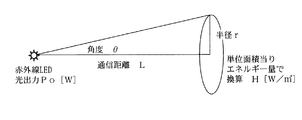
ここで、赤外通信を行うための条件について簡単な試算を示す。図6は、受光エネルギーの概要を示す図である。 Here, a simple trial calculation will be given regarding the conditions for performing infrared communication. FIG. 6 is a diagram showing an outline of received light energy.
単位面積当りのエネルギー量Hを数式で表す。
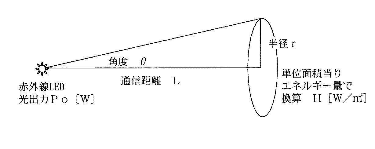
赤外線LEDをN個使用した場合には、N倍となる。
リモコン装置の通信状況から推測する。受信モジュールにおけるノイズ源は、太陽光などの他の光源が主である。したがって,リモコンを晴天昼時に外で使用する場合を想定する。リモコンを晴天昼時に外で使用し、最大通信距離を3m程度、赤外線LEDパルス光出力を200mW、指向特性を±15度とすると、H=98.52 mW/m2となる。 Inferred from the communication status of the remote control device. The noise source in the receiving module is mainly other light sources such as sunlight. Therefore, it is assumed that the remote control is used outside on a sunny day. If the remote control is used outside in the daytime on a fine day, the maximum communication distance is about 3 m, the infrared LED pulse light output is 200 mW, and the directivity is ± 15 degrees, then H = 98.52 mW / m 2 .
外で晴天昼時の仕様を想定した場合の最小受信エネルギー量をH=100mW/m2、赤外線LEDパルス光出力を200mW、指向特性を±30度とすると、通信距離50mを確保するためには,赤外線LEDを1500個以上全点灯する必要が有る。尚、一般的にはLEDディスプレイの1素子は複数個のLED素子をまとめたもの(1LED素子で十分な光量は出せないため)であり、例えば5個のLED素子を1画素子とした場合には、実際には300個以上の画素を発光させることにより、赤外線通信が可能になる。 In order to secure a communication distance of 50 m, assuming that the minimum received energy amount is H = 100 mW / m 2 , the infrared LED pulsed light output is 200 mW, and the directivity is ± 30 degrees, assuming the specifications for sunny daytime outside. , It is necessary to light all 1500 or more infrared LEDs. In general, one element of an LED display is a group of a plurality of LED elements (because a single LED element cannot produce a sufficient amount of light). In fact, infrared communication becomes possible by emitting light from 300 or more pixels.
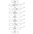
最後に、携帯電話側のアプリケーションの例について説明する。図7は、アプリケーションのフローを示す図である。 Finally, an example of an application on the mobile phone side will be described. FIG. 7 is a diagram illustrating a flow of an application.
まず、本アプリケーションを立ち上げる(S71)。これにより、カメラの機能が起動し、携帯電話の表示装置で赤外線ディスプレイ装置42の表示を読み取ることができるようになる。そして、メニューから「競走馬の選択」の項目を選択すると(S72)、カメラの機能を停止させ、赤外線通信に係る受信機能を起動する。そして、この状態で登録ボタンが押されると(S73)、赤外線通信による受信を行う。この例では、競走馬の馬番を受信する。一旦、登録を終了し(S74)、インターネットによる通信を開始する(S75)。そして、先に受信した馬番に係るオッズ等の情報を取得し(S76)、通信を終了する(S77)。
First, this application is started up (S71). Thereby, the function of the camera is activated, and the display on the
このアプリケーションは一例に過ぎず、さまざまな応用が考えられる。 This application is only an example, and various applications are possible.
実施の形態2.
上述の赤外線に係る発光素子は、可視光に係る発光素子と組み合せて画素を構成するようにしてもよい。例えば、三原色のLED群に赤外線LEDを加えて、画素を構成するディスプレイが考えられる。
The above-described infrared light-emitting element may be combined with a visible light-emitting element to form a pixel. For example, a display in which a pixel is configured by adding an infrared LED to a group of three primary color LEDs can be considered.
1 表示情報回路、2 データ通信回路、3 AND回路(論理積回路)、4 ドライブ回路、5 赤外線発光ダイオード、6 表示情報回路出力データ、7 データ通信回路出力データ、8 点灯信号、41 可視ディスプレイ装置、42 赤外線ディスプレイ装置、43 携帯電話、51 IrDA受信モジュール、52 アプリケーション用マイコン、53 通信用マイコン。 DESCRIPTION OF SYMBOLS 1 Display information circuit, 2 Data communication circuit, 3 AND circuit (logical product circuit), 4 Drive circuit, 5 Infrared light emitting diode, 6 Display information circuit output data, 7 Data communication circuit output data, 8 Lighting signal, 41 Visible display device , 42 Infrared display device, 43 mobile phone, 51 IrDA receiving module, 52 application microcomputer, 53 communication microcomputer.
Claims (2)
赤外線通信に係る送信のパルス波形を示すデータ通信回路出力データを出力するデータ通信回路と、
前記表示情報回路出力データと前記データ通信回路出力データの論理積を生成し、点灯信号として出力する論理積回路と、
前記点灯信号に従って赤外線発光素子を発光させる赤外線発光素子入力信号を出力するドライブ回路と、
前記赤外線発光素子入力信号により赤外線を発光する赤外線発光素子とを備え、
前記赤外線発光素子は、可視光に係る発光素子と組み合せて画素を構成する
ことを特徴とする赤外線ディスプレイ装置。 The display information changing assuming visible in de Isupurei, a display information circuit for outputting display information circuit output data assigned at any time to display or hide per pixel,
A data communication circuit that outputs a data communication circuit output data indicating the pulse waveform of the transmission according to the infrared communication,
Generates a logical product of the previous SL display information circuit output data the data communications circuit output data, a logical product circuit for outputting a lighting signal,
A drive circuit for outputting an infrared light-emitting element input signal for emitting an infrared light emitting device according to the previous SL lighting signal,
And an infrared light emitting device that emits infrared rays before Symbol infrared light emitting element input signal,
The infrared light emitting element is combined with a light emitting element related to visible light to form a pixel.
An infrared display device.
Priority Applications (1)
| Application Number | Priority Date | Filing Date | Title |
|---|---|---|---|
| JP2004022347A JP4579552B2 (en) | 2004-01-30 | 2004-01-30 | Infrared display device |
Applications Claiming Priority (1)
| Application Number | Priority Date | Filing Date | Title |
|---|---|---|---|
| JP2004022347A JP4579552B2 (en) | 2004-01-30 | 2004-01-30 | Infrared display device |
Publications (2)
| Publication Number | Publication Date |
|---|---|
| JP2005215360A JP2005215360A (en) | 2005-08-11 |
| JP4579552B2 true JP4579552B2 (en) | 2010-11-10 |
Family
ID=34905724
Family Applications (1)
| Application Number | Title | Priority Date | Filing Date |
|---|---|---|---|
| JP2004022347A Expired - Fee Related JP4579552B2 (en) | 2004-01-30 | 2004-01-30 | Infrared display device |
Country Status (1)
| Country | Link |
|---|---|
| JP (1) | JP4579552B2 (en) |
Cited By (1)
| Publication number | Priority date | Publication date | Assignee | Title |
|---|---|---|---|---|
| US9917143B2 (en) | 2016-02-12 | 2018-03-13 | Samsung Display Co., Ltd. | Organic light emitting diode display |
Families Citing this family (4)
| Publication number | Priority date | Publication date | Assignee | Title |
|---|---|---|---|---|
| JP5468914B2 (en) * | 2010-01-19 | 2014-04-09 | 三菱電機株式会社 | Control device for large video display device |
| KR101198656B1 (en) * | 2011-01-13 | 2012-11-12 | 김태정 | Display apparatus and method using lights in invisible spectrum |
| JP2019507899A (en) * | 2016-01-21 | 2019-03-22 | スリーエム イノベイティブ プロパティズ カンパニー | Optical camouflage filter |
| KR20210143835A (en) * | 2019-03-29 | 2021-11-29 | 베스텔 일렉트로닉 사나이 베 티카레트 에이에스 | A display screen and a processing device for driving the display screen and an operating method thereof |
Family Cites Families (6)
| Publication number | Priority date | Publication date | Assignee | Title |
|---|---|---|---|---|
| US4724356A (en) * | 1986-10-10 | 1988-02-09 | Lockheed Missiles & Space Co., Inc. | Infrared display device |
| US4859080A (en) * | 1988-07-22 | 1989-08-22 | Ssg, Inc. | Dynamic thermal display simulator |
| US5214292A (en) * | 1991-08-14 | 1993-05-25 | Mission Research Corporation | Dynamic infrared scene display |
| JP2617845B2 (en) * | 1992-01-27 | 1997-06-04 | スタンレー電気株式会社 | Light emitting display |
| JPH0969816A (en) * | 1995-08-31 | 1997-03-11 | Sony Corp | Optical communication device |
| EP1062650B1 (en) * | 1998-03-20 | 2008-02-27 | Versitech Ltd. | Tricolor led display system having audio output |
-
2004
- 2004-01-30 JP JP2004022347A patent/JP4579552B2/en not_active Expired - Fee Related
Cited By (2)
| Publication number | Priority date | Publication date | Assignee | Title |
|---|---|---|---|---|
| US9917143B2 (en) | 2016-02-12 | 2018-03-13 | Samsung Display Co., Ltd. | Organic light emitting diode display |
| US10269876B2 (en) | 2016-02-12 | 2019-04-23 | Samsung Display Co., Ltd. | Organic light emitting diode display |
Also Published As
| Publication number | Publication date |
|---|---|
| JP2005215360A (en) | 2005-08-11 |
Similar Documents
| Publication | Publication Date | Title |
|---|---|---|
| EP2422586B1 (en) | Lighting techniques for wirelessly controlling lighting elements | |
| US10103810B2 (en) | Signboard apparatus and signboard system | |
| US20160020854A1 (en) | System to enable communication, sometimes called Li-Fi or Visible Light Communication ( V.L.C. ) between computers or broadcast programs and simple microcontroller gadgets with limited user interfaces, to further the "internet of things" | |
| CN107135567B (en) | Light emission control system | |
| US9766533B2 (en) | Flash device, and imaging method | |
| JP6933862B2 (en) | Light adjustment system and lights | |
| JP2015510302A (en) | Flicker-free color visible light communication system | |
| JP4579552B2 (en) | Infrared display device | |
| AU2010239669B2 (en) | Lighting techniques for wirelessly controlling lighting elements | |
| JP2009130725A (en) | Visible light communication system and optical receiver | |
| JP2006174120A (en) | Information providing apparatus and portable terminal | |
| CN113475090A (en) | Visual digital decoration device and control method thereof | |
| KR102306004B1 (en) | Flexible display device and cheering system using the same | |
| JP2009218898A (en) | Visible light communication system | |
| CN106209229B (en) | Light-based data transmission device and method | |
| US9818319B2 (en) | Wearable device and control method thereof | |
| JP4037817B2 (en) | LCD display screen color adjustment system and method for portable terminal | |
| TW201438508A (en) | Lighting system | |
| CN1627343A (en) | Light show ASIC | |
| KR200347096Y1 (en) | A display device with Light Emitting Diode of a portable phone | |
| JP2010181657A (en) | Display using infrared radiation, and display system using the display | |
| JP2007259470A (en) | Portable device | |
| CN206164990U (en) | Circuit board, camera and image acquisition system | |
| JP2004128831A (en) | Remote controller | |
| HK1162233B (en) | Lighting techniques for wirelessly controlling lighting elements |
Legal Events
| Date | Code | Title | Description |
|---|---|---|---|
| A621 | Written request for application examination |
Free format text: JAPANESE INTERMEDIATE CODE: A621 Effective date: 20070124 |
|
| A131 | Notification of reasons for refusal |
Free format text: JAPANESE INTERMEDIATE CODE: A131 Effective date: 20100518 |
|
| A521 | Request for written amendment filed |
Free format text: JAPANESE INTERMEDIATE CODE: A523 Effective date: 20100621 |
|
| A131 | Notification of reasons for refusal |
Free format text: JAPANESE INTERMEDIATE CODE: A131 Effective date: 20100713 |
|
| A521 | Request for written amendment filed |
Free format text: JAPANESE INTERMEDIATE CODE: A523 Effective date: 20100804 |
|
| TRDD | Decision of grant or rejection written | ||
| A01 | Written decision to grant a patent or to grant a registration (utility model) |
Free format text: JAPANESE INTERMEDIATE CODE: A01 Effective date: 20100824 |
|
| A01 | Written decision to grant a patent or to grant a registration (utility model) |
Free format text: JAPANESE INTERMEDIATE CODE: A01 |
|
| A61 | First payment of annual fees (during grant procedure) |
Free format text: JAPANESE INTERMEDIATE CODE: A61 Effective date: 20100826 |
|
| FPAY | Renewal fee payment (event date is renewal date of database) |
Free format text: PAYMENT UNTIL: 20130903 Year of fee payment: 3 |
|
| R150 | Certificate of patent or registration of utility model |
Free format text: JAPANESE INTERMEDIATE CODE: R150 |
|
| R250 | Receipt of annual fees |
Free format text: JAPANESE INTERMEDIATE CODE: R250 |
|
| LAPS | Cancellation because of no payment of annual fees |