JP4573352B2 - Center-fed waveguide terminated power divider - Google Patents
Center-fed waveguide terminated power divider Download PDFInfo
- Publication number
- JP4573352B2 JP4573352B2 JP2005042053A JP2005042053A JP4573352B2 JP 4573352 B2 JP4573352 B2 JP 4573352B2 JP 2005042053 A JP2005042053 A JP 2005042053A JP 2005042053 A JP2005042053 A JP 2005042053A JP 4573352 B2 JP4573352 B2 JP 4573352B2
- Authority
- JP
- Japan
- Prior art keywords
- waveguide
- feed
- radiating
- radiation
- feeding
- Prior art date
- Legal status (The legal status is an assumption and is not a legal conclusion. Google has not performed a legal analysis and makes no representation as to the accuracy of the status listed.)
- Active
Links
Images


Landscapes
- Waveguide Aerials (AREA)
Description
本発明は、中央給電導波管終端電力分配器に関し、特にマイクロ波帯、ミリ波帯等の高周波帯における中央給電導波路型平面スロットアンテナに対し有効利用できる構造の中央給電導波管終端電力分配器に関する。 The present invention relates to a center-fed waveguide terminal power divider, and more particularly to a center-fed waveguide termination power having a structure that can be effectively used for a center-fed waveguide type planar slot antenna in a high frequency band such as a microwave band and a millimeter wave band. Regarding the distributor.
まず、中央給電導波路型平面スロットアンテナの構造、及び構成について説明する。
この、中央給電導波路型平面スロットアンテナの従来の一般的な例(以下、第1の例という)は、図3に示すように、その主要構成が、アンテナベース部100yと、その電波放射側の面に配置固定されるスロット板200yとから成っている。
First, the structure and configuration of the center-fed waveguide planar slot antenna will be described.
As shown in FIG. 3, the conventional general example of the center-fed waveguide type planar slot antenna (hereinafter referred to as a first example) has an antenna base unit 100y and its radio wave radiation side as shown in FIG. The slot plate 200y is disposed and fixed on the surface of the plate.
このアンテナベース部100yは、四辺形板状を成し、その中心点部分を表裏貫通するように形成された給電源導波孔110yと、電波放射側の面の、中心線上にこの給電源導波孔110yにつながって延在する給電導波路120yと、この給電導波路120yにそれぞれの一端を接続してその両辺に延在する複数本づつの放射導波路140yと、が形成されている。更に、給電導波路120yの底面(123)には、各放射導波路140yと対応する部位に、終端部分には1本の、それ以外の部分では4本づつの誘電性ポスト124,125が形成されていて、これら誘電性ポストにより、給電導波路120yからの電力を放射導波路140yに分配する(又はその逆)構造となっている。
This antenna base portion 100y has a quadrangular plate shape, and a power
一方、スロット板200yには、アンテナベース部100yの各放射導波路140yそれぞれと対応して、複数個づつのスロット210yが形成されている(ただし、給電導波路120yの部分には形成されていない)。
この中央給電導波路型平面スロットアンテナでは、給電導波路120yと各放射導波路140yとが、その低面(123,142y)を1つの共通な面としかつ、電波放射面も1つの平面となっているので、全ての導波路(120y,140y)はその縦横方向が同一方向であり、しかも電波放射面側の開口面が縦横寸法の幅広側の寸法となっている。なお、放射導波路終端部分の配置図を図4(a),(b)に示しておく。
On the other hand, a plurality of slots 210y are formed in the slot plate 200y corresponding to the respective radiation waveguides 140y of the antenna base portion 100y (however, they are not formed in the portion of the feed waveguide 120y). ).
In this center-fed waveguide type planar slot antenna, the feeding waveguide 120y and each radiating waveguide 140y have their lower surfaces (123, 142y) as one common plane, and the radio wave radiation plane is also a plane. Therefore, all the waveguides (120y, 140y) have the same vertical and horizontal directions, and the opening surface on the radio wave radiation surface side has the vertical and horizontal dimensions on the wide side. 4A and 4B are layout diagrams of the radiation waveguide termination portion.
この第1の例では、電波放射面に対する、給電導波路120yの幅寸法も大きくなり、スロット板200yのこの部分にはスロット210yは形成されていないので、スロット板200yにおけるスロット210yが形成されていない部分の寸法dが大きくなって、サイドローブレベルが上昇するなどの、アンテナ指向特性が悪化する、という問題点があった。 In this first example, the width dimension of the feed waveguide 120y with respect to the radio wave radiation surface is also increased, and the slot 210y is not formed in this portion of the slot plate 200y, so the slot 210y in the slot plate 200y is formed. There is a problem that the antenna directivity is deteriorated, for example, the dimension d of the non-existing portion is increased and the side lobe level is increased.
そこで、発明者らは、スロット210yが形成されていない部分の寸法dを小さくして、アンテナ指向特性を改善すべく、特願2004−212909号の発明(以下、第2の例という)にて、給電導波路の配置向きを、前述のものに対し90度回転させて、その縦横方向の短辺側が電波放射面に開口するような構造の中央給電導波路型平面スロットアンテナを提案した(図5、図6参照)。 In view of this, the inventors of the invention of Japanese Patent Application No. 2004-212909 (hereinafter referred to as a second example) aim to improve the antenna directivity by reducing the dimension d of the portion where the slot 210y is not formed. Then, we proposed a center-fed waveguide type planar slot antenna with a structure in which the orientation of the feed waveguide is rotated 90 degrees with respect to the above-mentioned one and the short side in the vertical and horizontal directions is open to the radio wave radiation surface (Fig. 5, see FIG.
この第2の例では、電波放射面における給電導波路120の幅寸法が、その短辺側となっているので、スロット板200における給電導波路と対応する部分の、スロットが形成されていない部分の寸法dを小さくすることができて、その分、アンテナ指向特性を改善することができる。
In the second example, since the width dimension of the
また、この発明では、給電導波路120の電力を各放射導波路140に配分する際、各放射導波路140に対応して、給電導波路底面122に反射抑圧壁121を配置しており、また、各放射導波路が給電導波路とつながる部分に、結合調整部130を設けた構造を主要な構成としている。更にまた、給電導波路120の終端部分においても、図6に示すように(図5の終端部分を拡大、斜視図にしたもの)、放射導波路140に対し、反射抑圧壁121及び結合調整部130が設けられているものの、給電導波路120の終端壁は放射導波路140の外側の側壁と同一壁面となるように形成されているだけであった(例えば、特許文献1参照)。
In the present invention, when the power of the
なお、中央給電導波路型平面スロットアンテナにおける、前述の第1の例及び第2の例に相当する、給電導波路の電力を放射導波路に給電する技術については、発明者らにより、学会発表されている(例えば、非特許文献1参照)。
上述した背景技術における第1の例では、アンテナベース部100yは、給電導波路120yと各放射導波路140yとが、その底面を同一面とし、かつその縦横方向を同一方向として電波放射面が同一面となるように開口しており、その給電導波路120yの底面には誘電性ポスト124,125が設けられていてこれらポスト(124,125)により、給電導波路120yの電力を各放射導波路140yに分配する構造となっており、またスロット板200yは、各放射導波路140yと対応してスロット210yが形成されているものの給電導波路120yの部分にはスロットは形成されておらず、そのため、アンテナ指向特性が悪化するという問題点があり、この点を改善した第2の例では、給電導波路を90度回転させて配置しているので、スロット板におけるスロットのない部分が小さくなってアンテナ指向特性は改良されるものの、給電導波路終端部分は、最外端の端面が最も外側の放射導波路140yの外側の側面と同一面となっており、かつ、反射抑圧壁121の位置は給電源側からの電力分配しか考慮されておらず、給電導波路120の最外端壁面からの反射成分のことは考慮されていないため、この反射成分により、各放射導波路への電力供給が不十分になってしまう、という問題点がある。また、第1の例におけるポストの技術も給電導波路と各放射導波路との間の底面が異なるため使用できない。
In the first example in the background art described above, in the antenna base unit 100y, the feed waveguide 120y and the radiation waveguides 140y have the same radio wave radiation surface with the bottom surface being the same surface and the vertical and horizontal directions being the same direction. A
本発明の目的は、このような背景技術における問題点に鑑みて、給電導波路及び各放射導波路の底面が同一平面でない構造であっても、給電導波管の終端部分における各放射導波管への電力が十分行える中央給電導波管終端電力分配器を提供することにある。 In view of such problems in the background art, an object of the present invention is to provide each radiation waveguide at the end portion of the feed waveguide even if the bottom surface of the feed waveguide and each radiation waveguide are not coplanar. It is an object of the present invention to provide a centrally fed waveguide terminal power distributor that can sufficiently supply power to the tube.
本発明の中央給電導波管終端電力分配器は、管軸方向断面が矩形の給電導波管の両側広壁面に、同じく管軸方向断面が矩形の放射導波管が、前記放射導波管の一方の広壁面が給電導波管の一方の狭壁面と同一面となり且つ前記放射導波管の管軸方向が給電導波管の管軸方向と直交するようにして、給電導波管の管軸方向で数えて複数組が給電導波管に接続して配置され、前記給電導波管の他方の狭壁面の、前記放射導波管との接続部位には反射抑圧壁が配置されてこれら反射抑圧壁により前記給電導波管の電力を前記放射導波管へと給電する装置における中央給電導波管終端電力分配器であって、前記給電導波管の終端部分に接続された放射導波管の接続部位に配置された反射抑圧壁は、対応する放射導波管からの反射波を抑圧するとともに、前記給電導波管の終端面からの反射波を抑圧するものであることを特徴とする。 Central feed waveguide terminating power divider of the present invention, on both sides broad wall of the pipe axial section a rectangular feed waveguide, also the radiation waveguide tube axis direction cross-section rectangular, said radiating waveguide One wide wall surface of the feed waveguide is flush with one narrow wall surface of the feed waveguide and the tube axis direction of the radiation waveguide is perpendicular to the tube axis direction of the feed waveguide. A plurality of sets counted in the tube axis direction are arranged connected to the feeding waveguide, and a reflection suppression wall is arranged on the other narrow wall surface of the feeding waveguide at the connection portion with the radiation waveguide. A centrally fed waveguide terminating power distributor in an apparatus for feeding the power of the feeding waveguide to the radiating waveguide by these reflection suppression walls, the radiation being connected to the terminating portion of the feeding waveguide together arranged reflected suppression wall connecting portion of the waveguide suppresses the reflected waves from the corresponding radiating waveguide Characterized in that it is intended to suppress the reflected wave from the end face of the feed waveguide.
また、前記給電導波管の終端部分に接続された放射導波管と前記給電導波管との接続部分である結合窓は、前記放射導波管自身の横断面がそれのみで直接前記給電導波管と結合した構造である前記中央給電導波管終端電力分配器である。 In addition, the coupling window, which is a connection portion between the radiating waveguide connected to the terminal end portion of the feeding waveguide and the feeding waveguide, has a transverse cross section of the radiating waveguide itself, and the feeding window directly. The center feeding waveguide termination power divider having a structure coupled to a waveguide.
更にまた、前記給電導波管の終端面には、そのコーナー部分に、ザグリ加工やダイキャストによる加工上のコーナー丸みがついた構造である前記中央給電導波管終端電力分配器である。 Furthermore, wherein the end face of the feed waveguide, its corners, a spot facing and the center feed waveguide terminating power divider is a corner rounded with structure on the work by die casting.
本発明においては、給電導波管の終端部分に接続された放射導波管と対応する反射抑圧壁の配置位置及び高さを、給電導波管の終端面からの反射波及び対応する放射導波管からの反射波を抑圧する位置及び高さとしているので、これら反射波を無くすことができ、終端部分を含む各放射導波管への電力の供給が十分行えるようになる。 In the present invention, the arrangement position and height of the reflection suppression wall corresponding to the radiation waveguide connected to the termination portion of the feed waveguide are set so that the reflected wave from the termination surface of the feed waveguide and the corresponding radiation guide are arranged. Since the position and height are such that the reflected wave from the wave tube is suppressed, these reflected waves can be eliminated, and power can be sufficiently supplied to each radiating waveguide including the terminal portion.
本発明を実施するための最良の形態は、給電導波管の両サイドに複数本づつの放射導波管がその一端を上記給電導波管と接続して配置され、上記給電導波管の底面の、上記放射導波管との接続部位には反射抑圧壁が配置されてこれら反射抑圧壁により上記給電導波管の電力を上記放射導波管へと給電する装置における中央給電導波管終端電力分配器であって、上記給電導波管の終端部分に接続された放射導波管に対し、電力を給電する反射抑圧壁は、上記給電導波管の終端面からの反射波及び対応する放射導波管からの反射波を抑圧する位置及び高さで配置された構造、構成となっており、
上記給電導波管の終端面に対する終端部分の反射抑圧壁の配置位置を、導波管管内波長の1/4波長分離れた位置とし、
また、上記給電導波管の終端部分に接続された放射導波管と上記給電導波管との接続部分である結合窓は、上記放射導波管自身の横断面がそれのみで直接上記給電導波管と結合した構造であり、
更にまた、上記給電導波管の終端面には、そのコーナー部分に、コーナー丸みがついた構造である構成となっている。
The best mode for carrying out the present invention is that a plurality of radiating waveguides are arranged on both sides of the feeding waveguide with one end connected to the feeding waveguide, A central feeding waveguide in a device in which a reflection suppression wall is disposed at a connection portion of the bottom surface with the radiation waveguide, and the power of the feeding waveguide is fed to the radiation waveguide by the reflection suppression wall. A reflection power suppression wall for supplying power to the radiating waveguide connected to the terminal end portion of the power supply waveguide is a terminal power distributor, and the reflected wave from the terminal surface of the power supply waveguide It has a structure and configuration arranged at a position and height that suppresses the reflected wave from the radiating waveguide.
The arrangement position of the reflection suppression wall of the termination portion with respect to the termination surface of the feeding waveguide is a position separated by a quarter wavelength of the wavelength in the waveguide,
In addition, the coupling window, which is a connection portion between the radiating waveguide connected to the terminal end portion of the feeding waveguide and the feeding waveguide, has a transverse cross section of the radiating waveguide itself, and the feeding window directly. A structure coupled to a waveguide,
Furthermore, the end face of the power supply waveguide has a structure in which a corner is rounded at the corner.
次に本発明の実施例について図面を参照して説明する。
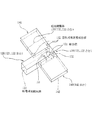
図1は本発明の一実施例を説明するための三方向から見た各部配置図(三面図)及び各部配置斜視図であり、(b)は放射導波管20の一方の広壁面と給電導波管10の一方の狭壁面が同一面となっている面を水平にしたときに上から見た上面平面図であり、給電導波管の内部が分かるようにS字曲線から右方の狭壁面を切り欠いた図、(a)は(b)を左方から見た側面図、(c)は(b)を下方から見た側面図である。(d)は(a)のものを下面側(紙面の向う側)の方から見上げた斜視図である。このような配置では給電導波管10の一方の狭壁面が上面となり、他方の狭壁面が底面11となる。図2は図1の(d)の斜視図と同様の図に管内での反射を矢印点線で示した図である。
この実施例は、給電導波管10の両サイドに複数本づつの放射導波管20がその一端をこの給電導波管10と接続して配置され、給電導波管10の底面11には、各放射導波管20との接続部位に対応させて、反射抑圧壁30が配置されていて、これら反射抑圧壁により、給電導波管10からの電力をこれら放射導波管20へと給電する装置における、中央給電導波管終端電力分配器であって、給電導波管10の終端部分に近接して接続された放射導波管20に対し電力を給電する反射抑圧壁30は、給電導波管10の終端面12からの反射波及び終端部分の放射導波管20からの反射波を抑圧する位置及び高さで配置されている。このような反射波を抑圧するために、終端部分の反射抑圧壁30の配置位置(図1における寸法L)を、終端面12から導波管管内波長のほぼ1/4波長分離れた位置としている。
Next, embodiments of the present invention will be described with reference to the drawings.
FIG. 1 is a layout view of each part (three-sided view) and a perspective view of each part layout viewed from three directions for explaining an embodiment of the present invention, and FIG. FIG. 5 is a top plan view seen from above when a plane in which one narrow wall surface of the
In this embodiment, a plurality of
また、給電導波管10の終端部分に近接して接続された放射導波管20と、給電導波管10との接続部分である結合窓40は、給電導波管10と放射導波管20との結合を最大にするために、背景技術の第2の例(図6)におけるような結合調整部130は無く、放射導波管20自身の横断面開口がそれのみで直接給電導波管10と結合した構造となっている。
更に、給電導波管10の終端面12には、そのコーナー部分に、ザグリ加工やダイキャストによるコーナー丸み50がついている。なお、コーナー丸みがついていない場合でも動作する。
In addition, the
Further, the
以上のように、終端部分に最も近い反射抑圧壁30を、給電導波管10の終端面12からほぼ1/4波長離れた位置に配置し、かつその高さを調整すると、終端面12からの反射波aは給電源側からの波に対し逆相となるので互いに逆相となって打ち消し合って抑圧され、反射波が給電源側に戻ることはないか少なくなる。なお、放射導波管20からの反射波bは反射抑圧壁30で反射して給電導波管10の終端面12で反射するので、同様に打ち消すことができる。従って、各放射導波管20に対し、給電導波管10からの電力を十分給電することができるようになる。
As described above, when the
この実施例では終端部分の反射抑圧壁の位置をL=1/4・λとしているので、給電導波管10の終端面12部分が、放射導波管20の外側の狭壁面より突出した構造となっている。
なお、給電導波管10及び放射導波管20を含む、背景技術の第2の例におけるアンテナベース部100に相当する部分は、ザグリ加工等により、一層構造にて製作することができる。
In this embodiment, since the position of the reflection suppression wall at the end portion is L = 1/4 · λ, the
The portion corresponding to the
10 給電導波管
11 底面
12 終端面
20 放射導波管
30 反射抑圧壁
40 結合窓
50 コーナー丸み
100,100y アンテナベース部
110,110y 給電源導波孔
120,120y 給電導波路
121 反射抑圧壁
122,123 給電導波路底面
124,125 誘電性ポスト
130 結合調整部
140,140y 放射導波路
DESCRIPTION OF
Claims (3)
Priority Applications (1)
| Application Number | Priority Date | Filing Date | Title |
|---|---|---|---|
| JP2005042053A JP4573352B2 (en) | 2005-02-18 | 2005-02-18 | Center-fed waveguide terminated power divider |
Applications Claiming Priority (1)
| Application Number | Priority Date | Filing Date | Title |
|---|---|---|---|
| JP2005042053A JP4573352B2 (en) | 2005-02-18 | 2005-02-18 | Center-fed waveguide terminated power divider |
Publications (2)
| Publication Number | Publication Date |
|---|---|
| JP2006229679A JP2006229679A (en) | 2006-08-31 |
| JP4573352B2 true JP4573352B2 (en) | 2010-11-04 |
Family
ID=36990612
Family Applications (1)
| Application Number | Title | Priority Date | Filing Date |
|---|---|---|---|
| JP2005042053A Active JP4573352B2 (en) | 2005-02-18 | 2005-02-18 | Center-fed waveguide terminated power divider |
Country Status (1)
| Country | Link |
|---|---|
| JP (1) | JP4573352B2 (en) |
Families Citing this family (4)
| Publication number | Priority date | Publication date | Assignee | Title |
|---|---|---|---|---|
| JP4531033B2 (en) * | 2006-10-23 | 2010-08-25 | 日本無線株式会社 | Ridge waveguide center-fed slot array antenna |
| JP5780995B2 (en) * | 2012-03-27 | 2015-09-16 | 三菱電機株式会社 | Rectangular waveguide connection structure |
| CN106410347A (en) * | 2016-10-17 | 2017-02-15 | 中国电子科技集团公司第五十四研究所 | Novel 3dB waveguide power divider |
| KR102521923B1 (en) * | 2022-06-13 | 2023-04-17 | (주)이랑텍 | Device for Magic-T signal branching |
Citations (5)
| Publication number | Priority date | Publication date | Assignee | Title |
|---|---|---|---|---|
| GB678632A (en) * | 1950-04-04 | 1952-09-03 | British Thomson Houston Co Ltd | Improvements relating to wave guides |
| JPH0427605U (en) * | 1990-06-28 | 1992-03-05 | ||
| JPH0548309A (en) * | 1991-08-09 | 1993-02-26 | Matsushita Electric Works Ltd | Waveguide branch circuit |
| JP2005167755A (en) * | 2003-12-04 | 2005-06-23 | Japan Radio Co Ltd | Waveguide slot array antenna |
| JP4373868B2 (en) * | 2004-07-21 | 2009-11-25 | 日本無線株式会社 | Center-fed waveguide planar slot antenna |
-
2005
- 2005-02-18 JP JP2005042053A patent/JP4573352B2/en active Active
Patent Citations (5)
| Publication number | Priority date | Publication date | Assignee | Title |
|---|---|---|---|---|
| GB678632A (en) * | 1950-04-04 | 1952-09-03 | British Thomson Houston Co Ltd | Improvements relating to wave guides |
| JPH0427605U (en) * | 1990-06-28 | 1992-03-05 | ||
| JPH0548309A (en) * | 1991-08-09 | 1993-02-26 | Matsushita Electric Works Ltd | Waveguide branch circuit |
| JP2005167755A (en) * | 2003-12-04 | 2005-06-23 | Japan Radio Co Ltd | Waveguide slot array antenna |
| JP4373868B2 (en) * | 2004-07-21 | 2009-11-25 | 日本無線株式会社 | Center-fed waveguide planar slot antenna |
Also Published As
| Publication number | Publication date |
|---|---|
| JP2006229679A (en) | 2006-08-31 |
Similar Documents
| Publication | Publication Date | Title |
|---|---|---|
| US8134514B2 (en) | Coaxial line slot array antenna and method for manufacturing the same | |
| JP5925243B2 (en) | Broadband microstrip antenna and antenna array | |
| KR102505800B1 (en) | Wireless communication device with leaky wave phased array antenna | |
| WO2019213878A1 (en) | Millimeter wave antenna array unit, array antenna, and communication product | |
| JP6386182B2 (en) | Waveguide slot array antenna | |
| US20090121952A1 (en) | Slot Antenna | |
| JP4727568B2 (en) | Waveguide array antenna | |
| JP4888143B2 (en) | T-branch waveguide and array antenna | |
| CN106340711B (en) | Dual-polarized antenna | |
| US20090160730A1 (en) | Dual polarised radiating element for cellular base station antennas | |
| JP4773226B2 (en) | antenna | |
| JP4612559B2 (en) | Waveguide slot array antenna | |
| US8704718B2 (en) | Waveguide to dipole radiator transition for rotating the polarization orthogonally | |
| JP4573352B2 (en) | Center-fed waveguide terminated power divider | |
| KR102402292B1 (en) | Dual polarization horn antenna | |
| JP5424954B2 (en) | Waveguide slot array antenna | |
| CN111106443B (en) | Single-unit beam forming dielectric resonant antenna | |
| JP6720796B2 (en) | Antenna and radar | |
| WO2020020054A1 (en) | Terminal device | |
| US10741924B1 (en) | Hybrid notch antenna | |
| EP1139489A1 (en) | Primary radiator having improved receiving efficiency by reducing side lobes | |
| WO2021021017A1 (en) | A dipole antenna, an antenna array, and a method of fabricating the dipole antenna and the antenna array | |
| JP3321589B2 (en) | Primary radiator for satellite receiving antenna and converter for satellite receiving | |
| JP4178265B2 (en) | Waveguide horn antenna, antenna device, and radar device | |
| JP5633097B2 (en) | Stacked two-dimensional slot array antenna |
Legal Events
| Date | Code | Title | Description |
|---|---|---|---|
| A621 | Written request for application examination |
Free format text: JAPANESE INTERMEDIATE CODE: A621 Effective date: 20080117 |
|
| A977 | Report on retrieval |
Free format text: JAPANESE INTERMEDIATE CODE: A971007 Effective date: 20090302 |
|
| A131 | Notification of reasons for refusal |
Free format text: JAPANESE INTERMEDIATE CODE: A131 Effective date: 20091104 |
|
| A521 | Written amendment |
Free format text: JAPANESE INTERMEDIATE CODE: A523 Effective date: 20091224 |
|
| A131 | Notification of reasons for refusal |
Free format text: JAPANESE INTERMEDIATE CODE: A131 Effective date: 20100121 |
|
| A521 | Written amendment |
Free format text: JAPANESE INTERMEDIATE CODE: A523 Effective date: 20100310 |
|
| A02 | Decision of refusal |
Free format text: JAPANESE INTERMEDIATE CODE: A02 Effective date: 20100330 |
|
| A521 | Written amendment |
Free format text: JAPANESE INTERMEDIATE CODE: A523 Effective date: 20100527 |
|
| A521 | Written amendment |
Free format text: JAPANESE INTERMEDIATE CODE: A821 Effective date: 20100527 |
|
| A911 | Transfer of reconsideration by examiner before appeal (zenchi) |
Free format text: JAPANESE INTERMEDIATE CODE: A911 Effective date: 20100707 |
|
| TRDD | Decision of grant or rejection written | ||
| A01 | Written decision to grant a patent or to grant a registration (utility model) |
Free format text: JAPANESE INTERMEDIATE CODE: A01 Effective date: 20100816 |
|
| A01 | Written decision to grant a patent or to grant a registration (utility model) |
Free format text: JAPANESE INTERMEDIATE CODE: A01 |
|
| A61 | First payment of annual fees (during grant procedure) |
Free format text: JAPANESE INTERMEDIATE CODE: A61 Effective date: 20100816 |
|
| R150 | Certificate of patent or registration of utility model |
Ref document number: 4573352 Country of ref document: JP Free format text: JAPANESE INTERMEDIATE CODE: R150 Free format text: JAPANESE INTERMEDIATE CODE: R150 |
|
| FPAY | Renewal fee payment (event date is renewal date of database) |
Free format text: PAYMENT UNTIL: 20130827 Year of fee payment: 3 |