JP4570867B2 - Photoelectric conversion element - Google Patents
Photoelectric conversion element Download PDFInfo
- Publication number
- JP4570867B2 JP4570867B2 JP2003430607A JP2003430607A JP4570867B2 JP 4570867 B2 JP4570867 B2 JP 4570867B2 JP 2003430607 A JP2003430607 A JP 2003430607A JP 2003430607 A JP2003430607 A JP 2003430607A JP 4570867 B2 JP4570867 B2 JP 4570867B2
- Authority
- JP
- Japan
- Prior art keywords
- working electrode
- electrode
- photoelectric conversion
- conversion element
- contact
- Prior art date
- Legal status (The legal status is an assumption and is not a legal conclusion. Google has not performed a legal analysis and makes no representation as to the accuracy of the status listed.)
- Expired - Fee Related
Links
Images
Classifications
-
- Y—GENERAL TAGGING OF NEW TECHNOLOGICAL DEVELOPMENTS; GENERAL TAGGING OF CROSS-SECTIONAL TECHNOLOGIES SPANNING OVER SEVERAL SECTIONS OF THE IPC; TECHNICAL SUBJECTS COVERED BY FORMER USPC CROSS-REFERENCE ART COLLECTIONS [XRACs] AND DIGESTS
- Y02—TECHNOLOGIES OR APPLICATIONS FOR MITIGATION OR ADAPTATION AGAINST CLIMATE CHANGE
- Y02E—REDUCTION OF GREENHOUSE GAS [GHG] EMISSIONS, RELATED TO ENERGY GENERATION, TRANSMISSION OR DISTRIBUTION
- Y02E10/00—Energy generation through renewable energy sources
- Y02E10/50—Photovoltaic [PV] energy
- Y02E10/542—Dye sensitized solar cells
-
- Y—GENERAL TAGGING OF NEW TECHNOLOGICAL DEVELOPMENTS; GENERAL TAGGING OF CROSS-SECTIONAL TECHNOLOGIES SPANNING OVER SEVERAL SECTIONS OF THE IPC; TECHNICAL SUBJECTS COVERED BY FORMER USPC CROSS-REFERENCE ART COLLECTIONS [XRACs] AND DIGESTS
- Y02—TECHNOLOGIES OR APPLICATIONS FOR MITIGATION OR ADAPTATION AGAINST CLIMATE CHANGE
- Y02P—CLIMATE CHANGE MITIGATION TECHNOLOGIES IN THE PRODUCTION OR PROCESSING OF GOODS
- Y02P70/00—Climate change mitigation technologies in the production process for final industrial or consumer products
- Y02P70/50—Manufacturing or production processes characterised by the final manufactured product
Landscapes
- Photovoltaic Devices (AREA)
- Hybrid Cells (AREA)
Description
本発明は、色素増感太陽電池などの光電変換素子に係る。より詳細には、電解質層を作用極と対極で挟んでなる積層体からなるセル自体に加熱などの負荷をかけることなく、セル構成部材とその外側に配されるパッケージ材とを一括で封止することが可能な、光電変換素子に関する。 The present invention relates to a photoelectric conversion element such as a dye-sensitized solar cell. More specifically, the cell component and the package material disposed outside the cell are sealed together without applying a load such as heating to the cell itself composed of a laminate formed by sandwiching the electrolyte layer between the working electrode and the counter electrode. What can be relates to a photoelectric conversion element.
環境問題、資源問題などを背景に、クリーンエネルギーとしての太陽電池が注目を集めている。太陽電池としては単結晶、多結晶あるいはアモルファスのシリコンを用いたものがある。しかし、従来のシリコン系太陽電池は製造コストが高い、原料供給が不充分などの課題が残されており、大幅普及には至っていない。
また、Cu−In−Se系(CIS系とも呼ぶ)などの化合物系太陽電池が開発されており、極めて高い変換効率を示すなど優れた特徴を有しているが、コストや環境負荷などの問題があり、やはり大幅普及への障害となっている。
Against the backdrop of environmental problems and resource problems, solar cells as clean energy are attracting attention. Some solar cells use single crystal, polycrystalline or amorphous silicon. However, conventional silicon-based solar cells still have problems such as high manufacturing costs and insufficient raw material supply, and have not yet been widely spread.
In addition, compound solar cells such as Cu-In-Se (also referred to as CIS) have been developed and have excellent features such as extremely high conversion efficiency, but problems such as cost and environmental impact It is still an obstacle to widespread use.
これらに対して、色素増感型太陽電池は、スイスのグレッツェルらのグループなどから提案されたもので、安価で高い変換効率を得られる光電変換素子として着目されている。
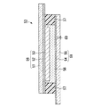
図3は、従来の色素増感型太陽電池の一例を示す模式的な断面図である。
この色素増感型太陽電池50は、増感色素を担持させた多孔質半導体電極(以下、色素増感半導体電極とも呼ぶ)53が一方の面に形成された第一基板51と、導電膜54が形成された第二基板55と、これらの間に封入された例えばゲル状電解質からなる電解質層56を主な構成要素としている。
On the other hand, the dye-sensitized solar cell has been proposed by a group such as Gretzel of Switzerland, and has attracted attention as a photoelectric conversion element that can be obtained at low cost and high conversion efficiency.
FIG. 3 is a schematic cross-sectional view showing an example of a conventional dye-sensitized solar cell.
The dye-sensitized
第一基板51としては光透過性の板材が用いられ、第一基板51の色素増感半導体電極53と接する面には導電性を持たせるために透明導電層52が配置されており、第一基板51、透明導電層52及び色素増感半導体電極53により窓極58をなす。
一方、第二基板55としては、電解質層56と接する側の面には導電性を持たせるために例えば炭素や白金からなる導電層54が設けられ、第二基板55及び導電層54により対極59を構成している。
A light-transmitting plate material is used as the
On the other hand, as the
色素増感半導体電極53と導電層54が対向するように、第一基板51と第二基板55を所定の間隔をおいて配置し、両基板間の周辺部に熱可塑性樹脂からなる封止剤57を設ける。そして、この封止剤57を介して2つの基板51、55を貼り合わせてセルを組み上げ、電解液の注入口60を通して、両極58、59間にヨウ素・ヨウ化物イオンなどの酸化・還元種を含む有機電解液を充填し、電荷移送用の電解質層56を形成したものが挙げられる。つまり、封止剤57は電解質層56中に含まれる電解液が漏出したり、揮発性成分が揮発したりするのを防ぐ役目を果たしている。この電解液の注入としては、太陽電池のセルを組み上げた上で、背面などに設けた注液口から毛細管現象、圧力差などを利用してバッチ式で注入している。
The
しかしながら、上述した従来の色素増感型太陽電池は、熱可塑性樹脂を用いて封止することにより封止剤57を形成していた。図3に示すように、具体的には、熱をかけて樹脂を溶融させ2枚の電極(窓極58、対極59)を接着していた。その際に、熱が第一基板51を介して色素増感半導体電極53まで達するため、色素増感半導体電極53に吸着した色素に悪影響を及ぼす恐れがあった。
また、封止剤57は樹脂で形成されているので、長期使用した際に耐候性の点において問題があった。
さらには、電解液を注入する際には、まず、2枚の電極板を融着しセルの形を組んでから、予め開けておいた注入口50を通して、極めて狭い空間をなす2枚の電極間に注入し、最後に注入口50に蓋をしなければならず、製造工程が複雑になる問題があった。また、電解液の粘度が高いと、電解液を注入するために多大な時間と手間を要することから、製造コストの増大をまねいていた。
However, the conventional dye-sensitized solar cell described above forms the
Moreover, since the
Furthermore, when injecting the electrolytic solution, first, two electrode plates are fused to form a cell shape, and then two electrodes forming an extremely narrow space through an
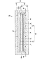
そこで、本発明者らは、電極を接着する際に加わる熱が色素増感半導体電極に吸着した色素に及ぼす影響を抑制するとともに、長期使用時における耐候性に優れ、かつ、電解液の注入を容易に行うことが可能な光電変換素子として、図4に示すような構成の光電変換素子70を開発した。光電変換素子70においては、2枚の電極(窓極(作用極)78、対極79)間は融着する形で封止するのではなく、箱体82と蓋体85からなる筐体81内に、電解質層76を作用極78と対極79で挟んでなる積層体80を収納し、箱体82と蓋体85を封止することで、セルをなす積層体80も含めて一括で封止することができる。
Therefore, the present inventors have suppressed the influence of the heat applied when bonding the electrodes to the dye adsorbed on the dye-sensitized semiconductor electrode, are excellent in weather resistance during long-term use, and are injected with an electrolyte. As a photoelectric conversion element that can be easily performed, a
図4の構成によれば、2枚の電極すなわち作用極78と対極79に熱が直接的に加わることがないので、上述した色素に対する熱の影響を回避できる。また、色素増感半導体電極73に電解液を滴下して挟み込むことにより、作用極78と対極79で挟んでなる積層体80を形成することが可能なため、電解液の注入工程が省けるという利点がある。さらに、作用極78と対極79は筐体81の内側に収納されているので、外部から直接的な衝撃を受けることがないため、外力に対する強度が確保されるという長所も備えている。
According to the configuration of FIG. 4, since heat is not directly applied to the two electrodes, that is, the working
しかしながら、光電変換素子70においては、封止する際に積層体80には上下方向(図4に示した矢印の方向)から第一基板71を介して圧力が加わることになるが、積層体80の側方には空隙80sや弾性部材86aが配されるため、積層体80の存在する領域に接する第一基板71の中央部にはほぼ面内均一に圧力が加わるが、空隙80sや弾性部材86aと接する位置にある第一基板71の端部には中央部とは異なる状態で圧力が加わることとなり、第一基板71が歪んだり破損する恐れがあった。この問題は、第一基板71に薄板を採用し光電変換素子70全体の薄型化を図る上で大きな障害となっていた。また、作用極78に一端が接続された導電体88は最短経路とするために弾性部材86aの中を通過するように配されていたが、弾性部材86aが変形したとき導電体88と作用極78との電気的な接続に不具合が生じる恐れがあった。
本発明は上記事情に鑑みてなされたもので、電極を構成する基板に歪みや破損が生じることなく封止でき、基板の薄型化も図れ、かつ、電気的な接続安定性も確保される、光電変換素子及びその製造方法を提供することを目的とする。 The present invention has been made in view of the above circumstances, and can be sealed without causing distortion or breakage in the substrate constituting the electrode, the substrate can be thinned, and electrical connection stability is ensured. It is an object of the present invention to provide a photoelectric conversion element and a manufacturing method thereof.
本発明に係る光電変換素子は、増感色素を表面に担持させた多孔質酸化物半導体層を有する作用極、該作用極の多孔質酸化物半導体層側においてこれに対向して配置される対極、及びこれら両極の間の少なくとも一部に電解質層を配した光電変換素子であって、
前記電解質層を作用極と対極で挟んでなる積層体は筐体内に収納され、前記積層体の上下面は前記筐体の内面と直接的または間接的に接しており、前記筐体のうち少なくとも作用極と接する部分は太陽光を透過する光学特性を備えた部材からなり、
前記筐体の内部を通過し前記積層体の側面に接触しないように、前記対極と前記作用極に一端がそれぞれ接続され、前記筐体の外に他端がそれぞれ延びる導電体を個別に設け、
前記作用極に一端が接続された導電体は、前記積層体の一側面と前記筐体との間に配された弾性部材と、前記筐体との接触面に沿って延びるように配置されていることを特徴としている。
The photoelectric conversion device according to the present invention includes a working electrode having a porous oxide semiconductor layer having a sensitizing dye supported on the surface thereof, and a counter electrode disposed opposite to the working electrode on the porous oxide semiconductor layer side. , And a photoelectric conversion element in which an electrolyte layer is disposed on at least a part between these two electrodes,
A laminate comprising the electrolyte layer sandwiched between a working electrode and a counter electrode is housed in a housing, and the upper and lower surfaces of the laminate are in direct or indirect contact with the inner surface of the housing, and at least of the housings. The part in contact with the working electrode consists of a member with optical properties that transmit sunlight,
One end is connected to each of the counter electrode and the working electrode so as not to pass through the inside of the case and contact the side surface of the stacked body, and separately provided conductors each extending the other end outside the case,
The conductor having one end connected to the working electrode is disposed so as to extend along a contact surface between the casing and the elastic member disposed between one side surface of the multilayer body and the casing. It is characterized by being.
上記光電変換素子では、電解質層を作用極と対極で挟んでなる積層体が、その上下面を筐体の内面と直接的または間接的に接するように収納されている。つまり、筐体の内面が積層体の上下面を挟み込むように構成したことにより、筐体を封止することで積層体からなるセル構成部材も含め一括で封止することが可能となるので、積層体に熱が加わる影響を著しく低減できる。ゆえに、電極接着時に加わる熱の影響を受けて色素が所定の機能を阻害されるという従来の課題は解消され、色素はその性能を安定に発揮できるので、光電変換特性の安定化が図れる。また、筐体のうち少なくとも作用極と接する部分が、太陽光を透過する光学特性を備えた部材から構成されていれば、太陽光を積層体からなるセル構成部材内に取り込むことができる。 In the above photoelectric conversion element, a laminate in which an electrolyte layer is sandwiched between a working electrode and a counter electrode is stored so that the upper and lower surfaces thereof are in direct or indirect contact with the inner surface of the housing. In other words, since the inner surface of the casing is configured to sandwich the upper and lower surfaces of the laminate, it is possible to seal the casing in a lump including the cell constituent members made of the laminate by sealing the casing. The influence of heat applied to the laminate can be significantly reduced. Therefore, the conventional problem that the dye is impeded by a predetermined function under the influence of heat applied at the time of electrode adhesion is solved, and the dye can exhibit its performance stably, so that the photoelectric conversion characteristics can be stabilized. Further, if at least a portion of the housing that is in contact with the working electrode is formed of a member having an optical characteristic that transmits sunlight, the sunlight can be taken into the cell constituent member formed of the laminate.
かかる構成の光電変換素子では、筐体の内部を通過し積層体の側面に接触しないように、対極と作用極に一端がそれぞれ接続され、筐体の外に他端がそれぞれ延びる導電体を個別に設けたことにより、光電変換素子は外部との電気的な接続が図れる。特に、作用極に一端が接続された導電体は、積層体の一側面と筐体との間に配された弾性部材と、前記筐体との接触面に沿って延びるように配置されているので、導電体が積層体の側面との接触して短絡するのを防止できるとともに、封止した際に弾性部材が変形しても導電体はその影響を受けることが無いので、導電体の一端と作用極との間で電気的接続の安定性が確保される。 In the photoelectric conversion element having such a configuration, one end is connected to each of the counter electrode and the working electrode and the other end is extended to the outside of the casing so as not to contact the side surface of the multilayer body through the inside of the casing. Thus, the photoelectric conversion element can be electrically connected to the outside. In particular, the conductor having one end connected to the working electrode is disposed so as to extend along the contact surface between the elastic member disposed between one side surface of the multilayer body and the housing and the housing. Therefore, the conductor can be prevented from coming into contact with the side surface of the laminated body and short-circuiting, and even if the elastic member is deformed when sealed, the conductor is not affected by this. And the stability of the electrical connection between the working electrode and the working electrode.
また、この構成を採用した光電変換素子では、電解質層を作用極と対極で挟んでなる積層体を利用できるので、例えば一方の電極上に液状の電解液を滴下(充填)して、その上から他方の電極を挟み込むことで積層体を形成できる。その際、電極間に挟まれた電解液は、毛細管現象により隙間からこぼれ出ることはない。また、ゲル状の電解質を挟み込んで充填することも可能である。したがって、従来多大な時間を要した電解液の注入工程を省けるので、光電変換素子の低コスト化を一段と図ることが可能となる。 In addition, in the photoelectric conversion element adopting this configuration, a laminate in which an electrolyte layer is sandwiched between a working electrode and a counter electrode can be used. For example, a liquid electrolyte solution is dropped (filled) on one electrode, A stacked body can be formed by sandwiching the other electrode. At that time, the electrolytic solution sandwiched between the electrodes does not spill out of the gap due to the capillary phenomenon. It is also possible to sandwich and fill the gel electrolyte. Therefore, it is possible to omit the electrolytic solution injection process which has conventionally required a lot of time, and thus it is possible to further reduce the cost of the photoelectric conversion element.
さらに、上記構成によれば、従来のように樹脂からなる封止剤を用いる必要がないため、長期使用時における耐候性が改善されることから、光電変換特性の長期安定性に優れた光電変換素子の提供が可能となる。
さらにまた、上記光電変換素子では、積層体からなるセル構成部材が筐体内に設置されており外気と触れることがない構成を採用している。すなわち、密閉された空間内にセル構成部材が納められているので、従来より対環境特性に優れた光電変換素子が得られる。
Furthermore, according to the above configuration, since it is not necessary to use a sealing agent made of resin as in the prior art, the weather resistance at the time of long-term use is improved, so that the photoelectric conversion excellent in the long-term stability of the photoelectric conversion characteristics An element can be provided.
Furthermore, in the said photoelectric conversion element, the cell structural member which consists of a laminated body is installed in the housing | casing, and the structure which does not touch external air is employ | adopted. That is, since the cell constituent member is housed in a sealed space, a photoelectric conversion element having better environmental characteristics than before can be obtained.
上述した光電変換素子において、筐体が積層体の側面と接するように配置することが好ましい。積層体の側方に空隙および/または弾性部材を設けないことにより、作用極はその中央部のみならず端部近傍においても必ず積層体と接した状態が保たれる。よって、封止時に、作用極は端部近傍で偏った圧力を受けることがないので、作用極を構成する基板などが歪んだり破損するという問題が解消される。
筐体が積層体の全ての側面と接するように配置する形態が最も好ましいが、作用極に一端が接続された導電体を積層体の厚さ方向へ導く箇所のみ、筐体と積層体との間に弾性部材を配置する形態としても構わない。後者の形態を採用した場合でも、前者の形態と同じ作用がほぼ同様に得られる。
In the above-described photoelectric conversion element, the housing is preferably disposed so as to be in contact with the side surface of the stacked body. By not providing a gap and / or an elastic member on the side of the laminated body, the working electrode is always kept in contact with the laminated body not only in the center but also in the vicinity of the end. Therefore, since the working electrode does not receive a biased pressure in the vicinity of the end portion during sealing, the problem that the substrate constituting the working electrode is distorted or damaged is solved.
A configuration in which the housing is arranged so as to be in contact with all the side surfaces of the laminated body is most preferable, but only the portion where the conductor having one end connected to the working electrode is guided in the thickness direction of the laminated body is provided between the housing and the laminated body. A configuration may be adopted in which an elastic member is disposed therebetween. Even when the latter form is adopted, the same action as that of the former form can be obtained almost similarly.
このように作用極がその端部近傍で偏った圧力を受けにくい形態とすることにより、作用極を構成する(第一)基板の厚さを、0.1mm以上0.5mm以下の範囲に薄く設定することが可能となる。0.1mm未満とした場合は、基板自体の機械的強度が低下し、製造において基板をハンドリングする際や、筐体に収納し封止するため圧力を加えた際に、基板が変形したり損壊する恐れがあるので芳しくない。0.5mmを越える場合は、基板に歪みや反りが発生しやすくなり、筐体を構成する蓋体から不均一に圧力が加わることもあり、作用極と対極との電極間距離が不均一な状態となるので、発電特性の安定性を低下させる。したがって、作用極を構成する(第一)基板の厚さは、0.1mm以上0.5mm以下の範囲が好適であり、このような薄い基板の採用は、光電変換素子の薄型化をもたらすので好ましい。 In this way, by making the working electrode less susceptible to biased pressure in the vicinity of its end, the thickness of the (first) substrate constituting the working electrode is reduced to a range of 0.1 mm to 0.5 mm. It becomes possible to set. If the thickness is less than 0.1 mm, the mechanical strength of the substrate itself is reduced, and the substrate may be deformed or damaged when the substrate is handled in manufacturing or when pressure is applied to store and seal the housing. It is not good because there is a risk of doing. When the thickness exceeds 0.5 mm, the substrate is likely to be distorted or warped, and pressure may be applied nonuniformly from the lid constituting the housing, and the distance between the working electrode and the counter electrode is not uniform. Therefore, the stability of the power generation characteristics is reduced. Therefore, the thickness of the (first) substrate constituting the working electrode is preferably in the range of 0.1 mm or more and 0.5 mm or less, and the adoption of such a thin substrate results in a thinner photoelectric conversion element. preferable.
以下、実施の形態に基づいて本発明を説明するが、本発明は上述した作用と効果を満たす構成であればよく、これらの実施形態に限定されるものではない。 Hereinafter, the present invention will be described based on the embodiments. However, the present invention is not limited to these embodiments as long as the above-described functions and effects are satisfied.
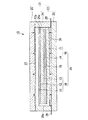
図1は、本発明に係る光電変換素子の一例を示す模式的な断面図である。
この色素増感型太陽電池(光電変換素子)10は、増感色素を表面に担持させた多孔質酸化物半導体層(酸化物電極とも呼ぶ)13を有する作用極(窓極とも呼ぶ)18と、作用極18の多孔質酸化物半導体層13側においてこれに対向して配置される対極19と、及びこれら両極の間の少なくとも一部に電解質層16とを配してなる。作用極18は、例えば第一基板11とその上に順に配される透明導電膜12および酸化物電極13からなる。一方の対極19は、例えば第二基板15とその上に配される導電膜14からなる。
FIG. 1 is a schematic cross-sectional view showing an example of a photoelectric conversion element according to the present invention.
The dye-sensitized solar cell (photoelectric conversion element) 10 includes a working electrode (also referred to as a window electrode) 18 having a porous oxide semiconductor layer (also referred to as an oxide electrode) 13 having a sensitizing dye supported on a surface thereof. The
電解質層16を作用極18と対極19で挟んでなる積層体20がセル構成部材、すなわち光電変換素子として機能する。色素増感型太陽電池10において、積層体20はこれを取り囲む筐体21の内側に収納されており、積層体20の上下面は筐体21の内面と接している。ここで、筐体21のうち少なくとも作用極18と接する部分、すなわち図1に示した蓋体25は、太陽光を透過する光学特性を備えた部材から構成される。
A laminate 20 in which the
色素増感型太陽電池10では、電解質層16を作用極18と対極19で挟んでなる積層体20が、その上下面を筐体21の内面に接するように収納されており、筐体21の内面が積層体20の上下面を挟み込むような構成を備えている。したがって、筐体21を例えば蓋体25と箱体22の側部24が接する部分で封止すれば、積層体20からなるセル構成部材も含め一括で封止することが可能となる。
In the dye-sensitized
なお、図1において積層体20に向かう矢印は、筐体21を封止した際に積層体20に加わる力の方向を示している。積層体20に対してこのような向きに外力が加わったとき、積層体20において横ズレが発生するのを抑制したり、あるいは積層体20が上下方向に柔軟性を保ちながら強固に固定されるように積層体20を封止する目的から、対極19と筐体21を構成する底部23との間には弾性部材26を設けることが好ましい。
In addition, the arrow which goes to the
また、同様の理由から、作用極18と筐体を構成する蓋体25との間には隙間充填材27が挿入される。ただし、隙間充填材27は作用極18上に配置されることから明らかなように、隙間充填材27としては太陽光の透過特性に優れた材料が好適に用いられる。
弾性部材26や隙間充填材27の設置は、上下の電極がその面内方向に相対的な位置ずれを抑制するとともに、外力に対する高い形状安定や耐震性をもたらすので望ましい。
For the same reason, a
The installation of the
さらに、色素増感型太陽電池10では、筐体21の内部を通過し積層体20の側面に接触しないように、対極19と作用極18に一端がそれぞれ接続され、筐体21の外に他端がそれぞれ延びる導電体28,29を個別に設けてなる構成を採用している。
この構成によれば、不図示の外部回路と接続するために用いられる導電体28、29の他端を、筐体21の如何なる箇所からでも自由に筐体外に導出させることが可能なので、外部回路系に合わせた多様な設置条件に応えることができる。
Furthermore, in the dye-sensitized
According to this configuration, the other ends of the
作用極18に一端が接続され、筐体21の外に他端が延びる導電体28にあっては、筐体21の内部を通過し積層体20の側面に接触しないようにするため、例えば図1に示すように、積層体20の一部を構成する酸化物電極13、導電膜14および第二基板15の各側面と導電体28との間に弾性部材26aを挟む込むように設けても構わない。これにより、筐体の内部を通過し積層体の側面に接触しないように、対極と作用極に一端がそれぞれ接続され、筐体の外に他端がそれぞれ延びる導電体を個別に設けることが可能となり、光電変換素子は外部との電気的な接続が図れる。
In the
特に、光電変換素子10では、作用極18に一端が接続された導電体28は、積層体20の一側面と筐体21との間に設けられた弾性部材26aと、作用極12の端部12aとが接触してなる面に沿って延びるように配置されている。この配置は、導電体28が積層体20の側面と接触して短絡するのを防ぐ。また、封止した際に弾性部材26aが縮んでその形状が変化した場合でも、導電体28は弾性部材26aの中を通過せずに、作用極12の端部12aと弾性部材26aとの接触面に存在するので、その影響を大きく受けることは殆ど無い。よって、導電体28の一端と作用極18との電気的接続は極めて安定に保たれるので、この電気的接続の改善は光電変換素子の出力特性の長期安定性をもたらす。
In particular, in the
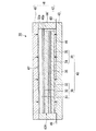
図2は、本発明に係る光電変換素子の他の一例を示す模式的な断面図である。図2に示す光電変換素子30は、筐体41が積層体40の側面40tと接するように配置した点が前述した実施形態(光電変換素子10)と異なる。このように積層体40の側方に空隙を設けない構成とすることにより、作用極38はその中央部のみならず端部近傍においても必ず積層体と接した状態が保たれる。すると、封止する際に、作用極38は端部近傍で偏った圧力を受けることがないので、作用極38を構成する第一基板31などが歪んだり破損する危険性を低く抑えることが可能となる。
FIG. 2 is a schematic cross-sectional view showing another example of the photoelectric conversion element according to the present invention. The
筐体が積層体の全ての側面と接するように配置する形態が最も好ましいが、図2に示すように、作用極38に一端が接続された導電体48を積層体38の厚さ方向へ導く箇所のみ、筐体41の側部44と光電変換素子10との間に弾性部材46aを配置する形態としても構わない。弾性部材46aとして絶縁性を有する部材を用いることにより、積層体40と導電体48が短絡する恐れが回避できるので好ましい。導電体48が存在する近傍のみに弾性部材46aを設けて、筐体41の他の側部と積層体40との間は接するように配置すれば、上述した作用がほぼ同様に得られる。
A configuration in which the housing is disposed so as to be in contact with all the side surfaces of the multilayer body is most preferable. However, as shown in FIG. 2, a
本発明に係る光電変換素子の製造方法は、増感色素を表面に担持させた多孔質酸化物半導体層を有する作用極、該作用極の多孔質酸化物半導体層側においてこれに対向して配置される対極、及びこれら両極の間の少なくとも一部に電解質層を配した光電変換素子の製造方法であって、
前記作用極を構成する多孔質酸化物半導体層に液状またはゲル状の電解質を充填して電解質層を形成する工程と、
筐体を構成する箱体の内底面に前記対極を設け、該対極に前記電解質層が接するように前記作用極を重ねて積層体を形成し、該作用極を覆うように前記筐体を構成する蓋体を配した後、前記筐体の外側から前記作用極を介して前記積層体の積層方向に荷重を加え、該荷重が前記作用極を構成する第一基板面に略均一に加わるようにして筐体を封止する工程と、
を少なくとも具備することを特徴としている。
The method for producing a photoelectric conversion device according to the present invention includes a working electrode having a porous oxide semiconductor layer having a sensitizing dye supported on the surface thereof, and is disposed opposite to the working electrode on the porous oxide semiconductor layer side. A counter electrode, and a method for producing a photoelectric conversion element in which an electrolyte layer is disposed at least in part between the two electrodes,
Filling the porous oxide semiconductor layer constituting the working electrode with a liquid or gel electrolyte to form an electrolyte layer; and
The counter electrode is provided on the inner bottom surface of the box constituting the housing, the working electrode is stacked so that the electrolyte layer is in contact with the counter electrode, a laminate is formed, and the housing is configured to cover the working electrode A load is applied in the stacking direction of the stacked body from the outside of the housing via the working electrode, and the load is applied substantially uniformly to the first substrate surface constituting the working electrode. Sealing the housing, and
It is characterized by comprising at least.
かかる製造方法であれば、まず、前記作用極を構成する多孔質酸化物半導体層に液状またはゲル状の電解質を充填して電解質層を形成する工程により、多孔質酸化物半導体層の表面上に電解液を均一に塗布することができる。すなわち、この工程によれば、従来のように作用極と対極との間の狭い空間に注入口を通して電解液を強制的に注入する必要がないため、作用極と対極との間において電解液が行き渡らない領域が発生したり、あるいは電解液が局在してしまう等の不具合が解消される。この作用・効果は、電解質が液状のみならず、ゲル状であっても有効に働く。 In such a manufacturing method, first, the step of forming an electrolyte layer by filling the porous oxide semiconductor layer constituting the working electrode with a liquid or gel electrolyte is performed on the surface of the porous oxide semiconductor layer. The electrolytic solution can be applied uniformly. That is, according to this process, there is no need to forcibly inject the electrolytic solution through the inlet into the narrow space between the working electrode and the counter electrode as in the prior art. Problems such as the occurrence of a region that does not spread or the localized presence of the electrolyte are eliminated. This action / effect works effectively even if the electrolyte is not only liquid but also gel.
次いで、前記筐体を構成する箱体の内底面に前記対極を設け、該対極に前記電解質層が接するように前記作用極を重ねて積層体を形成し、該作用極を覆うように前記筐体を構成する蓋体を配した後、前記筐体の外側から前記作用極を介して前記積層体の積層方向に荷重を加え、該荷重が前記作用極を構成する第一基板面に略均一に加わるようにして筐体を封止する工程により、筐体を封止することで積層体からなるセル構成部材も含め一括で封止することが可能となる。筐体を封止する際に、筐体に局所的は熱を加えたとしても、積層体に熱が加わることは殆どない。ゆえに、この工程を採用すれば、従来の電極接着時に加わる熱の影響を受けて色素が所定の機能を阻害されるという問題が解消される。また、荷重が前記作用極を構成する第一基板面に略均一に加わるようにして筐体を封止するので、作用極を構成する基板などが歪んだり破損することも防止できる。 Next, the counter electrode is provided on the inner bottom surface of the box constituting the casing, the working electrode is stacked so that the electrolyte layer is in contact with the counter electrode, a laminate is formed, and the casing is covered so as to cover the working electrode. After the lid constituting the body is disposed, a load is applied from the outside of the housing through the working electrode in the stacking direction of the laminated body, and the load is substantially uniform on the first substrate surface constituting the working electrode. In the step of sealing the casing as it is added to the case, it is possible to seal the casing in a lump including the cell constituent member made of a laminate by sealing the casing. Even when heat is locally applied to the housing when the housing is sealed, the laminate is hardly heated. Therefore, if this process is adopted, the problem that the dye is impeded by a predetermined function under the influence of heat applied during the conventional electrode bonding is solved. Further, since the casing is sealed so that the load is applied substantially uniformly to the first substrate surface constituting the working electrode, it is possible to prevent the substrate constituting the working electrode from being distorted or damaged.
したがって、本発明に係る製造方法は、上述した特徴を備えてなる光電変換素子、すなわち、電極を接着する際に加わる熱が色素増感半導体電極に吸着した色素に及ぼす影響を抑制できるとともに、長期使用時における耐候性に優れ、かつ、電解液の注入を容易に行うことが可能な光電変換素子の安定した製造に寄与する。さらに、封止に伴う作用極で発生していた不具合も解消され、電気的な接続の安定性が向上することから、本発明の製造方法は長期信頼性に優れた光電変換素子をもたらす。 Therefore, the manufacturing method according to the present invention can suppress the influence exerted on the dye adsorbed on the dye-sensitized semiconductor electrode by the heat applied when adhering the photoelectric conversion element having the above-described features, that is, the electrode, and for a long time. This contributes to stable production of a photoelectric conversion element that has excellent weather resistance during use and can be easily injected with an electrolyte. Furthermore, since the problem that has occurred at the working electrode due to sealing is also eliminated and the stability of electrical connection is improved, the manufacturing method of the present invention provides a photoelectric conversion element with excellent long-term reliability.
以下では、前述した光電変換素子10を例として好適な各構成部材を説明するが、光電変換素子30においても同じ構成部材を利用できることは言うまでもない。
本発明に係る第一基板11としては、光透過性の素材からなる板が用いられ、ガラス、ポリエチレンテレフタレート、ポリエチレンナフタレート、ポリカーボネート、ポリエーテルスルホンなど、通常太陽電池の透明基板として用いられるものであればどのようなものも用いることができる。電解液への耐性などを考慮して適宜選択すればよいが、用途上、できるだけ光透過性の高い基板が好ましい。
In the following, each of the suitable constituent members will be described by taking the above-described
As the
第一基板11の色素増感半導体電極13側の面には金属、炭素、導電性金属酸化物層などからなる透明導電膜12を形成して導電性を与えておくことが好ましい。透明導電膜12として金属層や炭素層を形成する場合には透明性を著しく損ねない構造とすることが好ましく、導電性と透明性を損なわない薄膜を形成できるものという観点から金属の種類も適宜選択される。導電性金属酸化物としては、例えばITO、SnO2 、フッ素ドープのSnO2 などを用いることができる。
It is preferable to provide conductivity by forming a transparent
第一基板11に載置された透明導電層2の上にはさらに半導体多孔質膜に増感色素を担持させてなる色素増感半導体電極13が設けられる。第一基板11、透明導電層2及び色素増感半導体電極13により作用極(窓極)18が構成される。色素増感半導体電極13の半導体多孔質膜を形成する半導体としては特に限定はされず、通常、太陽電池用の多孔質半導体を形成するに用いられるものであればどのようなものも用いることができ、例えば、TiO2 、SnO2 、WO3 、ZnO、Nb2O5などを用いることができる。多孔質膜を形成する方法としては、例えばゾルゲル法からの膜形成、微粒子の泳動電着、発泡剤による多孔質化、ポリマービーズなどとの混合物塗布後の余剰成分の除去などの方法を例示できるが、これらに限定されるものではない。
On the transparent conductive layer 2 placed on the
増感色素としては、ビピリジン構造、ターピリジン構造などを配位子に含むルテニウム錯体、ポルフィリン、フタロシアニン等の含金属錯体をはじめ、エオシン、ローダミン、メロシアニンなどの有機色素なども使用することができ、用途、使用半導体に適した励起挙動をとるものを特に限定無く選ぶことができる。 As sensitizing dyes, ruthenium complexes containing bipyridine structure, terpyridine structure, etc. as ligands, metal-containing complexes such as porphyrin, phthalocyanine, and organic dyes such as eosin, rhodamine, merocyanine, etc. can be used. Those having an excitation behavior suitable for the semiconductor used can be selected without particular limitation.
第二基板15としては、特に光透過性をもつ必要はないことから金属板を用いることができるし、第一基板11と同様のものを用いても構わない。第二基板15の上には導電膜14を設けた電極が対極19として用いられる。導電膜14としては、例えば炭素や白金などの層を、蒸着、スパッタ、塩化白金酸塗布後に熱処理を行ったものが好適に用いられるが、電極として機能するものであれば特に限定されるものではない。
As the
上述した作用極18と対極19との間には電解質層16が設けられ、積層体20からなるセル構成部材をなす。後述するように、本発明に係る積層体20は、作用極18を構成する多孔質酸化物半導体層13に液状またはゲル状の電解質を充填して電解質層16を形成した後、対極19に電解質層16が接するように作用極18を重ねて積層体20を形成した後、積層体20の積層方向に荷重を加える方法によって形成される。
ゆえに、本発明の電解質層16としては、従来は注入口から狭い電極間隙に注入することが困難であった粘性の高い材料でも使用できることから、適当なゲル化剤を用いて電解液をゲル化(擬固体化)したもので、かつ高粘度のものでも利用できるが、従来から用いられている如何なる材料であっても構わない。
An
Therefore, as the
電解質層16を作用極18と対極19で挟んでなる積層体20は筐体21内に収納されており、積層体20の上下面は筐体21の内面と接している。筐体21のうち少なくとも作用極18と接する部分、すなわち蓋体25は太陽光を透過する光学特性を備えた部材から構成され、例えばアクリル、ポリカーボネート、ポリ塩化ビニル、ソーダガラスなど透明で剛性のある材質が挙げられる。筐体21の他の部分、すなわち底部23と側部24から構成される箱体22は、2つの電極から各々、筐体21の外部回路に延びる導電体28、29との絶縁性さえ確保されていれば、特にその材料は限定されない。
A laminate 20 in which the
筐体21を構成する箱体22の内底面に対極19を設け、対極19に電解質層16が接するように作用極18を重ねて積層体20を形成し、この作用極18を覆うように筐体22を構成する蓋体25を配した後、筐体21の外側から積層体20の積層方向に荷重を加えて筐体21を封止することにより、色素増感型太陽電池10は得られる。
A
筐体21の封止方法は、例えば筐体21の側部24と蓋体25の接触部に圧力や熱を加えることにより行われる。しかし、積層体20は筐体21内には収納されているが、筐体21の封止箇所から離れて位置するように配置されているので、この封止に伴う熱が積層体20に及ぶ恐れはない。例えばレーザにより封止を行えば、熱可塑性樹脂を使わない構成にすることが可能となる。
The
また、電解質層16を形成する電解液を、作用極(窓極)18に滴下(電解液が液状の場合)もしくは作用極(窓極)18に配置(電解液がゲル状の場合)した後、対極19と挟み合わせることで充填することができる。よって、従来のように対極19に孔を開け、電解液を注入し、孔をふさぐという複雑な工程を省くことができるので、製造工程の簡略化や労力の削減が図れることから、低コストな光電変換素子が得られる。さらには、作用極(窓極)18を構成する第一基板11と筐体21を構成する蓋体25との間に、隙間充填材27としてシリコーンオイルを充填すると、第一基板11と蓋体25間に存在する空気層を除去することができ、透明度が上昇することから望ましい。
In addition, after the electrolytic solution forming the
本発明によれば、電極を構成する基板に歪みや破損が生じることなく封止でき、基板の薄型化も図れ、かつ、電気的な接続安定性も確保される、光電変換素子及びその製造方法を提供することができる。ゆえに、本発明は、電気的接続において高い信頼性を備え、出力特性の長期安定性を備えた光電変換素子の製造に貢献する。 ADVANTAGE OF THE INVENTION According to this invention, the photoelectric conversion element which can be sealed without generating distortion and a damage | wound in the board | substrate which comprises an electrode, can achieve thickness reduction of a board | substrate, and electrical connection stability is ensured, and its manufacturing method Can be provided. Therefore, the present invention contributes to the manufacture of a photoelectric conversion element having high reliability in electrical connection and long-term stability of output characteristics.
10、30 色素増感型太陽電池(光電変換素子)、11、31 第一基板、12、32 透明導電膜、13、33 多孔質酸化物半導体層(酸化物電極)、14、34 導電膜、15、35 第二基板、16、36 電解質層、18、38 作用極(窓極)、19、39 対極、20、40 積層体、21、41 筐体、22、42 箱体、23、43 底部、24、44 側部、25、45 蓋体(作用極と接する部分)、26、26a、46、46a 弾性部材、27、47 隙間充填材、28、29、48、49 導電体。
10, 30 Dye-sensitized solar cell (photoelectric conversion element), 11, 31 First substrate, 12, 32 Transparent conductive film, 13, 33 Porous oxide semiconductor layer (oxide electrode), 14, 34 Conductive film, 15, 35 Second substrate, 16, 36 Electrolyte layer, 18, 38 Working electrode (window electrode), 19, 39 Counter electrode, 20, 40 Laminate, 21, 41 Housing, 22, 42 Box, 23, 43
Claims (3)
前記電解質層を作用極と対極で挟んでなる積層体は筐体内に収納され、前記積層体の上下面は前記筐体の内面と直接的または間接的に接しており、前記筐体のうち少なくとも作用極と接する部分は太陽光を透過する光学特性を備えた部材からなり、
前記筐体の内部を通過し前記積層体の側面に接触しないように、前記対極と前記作用極に一端がそれぞれ接続され、前記筐体の外に他端がそれぞれ延びる導電体を個別に設け、
前記作用極に一端が接続された導電体は、前記積層体の一側面と前記筐体との間に配された弾性部材と、前記筐体との接触面に沿って延びるように配置されていることを特徴とする光電変換素子。 A working electrode having a porous oxide semiconductor layer carrying a sensitizing dye on its surface, a counter electrode disposed opposite to the working electrode on the porous oxide semiconductor layer side of the working electrode, and at least one of the two electrodes A photoelectric conversion element in which an electrolyte layer is arranged in a part,
A laminate comprising the electrolyte layer sandwiched between a working electrode and a counter electrode is housed in a housing, and the upper and lower surfaces of the laminate are in direct or indirect contact with the inner surface of the housing, and at least of the housings. The part in contact with the working electrode consists of a member with optical properties that transmit sunlight,
One end is connected to each of the counter electrode and the working electrode so as not to pass through the inside of the case and contact the side surface of the stacked body, and separately provided conductors each extending the other end outside the case,
The conductor having one end connected to the working electrode is disposed so as to extend along a contact surface between the casing and the elastic member disposed between one side surface of the multilayer body and the casing. A photoelectric conversion element characterized by comprising:
Priority Applications (1)
| Application Number | Priority Date | Filing Date | Title |
|---|---|---|---|
| JP2003430607A JP4570867B2 (en) | 2003-12-25 | 2003-12-25 | Photoelectric conversion element |
Applications Claiming Priority (1)
| Application Number | Priority Date | Filing Date | Title |
|---|---|---|---|
| JP2003430607A JP4570867B2 (en) | 2003-12-25 | 2003-12-25 | Photoelectric conversion element |
Publications (2)
| Publication Number | Publication Date |
|---|---|
| JP2005190817A JP2005190817A (en) | 2005-07-14 |
| JP4570867B2 true JP4570867B2 (en) | 2010-10-27 |
Family
ID=34788926
Family Applications (1)
| Application Number | Title | Priority Date | Filing Date |
|---|---|---|---|
| JP2003430607A Expired - Fee Related JP4570867B2 (en) | 2003-12-25 | 2003-12-25 | Photoelectric conversion element |
Country Status (1)
| Country | Link |
|---|---|
| JP (1) | JP4570867B2 (en) |
Families Citing this family (3)
| Publication number | Priority date | Publication date | Assignee | Title |
|---|---|---|---|---|
| JP5192769B2 (en) * | 2007-10-12 | 2013-05-08 | 古河電気工業株式会社 | Dye-sensitized solar cell |
| JP2009146625A (en) * | 2007-12-12 | 2009-07-02 | Sony Corp | Dye-sensitized photoelectric conversion element module and manufacturing method thereof, photoelectric conversion element module and manufacturing method thereof, and electronic apparatus |
| WO2009144898A1 (en) * | 2008-05-27 | 2009-12-03 | 株式会社フジクラ | Photoelectric conversion element |
Family Cites Families (2)
| Publication number | Priority date | Publication date | Assignee | Title |
|---|---|---|---|---|
| JP4531388B2 (en) * | 2003-12-25 | 2010-08-25 | 株式会社フジクラ | Method for manufacturing photoelectric conversion element |
| JP4545429B2 (en) * | 2003-08-06 | 2010-09-15 | 株式会社フジクラ | Photoelectric conversion element and manufacturing method thereof |
-
2003
- 2003-12-25 JP JP2003430607A patent/JP4570867B2/en not_active Expired - Fee Related
Also Published As
| Publication number | Publication date |
|---|---|
| JP2005190817A (en) | 2005-07-14 |
Similar Documents
| Publication | Publication Date | Title |
|---|---|---|
| AU2004302117B2 (en) | Photoelectric converter and method for manufacturing same | |
| CN101842934B (en) | Dye-sensitized solar cell module | |
| CN102792518B (en) | Dye sensitization solar cell module and manufacture method thereof | |
| CN101601139A (en) | Dye-sensitized solar cell and preparation method thereof | |
| EP2346054A2 (en) | Photoelectric Conversion Module | |
| KR100384893B1 (en) | Nano-particle oxide solar cells and fabrication method of the same and solar cell modules and transparent electric window using the same | |
| JP5495447B2 (en) | Photoelectric conversion module and manufacturing method thereof | |
| JP4545429B2 (en) | Photoelectric conversion element and manufacturing method thereof | |
| JP2007042460A (en) | Dye-sensitized solar cell and sealing method thereof | |
| JP4570867B2 (en) | Photoelectric conversion element | |
| JP4531388B2 (en) | Method for manufacturing photoelectric conversion element | |
| JP2007048674A (en) | Dye-sensitized solar cell and sealing method thereof | |
| US20110220181A1 (en) | Photoelectric conversion module | |
| JP4606754B2 (en) | Photoelectric conversion element | |
| JP5362642B2 (en) | Dye-sensitized solar cell | |
| CN100536224C (en) | Photoelectric conversion element and method for manufacturing same | |
| EP2343717A2 (en) | Photoelectrochemical module | |
| JP2010199082A (en) | Photoelectric conversion element | |
| JP4689183B2 (en) | Dye-sensitized solar cell | |
| JP2009016174A (en) | Photoelectric conversion element | |
| TWI404216B (en) | Dye-sensitized solar cells | |
| US20120305054A1 (en) | Photoelectric conversion module | |
| US20110017396A1 (en) | Method of manufacturing photoelectric conversion element | |
| JP4606764B2 (en) | Photoelectric conversion element | |
| WO2009089562A1 (en) | Photovoltaic module |
Legal Events
| Date | Code | Title | Description |
|---|---|---|---|
| A621 | Written request for application examination |
Free format text: JAPANESE INTERMEDIATE CODE: A621 Effective date: 20060720 |
|
| A131 | Notification of reasons for refusal |
Free format text: JAPANESE INTERMEDIATE CODE: A131 Effective date: 20100316 |
|
| A521 | Request for written amendment filed |
Free format text: JAPANESE INTERMEDIATE CODE: A523 Effective date: 20100517 |
|
| TRDD | Decision of grant or rejection written | ||
| A01 | Written decision to grant a patent or to grant a registration (utility model) |
Free format text: JAPANESE INTERMEDIATE CODE: A01 Effective date: 20100803 |
|
| A01 | Written decision to grant a patent or to grant a registration (utility model) |
Free format text: JAPANESE INTERMEDIATE CODE: A01 |
|
| A61 | First payment of annual fees (during grant procedure) |
Free format text: JAPANESE INTERMEDIATE CODE: A61 Effective date: 20100811 |
|
| FPAY | Renewal fee payment (event date is renewal date of database) |
Free format text: PAYMENT UNTIL: 20130820 Year of fee payment: 3 |
|
| R151 | Written notification of patent or utility model registration |
Ref document number: 4570867 Country of ref document: JP Free format text: JAPANESE INTERMEDIATE CODE: R151 |
|
| FPAY | Renewal fee payment (event date is renewal date of database) |
Free format text: PAYMENT UNTIL: 20130820 Year of fee payment: 3 |
|
| R250 | Receipt of annual fees |
Free format text: JAPANESE INTERMEDIATE CODE: R250 |
|
| R250 | Receipt of annual fees |
Free format text: JAPANESE INTERMEDIATE CODE: R250 |
|
| R250 | Receipt of annual fees |
Free format text: JAPANESE INTERMEDIATE CODE: R250 |
|
| R250 | Receipt of annual fees |
Free format text: JAPANESE INTERMEDIATE CODE: R250 |
|
| R250 | Receipt of annual fees |
Free format text: JAPANESE INTERMEDIATE CODE: R250 |
|
| R250 | Receipt of annual fees |
Free format text: JAPANESE INTERMEDIATE CODE: R250 |
|
| R250 | Receipt of annual fees |
Free format text: JAPANESE INTERMEDIATE CODE: R250 |
|
| R250 | Receipt of annual fees |
Free format text: JAPANESE INTERMEDIATE CODE: R250 |
|
| R250 | Receipt of annual fees |
Free format text: JAPANESE INTERMEDIATE CODE: R250 |
|
| R250 | Receipt of annual fees |
Free format text: JAPANESE INTERMEDIATE CODE: R250 |
|
| LAPS | Cancellation because of no payment of annual fees |