JP4570848B2 - Organic photoreceptor, image forming method, image forming apparatus, and process cartridge - Google Patents
Organic photoreceptor, image forming method, image forming apparatus, and process cartridge Download PDFInfo
- Publication number
- JP4570848B2 JP4570848B2 JP2003135680A JP2003135680A JP4570848B2 JP 4570848 B2 JP4570848 B2 JP 4570848B2 JP 2003135680 A JP2003135680 A JP 2003135680A JP 2003135680 A JP2003135680 A JP 2003135680A JP 4570848 B2 JP4570848 B2 JP 4570848B2
- Authority
- JP
- Japan
- Prior art keywords
- toner
- image
- organic photoreceptor
- particles
- charge generation
- Prior art date
- Legal status (The legal status is an assumption and is not a legal conclusion. Google has not performed a legal analysis and makes no representation as to the accuracy of the status listed.)
- Expired - Fee Related
Links
- 238000000034 method Methods 0.000 title claims description 88
- 108091008695 photoreceptors Proteins 0.000 title claims description 88
- 230000008569 process Effects 0.000 title claims description 22
- 239000002245 particle Substances 0.000 claims description 244
- 239000000049 pigment Substances 0.000 claims description 96
- 239000000463 material Substances 0.000 claims description 53
- 238000012546 transfer Methods 0.000 claims description 45
- 238000009826 distribution Methods 0.000 claims description 40
- SJHHDDDGXWOYOE-UHFFFAOYSA-N oxytitamium phthalocyanine Chemical compound [Ti+2]=O.C12=CC=CC=C2C(N=C2[N-]C(C3=CC=CC=C32)=N2)=NC1=NC([C]1C=CC=CC1=1)=NC=1N=C1[C]3C=CC=CC3=C2[N-]1 SJHHDDDGXWOYOE-UHFFFAOYSA-N 0.000 claims description 25
- 238000004140 cleaning Methods 0.000 claims description 24
- 150000001875 compounds Chemical class 0.000 claims description 24
- 239000013078 crystal Substances 0.000 claims description 21
- 239000000126 substance Substances 0.000 claims description 18
- OWBTYPJTUOEWEK-UHFFFAOYSA-N (-)-(2R,3R)--2,3-butanediol Natural products CC(O)C(C)O OWBTYPJTUOEWEK-UHFFFAOYSA-N 0.000 claims description 14
- OWBTYPJTUOEWEK-QWWZWVQMSA-N (R,R)-butane-2,3-diol Chemical compound C[C@@H](O)[C@@H](C)O OWBTYPJTUOEWEK-QWWZWVQMSA-N 0.000 claims description 10
- OWBTYPJTUOEWEK-IMJSIDKUSA-N (S,S)-butane-2,3-diol Chemical compound C[C@H](O)[C@H](C)O OWBTYPJTUOEWEK-IMJSIDKUSA-N 0.000 claims description 6
- MZZSDCJQCLYLLL-UHFFFAOYSA-N Secalonsaeure A Natural products COC(=O)C12OC3C(CC1=C(O)CC(C)C2O)C(=CC=C3c4ccc(O)c5C(=O)C6=C(O)CC(C)C(O)C6(Oc45)C(=O)OC)O MZZSDCJQCLYLLL-UHFFFAOYSA-N 0.000 claims description 4
- 230000005525 hole transport Effects 0.000 claims description 2
- 239000010410 layer Substances 0.000 description 158
- 229920005989 resin Polymers 0.000 description 76
- 239000011347 resin Substances 0.000 description 76
- 238000003756 stirring Methods 0.000 description 49
- -1 perylene compound Chemical class 0.000 description 42
- 239000000243 solution Substances 0.000 description 35
- XLYOFNOQVPJJNP-UHFFFAOYSA-N water Substances O XLYOFNOQVPJJNP-UHFFFAOYSA-N 0.000 description 33
- 230000007547 defect Effects 0.000 description 27
- 239000007788 liquid Substances 0.000 description 26
- 239000000178 monomer Substances 0.000 description 25
- 238000006243 chemical reaction Methods 0.000 description 24
- 239000006185 dispersion Substances 0.000 description 24
- GWEVSGVZZGPLCZ-UHFFFAOYSA-N Titan oxide Chemical compound O=[Ti]=O GWEVSGVZZGPLCZ-UHFFFAOYSA-N 0.000 description 22
- OKKJLVBELUTLKV-UHFFFAOYSA-N Methanol Chemical compound OC OKKJLVBELUTLKV-UHFFFAOYSA-N 0.000 description 21
- VYPSYNLAJGMNEJ-UHFFFAOYSA-N Silicium dioxide Chemical compound O=[Si]=O VYPSYNLAJGMNEJ-UHFFFAOYSA-N 0.000 description 21
- 238000011156 evaluation Methods 0.000 description 20
- 238000004519 manufacturing process Methods 0.000 description 20
- 239000011230 binding agent Substances 0.000 description 18
- 239000003795 chemical substances by application Substances 0.000 description 18
- 238000000576 coating method Methods 0.000 description 18
- 239000003086 colorant Substances 0.000 description 18
- 238000006116 polymerization reaction Methods 0.000 description 18
- 239000007787 solid Substances 0.000 description 18
- 239000011248 coating agent Substances 0.000 description 17
- OGIDPMRJRNCKJF-UHFFFAOYSA-N titanium oxide Inorganic materials [Ti]=O OGIDPMRJRNCKJF-UHFFFAOYSA-N 0.000 description 17
- 241000519995 Stachys sylvatica Species 0.000 description 14
- 239000012736 aqueous medium Substances 0.000 description 14
- 239000010419 fine particle Substances 0.000 description 14
- 229910052751 metal Inorganic materials 0.000 description 14
- 239000002184 metal Substances 0.000 description 14
- 229920000642 polymer Polymers 0.000 description 14
- 230000035945 sensitivity Effects 0.000 description 14
- 238000011161 development Methods 0.000 description 12
- 238000010438 heat treatment Methods 0.000 description 12
- 238000004381 surface treatment Methods 0.000 description 12
- 238000011282 treatment Methods 0.000 description 12
- 230000000694 effects Effects 0.000 description 11
- 230000005684 electric field Effects 0.000 description 11
- YCKRFDGAMUMZLT-UHFFFAOYSA-N Fluorine atom Chemical compound [F] YCKRFDGAMUMZLT-UHFFFAOYSA-N 0.000 description 10
- 229910052731 fluorine Inorganic materials 0.000 description 10
- 239000011737 fluorine Substances 0.000 description 10
- 239000000203 mixture Substances 0.000 description 10
- 230000003287 optical effect Effects 0.000 description 10
- 239000002904 solvent Substances 0.000 description 10
- PPBRXRYQALVLMV-UHFFFAOYSA-N Styrene Chemical compound C=CC1=CC=CC=C1 PPBRXRYQALVLMV-UHFFFAOYSA-N 0.000 description 9
- 239000000654 additive Substances 0.000 description 9
- 239000002609 medium Substances 0.000 description 9
- 239000003921 oil Substances 0.000 description 9
- 238000012545 processing Methods 0.000 description 9
- 239000004576 sand Substances 0.000 description 9
- LFQSCWFLJHTTHZ-UHFFFAOYSA-N Ethanol Chemical compound CCO LFQSCWFLJHTTHZ-UHFFFAOYSA-N 0.000 description 8
- KFZMGEQAYNKOFK-UHFFFAOYSA-N Isopropanol Chemical compound CC(C)O KFZMGEQAYNKOFK-UHFFFAOYSA-N 0.000 description 8
- FAPWRFPIFSIZLT-UHFFFAOYSA-M Sodium chloride Chemical compound [Na+].[Cl-] FAPWRFPIFSIZLT-UHFFFAOYSA-M 0.000 description 8
- QAOWNCQODCNURD-UHFFFAOYSA-N Sulfuric acid Chemical compound OS(O)(=O)=O QAOWNCQODCNURD-UHFFFAOYSA-N 0.000 description 8
- 238000004220 aggregation Methods 0.000 description 8
- 230000002776 aggregation Effects 0.000 description 8
- 230000015572 biosynthetic process Effects 0.000 description 8
- 230000008859 change Effects 0.000 description 8
- 238000007720 emulsion polymerization reaction Methods 0.000 description 8
- 230000006870 function Effects 0.000 description 8
- 150000003961 organosilicon compounds Chemical class 0.000 description 8
- 150000003839 salts Chemical class 0.000 description 8
- OKTJSMMVPCPJKN-UHFFFAOYSA-N Carbon Chemical compound [C] OKTJSMMVPCPJKN-UHFFFAOYSA-N 0.000 description 7
- 239000000470 constituent Substances 0.000 description 7
- 238000009792 diffusion process Methods 0.000 description 7
- 230000009477 glass transition Effects 0.000 description 7
- 239000002736 nonionic surfactant Substances 0.000 description 7
- CSHWQDPOILHKBI-UHFFFAOYSA-N peryrene Natural products C1=CC(C2=CC=CC=3C2=C2C=CC=3)=C3C2=CC=CC3=C1 CSHWQDPOILHKBI-UHFFFAOYSA-N 0.000 description 7
- 239000003505 polymerization initiator Substances 0.000 description 7
- 239000011164 primary particle Substances 0.000 description 7
- 238000010558 suspension polymerization method Methods 0.000 description 7
- 125000000391 vinyl group Chemical group [H]C([*])=C([H])[H] 0.000 description 7
- ZWEHNKRNPOVVGH-UHFFFAOYSA-N 2-Butanone Chemical compound CCC(C)=O ZWEHNKRNPOVVGH-UHFFFAOYSA-N 0.000 description 6
- IJGRMHOSHXDMSA-UHFFFAOYSA-N Atomic nitrogen Chemical compound N#N IJGRMHOSHXDMSA-UHFFFAOYSA-N 0.000 description 6
- YMWUJEATGCHHMB-UHFFFAOYSA-N Dichloromethane Chemical compound ClCCl YMWUJEATGCHHMB-UHFFFAOYSA-N 0.000 description 6
- MCMNRKCIXSYSNV-UHFFFAOYSA-N Zirconium dioxide Chemical compound O=[Zr]=O MCMNRKCIXSYSNV-UHFFFAOYSA-N 0.000 description 6
- 239000000839 emulsion Substances 0.000 description 6
- 230000000737 periodic effect Effects 0.000 description 6
- 125000002080 perylenyl group Chemical group C1(=CC=C2C=CC=C3C4=CC=CC5=CC=CC(C1=C23)=C45)* 0.000 description 6
- IEQIEDJGQAUEQZ-UHFFFAOYSA-N phthalocyanine Chemical compound N1C(N=C2C3=CC=CC=C3C(N=C3C4=CC=CC=C4C(=N4)N3)=N2)=C(C=CC=C2)C2=C1N=C1C2=CC=CC=C2C4=N1 IEQIEDJGQAUEQZ-UHFFFAOYSA-N 0.000 description 6
- 238000000926 separation method Methods 0.000 description 6
- 239000000377 silicon dioxide Substances 0.000 description 6
- 239000003381 stabilizer Substances 0.000 description 6
- 239000002253 acid Substances 0.000 description 5
- 229910052782 aluminium Inorganic materials 0.000 description 5
- PNEYBMLMFCGWSK-UHFFFAOYSA-N aluminium oxide Inorganic materials [O-2].[O-2].[O-2].[Al+3].[Al+3] PNEYBMLMFCGWSK-UHFFFAOYSA-N 0.000 description 5
- 239000002800 charge carrier Substances 0.000 description 5
- 238000001914 filtration Methods 0.000 description 5
- 239000003999 initiator Substances 0.000 description 5
- 238000005259 measurement Methods 0.000 description 5
- 150000002739 metals Chemical class 0.000 description 5
- 230000000379 polymerizing effect Effects 0.000 description 5
- 239000002994 raw material Substances 0.000 description 5
- 238000005185 salting out Methods 0.000 description 5
- 239000004065 semiconductor Substances 0.000 description 5
- OZAIFHULBGXAKX-UHFFFAOYSA-N 2-(2-cyanopropan-2-yldiazenyl)-2-methylpropanenitrile Chemical compound N#CC(C)(C)N=NC(C)(C)C#N OZAIFHULBGXAKX-UHFFFAOYSA-N 0.000 description 4
- XEEYBQQBJWHFJM-UHFFFAOYSA-N Iron Chemical compound [Fe] XEEYBQQBJWHFJM-UHFFFAOYSA-N 0.000 description 4
- CERQOIWHTDAKMF-UHFFFAOYSA-N Methacrylic acid Chemical class CC(=C)C(O)=O CERQOIWHTDAKMF-UHFFFAOYSA-N 0.000 description 4
- PXHVJJICTQNCMI-UHFFFAOYSA-N Nickel Chemical compound [Ni] PXHVJJICTQNCMI-UHFFFAOYSA-N 0.000 description 4
- 230000004931 aggregating effect Effects 0.000 description 4
- 238000013019 agitation Methods 0.000 description 4
- XAGFODPZIPBFFR-UHFFFAOYSA-N aluminium Chemical compound [Al] XAGFODPZIPBFFR-UHFFFAOYSA-N 0.000 description 4
- 239000003945 anionic surfactant Substances 0.000 description 4
- 230000033228 biological regulation Effects 0.000 description 4
- 239000000969 carrier Substances 0.000 description 4
- 238000002156 mixing Methods 0.000 description 4
- 238000012544 monitoring process Methods 0.000 description 4
- 239000003960 organic solvent Substances 0.000 description 4
- 239000011780 sodium chloride Substances 0.000 description 4
- 239000000758 substrate Substances 0.000 description 4
- 239000002344 surface layer Substances 0.000 description 4
- UBOXGVDOUJQMTN-UHFFFAOYSA-N 1,1,2-trichloroethane Chemical compound ClCC(Cl)Cl UBOXGVDOUJQMTN-UHFFFAOYSA-N 0.000 description 3
- CSCPPACGZOOCGX-UHFFFAOYSA-N Acetone Chemical compound CC(C)=O CSCPPACGZOOCGX-UHFFFAOYSA-N 0.000 description 3
- WEVYAHXRMPXWCK-UHFFFAOYSA-N Acetonitrile Chemical compound CC#N WEVYAHXRMPXWCK-UHFFFAOYSA-N 0.000 description 3
- UHOVQNZJYSORNB-UHFFFAOYSA-N Benzene Chemical compound C1=CC=CC=C1 UHOVQNZJYSORNB-UHFFFAOYSA-N 0.000 description 3
- XEKOWRVHYACXOJ-UHFFFAOYSA-N Ethyl acetate Chemical compound CCOC(C)=O XEKOWRVHYACXOJ-UHFFFAOYSA-N 0.000 description 3
- 206010027146 Melanoderma Diseases 0.000 description 3
- ZMXDDKWLCZADIW-UHFFFAOYSA-N N,N-Dimethylformamide Chemical compound CN(C)C=O ZMXDDKWLCZADIW-UHFFFAOYSA-N 0.000 description 3
- MUBZPKHOEPUJKR-UHFFFAOYSA-N Oxalic acid Chemical compound OC(=O)C(O)=O MUBZPKHOEPUJKR-UHFFFAOYSA-N 0.000 description 3
- NBIIXXVUZAFLBC-UHFFFAOYSA-N Phosphoric acid Chemical compound OP(O)(O)=O NBIIXXVUZAFLBC-UHFFFAOYSA-N 0.000 description 3
- 239000004743 Polypropylene Substances 0.000 description 3
- XUIMIQQOPSSXEZ-UHFFFAOYSA-N Silicon Chemical group [Si] XUIMIQQOPSSXEZ-UHFFFAOYSA-N 0.000 description 3
- YXFVVABEGXRONW-UHFFFAOYSA-N Toluene Chemical compound CC1=CC=CC=C1 YXFVVABEGXRONW-UHFFFAOYSA-N 0.000 description 3
- 238000002441 X-ray diffraction Methods 0.000 description 3
- 230000000996 additive effect Effects 0.000 description 3
- 229910045601 alloy Inorganic materials 0.000 description 3
- 239000000956 alloy Substances 0.000 description 3
- CQEYYJKEWSMYFG-UHFFFAOYSA-N butyl acrylate Chemical compound CCCCOC(=O)C=C CQEYYJKEWSMYFG-UHFFFAOYSA-N 0.000 description 3
- 229910052799 carbon Inorganic materials 0.000 description 3
- 238000001816 cooling Methods 0.000 description 3
- 239000007822 coupling agent Substances 0.000 description 3
- 238000003618 dip coating Methods 0.000 description 3
- GVGUFUZHNYFZLC-UHFFFAOYSA-N dodecyl benzenesulfonate;sodium Chemical compound [Na].CCCCCCCCCCCCOS(=O)(=O)C1=CC=CC=C1 GVGUFUZHNYFZLC-UHFFFAOYSA-N 0.000 description 3
- 239000000975 dye Substances 0.000 description 3
- 230000007613 environmental effect Effects 0.000 description 3
- 230000005294 ferromagnetic effect Effects 0.000 description 3
- 239000000706 filtrate Substances 0.000 description 3
- 239000011521 glass Substances 0.000 description 3
- 238000005342 ion exchange Methods 0.000 description 3
- 239000000696 magnetic material Substances 0.000 description 3
- 239000011572 manganese Substances 0.000 description 3
- 229910052757 nitrogen Inorganic materials 0.000 description 3
- 229920002037 poly(vinyl butyral) polymer Polymers 0.000 description 3
- 229920001155 polypropylene Polymers 0.000 description 3
- USHAGKDGDHPEEY-UHFFFAOYSA-L potassium persulfate Chemical compound [K+].[K+].[O-]S(=O)(=O)OOS([O-])(=O)=O USHAGKDGDHPEEY-UHFFFAOYSA-L 0.000 description 3
- 238000003672 processing method Methods 0.000 description 3
- 229910052710 silicon Inorganic materials 0.000 description 3
- 229940080264 sodium dodecylbenzenesulfonate Drugs 0.000 description 3
- 239000012798 spherical particle Substances 0.000 description 3
- 239000004094 surface-active agent Substances 0.000 description 3
- 238000010557 suspension polymerization reaction Methods 0.000 description 3
- 229920002554 vinyl polymer Polymers 0.000 description 3
- QPFMBZIOSGYJDE-UHFFFAOYSA-N 1,1,2,2-tetrachloroethane Chemical compound ClC(Cl)C(Cl)Cl QPFMBZIOSGYJDE-UHFFFAOYSA-N 0.000 description 2
- BQCIDUSAKPWEOX-UHFFFAOYSA-N 1,1-Difluoroethene Chemical compound FC(F)=C BQCIDUSAKPWEOX-UHFFFAOYSA-N 0.000 description 2
- WSLDOOZREJYCGB-UHFFFAOYSA-N 1,2-Dichloroethane Chemical compound ClCCCl WSLDOOZREJYCGB-UHFFFAOYSA-N 0.000 description 2
- MYRTYDVEIRVNKP-UHFFFAOYSA-N 1,2-Divinylbenzene Chemical compound C=CC1=CC=CC=C1C=C MYRTYDVEIRVNKP-UHFFFAOYSA-N 0.000 description 2
- RYHBNJHYFVUHQT-UHFFFAOYSA-N 1,4-Dioxane Chemical compound C1COCCO1 RYHBNJHYFVUHQT-UHFFFAOYSA-N 0.000 description 2
- AZQWKYJCGOJGHM-UHFFFAOYSA-N 1,4-benzoquinone Chemical compound O=C1C=CC(=O)C=C1 AZQWKYJCGOJGHM-UHFFFAOYSA-N 0.000 description 2
- JLIDVCMBCGBIEY-UHFFFAOYSA-N 1-penten-3-one Chemical compound CCC(=O)C=C JLIDVCMBCGBIEY-UHFFFAOYSA-N 0.000 description 2
- YAJYJWXEWKRTPO-UHFFFAOYSA-N 2,3,3,4,4,5-hexamethylhexane-2-thiol Chemical compound CC(C)C(C)(C)C(C)(C)C(C)(C)S YAJYJWXEWKRTPO-UHFFFAOYSA-N 0.000 description 2
- SMZOUWXMTYCWNB-UHFFFAOYSA-N 2-(2-methoxy-5-methylphenyl)ethanamine Chemical compound COC1=CC=C(C)C=C1CCN SMZOUWXMTYCWNB-UHFFFAOYSA-N 0.000 description 2
- LEJBBGNFPAFPKQ-UHFFFAOYSA-N 2-(2-prop-2-enoyloxyethoxy)ethyl prop-2-enoate Chemical compound C=CC(=O)OCCOCCOC(=O)C=C LEJBBGNFPAFPKQ-UHFFFAOYSA-N 0.000 description 2
- JAHNSTQSQJOJLO-UHFFFAOYSA-N 2-(3-fluorophenyl)-1h-imidazole Chemical compound FC1=CC=CC(C=2NC=CN=2)=C1 JAHNSTQSQJOJLO-UHFFFAOYSA-N 0.000 description 2
- OEPOKWHJYJXUGD-UHFFFAOYSA-N 2-(3-phenylmethoxyphenyl)-1,3-thiazole-4-carbaldehyde Chemical compound O=CC1=CSC(C=2C=C(OCC=3C=CC=CC=3)C=CC=2)=N1 OEPOKWHJYJXUGD-UHFFFAOYSA-N 0.000 description 2
- NIXOWILDQLNWCW-UHFFFAOYSA-N 2-Propenoic acid Natural products OC(=O)C=C NIXOWILDQLNWCW-UHFFFAOYSA-N 0.000 description 2
- XFCMNSHQOZQILR-UHFFFAOYSA-N 2-[2-(2-methylprop-2-enoyloxy)ethoxy]ethyl 2-methylprop-2-enoate Chemical compound CC(=C)C(=O)OCCOCCOC(=O)C(C)=C XFCMNSHQOZQILR-UHFFFAOYSA-N 0.000 description 2
- INQDDHNZXOAFFD-UHFFFAOYSA-N 2-[2-(2-prop-2-enoyloxyethoxy)ethoxy]ethyl prop-2-enoate Chemical compound C=CC(=O)OCCOCCOCCOC(=O)C=C INQDDHNZXOAFFD-UHFFFAOYSA-N 0.000 description 2
- KUDUQBURMYMBIJ-UHFFFAOYSA-N 2-prop-2-enoyloxyethyl prop-2-enoate Chemical compound C=CC(=O)OCCOC(=O)C=C KUDUQBURMYMBIJ-UHFFFAOYSA-N 0.000 description 2
- SYBYTAAJFKOIEJ-UHFFFAOYSA-N 3-Methylbutan-2-one Chemical compound CC(C)C(C)=O SYBYTAAJFKOIEJ-UHFFFAOYSA-N 0.000 description 2
- SOGAXMICEFXMKE-UHFFFAOYSA-N Butylmethacrylate Chemical compound CCCCOC(=O)C(C)=C SOGAXMICEFXMKE-UHFFFAOYSA-N 0.000 description 2
- VTYYLEPIZMXCLO-UHFFFAOYSA-L Calcium carbonate Chemical compound [Ca+2].[O-]C([O-])=O VTYYLEPIZMXCLO-UHFFFAOYSA-L 0.000 description 2
- HEDRZPFGACZZDS-UHFFFAOYSA-N Chloroform Chemical compound ClC(Cl)Cl HEDRZPFGACZZDS-UHFFFAOYSA-N 0.000 description 2
- IAZDPXIOMUYVGZ-UHFFFAOYSA-N Dimethylsulphoxide Chemical compound CS(C)=O IAZDPXIOMUYVGZ-UHFFFAOYSA-N 0.000 description 2
- MHAJPDPJQMAIIY-UHFFFAOYSA-N Hydrogen peroxide Chemical compound OO MHAJPDPJQMAIIY-UHFFFAOYSA-N 0.000 description 2
- CSNNHWWHGAXBCP-UHFFFAOYSA-L Magnesium sulfate Chemical compound [Mg+2].[O-][S+2]([O-])([O-])[O-] CSNNHWWHGAXBCP-UHFFFAOYSA-L 0.000 description 2
- BAPJBEWLBFYGME-UHFFFAOYSA-N Methyl acrylate Chemical compound COC(=O)C=C BAPJBEWLBFYGME-UHFFFAOYSA-N 0.000 description 2
- LRHPLDYGYMQRHN-UHFFFAOYSA-N N-Butanol Chemical compound CCCCO LRHPLDYGYMQRHN-UHFFFAOYSA-N 0.000 description 2
- IGFHQQFPSIBGKE-UHFFFAOYSA-N Nonylphenol Natural products CCCCCCCCCC1=CC=C(O)C=C1 IGFHQQFPSIBGKE-UHFFFAOYSA-N 0.000 description 2
- 229920003171 Poly (ethylene oxide) Polymers 0.000 description 2
- WCUXLLCKKVVCTQ-UHFFFAOYSA-M Potassium chloride Chemical compound [Cl-].[K+] WCUXLLCKKVVCTQ-UHFFFAOYSA-M 0.000 description 2
- ATUOYWHBWRKTHZ-UHFFFAOYSA-N Propane Chemical compound CCC ATUOYWHBWRKTHZ-UHFFFAOYSA-N 0.000 description 2
- OFOBLEOULBTSOW-UHFFFAOYSA-N Propanedioic acid Natural products OC(=O)CC(O)=O OFOBLEOULBTSOW-UHFFFAOYSA-N 0.000 description 2
- DKGAVHZHDRPRBM-UHFFFAOYSA-N Tert-Butanol Chemical compound CC(C)(C)O DKGAVHZHDRPRBM-UHFFFAOYSA-N 0.000 description 2
- WYURNTSHIVDZCO-UHFFFAOYSA-N Tetrahydrofuran Chemical compound C1CCOC1 WYURNTSHIVDZCO-UHFFFAOYSA-N 0.000 description 2
- XTXRWKRVRITETP-UHFFFAOYSA-N Vinyl acetate Chemical compound CC(=O)OC=C XTXRWKRVRITETP-UHFFFAOYSA-N 0.000 description 2
- BZHJMEDXRYGGRV-UHFFFAOYSA-N Vinyl chloride Chemical compound ClC=C BZHJMEDXRYGGRV-UHFFFAOYSA-N 0.000 description 2
- 238000010521 absorption reaction Methods 0.000 description 2
- 125000003545 alkoxy group Chemical group 0.000 description 2
- 125000000217 alkyl group Chemical group 0.000 description 2
- 238000004458 analytical method Methods 0.000 description 2
- 238000007743 anodising Methods 0.000 description 2
- 239000003963 antioxidant agent Substances 0.000 description 2
- 125000003118 aryl group Chemical group 0.000 description 2
- TZCXTZWJZNENPQ-UHFFFAOYSA-L barium sulfate Chemical compound [Ba+2].[O-]S([O-])(=O)=O TZCXTZWJZNENPQ-UHFFFAOYSA-L 0.000 description 2
- OSGAYBCDTDRGGQ-UHFFFAOYSA-L calcium sulfate Chemical compound [Ca+2].[O-]S([O-])(=O)=O OSGAYBCDTDRGGQ-UHFFFAOYSA-L 0.000 description 2
- 239000006229 carbon black Substances 0.000 description 2
- 230000015556 catabolic process Effects 0.000 description 2
- 238000011109 contamination Methods 0.000 description 2
- 229920001577 copolymer Polymers 0.000 description 2
- JHIVVAPYMSGYDF-UHFFFAOYSA-N cyclohexanone Chemical compound O=C1CCCCC1 JHIVVAPYMSGYDF-UHFFFAOYSA-N 0.000 description 2
- 238000006731 degradation reaction Methods 0.000 description 2
- ZUOUZKKEUPVFJK-UHFFFAOYSA-N diphenyl Chemical compound C1=CC=CC=C1C1=CC=CC=C1 ZUOUZKKEUPVFJK-UHFFFAOYSA-N 0.000 description 2
- 239000002612 dispersion medium Substances 0.000 description 2
- 125000003438 dodecyl group Chemical group [H]C([H])([H])C([H])([H])C([H])([H])C([H])([H])C([H])([H])C([H])([H])C([H])([H])C([H])([H])C([H])([H])C([H])([H])C([H])([H])C([H])([H])* 0.000 description 2
- 239000003995 emulsifying agent Substances 0.000 description 2
- 238000010556 emulsion polymerization method Methods 0.000 description 2
- 238000005516 engineering process Methods 0.000 description 2
- 150000002148 esters Chemical class 0.000 description 2
- 238000005189 flocculation Methods 0.000 description 2
- 230000016615 flocculation Effects 0.000 description 2
- XUCNUKMRBVNAPB-UHFFFAOYSA-N fluoroethene Chemical compound FC=C XUCNUKMRBVNAPB-UHFFFAOYSA-N 0.000 description 2
- 238000007499 fusion processing Methods 0.000 description 2
- 239000007789 gas Substances 0.000 description 2
- 125000005843 halogen group Chemical group 0.000 description 2
- 125000002887 hydroxy group Chemical group [H]O* 0.000 description 2
- 238000002347 injection Methods 0.000 description 2
- 239000007924 injection Substances 0.000 description 2
- 229910052742 iron Inorganic materials 0.000 description 2
- 230000001788 irregular Effects 0.000 description 2
- 239000004973 liquid crystal related substance Substances 0.000 description 2
- KWGKDLIKAYFUFQ-UHFFFAOYSA-M lithium chloride Chemical compound [Li+].[Cl-] KWGKDLIKAYFUFQ-UHFFFAOYSA-M 0.000 description 2
- 230000005291 magnetic effect Effects 0.000 description 2
- VZCYOOQTPOCHFL-UPHRSURJSA-N maleic acid Chemical compound OC(=O)\C=C/C(O)=O VZCYOOQTPOCHFL-UPHRSURJSA-N 0.000 description 2
- 239000011976 maleic acid Substances 0.000 description 2
- 230000007246 mechanism Effects 0.000 description 2
- 125000002496 methyl group Chemical group [H]C([H])([H])* 0.000 description 2
- LVHBHZANLOWSRM-UHFFFAOYSA-N methylenebutanedioic acid Natural products OC(=O)CC(=C)C(O)=O LVHBHZANLOWSRM-UHFFFAOYSA-N 0.000 description 2
- 238000005065 mining Methods 0.000 description 2
- 239000012046 mixed solvent Substances 0.000 description 2
- 238000012806 monitoring device Methods 0.000 description 2
- 229910052759 nickel Inorganic materials 0.000 description 2
- 150000002825 nitriles Chemical class 0.000 description 2
- SNQQPOLDUKLAAF-UHFFFAOYSA-N nonylphenol Chemical compound CCCCCCCCCC1=CC=CC=C1O SNQQPOLDUKLAAF-UHFFFAOYSA-N 0.000 description 2
- 125000000962 organic group Chemical group 0.000 description 2
- 229920003023 plastic Polymers 0.000 description 2
- 239000004033 plastic Substances 0.000 description 2
- 229920005668 polycarbonate resin Polymers 0.000 description 2
- 239000004431 polycarbonate resin Substances 0.000 description 2
- 229920001296 polysiloxane Polymers 0.000 description 2
- 238000002360 preparation method Methods 0.000 description 2
- 239000000047 product Substances 0.000 description 2
- BDERNNFJNOPAEC-UHFFFAOYSA-N propan-1-ol Chemical compound CCCO BDERNNFJNOPAEC-UHFFFAOYSA-N 0.000 description 2
- 239000011241 protective layer Substances 0.000 description 2
- 239000007870 radical polymerization initiator Substances 0.000 description 2
- YGSDEFSMJLZEOE-UHFFFAOYSA-N salicylic acid Chemical compound OC(=O)C1=CC=CC=C1O YGSDEFSMJLZEOE-UHFFFAOYSA-N 0.000 description 2
- 238000004062 sedimentation Methods 0.000 description 2
- 238000010008 shearing Methods 0.000 description 2
- 150000003377 silicon compounds Chemical class 0.000 description 2
- 229920002050 silicone resin Polymers 0.000 description 2
- 239000002356 single layer Substances 0.000 description 2
- 238000005507 spraying Methods 0.000 description 2
- 238000003786 synthesis reaction Methods 0.000 description 2
- VZCYOOQTPOCHFL-UHFFFAOYSA-N trans-butenedioic acid Natural products OC(=O)C=CC(O)=O VZCYOOQTPOCHFL-UHFFFAOYSA-N 0.000 description 2
- IMNIMPAHZVJRPE-UHFFFAOYSA-N triethylenediamine Chemical compound C1CN2CCN1CC2 IMNIMPAHZVJRPE-UHFFFAOYSA-N 0.000 description 2
- JIAARYAFYJHUJI-UHFFFAOYSA-L zinc dichloride Chemical compound [Cl-].[Cl-].[Zn+2] JIAARYAFYJHUJI-UHFFFAOYSA-L 0.000 description 2
- 229910000859 α-Fe Inorganic materials 0.000 description 2
- SSCQIPOYBGPXRG-UHFFFAOYSA-N (1,7,9-triacetyloxyperylen-3-yl) acetate Chemical group C=12C3=CC=CC2=C(OC(C)=O)C=C(OC(C)=O)C=1C1=CC=CC2=C1C3=C(OC(C)=O)C=C2OC(=O)C SSCQIPOYBGPXRG-UHFFFAOYSA-N 0.000 description 1
- WRXCBRHBHGNNQA-UHFFFAOYSA-N (2,4-dichlorobenzoyl) 2,4-dichlorobenzenecarboperoxoate Chemical compound ClC1=CC(Cl)=CC=C1C(=O)OOC(=O)C1=CC=C(Cl)C=C1Cl WRXCBRHBHGNNQA-UHFFFAOYSA-N 0.000 description 1
- LNAZSHAWQACDHT-XIYTZBAFSA-N (2r,3r,4s,5r,6s)-4,5-dimethoxy-2-(methoxymethyl)-3-[(2s,3r,4s,5r,6r)-3,4,5-trimethoxy-6-(methoxymethyl)oxan-2-yl]oxy-6-[(2r,3r,4s,5r,6r)-4,5,6-trimethoxy-2-(methoxymethyl)oxan-3-yl]oxyoxane Chemical compound CO[C@@H]1[C@@H](OC)[C@H](OC)[C@@H](COC)O[C@H]1O[C@H]1[C@H](OC)[C@@H](OC)[C@H](O[C@H]2[C@@H]([C@@H](OC)[C@H](OC)O[C@@H]2COC)OC)O[C@@H]1COC LNAZSHAWQACDHT-XIYTZBAFSA-N 0.000 description 1
- WBYWAXJHAXSJNI-VOTSOKGWSA-M .beta-Phenylacrylic acid Natural products [O-]C(=O)\C=C\C1=CC=CC=C1 WBYWAXJHAXSJNI-VOTSOKGWSA-M 0.000 description 1
- UOCLXMDMGBRAIB-UHFFFAOYSA-N 1,1,1-trichloroethane Chemical compound CC(Cl)(Cl)Cl UOCLXMDMGBRAIB-UHFFFAOYSA-N 0.000 description 1
- BJQFWAQRPATHTR-UHFFFAOYSA-N 1,2-dichloro-4-ethenylbenzene Chemical compound ClC1=CC=C(C=C)C=C1Cl BJQFWAQRPATHTR-UHFFFAOYSA-N 0.000 description 1
- KNKRKFALVUDBJE-UHFFFAOYSA-N 1,2-dichloropropane Chemical compound CC(Cl)CCl KNKRKFALVUDBJE-UHFFFAOYSA-N 0.000 description 1
- WNXJIVFYUVYPPR-UHFFFAOYSA-N 1,3-dioxolane Chemical compound C1COCO1 WNXJIVFYUVYPPR-UHFFFAOYSA-N 0.000 description 1
- HXKKHQJGJAFBHI-UHFFFAOYSA-N 1-aminopropan-2-ol Chemical compound CC(O)CN HXKKHQJGJAFBHI-UHFFFAOYSA-N 0.000 description 1
- KTZVZZJJVJQZHV-UHFFFAOYSA-N 1-chloro-4-ethenylbenzene Chemical compound ClC1=CC=C(C=C)C=C1 KTZVZZJJVJQZHV-UHFFFAOYSA-N 0.000 description 1
- CDDDRVNOHLVEED-UHFFFAOYSA-N 1-cyclohexyl-3-[1-[[1-(cyclohexylcarbamoylamino)cyclohexyl]diazenyl]cyclohexyl]urea Chemical compound C1CCCCC1(N=NC1(CCCCC1)NC(=O)NC1CCCCC1)NC(=O)NC1CCCCC1 CDDDRVNOHLVEED-UHFFFAOYSA-N 0.000 description 1
- OEVVKKAVYQFQNV-UHFFFAOYSA-N 1-ethenyl-2,4-dimethylbenzene Chemical compound CC1=CC=C(C=C)C(C)=C1 OEVVKKAVYQFQNV-UHFFFAOYSA-N 0.000 description 1
- NVZWEEGUWXZOKI-UHFFFAOYSA-N 1-ethenyl-2-methylbenzene Chemical compound CC1=CC=CC=C1C=C NVZWEEGUWXZOKI-UHFFFAOYSA-N 0.000 description 1
- JZHGRUMIRATHIU-UHFFFAOYSA-N 1-ethenyl-3-methylbenzene Chemical compound CC1=CC=CC(C=C)=C1 JZHGRUMIRATHIU-UHFFFAOYSA-N 0.000 description 1
- WHFHDVDXYKOSKI-UHFFFAOYSA-N 1-ethenyl-4-ethylbenzene Chemical compound CCC1=CC=C(C=C)C=C1 WHFHDVDXYKOSKI-UHFFFAOYSA-N 0.000 description 1
- RCSKFKICHQAKEZ-UHFFFAOYSA-N 1-ethenylindole Chemical compound C1=CC=C2N(C=C)C=CC2=C1 RCSKFKICHQAKEZ-UHFFFAOYSA-N 0.000 description 1
- SVHPZPRMIMYOEG-UHFFFAOYSA-N 1-nitroperylene Chemical group C1=CC(C=2C([N+](=O)[O-])=CC=C3C=2C2=CC=C3)=C3C2=CC=CC3=C1 SVHPZPRMIMYOEG-UHFFFAOYSA-N 0.000 description 1
- QEDJMOONZLUIMC-UHFFFAOYSA-N 1-tert-butyl-4-ethenylbenzene Chemical compound CC(C)(C)C1=CC=C(C=C)C=C1 QEDJMOONZLUIMC-UHFFFAOYSA-N 0.000 description 1
- IGGDKDTUCAWDAN-UHFFFAOYSA-N 1-vinylnaphthalene Chemical compound C1=CC=C2C(C=C)=CC=CC2=C1 IGGDKDTUCAWDAN-UHFFFAOYSA-N 0.000 description 1
- XMNIXWIUMCBBBL-UHFFFAOYSA-N 2-(2-phenylpropan-2-ylperoxy)propan-2-ylbenzene Chemical compound C=1C=CC=CC=1C(C)(C)OOC(C)(C)C1=CC=CC=C1 XMNIXWIUMCBBBL-UHFFFAOYSA-N 0.000 description 1
- SJIXRGNQPBQWMK-UHFFFAOYSA-N 2-(diethylamino)ethyl 2-methylprop-2-enoate Chemical compound CCN(CC)CCOC(=O)C(C)=C SJIXRGNQPBQWMK-UHFFFAOYSA-N 0.000 description 1
- JKNCOURZONDCGV-UHFFFAOYSA-N 2-(dimethylamino)ethyl 2-methylprop-2-enoate Chemical compound CN(C)CCOC(=O)C(C)=C JKNCOURZONDCGV-UHFFFAOYSA-N 0.000 description 1
- 229920000536 2-Acrylamido-2-methylpropane sulfonic acid Polymers 0.000 description 1
- GOXQRTZXKQZDDN-UHFFFAOYSA-N 2-Ethylhexyl acrylate Chemical compound CCCCC(CC)COC(=O)C=C GOXQRTZXKQZDDN-UHFFFAOYSA-N 0.000 description 1
- XNWFRZJHXBZDAG-UHFFFAOYSA-N 2-METHOXYETHANOL Chemical compound COCCO XNWFRZJHXBZDAG-UHFFFAOYSA-N 0.000 description 1
- XHZPRMZZQOIPDS-UHFFFAOYSA-N 2-Methyl-2-[(1-oxo-2-propenyl)amino]-1-propanesulfonic acid Chemical compound OS(=O)(=O)CC(C)(C)NC(=O)C=C XHZPRMZZQOIPDS-UHFFFAOYSA-N 0.000 description 1
- WYGWHHGCAGTUCH-UHFFFAOYSA-N 2-[(2-cyano-4-methylpentan-2-yl)diazenyl]-2,4-dimethylpentanenitrile Chemical compound CC(C)CC(C)(C#N)N=NC(C)(C#N)CC(C)C WYGWHHGCAGTUCH-UHFFFAOYSA-N 0.000 description 1
- HWSSEYVMGDIFMH-UHFFFAOYSA-N 2-[2-[2-(2-methylprop-2-enoyloxy)ethoxy]ethoxy]ethyl 2-methylprop-2-enoate Chemical compound CC(=C)C(=O)OCCOCCOCCOC(=O)C(C)=C HWSSEYVMGDIFMH-UHFFFAOYSA-N 0.000 description 1
- POAOYUHQDCAZBD-UHFFFAOYSA-N 2-butoxyethanol Chemical compound CCCCOCCO POAOYUHQDCAZBD-UHFFFAOYSA-N 0.000 description 1
- WDQMWEYDKDCEHT-UHFFFAOYSA-N 2-ethylhexyl 2-methylprop-2-enoate Chemical compound CCCCC(CC)COC(=O)C(C)=C WDQMWEYDKDCEHT-UHFFFAOYSA-N 0.000 description 1
- WFUGQJXVXHBTEM-UHFFFAOYSA-N 2-hydroperoxy-2-(2-hydroperoxybutan-2-ylperoxy)butane Chemical compound CCC(C)(OO)OOC(C)(CC)OO WFUGQJXVXHBTEM-UHFFFAOYSA-N 0.000 description 1
- RUMACXVDVNRZJZ-UHFFFAOYSA-N 2-methylpropyl 2-methylprop-2-enoate Chemical compound CC(C)COC(=O)C(C)=C RUMACXVDVNRZJZ-UHFFFAOYSA-N 0.000 description 1
- AGBXYHCHUYARJY-UHFFFAOYSA-N 2-phenylethenesulfonic acid Chemical compound OS(=O)(=O)C=CC1=CC=CC=C1 AGBXYHCHUYARJY-UHFFFAOYSA-N 0.000 description 1
- KGIGUEBEKRSTEW-UHFFFAOYSA-N 2-vinylpyridine Chemical compound C=CC1=CC=CC=N1 KGIGUEBEKRSTEW-UHFFFAOYSA-N 0.000 description 1
- FRIBMENBGGCKPD-UHFFFAOYSA-N 3-(2,3-dimethoxyphenyl)prop-2-enal Chemical compound COC1=CC=CC(C=CC=O)=C1OC FRIBMENBGGCKPD-UHFFFAOYSA-N 0.000 description 1
- HNNQYHFROJDYHQ-UHFFFAOYSA-N 3-(4-ethylcyclohexyl)propanoic acid 3-(3-ethylcyclopentyl)propanoic acid Chemical compound CCC1CCC(CCC(O)=O)C1.CCC1CCC(CCC(O)=O)CC1 HNNQYHFROJDYHQ-UHFFFAOYSA-N 0.000 description 1
- MAZRKDBLFYSUFV-UHFFFAOYSA-N 3-[(1-anilino-1,3-dioxobutan-2-yl)diazenyl]-2-hydroxy-5-nitrobenzenesulfonic acid chromium Chemical compound CC(=O)C(C(=O)NC1=CC=CC=C1)N=NC2=C(C(=CC(=C2)[N+](=O)[O-])S(=O)(=O)O)O.[Cr] MAZRKDBLFYSUFV-UHFFFAOYSA-N 0.000 description 1
- JLBJTVDPSNHSKJ-UHFFFAOYSA-N 4-Methylstyrene Chemical compound CC1=CC=C(C=C)C=C1 JLBJTVDPSNHSKJ-UHFFFAOYSA-N 0.000 description 1
- DBCAQXHNJOFNGC-UHFFFAOYSA-N 4-bromo-1,1,1-trifluorobutane Chemical compound FC(F)(F)CCCBr DBCAQXHNJOFNGC-UHFFFAOYSA-N 0.000 description 1
- JTHZUSWLNCPZLX-UHFFFAOYSA-N 6-fluoro-3-methyl-2h-indazole Chemical compound FC1=CC=C2C(C)=NNC2=C1 JTHZUSWLNCPZLX-UHFFFAOYSA-N 0.000 description 1
- QTBSBXVTEAMEQO-UHFFFAOYSA-M Acetate Chemical compound CC([O-])=O QTBSBXVTEAMEQO-UHFFFAOYSA-M 0.000 description 1
- HRPVXLWXLXDGHG-UHFFFAOYSA-N Acrylamide Chemical compound NC(=O)C=C HRPVXLWXLXDGHG-UHFFFAOYSA-N 0.000 description 1
- 239000004925 Acrylic resin Substances 0.000 description 1
- 229920000178 Acrylic resin Polymers 0.000 description 1
- NLHHRLWOUZZQLW-UHFFFAOYSA-N Acrylonitrile Chemical compound C=CC#N NLHHRLWOUZZQLW-UHFFFAOYSA-N 0.000 description 1
- 208000023514 Barrett esophagus Diseases 0.000 description 1
- 239000004342 Benzoyl peroxide Substances 0.000 description 1
- OMPJBNCRMGITSC-UHFFFAOYSA-N Benzoylperoxide Chemical compound C=1C=CC=CC=1C(=O)OOC(=O)C1=CC=CC=C1 OMPJBNCRMGITSC-UHFFFAOYSA-N 0.000 description 1
- 235000010893 Bischofia javanica Nutrition 0.000 description 1
- 240000005220 Bischofia javanica Species 0.000 description 1
- DKPFZGUDAPQIHT-UHFFFAOYSA-N Butyl acetate Natural products CCCCOC(C)=O DKPFZGUDAPQIHT-UHFFFAOYSA-N 0.000 description 1
- ZTQSAGDEMFDKMZ-UHFFFAOYSA-N Butyraldehyde Chemical class CCCC=O ZTQSAGDEMFDKMZ-UHFFFAOYSA-N 0.000 description 1
- PJNAUZOZOXDVBL-UHFFFAOYSA-N C=C.F.F.Cl.Cl Chemical compound C=C.F.F.Cl.Cl PJNAUZOZOXDVBL-UHFFFAOYSA-N 0.000 description 1
- 101150079544 CTM1 gene Proteins 0.000 description 1
- OYPRJOBELJOOCE-UHFFFAOYSA-N Calcium Chemical compound [Ca] OYPRJOBELJOOCE-UHFFFAOYSA-N 0.000 description 1
- UXVMQQNJUSDDNG-UHFFFAOYSA-L Calcium chloride Chemical compound [Cl-].[Cl-].[Ca+2] UXVMQQNJUSDDNG-UHFFFAOYSA-L 0.000 description 1
- WBYWAXJHAXSJNI-SREVYHEPSA-N Cinnamic acid Chemical compound OC(=O)\C=C/C1=CC=CC=C1 WBYWAXJHAXSJNI-SREVYHEPSA-N 0.000 description 1
- RYGMFSIKBFXOCR-UHFFFAOYSA-N Copper Chemical compound [Cu] RYGMFSIKBFXOCR-UHFFFAOYSA-N 0.000 description 1
- SNRUBQQJIBEYMU-UHFFFAOYSA-N Dodecane Natural products CCCCCCCCCCCC SNRUBQQJIBEYMU-UHFFFAOYSA-N 0.000 description 1
- 239000004593 Epoxy Substances 0.000 description 1
- JIGUQPWFLRLWPJ-UHFFFAOYSA-N Ethyl acrylate Chemical compound CCOC(=O)C=C JIGUQPWFLRLWPJ-UHFFFAOYSA-N 0.000 description 1
- IAYPIBMASNFSPL-UHFFFAOYSA-N Ethylene oxide Chemical compound C1CO1 IAYPIBMASNFSPL-UHFFFAOYSA-N 0.000 description 1
- PIICEJLVQHRZGT-UHFFFAOYSA-N Ethylenediamine Chemical compound NCCN PIICEJLVQHRZGT-UHFFFAOYSA-N 0.000 description 1
- PMVSDNDAUGGCCE-TYYBGVCCSA-L Ferrous fumarate Chemical compound [Fe+2].[O-]C(=O)\C=C\C([O-])=O PMVSDNDAUGGCCE-TYYBGVCCSA-L 0.000 description 1
- 108010010803 Gelatin Proteins 0.000 description 1
- DGAQECJNVWCQMB-PUAWFVPOSA-M Ilexoside XXIX Chemical compound C[C@@H]1CC[C@@]2(CC[C@@]3(C(=CC[C@H]4[C@]3(CC[C@@H]5[C@@]4(CC[C@@H](C5(C)C)OS(=O)(=O)[O-])C)C)[C@@H]2[C@]1(C)O)C)C(=O)O[C@H]6[C@@H]([C@H]([C@@H]([C@H](O6)CO)O)O)O.[Na+] DGAQECJNVWCQMB-PUAWFVPOSA-M 0.000 description 1
- YIVJZNGAASQVEM-UHFFFAOYSA-N Lauroyl peroxide Chemical compound CCCCCCCCCCCC(=O)OOC(=O)CCCCCCCCCCC YIVJZNGAASQVEM-UHFFFAOYSA-N 0.000 description 1
- WHXSMMKQMYFTQS-UHFFFAOYSA-N Lithium Chemical compound [Li] WHXSMMKQMYFTQS-UHFFFAOYSA-N 0.000 description 1
- FYYHWMGAXLPEAU-UHFFFAOYSA-N Magnesium Chemical compound [Mg] FYYHWMGAXLPEAU-UHFFFAOYSA-N 0.000 description 1
- PWHULOQIROXLJO-UHFFFAOYSA-N Manganese Chemical compound [Mn] PWHULOQIROXLJO-UHFFFAOYSA-N 0.000 description 1
- 229920000877 Melamine resin Polymers 0.000 description 1
- 239000004640 Melamine resin Substances 0.000 description 1
- VVQNEPGJFQJSBK-UHFFFAOYSA-N Methyl methacrylate Chemical compound COC(=O)C(C)=C VVQNEPGJFQJSBK-UHFFFAOYSA-N 0.000 description 1
- GYCMBHHDWRMZGG-UHFFFAOYSA-N Methylacrylonitrile Chemical compound CC(=C)C#N GYCMBHHDWRMZGG-UHFFFAOYSA-N 0.000 description 1
- WHNWPMSKXPGLAX-UHFFFAOYSA-N N-Vinyl-2-pyrrolidone Chemical compound C=CN1CCCC1=O WHNWPMSKXPGLAX-UHFFFAOYSA-N 0.000 description 1
- CTQNGGLPUBDAKN-UHFFFAOYSA-N O-Xylene Chemical compound CC1=CC=CC=C1C CTQNGGLPUBDAKN-UHFFFAOYSA-N 0.000 description 1
- 206010034972 Photosensitivity reaction Diseases 0.000 description 1
- 239000004698 Polyethylene Substances 0.000 description 1
- 239000004793 Polystyrene Substances 0.000 description 1
- 239000004372 Polyvinyl alcohol Substances 0.000 description 1
- ZLMJMSJWJFRBEC-UHFFFAOYSA-N Potassium Chemical compound [K] ZLMJMSJWJFRBEC-UHFFFAOYSA-N 0.000 description 1
- BUGBHKTXTAQXES-UHFFFAOYSA-N Selenium Chemical compound [Se] BUGBHKTXTAQXES-UHFFFAOYSA-N 0.000 description 1
- 239000006087 Silane Coupling Agent Substances 0.000 description 1
- PMZURENOXWZQFD-UHFFFAOYSA-L Sodium Sulfate Chemical compound [Na+].[Na+].[O-]S([O-])(=O)=O PMZURENOXWZQFD-UHFFFAOYSA-L 0.000 description 1
- DBMJMQXJHONAFJ-UHFFFAOYSA-M Sodium laurylsulphate Chemical compound [Na+].CCCCCCCCCCCCOS([O-])(=O)=O DBMJMQXJHONAFJ-UHFFFAOYSA-M 0.000 description 1
- RTAQQCXQSZGOHL-UHFFFAOYSA-N Titanium Chemical compound [Ti] RTAQQCXQSZGOHL-UHFFFAOYSA-N 0.000 description 1
- XSTXAVWGXDQKEL-UHFFFAOYSA-N Trichloroethylene Chemical group ClC=C(Cl)Cl XSTXAVWGXDQKEL-UHFFFAOYSA-N 0.000 description 1
- GSEJCLTVZPLZKY-UHFFFAOYSA-N Triethanolamine Chemical compound OCCN(CCO)CCO GSEJCLTVZPLZKY-UHFFFAOYSA-N 0.000 description 1
- 239000007983 Tris buffer Substances 0.000 description 1
- ULQMPOIOSDXIGC-UHFFFAOYSA-N [2,2-dimethyl-3-(2-methylprop-2-enoyloxy)propyl] 2-methylprop-2-enoate Chemical compound CC(=C)C(=O)OCC(C)(C)COC(=O)C(C)=C ULQMPOIOSDXIGC-UHFFFAOYSA-N 0.000 description 1
- NWLCFADDJOPOQC-UHFFFAOYSA-N [Mn].[Cu].[Sn] Chemical compound [Mn].[Cu].[Sn] NWLCFADDJOPOQC-UHFFFAOYSA-N 0.000 description 1
- 238000009825 accumulation Methods 0.000 description 1
- 239000006230 acetylene black Substances 0.000 description 1
- 230000002378 acidificating effect Effects 0.000 description 1
- 125000003647 acryloyl group Chemical group O=C([*])C([H])=C([H])[H] 0.000 description 1
- 125000004423 acyloxy group Chemical group 0.000 description 1
- 150000001298 alcohols Chemical class 0.000 description 1
- 229910052783 alkali metal Inorganic materials 0.000 description 1
- 229910052784 alkaline earth metal Inorganic materials 0.000 description 1
- 150000001336 alkenes Chemical class 0.000 description 1
- 229920000180 alkyd Polymers 0.000 description 1
- XYLMUPLGERFSHI-UHFFFAOYSA-N alpha-Methylstyrene Chemical compound CC(=C)C1=CC=CC=C1 XYLMUPLGERFSHI-UHFFFAOYSA-N 0.000 description 1
- WNROFYMDJYEPJX-UHFFFAOYSA-K aluminium hydroxide Chemical compound [OH-].[OH-].[OH-].[Al+3] WNROFYMDJYEPJX-UHFFFAOYSA-K 0.000 description 1
- ILRRQNADMUWWFW-UHFFFAOYSA-K aluminium phosphate Chemical compound O1[Al]2OP1(=O)O2 ILRRQNADMUWWFW-UHFFFAOYSA-K 0.000 description 1
- 229910000147 aluminium phosphate Inorganic materials 0.000 description 1
- 150000001412 amines Chemical class 0.000 description 1
- ROOXNKNUYICQNP-UHFFFAOYSA-N ammonium peroxydisulfate Substances [NH4+].[NH4+].[O-]S(=O)(=O)OOS([O-])(=O)=O ROOXNKNUYICQNP-UHFFFAOYSA-N 0.000 description 1
- VAZSKTXWXKYQJF-UHFFFAOYSA-N ammonium persulfate Chemical compound [NH4+].[NH4+].[O-]S(=O)OOS([O-])=O VAZSKTXWXKYQJF-UHFFFAOYSA-N 0.000 description 1
- 229910001870 ammonium persulfate Inorganic materials 0.000 description 1
- 229910021417 amorphous silicon Inorganic materials 0.000 description 1
- 230000004888 barrier function Effects 0.000 description 1
- 239000011324 bead Substances 0.000 description 1
- 230000008901 benefit Effects 0.000 description 1
- 239000000440 bentonite Substances 0.000 description 1
- 229910000278 bentonite Inorganic materials 0.000 description 1
- SVPXDRXYRYOSEX-UHFFFAOYSA-N bentoquatam Chemical compound O.O=[Si]=O.O=[Al]O[Al]=O SVPXDRXYRYOSEX-UHFFFAOYSA-N 0.000 description 1
- 235000019400 benzoyl peroxide Nutrition 0.000 description 1
- 239000004305 biphenyl Substances 0.000 description 1
- 235000010290 biphenyl Nutrition 0.000 description 1
- 239000003738 black carbon Substances 0.000 description 1
- KGBXLFKZBHKPEV-UHFFFAOYSA-N boric acid Chemical compound OB(O)O KGBXLFKZBHKPEV-UHFFFAOYSA-N 0.000 description 1
- 239000004327 boric acid Substances 0.000 description 1
- INLLPKCGLOXCIV-UHFFFAOYSA-N bromoethene Chemical compound BrC=C INLLPKCGLOXCIV-UHFFFAOYSA-N 0.000 description 1
- HQABUPZFAYXKJW-UHFFFAOYSA-N butan-1-amine Chemical compound CCCCN HQABUPZFAYXKJW-UHFFFAOYSA-N 0.000 description 1
- 125000000484 butyl group Chemical group [H]C([*])([H])C([H])([H])C([H])([H])C([H])([H])[H] 0.000 description 1
- 229910052791 calcium Inorganic materials 0.000 description 1
- 239000011575 calcium Substances 0.000 description 1
- 229910000019 calcium carbonate Inorganic materials 0.000 description 1
- 239000001110 calcium chloride Substances 0.000 description 1
- 229910001628 calcium chloride Inorganic materials 0.000 description 1
- AXCZMVOFGPJBDE-UHFFFAOYSA-L calcium dihydroxide Chemical compound [OH-].[OH-].[Ca+2] AXCZMVOFGPJBDE-UHFFFAOYSA-L 0.000 description 1
- 239000000920 calcium hydroxide Substances 0.000 description 1
- 229910001861 calcium hydroxide Inorganic materials 0.000 description 1
- 239000001506 calcium phosphate Substances 0.000 description 1
- 235000012241 calcium silicate Nutrition 0.000 description 1
- 229910052918 calcium silicate Inorganic materials 0.000 description 1
- OYACROKNLOSFPA-UHFFFAOYSA-N calcium;dioxido(oxo)silane Chemical compound [Ca+2].[O-][Si]([O-])=O OYACROKNLOSFPA-UHFFFAOYSA-N 0.000 description 1
- 125000004432 carbon atom Chemical group C* 0.000 description 1
- 125000003178 carboxy group Chemical group [H]OC(*)=O 0.000 description 1
- 239000006231 channel black Substances 0.000 description 1
- ALLOLPOYFRLCCX-UHFFFAOYSA-N chembl1986529 Chemical compound COC1=CC=CC=C1N=NC1=C(O)C=CC2=CC=CC=C12 ALLOLPOYFRLCCX-UHFFFAOYSA-N 0.000 description 1
- UUAGAQFQZIEFAH-UHFFFAOYSA-N chlorotrifluoroethylene Chemical group FC(F)=C(F)Cl UUAGAQFQZIEFAH-UHFFFAOYSA-N 0.000 description 1
- KRVSOGSZCMJSLX-UHFFFAOYSA-L chromic acid Substances O[Cr](O)(=O)=O KRVSOGSZCMJSLX-UHFFFAOYSA-L 0.000 description 1
- 229940090961 chromium dioxide Drugs 0.000 description 1
- IAQWMWUKBQPOIY-UHFFFAOYSA-N chromium(4+);oxygen(2-) Chemical compound [O-2].[O-2].[Cr+4] IAQWMWUKBQPOIY-UHFFFAOYSA-N 0.000 description 1
- AYTAKQFHWFYBMA-UHFFFAOYSA-N chromium(IV) oxide Inorganic materials O=[Cr]=O AYTAKQFHWFYBMA-UHFFFAOYSA-N 0.000 description 1
- 229930016911 cinnamic acid Natural products 0.000 description 1
- 235000013985 cinnamic acid Nutrition 0.000 description 1
- 210000000078 claw Anatomy 0.000 description 1
- 229920006026 co-polymeric resin Polymers 0.000 description 1
- 238000004581 coalescence Methods 0.000 description 1
- 239000010941 cobalt Substances 0.000 description 1
- 229910017052 cobalt Inorganic materials 0.000 description 1
- GUTLYIVDDKVIGB-UHFFFAOYSA-N cobalt atom Chemical compound [Co] GUTLYIVDDKVIGB-UHFFFAOYSA-N 0.000 description 1
- 239000012141 concentrate Substances 0.000 description 1
- 238000006482 condensation reaction Methods 0.000 description 1
- 229910052802 copper Inorganic materials 0.000 description 1
- 239000010949 copper Substances 0.000 description 1
- 229910000365 copper sulfate Inorganic materials 0.000 description 1
- XCJYREBRNVKWGJ-UHFFFAOYSA-N copper(II) phthalocyanine Chemical compound [Cu+2].C12=CC=CC=C2C(N=C2[N-]C(C3=CC=CC=C32)=N2)=NC1=NC([C]1C=CC=CC1=1)=NC=1N=C1[C]3C=CC=CC3=C2[N-]1 XCJYREBRNVKWGJ-UHFFFAOYSA-N 0.000 description 1
- ARUVKPQLZAKDPS-UHFFFAOYSA-L copper(II) sulfate Chemical compound [Cu+2].[O-][S+2]([O-])([O-])[O-] ARUVKPQLZAKDPS-UHFFFAOYSA-L 0.000 description 1
- 238000005336 cracking Methods 0.000 description 1
- YOQPKXIRWPWFIE-UHFFFAOYSA-N ctk4c8335 Chemical compound CC(=C)C(=O)OCCOP(=O)=O YOQPKXIRWPWFIE-UHFFFAOYSA-N 0.000 description 1
- 125000004093 cyano group Chemical group *C#N 0.000 description 1
- 239000003599 detergent Substances 0.000 description 1
- 230000006866 deterioration Effects 0.000 description 1
- LSXWFXONGKSEMY-UHFFFAOYSA-N di-tert-butyl peroxide Chemical compound CC(C)(C)OOC(C)(C)C LSXWFXONGKSEMY-UHFFFAOYSA-N 0.000 description 1
- 125000000664 diazo group Chemical group [N-]=[N+]=[*] 0.000 description 1
- 235000014113 dietary fatty acids Nutrition 0.000 description 1
- HPNMFZURTQLUMO-UHFFFAOYSA-N diethylamine Chemical compound CCNCC HPNMFZURTQLUMO-UHFFFAOYSA-N 0.000 description 1
- 239000000539 dimer Substances 0.000 description 1
- 239000002270 dispersing agent Substances 0.000 description 1
- 238000010494 dissociation reaction Methods 0.000 description 1
- 230000005593 dissociations Effects 0.000 description 1
- 238000004090 dissolution Methods 0.000 description 1
- 239000012153 distilled water Substances 0.000 description 1
- 239000000428 dust Substances 0.000 description 1
- 239000003792 electrolyte Substances 0.000 description 1
- 238000010893 electron trap Methods 0.000 description 1
- 239000003822 epoxy resin Substances 0.000 description 1
- UIWXSTHGICQLQT-UHFFFAOYSA-N ethenyl propanoate Chemical compound CCC(=O)OC=C UIWXSTHGICQLQT-UHFFFAOYSA-N 0.000 description 1
- 150000002170 ethers Chemical class 0.000 description 1
- 125000001301 ethoxy group Chemical group [H]C([H])([H])C([H])([H])O* 0.000 description 1
- SUPCQIBBMFXVTL-UHFFFAOYSA-N ethyl 2-methylprop-2-enoate Chemical compound CCOC(=O)C(C)=C SUPCQIBBMFXVTL-UHFFFAOYSA-N 0.000 description 1
- 125000001495 ethyl group Chemical group [H]C([H])([H])C([H])([H])* 0.000 description 1
- STVZJERGLQHEKB-UHFFFAOYSA-N ethylene glycol dimethacrylate Substances CC(=C)C(=O)OCCOC(=O)C(C)=C STVZJERGLQHEKB-UHFFFAOYSA-N 0.000 description 1
- 239000000194 fatty acid Substances 0.000 description 1
- 229930195729 fatty acid Natural products 0.000 description 1
- 150000004665 fatty acids Chemical class 0.000 description 1
- 230000005307 ferromagnetism Effects 0.000 description 1
- 239000008394 flocculating agent Substances 0.000 description 1
- 239000012530 fluid Substances 0.000 description 1
- 125000001153 fluoro group Chemical group F* 0.000 description 1
- 125000000524 functional group Chemical group 0.000 description 1
- 239000006232 furnace black Substances 0.000 description 1
- AWJWCTOOIBYHON-UHFFFAOYSA-N furo[3,4-b]pyrazine-5,7-dione Chemical compound C1=CN=C2C(=O)OC(=O)C2=N1 AWJWCTOOIBYHON-UHFFFAOYSA-N 0.000 description 1
- 238000005227 gel permeation chromatography Methods 0.000 description 1
- 239000008273 gelatin Substances 0.000 description 1
- 229920000159 gelatin Polymers 0.000 description 1
- 235000019322 gelatine Nutrition 0.000 description 1
- 235000011852 gelatine desserts Nutrition 0.000 description 1
- 229920000578 graft copolymer Polymers 0.000 description 1
- 238000009499 grossing Methods 0.000 description 1
- 229910052736 halogen Inorganic materials 0.000 description 1
- 150000002367 halogens Chemical class 0.000 description 1
- PBZROIMXDZTJDF-UHFFFAOYSA-N hepta-1,6-dien-4-one Chemical compound C=CCC(=O)CC=C PBZROIMXDZTJDF-UHFFFAOYSA-N 0.000 description 1
- 125000000623 heterocyclic group Chemical group 0.000 description 1
- 229910001291 heusler alloy Inorganic materials 0.000 description 1
- FUZZWVXGSFPDMH-UHFFFAOYSA-M hexanoate Chemical compound CCCCCC([O-])=O FUZZWVXGSFPDMH-UHFFFAOYSA-M 0.000 description 1
- 125000004051 hexyl group Chemical group [H]C([H])([H])C([H])([H])C([H])([H])C([H])([H])C([H])([H])C([H])([H])* 0.000 description 1
- 125000004435 hydrogen atom Chemical group [H]* 0.000 description 1
- 238000005286 illumination Methods 0.000 description 1
- 238000003384 imaging method Methods 0.000 description 1
- 230000006872 improvement Effects 0.000 description 1
- 229910003437 indium oxide Inorganic materials 0.000 description 1
- PJXISJQVUVHSOJ-UHFFFAOYSA-N indium(iii) oxide Chemical compound [O-2].[O-2].[O-2].[In+3].[In+3] PJXISJQVUVHSOJ-UHFFFAOYSA-N 0.000 description 1
- 229910052809 inorganic oxide Inorganic materials 0.000 description 1
- SZVJSHCCFOBDDC-UHFFFAOYSA-N iron(II,III) oxide Inorganic materials O=[Fe]O[Fe]O[Fe]=O SZVJSHCCFOBDDC-UHFFFAOYSA-N 0.000 description 1
- 125000000959 isobutyl group Chemical group [H]C([H])([H])C([H])(C([H])([H])[H])C([H])([H])* 0.000 description 1
- 229940102253 isopropanolamine Drugs 0.000 description 1
- 238000010030 laminating Methods 0.000 description 1
- 239000006233 lamp black Substances 0.000 description 1
- 239000004816 latex Substances 0.000 description 1
- 229920000126 latex Polymers 0.000 description 1
- PBOSTUDLECTMNL-UHFFFAOYSA-N lauryl acrylate Chemical compound CCCCCCCCCCCCOC(=O)C=C PBOSTUDLECTMNL-UHFFFAOYSA-N 0.000 description 1
- 229910052744 lithium Inorganic materials 0.000 description 1
- 229910052749 magnesium Inorganic materials 0.000 description 1
- 239000011777 magnesium Substances 0.000 description 1
- ZLNQQNXFFQJAID-UHFFFAOYSA-L magnesium carbonate Chemical compound [Mg+2].[O-]C([O-])=O ZLNQQNXFFQJAID-UHFFFAOYSA-L 0.000 description 1
- 239000001095 magnesium carbonate Substances 0.000 description 1
- 229910000021 magnesium carbonate Inorganic materials 0.000 description 1
- VTHJTEIRLNZDEV-UHFFFAOYSA-L magnesium dihydroxide Chemical compound [OH-].[OH-].[Mg+2] VTHJTEIRLNZDEV-UHFFFAOYSA-L 0.000 description 1
- 239000000347 magnesium hydroxide Substances 0.000 description 1
- 229910001862 magnesium hydroxide Inorganic materials 0.000 description 1
- GVALZJMUIHGIMD-UHFFFAOYSA-H magnesium phosphate Chemical compound [Mg+2].[Mg+2].[Mg+2].[O-]P([O-])([O-])=O.[O-]P([O-])([O-])=O GVALZJMUIHGIMD-UHFFFAOYSA-H 0.000 description 1
- 239000004137 magnesium phosphate Substances 0.000 description 1
- 229910000157 magnesium phosphate Inorganic materials 0.000 description 1
- 229960002261 magnesium phosphate Drugs 0.000 description 1
- 235000010994 magnesium phosphates Nutrition 0.000 description 1
- 229910052943 magnesium sulfate Inorganic materials 0.000 description 1
- 235000019341 magnesium sulphate Nutrition 0.000 description 1
- 229910052748 manganese Inorganic materials 0.000 description 1
- 229940099596 manganese sulfate Drugs 0.000 description 1
- 239000011702 manganese sulphate Substances 0.000 description 1
- 235000007079 manganese sulphate Nutrition 0.000 description 1
- SQQMAOCOWKFBNP-UHFFFAOYSA-L manganese(II) sulfate Chemical compound [Mn+2].[O-]S([O-])(=O)=O SQQMAOCOWKFBNP-UHFFFAOYSA-L 0.000 description 1
- 125000005397 methacrylic acid ester group Chemical group 0.000 description 1
- 239000000113 methacrylic resin Substances 0.000 description 1
- 125000000956 methoxy group Chemical group [H]C([H])([H])O* 0.000 description 1
- YDKNBNOOCSNPNS-UHFFFAOYSA-N methyl 1,3-benzoxazole-2-carboxylate Chemical compound C1=CC=C2OC(C(=O)OC)=NC2=C1 YDKNBNOOCSNPNS-UHFFFAOYSA-N 0.000 description 1
- 229920000609 methyl cellulose Polymers 0.000 description 1
- WBYWAXJHAXSJNI-UHFFFAOYSA-N methyl p-hydroxycinnamate Natural products OC(=O)C=CC1=CC=CC=C1 WBYWAXJHAXSJNI-UHFFFAOYSA-N 0.000 description 1
- XJRBAMWJDBPFIM-UHFFFAOYSA-N methyl vinyl ether Chemical compound COC=C XJRBAMWJDBPFIM-UHFFFAOYSA-N 0.000 description 1
- 239000001923 methylcellulose Substances 0.000 description 1
- LNOPIUAQISRISI-UHFFFAOYSA-N n'-hydroxy-2-propan-2-ylsulfonylethanimidamide Chemical compound CC(C)S(=O)(=O)CC(N)=NO LNOPIUAQISRISI-UHFFFAOYSA-N 0.000 description 1
- KKFHAJHLJHVUDM-UHFFFAOYSA-N n-vinylcarbazole Chemical compound C1=CC=C2N(C=C)C3=CC=CC=C3C2=C1 KKFHAJHLJHVUDM-UHFFFAOYSA-N 0.000 description 1
- 125000001624 naphthyl group Chemical group 0.000 description 1
- 230000007935 neutral effect Effects 0.000 description 1
- 230000003472 neutralizing effect Effects 0.000 description 1
- 125000000449 nitro group Chemical group [O-][N+](*)=O 0.000 description 1
- HILCQVNWWOARMT-UHFFFAOYSA-N non-1-en-3-one Chemical compound CCCCCCC(=O)C=C HILCQVNWWOARMT-UHFFFAOYSA-N 0.000 description 1
- HMZGPNHSPWNGEP-UHFFFAOYSA-N octadecyl 2-methylprop-2-enoate Chemical compound CCCCCCCCCCCCCCCCCCOC(=O)C(C)=C HMZGPNHSPWNGEP-UHFFFAOYSA-N 0.000 description 1
- NZIDBRBFGPQCRY-UHFFFAOYSA-N octyl 2-methylprop-2-enoate Chemical compound CCCCCCCCOC(=O)C(C)=C NZIDBRBFGPQCRY-UHFFFAOYSA-N 0.000 description 1
- 125000002347 octyl group Chemical group [H]C([*])([H])C([H])([H])C([H])([H])C([H])([H])C([H])([H])C([H])([H])C([H])([H])C([H])([H])[H] 0.000 description 1
- ANISOHQJBAQUQP-UHFFFAOYSA-N octyl prop-2-enoate Chemical compound CCCCCCCCOC(=O)C=C ANISOHQJBAQUQP-UHFFFAOYSA-N 0.000 description 1
- 150000002894 organic compounds Chemical class 0.000 description 1
- 239000012860 organic pigment Substances 0.000 description 1
- 235000006408 oxalic acid Nutrition 0.000 description 1
- HDBWAWNLGGMZRQ-UHFFFAOYSA-N p-Vinylbiphenyl Chemical compound C1=CC(C=C)=CC=C1C1=CC=CC=C1 HDBWAWNLGGMZRQ-UHFFFAOYSA-N 0.000 description 1
- FJKROLUGYXJWQN-UHFFFAOYSA-N papa-hydroxy-benzoic acid Natural products OC(=O)C1=CC=C(O)C=C1 FJKROLUGYXJWQN-UHFFFAOYSA-N 0.000 description 1
- UCUUFSAXZMGPGH-UHFFFAOYSA-N penta-1,4-dien-3-one Chemical class C=CC(=O)C=C UCUUFSAXZMGPGH-UHFFFAOYSA-N 0.000 description 1
- 125000001147 pentyl group Chemical group C(CCCC)* 0.000 description 1
- PNJWIWWMYCMZRO-UHFFFAOYSA-N pent‐4‐en‐2‐one Natural products CC(=O)CC=C PNJWIWWMYCMZRO-UHFFFAOYSA-N 0.000 description 1
- 230000002093 peripheral effect Effects 0.000 description 1
- 150000002978 peroxides Chemical class 0.000 description 1
- JRKICGRDRMAZLK-UHFFFAOYSA-L persulfate group Chemical group S(=O)(=O)([O-])OOS(=O)(=O)[O-] JRKICGRDRMAZLK-UHFFFAOYSA-L 0.000 description 1
- 239000005011 phenolic resin Substances 0.000 description 1
- 229920006287 phenoxy resin Polymers 0.000 description 1
- 239000013034 phenoxy resin Substances 0.000 description 1
- QIWKUEJZZCOPFV-UHFFFAOYSA-N phenyl 2-methylprop-2-enoate Chemical compound CC(=C)C(=O)OC1=CC=CC=C1 QIWKUEJZZCOPFV-UHFFFAOYSA-N 0.000 description 1
- 125000001997 phenyl group Chemical group [H]C1=C([H])C([H])=C(*)C([H])=C1[H] 0.000 description 1
- WRAQQYDMVSCOTE-UHFFFAOYSA-N phenyl prop-2-enoate Chemical compound C=CC(=O)OC1=CC=CC=C1 WRAQQYDMVSCOTE-UHFFFAOYSA-N 0.000 description 1
- 230000036211 photosensitivity Effects 0.000 description 1
- 230000000704 physical effect Effects 0.000 description 1
- 229940104573 pigment red 5 Drugs 0.000 description 1
- 229920003227 poly(N-vinyl carbazole) Polymers 0.000 description 1
- 125000003367 polycyclic group Chemical group 0.000 description 1
- 229920000647 polyepoxide Polymers 0.000 description 1
- 229920001225 polyester resin Polymers 0.000 description 1
- 239000004645 polyester resin Substances 0.000 description 1
- 229920000573 polyethylene Polymers 0.000 description 1
- 229920002223 polystyrene Polymers 0.000 description 1
- 229920005749 polyurethane resin Polymers 0.000 description 1
- 229920002451 polyvinyl alcohol Polymers 0.000 description 1
- 229910052700 potassium Inorganic materials 0.000 description 1
- 239000011591 potassium Substances 0.000 description 1
- 239000001103 potassium chloride Substances 0.000 description 1
- 235000011164 potassium chloride Nutrition 0.000 description 1
- 230000001376 precipitating effect Effects 0.000 description 1
- 238000003825 pressing Methods 0.000 description 1
- 230000002265 prevention Effects 0.000 description 1
- 125000002924 primary amino group Chemical group [H]N([H])* 0.000 description 1
- 238000007639 printing Methods 0.000 description 1
- BOQSSGDQNWEFSX-UHFFFAOYSA-N propan-2-yl 2-methylprop-2-enoate Chemical compound CC(C)OC(=O)C(C)=C BOQSSGDQNWEFSX-UHFFFAOYSA-N 0.000 description 1
- LYBIZMNPXTXVMV-UHFFFAOYSA-N propan-2-yl prop-2-enoate Chemical compound CC(C)OC(=O)C=C LYBIZMNPXTXVMV-UHFFFAOYSA-N 0.000 description 1
- RGBXDEHYFWDBKD-UHFFFAOYSA-N propan-2-yl propan-2-yloxy carbonate Chemical compound CC(C)OOC(=O)OC(C)C RGBXDEHYFWDBKD-UHFFFAOYSA-N 0.000 description 1
- 239000001294 propane Substances 0.000 description 1
- 125000004368 propenyl group Chemical group C(=CC)* 0.000 description 1
- NHARPDSAXCBDDR-UHFFFAOYSA-N propyl 2-methylprop-2-enoate Chemical compound CCCOC(=O)C(C)=C NHARPDSAXCBDDR-UHFFFAOYSA-N 0.000 description 1
- 125000001436 propyl group Chemical group [H]C([*])([H])C([H])([H])C([H])([H])[H] 0.000 description 1
- 238000010526 radical polymerization reaction Methods 0.000 description 1
- 230000009467 reduction Effects 0.000 description 1
- 229960004889 salicylic acid Drugs 0.000 description 1
- 238000005464 sample preparation method Methods 0.000 description 1
- 238000005070 sampling Methods 0.000 description 1
- 229910052711 selenium Inorganic materials 0.000 description 1
- 239000011669 selenium Substances 0.000 description 1
- 239000010703 silicon Substances 0.000 description 1
- 239000002002 slurry Substances 0.000 description 1
- 239000011734 sodium Substances 0.000 description 1
- 229910052708 sodium Inorganic materials 0.000 description 1
- 229910052938 sodium sulfate Inorganic materials 0.000 description 1
- 235000011152 sodium sulphate Nutrition 0.000 description 1
- 238000011895 specific detection Methods 0.000 description 1
- 238000001228 spectrum Methods 0.000 description 1
- 238000003860 storage Methods 0.000 description 1
- 150000003440 styrenes Chemical class 0.000 description 1
- 125000001424 substituent group Chemical group 0.000 description 1
- 125000000542 sulfonic acid group Chemical group 0.000 description 1
- 230000003746 surface roughness Effects 0.000 description 1
- 229910052714 tellurium Inorganic materials 0.000 description 1
- PORWMNRCUJJQNO-UHFFFAOYSA-N tellurium atom Chemical compound [Te] PORWMNRCUJJQNO-UHFFFAOYSA-N 0.000 description 1
- SJMYWORNLPSJQO-UHFFFAOYSA-N tert-butyl 2-methylprop-2-enoate Chemical compound CC(=C)C(=O)OC(C)(C)C SJMYWORNLPSJQO-UHFFFAOYSA-N 0.000 description 1
- ISXSCDLOGDJUNJ-UHFFFAOYSA-N tert-butyl prop-2-enoate Chemical compound CC(C)(C)OC(=O)C=C ISXSCDLOGDJUNJ-UHFFFAOYSA-N 0.000 description 1
- CIHOLLKRGTVIJN-UHFFFAOYSA-N tert‐butyl hydroperoxide Chemical compound CC(C)(C)OO CIHOLLKRGTVIJN-UHFFFAOYSA-N 0.000 description 1
- BFKJFAAPBSQJPD-UHFFFAOYSA-N tetrafluoroethene Chemical group FC(F)=C(F)F BFKJFAAPBSQJPD-UHFFFAOYSA-N 0.000 description 1
- YLQBMQCUIZJEEH-UHFFFAOYSA-N tetrahydrofuran Natural products C=1C=COC=1 YLQBMQCUIZJEEH-UHFFFAOYSA-N 0.000 description 1
- 239000006234 thermal black Substances 0.000 description 1
- 229920005992 thermoplastic resin Polymers 0.000 description 1
- 229920001187 thermosetting polymer Polymers 0.000 description 1
- 125000003396 thiol group Chemical group [H]S* 0.000 description 1
- XOLBLPGZBRYERU-UHFFFAOYSA-N tin dioxide Chemical compound O=[Sn]=O XOLBLPGZBRYERU-UHFFFAOYSA-N 0.000 description 1
- 229910001887 tin oxide Inorganic materials 0.000 description 1
- 239000010936 titanium Substances 0.000 description 1
- 229910052719 titanium Inorganic materials 0.000 description 1
- 125000003944 tolyl group Chemical group 0.000 description 1
- 230000007723 transport mechanism Effects 0.000 description 1
- 238000003949 trap density measurement Methods 0.000 description 1
- QORWJWZARLRLPR-UHFFFAOYSA-H tricalcium bis(phosphate) Chemical compound [Ca+2].[Ca+2].[Ca+2].[O-]P([O-])([O-])=O.[O-]P([O-])([O-])=O QORWJWZARLRLPR-UHFFFAOYSA-H 0.000 description 1
- 229910000391 tricalcium phosphate Inorganic materials 0.000 description 1
- 229940078499 tricalcium phosphate Drugs 0.000 description 1
- 235000019731 tricalcium phosphate Nutrition 0.000 description 1
- 125000006617 triphenylamine group Chemical group 0.000 description 1
- 238000007740 vapor deposition Methods 0.000 description 1
- KOZCZZVUFDCZGG-UHFFFAOYSA-N vinyl benzoate Chemical compound C=COC(=O)C1=CC=CC=C1 KOZCZZVUFDCZGG-UHFFFAOYSA-N 0.000 description 1
- 229920001567 vinyl ester resin Polymers 0.000 description 1
- FJKIXWOMBXYWOQ-UHFFFAOYSA-N vinyl ethyl ether Natural products CCOC=C FJKIXWOMBXYWOQ-UHFFFAOYSA-N 0.000 description 1
- FUSUHKVFWTUUBE-UHFFFAOYSA-N vinyl methyl ketone Natural products CC(=O)C=C FUSUHKVFWTUUBE-UHFFFAOYSA-N 0.000 description 1
- KAKZBPTYRLMSJV-UHFFFAOYSA-N vinyl-ethylene Natural products C=CC=C KAKZBPTYRLMSJV-UHFFFAOYSA-N 0.000 description 1
- 239000008096 xylene Substances 0.000 description 1
- 239000011592 zinc chloride Substances 0.000 description 1
- 235000005074 zinc chloride Nutrition 0.000 description 1
- LRXTYHSAJDENHV-UHFFFAOYSA-H zinc phosphate Chemical compound [Zn+2].[Zn+2].[Zn+2].[O-]P([O-])([O-])=O.[O-]P([O-])([O-])=O LRXTYHSAJDENHV-UHFFFAOYSA-H 0.000 description 1
- 229910000165 zinc phosphate Inorganic materials 0.000 description 1
Images

Landscapes
- Photoreceptors In Electrophotography (AREA)
- Developing Agents For Electrophotography (AREA)
Description
【0001】
【発明の属する技術分野】
本発明は、電子写真方式の画像形成に用いる有機感光体(以後、単に感光体とも云う)、プロセスカートリッジ、画像形成装置及び画像形成方法に関し、更に詳しくは、複写機やプリンターの分野で用いられる電子写真方式の画像形成に用いる有機感光体、プロセスカートリッジ、画像形成装置及び画像形成方法に関するものである。
【0002】
【従来の技術】
電子写真感光体はセレン系感光体、アモルファスシリコン感光体のような無機感光体に比して素材の選択の幅が広いこと、環境適性に優れていること、生産コストが安いこと等の大きなメリットがあり、近年無機感光体に代わって有機感光体の主流となっている。
【0003】
一方、近年の電子写真方式の画像形成方法は、パソコンのハードコピー用のプリンターとして、また通常の複写機においても画像処理の容易さや複合機への展開の容易さから、LEDやレーザを像露光光源とするデジタル方式の画像形成方式が急激に浸透してきた。更に、デジタル画像の精細化を進めて、高画質の電子写真画像を作製する技術が開発されている。例えば、スポット面積の小さいレーザ光で像露光を行い、ドット潜像の密度を上げて、高精細の潜像を形成し、該潜像を小粒径トナーで現像し、高画質の電子写真画像を作製する技術が公開されている。(特許文献1)
又、高精細の静電潜像を忠実に再現するためには露光/未露光部の電位コントラストが十分確保されている必要があるが、その為には像露光により発生したキャリアが感光体の表面電荷に到達するまでのキャリアの拡散を押さえることが重要である。高密度画像の潜像劣化は、電荷輸送層の拡散定数(D)とドリフト移動度(μ)との比D/μが大きくなると静電潜像への拡散の効果が無視できず、電荷輸送層の膜厚が大きくなると潜像劣化は大きくなると報告されている(非特許文献1)。
【0004】
電荷輸送層を薄膜化し、静電潜像の拡散を防止する電子写真感光体は既に特許等で提案されている(特許文献2)。しかしながら、これらの提案された有機感光体を実際に電子写真画像形成装置を用いて、画像形成すると、画像濃度が低下した不鮮明な画像が出現しやすい。この原因は、有機感光体を薄膜化すると、感光層の静電容量が小さくなり、十分な画像電位(帯電電位と残留電位の差)が得られにくく、画像濃度が低下しやすい傾向にある。特に、高画質を得るために小粒径トナーを用いた現像剤を用いた場合、現像性が低下し、反転現像での画像濃度が十分でなく、鮮鋭性の良い文字画像や写真画像が得られにくいという問題が発生している。
【0005】
この現像性低下を回復させるためには、薄膜化された有機感光体に単位面積当たりの電荷量を増大した帯電を付与し、感光体単位膜厚当たりの電界強度を増大させることが有効である。しかしながら、感光体の単位膜厚当たりの電界強度を大きくすると、繰り返し使用による帯電電位の低下が発生したり、低温低湿環境下等で感光体の感度不足が発生し、繰り返し画像形成中に残留電位が増加しやすく、黒ポチや白ヌケ等の周期性の画像欠陥も発生しやすい。
【0006】
又、薄層化した感光体の感度不足の問題を解決する為に、有機感光体は、感光層を電荷発生層と電荷輸送層に機能分離した層構成にし、該電荷輸送層に、分子量500前後の低分子量の電荷輸送物質を多量に含有させた構成が有効である。
【0007】
しかしながら、このような構成の電荷輸送層では、低温低湿環境下の感度不足はある程度改善されるが、膜質が低下し、表面層の電荷輸送層が異物で汚染されやすい。即ち、感光体周辺に配置された現像手段、転写手段、クリーニング手段等により、感光体表面が紙粉やトナー組成物で汚染されやすく、その結果、ブラックスポット(苺状の斑点画像)等の周期性の画像欠陥が発生しやすい。
【0008】
又、感光体表面の汚染を防止するために、表面層にフッ素系樹脂粒子を含有させた有機感光体が提案されている(特許文献3)。しかしながら、フッ素系樹脂粒子を含有させた有機感光体は、画像ボケが発生しやすい。又表面層の機械的強度も低下させやすく、前記クリーニング手段等との接触摩擦により、感光体表面が減耗しやすく、必ずしも良好な電子写真画像を提供し得ていない。
【0009】
【特許文献1】
特開2001−255685号公報
【0010】
【特許文献2】
特開平5−119503号公報
【0011】
【特許文献3】
特開昭63−65449号公報
【0012】
【非特許文献1】
日本画像学会誌第38巻第4号296頁
【0013】
【発明が解決しようとする課題】
本発明の目的は、上記の問題点を解決することにあり、電位安定性が良好で、且つ画像品質が良好な有機感光体を提供することである。即ち、電位安定性が良好で、且つ静電潜像を忠実にトナー像として顕像化できる有機感光体を提供することであり、且つ黒ポチや白抜け等の画像欠陥を防止し、画像濃度、鮮鋭性、階調性が良好な高品位の画像品質を確保できる有機感光体及び該有機感光体を用いた画像形成方法及び画像形成装置を提供する事である。
【0014】
【課題を解決するための手段】
我々は上記問題点について検討を重ねた結果、有機感光体を用いて鮮鋭性を改良した良好な電子写真画像を得るためには、有機感光体を電荷発生層及び電荷輸送層の機能分離構成とし、表面層を形成する電荷輸送層の膜厚を薄くし、キャリアの拡散を防ぐと同時に、帯電電位や感度の変動を防止し、画像濃度の低下、カブリの発生、周期性の画像欠陥等を防止することが必要である。そのためには、電荷輸送層の薄膜化にし、帯電電位を安定化させ且つ繰り返しに伴う残電上昇や感度の変動を防止すると同時に導電性基体からのフリーキャリアの注入を防止することが重要であることを見出し本発明を完成した。
【0015】
即ち、本発明者等は有機感光体が導電性支持体上に電荷発生層及び電荷輸送層の機能分離構成を有し、該電荷発生層の電荷発生物質に、導電性支持体からのフリーキャリアの注入をブロックでき、且つ電位安定性が優れ、且つ高感度の有機顔料を用いるにより本発明の前記課題が解決できることを見いだし、本発明を完成した。
【0016】
即ち、本発明の目的は、以下の構成を持つことにより達成される。
1.導電性支持体上に前記化合物(3)−1と化合物(3)−2の混晶であるN型顔料と、(2R,3R)−2,3−ブタンジオール又は(2S,3S)−2,3−ブタンジオールを付加したチタニルフタロシアニン顔料と非付加体のチタニルフタロシアニン顔料の混晶のP型顔料との電荷発生物質を混合して同一層に含有する電荷発生層、及び該電荷発生層上に、正孔輸送性の電荷輸送物質を含有し、合計膜厚が5〜15μmの少なくとも1層以上の電荷輸送層を有することを特徴とする有機感光体。
【0017】
2.前記電荷発生層の膜厚が0.3〜2.0μmであることを特徴とする前記1に記載の有機感光体。
【0021】
3.前記N型顔料がP型顔料100質量部当たり、10〜150質量部であることを特徴とする前記1又は2に記載の有機感光体。
【0022】
4.有機感光体と該有機感光体上を一様に帯電する帯電手段、有機感光体に静電潜像を形成する像露光手段、該有機感光体上の静電潜像を顕像化する現像手段、該有機感光体上に顕像化されたトナー像を転写材上に転写する転写手段及び転写後の該有機感光体上の残留するトナーを除去するクリーニング手段の少なくとも1つの手段とが一体的に支持され、画像形成装置本体に着脱自在に装着可能であるプロセスカートリッジにおいて、該有機感光体が導電性支持体上に前記化合物(3)−1と化合物(3)−2の混晶であるN型顔料と、(2R,3R)−2,3−ブタンジオール又は(2S,3S)−2,3−ブタンジオールを付加したチタニルフタロシアニン顔料と非付加体のチタニルフタロシアニン顔料の混晶のP型顔料との電荷発生物質を混合して同一層に含有する電荷発生層、及び該電荷発生層上に、正孔輸送性の電荷輸送物質を含有し、合計膜厚が5〜15μmの少なくとも1層以上の電荷輸送層を有することを特徴とするプロセスカートリッジ。
【0023】
5.有機感光体に形成された静電潜像をトナー像に顕像化する現像工程を有する画像形成方法において、該有機感光体が、前記1〜3のいずれか1項に記載の有機感光体であり、前記現像工程のトナーが形状係数1.2〜1.6の範囲にあるトナー粒子を65個数%以上含有することを特徴とする画像形成方法。
【0024】
6.有機感光体に形成された静電潜像をトナー像に顕像化する現像工程を有する画像形成方法において、該有機感光体が、前記1〜3のいずれか1項に記載の有機感光体であり、前記現像工程のトナーがトナー粒子の粒径をD(μm)とするとき、自然対数lnDを横軸にとり、この横軸を0.23間隔で複数の階級に分けた個数基準の粒度分布を示すヒストグラムにおける最頻階級に含まれるトナー粒子の相対度数(m1)と、前記最頻階級の次に頻度の高い階級に含まれるトナー粒子の相対度数(m2)との和(M)が70%以上であることを特徴とする画像形成方法。
【0025】
7.有機感光体に形成された静電潜像をトナー像に顕像化する現像工程を有する画像形成方法において、該有機感光体が、前記1〜3のいずれか1項に記載の有機感光体であり、前記現像工程のトナーが角がないトナー粒子を50個数%以上含有することを特徴とする画像形成方法。
【0026】
8.前記5〜7のいずれか1項に記載の画像形成方法を用いて電子写真画像を形成することを特徴とする画像形成装置。
【0027】
以下、本発明について、詳細に説明する。
即ち、本発明の有機感光体は導電性支持体上に前記化合物(3)−1と化合物(3)−2の混晶であるN型顔料と、(2R,3R)−2,3−ブタンジオール又は(2S,3S)−2,3−ブタンジオールを付加したチタニルフタロシアニン顔料と非付加体のチタニルフタロシアニン顔料の混晶のP型顔料との電荷発生物質を混合して同一層に含有する電荷発生層、及び該電荷発生層上に、正孔輸送性の電荷輸送物質を含有し、合計膜厚が5〜15μmの少なくとも1層以上の電荷輸送層を有することを特徴とする。
【0029】
本発明では、有機感光体が上記の構成を有することにより、高電界強度下の反転現像の画像形成を行っても、画像濃度の低下やカブリの発生が防止され、黒ポチが発生しにくく又白抜けの発生も防止され、文字画像及び中間調画像の両方とも、鮮鋭性が改良された電子写真画像を得ることが出来る。
【0030】
以下、本発明に用いられる有機感光体について記載する。
本発明に用いられる有機感光体はN型顔料及びP型顔料の電荷発生物質を含有する。
【0031】
ここで、本発明のN型顔料とP型顔料の判別方法について説明する。
導電性支持体上に膜厚10μmの電荷発生層(バインダー中に顔料を50質量%分散させた分散液と用いて電荷発生層を形成する)を形成する。該電荷発生層に負極性に帯電させて、光減衰特性を評価する。又、正極性に帯電させて同様に光減衰特性を評価する。
【0032】
N型顔料とは、上記評価で、負極性に帯電させた時の光減衰が正極性に帯電させた時の光減衰よりも大きい顔料である。
【0033】
P型顔料とは、上記評価で、正極性に帯電させた時の光減衰が負極性に帯電させた時の光減衰よりも大きい顔料である。
【0034】
本発明のP型顔料としては、前記したP型特性を示す顔料であればいかなる種類の電荷発生物質でもよい。例えば、フタロシアニン顔料等が挙げられる。
【0035】
特に、好ましいフタロシアニン顔料としては、前記したY型フタロシアニン等のフタロシアニン顔料(Cu−Kα特性X線の回折角度:ブラッグ角2θで、27.3°に最大なピークを有するチタニルフタロシアニン顔料)や立体規則性を有した2,3−ブタンジオールのチタニルフタロシアニン付加体顔料が挙げられる。これらの顔料は、高感度特性を有する電荷発生物質として、既に公知であるが、本発明ではこれらの顔料を以下に記すようなN型顔料と共に併用することにより、高感度で且つ電位安定性が良好な有機感光体を作製することが出来る。
【0036】
前記立体規則性を有した2,3−ブタンジオールのチタニルフタロシアニン付加体顔料としては、(2R,3R)−2,3−ブタンジオール又は(2S,3S)−2,3−ブタンジオールを付加したチタニルフタロシアニン顔料が挙げられる。例えば、(2R,3R)−2,3−ブタンジオール付加体チタニルフタロシアニン顔料は、下記に示すスキームにより合成される。即ち、1のチタニルフタロシアニンと2の(2R,3R)−2,3−ブタンジオールから3の(2R,3R)−2,3−ブタンジオール付加体チタニルフタロシアニン顔料が合成される(3の化学構造中のPcRingとはフタロシアニンの環構造を省略したものである)。
【0037】
【化2】
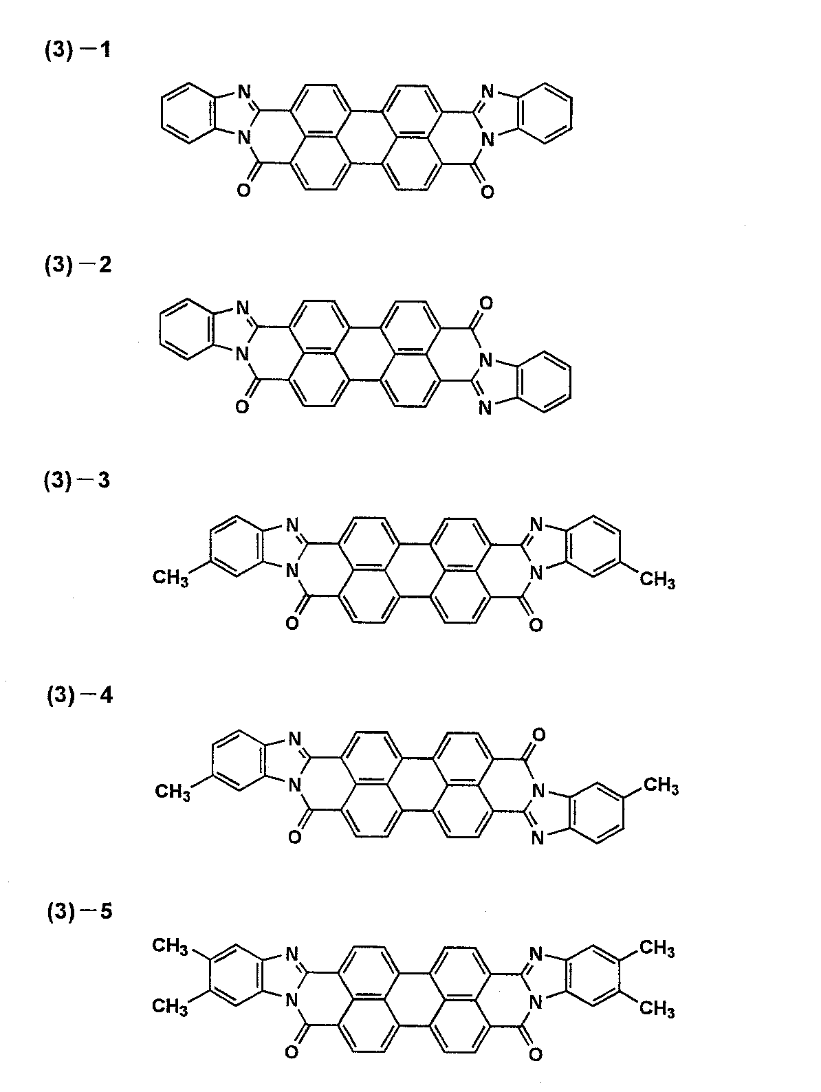
電荷発生物質としては、前記立体規則性を有した2,3−ブタンジオールのチタニルフタロシアニン付加体顔料と非付加体のチタニルフタロシアニン顔料の混晶(1つの顔料粒子中に付加体顔料と非付加体顔料が混在するという意味)を用いる。
【0039】
本発明のN型顔料の電荷発生物質としては、前記したN型特性を示す電荷発生物質であればいかなる種類の電荷発生物質でもよいが、その中でも特に好ましく用いられるN型顔料の電荷発生物質としては、ペリレン、1−ニトロペリレン、1,12−o−フェニレンペリレン、1,3,7,9−テトラアセトキシペリレンなどが挙げられるが、その中でも3,4,9,10−テトラカルボン酸イミド誘導体が好ましく、前記一般式(1)〜(3)の構造式で表されるものが特に好適に用いられる。
【0040】
構造としては対称または非対称のいずれでも良い。一般式(3)に見られるようにシス型とトランス型のものも含まれる。これらの異性体は合成またはその後の分離操作により単独で用いられる場合もあるし、合成時に混合体として生成したものをそのまま用いても良い。
【0041】
これらペリレン化合物の中でも特に一般式(3)で表されるペリレン化合物が最も好適に用いられ、中でも下記構造式で表されるペリレン化合物が最も好ましい。
【0042】
【化3】
(式中、Rは水素原子、ハロゲン原子、炭素数1〜10のアルキル基、アリール基、アルコキシ基、複素環基を表す。)
上記ペリレン化合物はいくつかの結晶多形が存在するが、特にどの結晶型のものも好適に用いられる。例えばX線回折スペクトルのブラッグ角2θ(±0.2°)の6.3°、12.4°、25.3°、27.1°にピークを有し、最大ピークが12.4°である結晶型のものやほとんど明瞭なピークを示さないアモルファスのものも含まれる。また、キャリア発生層に用いる場合には特定の結晶型を示すペリレンを分散して用いてもよいし、蒸着等の操作により膜を形成してもかまわない。また、蒸着膜を溶媒処理等で結晶変換させることもできる。
【0044】
次に、本発明に好ましく用いることの出来るペリレン化合物の具体例を下記に示す。
【0045】
一般式(1)の化合物の具体例
前記一般式(1)中、R1、R2は同一でも異なっていても良く、下記のものが挙げられる。
【0046】
【化4】
【化5】
【化6】
一般式(2)の化合物の具体例
前記一般式(2)中のR1は一般式(1)と同一であり、Zは下記のものが挙げられる。
【0050】
【化7】
2量体の場合には、Zは下記のものとなる。
【0052】
【化8】
一般式(3)の化合物
【0054】
【化9】
【化10】
【化11】
【化12】
【化13】
上記ペリレン顔料の他にN型顔料としては、電気陰性度が高い官能基、例えばシアノ基等を有するアゾ顔料や多環キノン顔料が挙げられる。
【0060】
従来のデジタル複写機等に主として用いられてきたP型のフタロシアニン顔料の電荷発生物質は、電荷キャリアの輸送能が小さいため、電荷発生層を厚くすると残留電位の上昇や光メモリによる画像むら等を発生しやすい。そのため電荷発生層を厚くして、電荷発生物質を増大し、感度の改善や光干渉縞を防止すること、或いは導電性基体からのフリーキャリアをブロックすることは困難であった。
【0061】
本発明の有機感光体は、導電性支持体上にP型顔料の電荷発生物質とN型顔料の電荷発生物質を含有する電荷発生層とその上に、電荷輸送物質を含有し、合計膜厚が5〜15μmである電荷輸送層を有する負帯電型有機感光体(負の静電潜像が形成される。)の構造を有しているが、電荷発生層の電荷発生物質はP型顔料とN型顔料を含有することにより、電荷発生層内で発生した電子は、比較的長い距離を移動し導電性基体に導通することができる。このため、電荷発生層を比較的厚い膜厚に構成しても、電子のトラップによる残留電位の上昇は防止される。又、電荷発生層が上記範囲の膜厚をもてば、十分に顔料濃度をあげることが出来るので、デジタル画像形成で、一般的に用いられる像露光光、レーザ光やLED光等の単波長光照射によるモアレ等の発生も防止することが出来る。その上、N型顔料が導電性基体からのフリーキャリアの注入効果が著しく、反転現像での黒ポチの発生を顕著に改善する。
【0062】
電荷発生層の膜厚は0.3〜2μmが好ましい。0.3μm未満では顔料濃度を十分に含有することができにくいため、露光電位の低下が不十分となり画像濃度が低下したり、レーザ光の干渉防止効果が小さくなったりしやすい。一方、2.0μmより大きいと、電荷発生層内での電荷キャリアのトラップ密度が大きくなりやすく、光メモリの増加による画像むらが発生しやすい。好ましい電荷発生層の膜厚は0.3〜1.0μmである。
【0063】
又、前記電荷発生層には、P型顔料とN型顔料の比率はP型顔料100質量部に対し、N型顔料10〜150質量部が好ましく、20〜130質量部がより好ましい。
【0066】
一方、電荷発生層の上には少なくとも1層以上の積層構成を有し、その膜厚の合計が5〜15μmの電荷輸送層を設けることを特徴とする。即ち、前記した電荷発生層の上に合計膜厚が5〜15μmの電荷輸送層を設けることにより、黒ポチが発生しにくく又白抜けの発生も防止され、文字画像及び中間調画像の両方とも、鮮鋭性が改良された電子写真画像を得ることが出来る。
【0067】
上記電荷発生層上の合計膜厚が5〜15μmの電荷輸送層の構造は、単層でもよく、複数の電荷輸送層から構成されていてもよい。又、単層又は複数の電荷輸送層の上に保護層を設けてもよい。複数の電荷輸送層で構成する場合は、最上層の電荷輸送層にフッ素系樹脂粒子を含有させた構成が好ましい。複数の電荷輸送層で構成した合計膜厚が5〜15μmの層構造は、電荷発生層で発生した電荷キャリアの拡散を小さくし、微細なドットで構成された潜像を十分な電位コントラストで再現することができる。該合計膜厚が5μm未満だと帯電電位が不十分になりやすく、15μmを超えると、該電荷キャリアの拡散が大きくなり、鮮鋭性が十分に改善されない。特に、電荷輸送層の合計膜厚を8〜14μmの範囲で構成した場合が、鮮鋭性の改善効果がより顕著である。
【0068】
前記最上層の電荷輸送層に含有されるフッ素系樹脂粒子とはフッ素原子を含有した樹脂粒子を意味し、例えば、四フッ化エチレン樹脂、三フッ化塩化エチレン樹脂、六フッ化エチレンプロピレン樹脂、フッ化ビニル樹脂、フッ化ビニリデン樹脂、二フッ化二塩化エチレン樹脂及びこれらの共重合体のなかから1種あるいは2種以上を適宜選択するのが好ましいが、特に、四フッ化エチレン樹脂及びフッ化ビニリデン樹脂が好ましい。フッ素系樹脂粒子の分子量や粒子の粒径は、適宜選択することができ、特に制限されるものではない。
【0069】
最上層の電荷輸送層はバインダー樹脂中にフッ素系樹脂粒子を含有する構成が好ましく、フッ素系樹脂粒子の割合は、粒子の粒径にも影響を受けるが、最上層全質量に対し、1〜50質量%であることが好ましく、より好ましくは5〜40質量%である。更に、最上層には電荷輸送物質が含有されていることが好ましい。
【0070】
本発明の最上層には、分散性、結着性や耐候性を向上させる目的でカップリング剤や酸化防止剤等の添加剤を加えてもよい。
【0071】
最上層のフッ素系樹脂粒子の分散方法としては、ホモジナイザー、ボールミル、サンドミル、ロールミル及び超音波といった方法が挙げられる。一次粒径の粒径まで分散可能であれば特に限定されるものではない。
【0072】
また、フッ素系樹脂粒子の分散助剤として、各種の界面活性剤、例えばクシ型グラフトポリマー等を適宜混合してもさしつかえない。
【0073】
最上層の膜厚は0.1〜4μmであることが好ましい。0.1μm未満では表面硬度や強度が十分でなく耐久性が低下し易く、4μmを超えると現像時に潜像によって形成されるコントラストポテンシャルが劣化し易い。より好ましくは0.2〜3.0μmである。
【0074】
最上層はクリーニング性及び耐汚染性を満足するために低表面エネルギーであることが好ましく、水の接触角で測定される低表面エネルギー性としては90度以上が好ましい。90度未満では電子写真プロセスによる繰り返し使用によって表面に帯電生成物やトナー、紙からもたらされる脱落物が付着し易く、クリーニング不良や表面抵抗の低下による潜像の劣化(画像流れ)を生じ易い。より好ましくは95度以上である。
【0075】
以上のような構成を採用することにより、鮮鋭性を著しく改善でき、且つ電荷輸送層を薄膜化した場合に発生しやすい、黒ポチの発生や画像むら等の画像欠陥を防止し、電位性能が安定した有機感光体を提供することができる。
【0076】
以下、上記以外の本発明に適用される有機感光体の構成について記載する。
本発明において、有機感光体とは電子写真感光体の構成に必要不可欠な電荷発生機能及び電荷輸送機能の少なくとも一方の機能を有機化合物に持たせて構成された電子写真感光体を意味し、公知の有機電荷発生物質又は有機電荷輸送物質から構成された感光体、電荷発生機能と電荷輸送機能を高分子錯体で構成した感光体等公知の有機感光体を全て含有する。
【0077】
本発明の電荷輸送層とは、光露光により電荷発生層で発生した電荷キャリアを有機感光体の表面に輸送する機能を有する層を意味し、該電荷輸送機能の具体的な検出は、電荷発生層と電荷輸送層を導電性支持体上に積層し、光導伝性を検知することにより確認することができる。
【0078】
本発明の有機感光体の層構成は、基本的には導電性支持体上に電荷発生層及び電荷輸送層の感光層から構成される。最も好ましい構成としては、感光層を電荷発生層と電荷輸送層で構成する。
【0079】
以下に本発明に用いられる具体的な感光体の構成について記載する。
導電性支持体
本発明の感光体に用いられる導電性支持体としてはシート状或いは円筒状の導電性支持体が用いられる。
【0080】
本発明の円筒状の導電性支持体とは回転することによりエンドレスに画像を形成できるに必要な円筒状の支持体を意味し、真直度で0.1mm以下、振れ0.1mm以下の範囲にある導電性の支持体が好ましい。この真直度及び振れの範囲を超えると、良好な画像形成が困難になる。
【0081】
導電性支持体の材料としてはアルミニウム、ニッケルなどの金属ドラム、又はアルミニウム、酸化錫、酸化インジュウムなどを蒸着したプラスチックドラム、又は導電性物質を塗布した紙・プラスチックドラムを使用することができる。導電性支持体としては常温で比抵抗103Ωcm以下が好ましい。
【0082】
本発明で用いられる導電性支持体は、その表面に封孔処理されたアルマイト膜が形成されたものを用いても良い。アルマイト処理は、通常例えばクロム酸、硫酸、シュウ酸、リン酸、硼酸、スルファミン酸等の酸性浴中で行われるが、硫酸中での陽極酸化処理が最も好ましい結果を与える。硫酸中での陽極酸化処理の場合、硫酸濃度は100〜200g/l、アルミニウムイオン濃度は1〜10g/l、液温は20℃前後、印加電圧は約20Vで行うのが好ましいが、これに限定されるものではない。又、陽極酸化被膜の平均膜厚は、通常20μm以下、特に10μm以下が好ましい。
【0083】
中間層
本発明においては導電性支持体と感光層の間に、バリヤー機能を備えた前記した中間層を設けることが好ましい。
【0084】
本発明の中間層には前記した吸水率が小さいバインダー樹脂中に酸化チタンを含有させることが好ましい。該酸化チタン粒子の平均粒径は、数平均一次粒径で10nm以上400nm以下の範囲が良く、15nm〜200nmが好ましい。
10nm未満では中間層によるモアレ発生の防止効果が小さい。一方、400nmより大きいと、中間層塗布液の酸化チタン粒子の沈降が発生しやすく、その結果中間層中の酸化チタン粒子の均一分散性が悪く、又黒ポチも増加しやすい。数平均一次粒径が前記範囲の酸化チタン粒子を用いた中間層塗布液は分散安定性が良好で、且つこのような塗布液から形成された中間層は黒ポチ発生防止機能の他、環境特性が良好で、且つ耐クラッキング性を有する。
【0085】
本発明に用いられる酸化チタン粒子の形状は、樹枝状、針状および粒状等の形状があり、このような形状の酸化チタン粒子は、例えば酸化チタン粒子では、結晶型としては、アナターゼ型、ルチル型及びアモルファス型等があるが、いずれの結晶型のものを用いてもよく、また2種以上の結晶型を混合して用いてもよい。その中でもルチル型で且つ粒状のものが最も良い。
【0086】
本発明の酸化チタン粒子は表面処理されていることが好ましく、表面処理の1つは、複数回の表面処理を行い、かつ該複数回の表面処理の中で、最後の表面処理が反応性有機ケイ素化合物を用いた表面処理を行うものである。また、該複数回の表面処理の中で、少なくとも1回の表面処理がアルミナ、シリカ、及びジルコニアから選ばれる少なくとも1種類以上の表面処理を行い、最後に反応性有機ケイ素化合物を用いた表面処理を行うことが好ましい。
【0087】
尚、アルミナ処理、シリカ処理、ジルコニア処理とは酸化チタン粒子表面にアルミナ、シリカ、或いはジルコニアを析出させる処理を云い、これらの表面に析出したアルミナ、シリカ、ジルコニアにはアルミナ、シリカ、ジルコニアの水和物も含まれる。又、反応性有機ケイ素化合物の表面処理とは、処理液に反応性有機ケイ素化合物を用いることを意味する。
【0088】
この様に、酸化チタン粒子の様な酸化チタン粒子の表面処理を少なくとも2回以上行うことにより、酸化チタン粒子表面が均一に表面被覆(処理)され、該表面処理された酸化チタン粒子を中間層に用いると、中間層内における酸化チタン粒子等の酸化チタン粒子の分散性が良好で、かつ黒ポチ等の画像欠陥を発生させない良好な感光体を得ることができるのである。
【0089】
上記反応性有機ケイ素化合物としては下記一般式(4)で表される化合物が挙げられるが、酸化チタン表面の水酸基等の反応性基と縮合反応をする化合物であれば、下記化合物に限定されない。
【0090】
一般式(4)
(R)n−Si−(X)4-n
(式中、Siはケイ素原子、Rは該ケイ素原子に炭素が直接結合した形の有機基を表し、Xは加水分解性基を表し、nは0〜3の整数を表す。)
一般式(4)で表される有機ケイ素化合物において、Rで示されるケイ素に炭素が直接結合した形の有機基としては、メチル、エチル、プロピル、ブチル、ペンチル、ヘキシル、オクチル、ドデシル等のアルキル基、フェニル、トリル、ナフチル、ビフェニル等のアリール基、γ−グリシドキシプロピル、β−(3,4−エポキシシクロヘキシル)エチル等の含エポキシ基、γ−アクリロキシプロピル、γ−メタアクリロキシプロピルの含(メタ)アクリロイル基、γ−ヒドロキシプロピル、2,3−ジヒドロキシプロピルオキシプロピル等の含水酸基、ビニル、プロペニル等の含ビニル基、γ−メルカプトプロピル等の含メルカプト基、γ−アミノプロピル、N−β(アミノエチル)−γ−アミノプロピル等の含アミノ基、γ−クロロプロピル、1,1,1−トリフロオロプロピル、ノナフルオロヘキシル、パーフルオロオクチルエチル等の含ハロゲン基、その他ニトロ、シアノ置換アルキル基を挙げられる。また、Xの加水分解性基としてはメトキシ、エトキシ等のアルコキシ基、ハロゲン基、アシルオキシ基が挙げられる。
【0091】
また、一般式(4)で表される有機ケイ素化合物は、単独でも良いし、2種以上組み合わせて使用しても良い。
【0092】
また、一般式(4)で表される有機ケイ素化合物の具体的化合物で、nが2以上の場合、複数のRは同一でも異なっていても良い。同様に、nが2以下の場合、複数のXは同一でも異なっていても良い。又、一般式(4)で表される有機ケイ素化合物を2種以上を用いるとき、R及びXはそれぞれの化合物間で同一でも良く、異なっていても良い。
【0093】
又、表面処理に用いる好ましい反応性有機ケイ素化合物としてはポリシロキサン化合物が挙げられる。該ポリシロキサン化合物の分子量は1000〜20000のものが一般に入手しやすく、又、黒ポチ発生防止機能も良好である。
【0094】
特にメチルハイドロジェンポリシロキサンを最後の表面処理に用いると良好な効果が得られる。
【0095】
感光層
電荷発生層
電荷発生層の電荷発生物質(CGM)は前記したP型顔料とN型顔料を併用する。
【0096】
電荷発生層にCGMの分散媒としてバインダーを用いる場合、バインダーとしては公知の樹脂を用いることができるが、最も好ましい樹脂としてはホルマール樹脂、ブチラール樹脂、シリコーン樹脂、シリコーン変性ブチラール樹脂、フェノキシ樹脂等が挙げられる。バインダー樹脂と電荷発生物質との割合は、バインダー樹脂100質量部に対し20〜600質量部が好ましい。これらの樹脂を用いることにより、繰り返し使用に伴う残留電位増加を最も小さくできる。
【0097】
電荷輸送層
前記したように、本発明では電荷輸送層を複数の電荷輸送層から構成し、且つ最上層の電荷輸送層にフッ素系樹脂粒子を含有させてもよい。
【0098】
電荷輸送層には電荷輸送物質(CTM)及びCTMを分散し製膜するバインダー樹脂を含有する。その他の物質としては必要により前記したフッ素系樹脂粒子や酸化防止剤等の添加剤を含有しても良い。
【0099】
電荷輸送物質(CTM)としては公知の正孔輸送性(P型)の電荷輸送物質(CTM)を用いる。例えばトリフェニルアミン誘導体、ヒドラゾン化合物、スチリル化合物、ベンジジン化合物、ブタジエン化合物などを用いることができる。これら電荷輸送物質は通常、適当なバインダー樹脂中に溶解して層形成が行われる。これらの中で繰り返し使用に伴う残留電位増加を最も小さくできるCTMは高移動度で、且つ組み合わされるCGMとのイオン化ポテンシャル差が0.5(eV)以下の特性を有するものであり、好ましくは0.30(eV)以下である。
【0100】
CGM、CTMのイオン化ポテンシャルは表面分析装置AC−1(理研計器社製)で測定される。
【0101】
電荷輸送層(CTL)に用いられるバインダー樹脂としては熱可塑性樹脂、熱硬化性樹脂いずれの樹脂かを問わない。例えばポリスチレン、アクリル樹脂、メタクリル樹脂、塩化ビニル樹脂、酢酸ビニル樹脂、ポリビニルブチラール樹脂、エポキシ樹脂、ポリウレタン樹脂、フェノール樹脂、ポリエステル樹脂、アルキッド樹脂、ポリカーボネート樹脂、シリコーン樹脂、メラミン樹脂並びに、これらの樹脂の繰り返し単位構造のうちの2つ以上を含む共重合体樹脂。又これらの絶縁性樹脂の他、ポリ−N−ビニルカルバゾール等の高分子有機半導体が挙げられる。これらの中で吸水率が小さく、CTMの分散性、電子写真特性が良好なポリカーボネート樹脂が最も好ましい。
【0102】
バインダー樹脂と電荷輸送物質との割合は、バインダー樹脂100質量部に対し50〜200質量部が好ましい。
【0103】
中間層、電荷発生層、電荷輸送層等の層形成に用いられる溶媒又は分散媒としては、n−ブチルアミン、ジエチルアミン、エチレンジアミン、イソプロパノールアミン、トリエタノールアミン、トリエチレンジアミン、N,N−ジメチルホルムアミド、アセトン、メチルエチルケトン、メチルイソプロピルケトン、シクロヘキサノン、ベンゼン、トルエン、キシレン、クロロホルム、ジクロロメタン、1,2−ジクロロエタン、1,2−ジクロロプロパン、1,1,2−トリクロロエタン、1,1,1−トリクロロエタン、トリクロロエチレン、テトラクロロエタン、テトラヒドロフラン、ジオキソラン、ジオキサン、メタノール、エタノール、ブタノール、イソプロパノール、酢酸エチル、酢酸ブチル、ジメチルスルホキシド、メチルセロソルブ等が挙げられる。本発明はこれらに限定されるものではないが、ジクロロメタン、1,2−ジクロロエタン、メチルエチルケトン等が好ましく用いられる。また、これらの溶媒は単独或いは2種以上の混合溶媒として用いることもできる。
【0104】
次に有機感光体を製造するための塗布加工方法としては、浸漬塗布、スプレー塗布、円形量規制型塗布等の塗布加工法が用いられるが、感光層の上層側の塗布加工は下層の膜を極力溶解させないため、又、均一塗布加工を達成するためスプレー塗布又は円形量規制型(円形スライドホッパ型がその代表例)塗布等の塗布加工方法を用いるのが好ましい。なお保護層は前記円形量規制型塗布加工方法を用いるのが最も好ましい。前記円形量規制型塗布については例えば特開昭58−189061号公報に詳細に記載されている。
【0105】
次に、本発明の有機感光体を用いた画像形成装置について説明する。
図1は本発明の有機感光体を用いた画像形成装置の断面概略図である。
【0106】
図1に示す画像形成装置1は、デジタル方式による画像形成装置であって、画像読取り部A、画像処理部B、画像形成部C、転写紙搬送手段としての転写紙搬送部Dから構成されている。
【0107】
画像読取り部Aの上部には原稿を自動搬送する自動原稿送り手段が設けられていて、原稿載置台11上に載置された原稿は原稿搬送ローラ12によって1枚宛分離搬送され読み取り位置13aにて画像の読み取りが行われる。原稿読み取りが終了した原稿は原稿搬送ローラ12によって原稿排紙皿14上に排出される。
【0108】
一方、プラテンガラス13上に置かれた場合の原稿の画像は走査光学系を構成する照明ランプ及び第1ミラーから成る第1ミラーユニット15の速度vによる読み取り動作と、V字状に位置した第2ミラー及び第3ミラーから成る第2ミラーユニット16の同方向への速度v/2による移動によって読み取られる。
【0109】
読み取られた画像は、投影レンズ17を通してラインセンサである撮像素子CCDの受光面に結像される。撮像素子CCD上に結像されたライン状の光学像は順次電気信号(輝度信号)に光電変換されたのちA/D変換を行い、画像処理部Bにおいて濃度変換、フィルタ処理などの処理が施された後、画像データは一旦メモリに記憶される。
【0110】
画像形成部Cでは、画像形成ユニットとして、像担持体であるドラム状の感光体21と、その外周に、該感光体21を帯電させる帯電手段(帯電工程)22、帯電した感光体の表面電位を検出する電位検出手段220、現像手段(現像工程)23、転写手段(転写工程)である転写搬送ベルト装置45、前記感光体21のクリーニング装置(クリーニング手段、クリーニング工程)26及び光除電手段(光所電荷発生工程)としてのPCL(プレチャージランプ)27が各々動作順に配置されている。また、現像手段23の下流側には感光体21上に現像されたパッチ像の反射濃度を測定する反射濃度検出手段222が設けられている。感光体21には、本発明の有機感光体を使用し、図示の時計方向に駆動回転される。
【0111】
回転する感光体21へは帯電手段22による一様帯電がなされた後、像露光手段(像露光工程)としての露光光学系30により画像処理部Bのメモリから呼び出された画像信号に基づいた像露光が行われる。書き込み手段である像露光手段としての露光光学系30は図示しないレーザダイオードを発光光源とし、回転するポリゴンミラー31、fθレンズ34、シリンドリカルレンズ35を経て反射ミラー32により光路が曲げられ主走査がなされるもので、感光体21に対してAoの位置において像露光が行われ、感光体21の回転(副走査)によって静電潜像が形成される。本実施の形態の一例では画像部に対して露光を行い静電潜像を形成する。
【0112】
本発明の有機感光体には、単位膜厚当たり25〜45V/μmの電界強度が得られる帯電電位を付与することが好ましく、更に30〜45V/μmの電界強度がより好ましい。例えば、導電性支持体上に中間層1.0μm、電荷発生層0.5μm、電荷輸送層10μm、合計11.5μmの絶縁性膜厚を有する感光体に35V/μmの電界強度をかける場合には、約400Vの帯電電位を付加することが好ましい。
【0113】
本発明の画像形成方法においては、感光体上に静電潜像を形成するに際し、像露光をスポット面積が2×10⁻⁹m2以下の露光ビームを用いて行うことが好ましい。このような小径のビーム露光を行っても、本発明の有機感光体は、該スポット面積に対応した画像を忠実に形成することができる。より好ましいスポット面積は、0.01×10⁻⁹〜1×10⁻⁹m2である。その結果400dpi(dpi:2.54cm当たりのドット数)以上で、256階調を実現するところのきわめて優れた画像品質を達成することができる。
【0114】
前記露光ビームのスポット面積とは該ビーム光の強度がピーク強度の1/e2以上の光強度に対応する面積で表される。
【0115】
用いられる露光ビームとしては半導体レーザを用いた走査光学系、及びLEDや液晶シャッター等の固体スキャナー等があり、光強度分布についてもガウス分布及びローレンツ分布等があるがそれぞれのピーク強度の1/e2までの部分をスポット面積とする。
【0116】
感光体21上の静電潜像は現像手段23によって反転現像が行われ、感光体21の表面に可視像のトナー像が形成される。本発明の画像形成方法では、該現像手段に用いられる現像剤には重合トナーを用いることを特徴とする。形状や粒度分布が均一な重合トナーを本発明の有機感光体と併用することにより、より鮮鋭性が良好な電子写真画像を得ることができる。
【0117】
ここで、重合トナーとは、トナー用バインダーの樹脂の生成とトナー形状がバインダー樹脂の原料モノマーの重合、及びその後の化学的処理により形成されて得られるトナーを意味する。より具体的には懸濁重合、乳化重合等の重合反応と必要により、その後に行われる粒子同士の融着工程を経て得られるトナーを意味する。
【0118】
重合トナーは原料モノマーを水系で均一に分散した後に重合させトナーを製造することから、トナーの粒度分布、及び形状が均一なトナーが得られる。
【0119】
重合トナーは、懸濁重合法や、必要な添加剤の乳化液を加えた液中にて単量体を乳化重合し、微粒の重合粒子を製造し、その後に、有機溶媒、凝集剤等を添加して会合する方法で製造することができる。会合の際にトナーの構成に必要な離型剤や着色剤などの分散液と混合して会合させて調製する方法や、単量体中に離型剤や着色剤などのトナー構成成分を分散した上で乳化重合する方法などがあげられる。ここで会合とは樹脂粒子および着色剤粒子が複数個融着することを示す。
【0120】
即ち、重合性単量体中に着色剤や必要に応じて離型剤、荷電制御剤、さらに重合開始剤等の各種構成材料を添加し、ホモジナイザー、サンドミル、サンドグラインダー、超音波分散機などで重合性単量体に各種構成材料を溶解あるいは分散させる。この各種構成材料が溶解あるいは分散された重合性単量体を分散安定剤を含有した水系媒体中にホモミキサーやホモジナイザーなどを使用しトナーとしての所望の大きさの油滴に分散させる。その後、攪拌機構が後述の攪拌翼である反応装置へ移し、加熱することで重合反応を進行させる。反応終了後、分散安定剤を除去し、濾過、洗浄し、さらに乾燥することでトナーを調製する。
【0121】
また、本発明のトナーを製造する方法として樹脂粒子を水系媒体中で会合あるいは融着させて調製する方法も挙げることができる。この方法としては、特に限定されるものではないが、例えば、特開平5−265252号公報や特開平6−329947号公報、特開平9−15904号公報に示す方法を挙げることができる。すなわち、樹脂粒子と着色剤などの構成材料の分散粒子、あるいは樹脂および着色剤等より構成される微粒子を複数以上会合させる方法、特に水中にてこれらを乳化剤を用いて分散した後に、臨界凝集濃度以上の凝集剤を加え塩析させると同時に、形成された重合体自体のガラス転移点温度以上で加熱融着させて融着粒子を形成しつつ徐々に粒径を成長させ、目的の粒径となったところで水を多量に加えて粒径成長を停止し、さらに加熱、攪拌しながら粒子表面を平滑にして形状を制御し、その粒子を含水状態のまま流動状態で加熱乾燥することにより、トナーを形成することができる。なお、ここにおいて凝集剤と同時に水に対して無限溶解する有機溶媒を加えてもよい。
【0122】
なお、本発明で用いられる形状係数等の均一なトナーを作製するための材料や製造方法、重合トナーの反応装置等については特開2000−214629に詳細に記載されている。
【0123】
転写紙搬送部Dでは、画像形成ユニットの下方に異なるサイズの転写紙Pが収納された転写紙収納手段としての給紙ユニット41(A)、41(B)、41(C)が設けられ、また側方には手差し給紙を行う手差し給紙ユニット42が設けられていて、それらの何れかから選択された転写紙Pは案内ローラ43によって搬送路40に沿って給紙され、給紙される転写紙Pの傾きと偏りの修正を行うレジストローラ対44によって転写紙Pは一時停止を行ったのち再給紙が行われ、搬送路40、転写前ローラ43a、給紙経路46及び進入ガイド板47に案内され、感光体21上のトナー画像が転写位置Boにおいて転写極24及び分離極25によって転写搬送ベルト装置45の転写搬送ベルト454に載置搬送されながら転写紙Pに転写され、該転写紙Pは感光体21面より分離し、転写搬送ベルト装置45により定着手段50に搬送される。
【0124】
定着手段50は定着ローラ51と加圧ローラ52とを有しており、転写紙Pを定着ローラ51と加圧ローラ52との間を通過させることにより、加熱、加圧によってトナーを定着させる。トナー画像の定着を終えた転写紙Pは排紙トレイ64上に排出される。
【0125】
以上は転写紙の片側への画像形成を行う状態を説明したものであるが、両面複写の場合は排紙切換部材170が切り替わり、転写紙案内部177が開放され、転写紙Pは破線矢印の方向に搬送される。
【0126】
更に、搬送機構178により転写紙Pは下方に搬送され、転写紙反転部179によりスイッチバックさせられ、転写紙Pの後端部は先端部となって両面複写用給紙ユニット130内に搬送される。
【0127】
転写紙Pは両面複写用給紙ユニット130に設けられた搬送ガイド131を給紙方向に移動し、給紙ローラ132で転写紙Pを再給紙し、転写紙Pを搬送路40に案内する。
【0128】
再び、上述したように感光体21方向に転写紙Pを搬送し、転写紙Pの裏面にトナー画像を転写し、定着手段50で定着した後、排紙トレイ64に排紙する。
【0129】
本発明の画像形成装置としては、上述の感光体と、現像器、クリーニング器等の構成要素をプロセスカートリッジとして一体に結合して構成し、このユニットを装置本体に対して着脱自在に構成しても良い。又、帯電器、像露光器、現像器、転写又は分離器、及びクリーニング器の少なくとも1つを感光体とともに一体に支持してプロセスカートリッジを形成し、装置本体に着脱自在の単一ユニットとし、装置本体のレールなどの案内手段を用いて着脱自在の構成としても良い。
【0130】
次に、本発明の画像形成方法に用いられるトナーについて説明する。
本発明の画像形成方法を用いてトナー像の形成の為に用いられるトナーは、
▲1▼トナー粒子の形状係数が1.2〜1.6の範囲にあるトナー粒子の割合が65個数%以上、
▲2▼角がないトナー粒子の割合が50個数%以上、
▲3▼トナー粒子の粒径をD(μm)とするとき、自然対数lnDを横軸にとり、この横軸を0.23間隔で複数の階級に分けた個数基準の粒度分布を示すヒストグラムにおける最頻階級に含まれるトナー粒子の相対度数(m1)と、前記最頻階級の次に頻度の高い階級に含まれるトナー粒子の相対度数(m2)との和(M)。即ち、本発明の画像形成方法では、前記した有機感光体に加え、現像剤のトナーとして、上記▲1▼〜▲3▼の少なくとも1つ以上の条件を満たしたトナーを含有した現像剤を用いることにより、トナー等による有機感光体の表面の汚染を防止し、反転現像における白ヌケや黒ポチ等の画像欠陥の発生を防止し、良好な電子写真画像を得ることができる。
【0131】
即ち、トナー自体の形状分布を均一化することにより、トナーの搬送性を向上させ、現像剤搬送部材などとの摩擦帯電を均一化させ、結果として現像領域での帯電量分布を狭くすることができ、薄層の感光層を有する本発明の有機感光体を用いて、高電界強度の画像形成条件でトナー像を形成しても、トナーの現像性や転写性を向上させ、白ヌケや筋状の画質欠陥の発生を防止することができる。
【0132】
又、本発明者等は鋭意検討した結果、角がないトナー粒子ではその表面の平滑性により、現像剤搬送部材などのトナーが接触する部位に対するストレスにより発生する微細な粒子の発生を抑制することができることと、その平滑な表面性により、摩擦帯電での過度な帯電性の蓄積が無いことから、有機感光体への過度の付着力の増加が防止され、転写性の劣化やクリーニング不良を防止し、白ヌケや筋状の画質欠陥の発生を防止することができる。
【0133】
又、トナー自体の粒度分布をシャープにすることにより、トナーの搬送性を向上させ、現像剤搬送部材などとの摩擦帯電を均一化させ、結果として現像領域での帯電量分布を狭くすることができ、現像性、転写性、クリーニング性を向上させ、白ヌケや筋状の画質欠陥の発生を防止することができる。
【0134】
本発明者等は、現像工程や転写工程或いはクリーニング工程では、画像形成を繰り返した場合には、形が不揃いなトナー粒子、角となる部分を有するトナー粒子、粒径が特に大きい或いは小さいトナーが問題となりやすい傾向となった。この理由については明確ではないが、トナー粒子の形が不揃いである場合にはトナが現像装置内部、或いは転写工程、クリーニング工程で、攪拌や摩擦等による機械的ストレスを受けやすく、過大なストレスが加わる部分が発生することによって、トナーが破壊され、有機感光体表面に付着し、クリーニング不良を発生させやすい微粉砕トナーが発生する為と考えられる。又、このようなストレスの加わり方の違いは、トナー粒子の粒径によっても異なり、粒子径の小さいものの方が、ストレスを受けた場合に問題があり、トナー粒子径が大きいものでは、このような問題は発生しにくくなるが、解像度等の画質が低下する問題が発生する。
【0135】
又、上記▲1▼〜▲3▼の全ての条件を満たしたトナーと前記した有機感光体、即ち、N型顔料及びP型顔料の電荷発生物質を含有する電荷発生層及び該電荷発生層上に合計膜厚が5〜15μmの少なくとも1層以上の電荷輸送層を有する有機感光体と併用することにより、白ヌケや黒ポチの画像欠陥を顕著に改善し、鮮鋭性が良好な電子写真画像を得ることができる。
【0136】
又、上記▲1▼〜▲3▼の条件以外に、下記の▲4▼、▲5▼の条件、形状係数のバラツキ、個数粒度分布のバラツキを小さくしたトナーを用いることが、より好ましい。
▲4▼トナー粒子の形状係数の変動係数が16%以下、
▲5▼トナー粒子の個数粒度分布における個数変動係数が27%以下、
以下、上記▲1▼〜▲5▼のトナーについて説明する。
【0137】
トナーの形状係数(=トナー粒子の形状係数)
トナー粒子の形状係数は、下記式により示されるものであり、トナー粒子の丸さの度合いを示す。
【0138】
形状係数=((最大径/2)2×π)/投影面積
ここに、最大径とは、トナー粒子の平面上への投影像を2本の平行線ではさんだとき、その平行線の間隔が最大となる粒子の幅をいう。また、投影面積とは、トナー粒子の平面上への投影像の面積をいう。
【0139】
本発明では、この形状係数は、走査型電子顕微鏡により2000倍にトナー粒子を拡大した写真を撮影し、ついでこの写真に基づいて「SCANNING IMAGE ANALYZER」(日本電子社製)を使用して写真画像の解析を行うことにより測定した。この際、100個のトナー粒子を使用して形状係数を上記算出式にて測定したものである。
【0140】
本発明のトナーは、この形状係数が1.2〜1.6の範囲にあるトナー粒子の割合を65個数%以上であり、好ましくは、70個数%以上である。
【0141】
本発明ではN型顔料及びP型顔料の電荷発生物質を含有する電荷発生層及び該電荷発生層上に合計膜厚が5〜15μmの少なくとも1層以上の電荷輸送層を有する有機感光体上に形成された潜像をこの形状係数が1.2〜1.6の範囲にあるトナー粒子の割合を65個数%以上含有する現像剤により現像することにより、白ヌケや黒ポチ等の画像欠陥の発生を防止し、クリーニング性が向上し、鮮鋭性の良好な電子写真画像が得られる。
【0142】
この形状係数を制御する方法は特に限定されるものではない。例えば、トナー粒子を熱気流中に噴霧する方法、トナー粒子を気相中において衝撃力による機械的エネルギーを繰り返して付与する方法、トナーを溶解しない溶媒中に添加し旋回流を付与する方法等により、形状係数を1.2〜1.6にしたトナー粒子を調製し、これを通常のトナー中へ本発明の範囲内になるように添加して調製する方法がある。また、いわゆる重合法トナーを調製する段階で全体の形状を制御し、形状係数を1.2〜1.6に調製したトナー粒子を同様に通常のトナーへ添加して調製する方法がある。
【0143】
上記方法の中では重合法トナーが製造方法として簡便である点と、粉砕トナーに比較して表面の均一性に優れる点等で好ましい。該重合法トナー(重合トナーとも云う)とはトナー用バインダーの樹脂の生成とトナー形状がバインダー樹脂の原料モノマーの重合と、必要により、その後の化学的処理により形成されるトナーを意味する。より具体的には懸濁重合、乳化重合等の重合反応と、必要により、その後に行われる粒子同士の融着工程を経て得られるトナーを意味する。
【0144】
重合トナーは原料モノマーを水系で均一に分散した後に重合させトナーを製造することから、トナーの粒度分布、及び形状が均一なトナーが得られる。
【0145】
トナーの形状係数の変動係数(=トナー粒子の形状係数の変動係数)
トナー粒子の「形状係数の変動係数」は下記式から算出される。
【0146】
変動係数=〔S/K〕×100(%)
〔式中、S1は100個のトナー粒子の形状係数の標準偏差を示し、Kは形状係数の平均値を示す。〕
本発明のトナーは、この形状係数の変動係数が16%以下であり、好ましくは14%以下である。
【0147】
本発明ではN型顔料及びP型顔料の電荷発生物質を含有する電荷発生層及び該電荷発生層上に合計膜厚が5〜15μmの少なくとも1層以上の電荷輸送層を有する有機感光体上に形成された潜像をこの形状係数の変動係数が16%以下であるトナーを用いた現像剤により現像することにより、白ヌケや黒ポチ等の画像欠陥の発生を防止し、クリーニング性が向上し、鮮鋭性の良好な電子写真画像が得られる。
【0148】
このトナーの形状係数および形状係数の変動係数を、極めてロットのバラツキなく均一に制御するために、トナーを構成する樹脂粒子(重合体粒子)を調製(重合)、当該樹脂粒子を融着、形状制御させる工程において、形成されつつあるトナー粒子(着色粒子)の特性をモニタリングしながら適正な工程終了時期を決めてもよい。
【0149】
モニタリングするとは、インラインに測定装置を組み込みその測定結果に基づいて、工程条件の制御をするという意味である。すなわち、形状などの測定をインラインに組み込んで、例えば樹脂粒子を水系媒体中で会合あるいは融着させることで形成する重合法トナーでは、融着などの工程で逐次サンプリングを実施しながら形状や粒径を測定し、所望の形状になった時点で反応を停止する。
【0150】
モニタリング方法としては、特に限定されるものではないが、フロー式粒子像分析装置FPIA−2000(東亜医用電子社製)を使用することができる。本装置は試料液を通過させつつリアルタイムで画像処理を行うことで形状をモニタリングできるため好適である。すなわち、反応場よりポンプなどを使用し、常時モニターし、形状などを測定することを行い、所望の形状などになった時点で反応を停止するものである。
【0151】
トナーの個数変動係数(=トナー粒子の個数変動係数)
トナー粒子の個数粒度分布および個数変動係数はコールターカウンターTA−IIあるいはコールターマルチサイザー(コールター社製)で測定されるものである。本発明においてはコールターマルチサイザーを用い、粒度分布を出力するインターフェース(日科機製)、パーソナルコンピューターを接続して使用した。
前記コールターマルチサイザーにおいて使用するアパーチャーとしては100μmのものを用いて、2μm以上のトナーの体積、個数を測定して粒度分布および平均粒径を算出した。個数粒度分布とは、粒子径に対するトナー粒子の相対度数を表すものであり、個数平均粒径とは、個数粒度分布におけるメジアン径を表すものである。トナー粒子の「個数粒度分布における個数変動係数」は下記式から算出される。
【0152】
個数変動係数=〔S/Dn〕×100(%)
〔式中、S2は個数粒度分布における標準偏差を示し、Dnは個数平均粒径(μm)を示す。〕
本発明のトナー粒子の個数変動係数は27%以下が好ましく、より好ましくは25%以下である。
【0153】
本発明ではN型顔料及びP型顔料の電荷発生物質を含有する電荷発生層及び該電荷発生層上に合計膜厚が5〜15μmの少なくとも1層以上の電荷輸送層を有する有機感光体上に形成された潜像をトナー粒子の個数変動係数は27%以下であるトナーを用いた現像剤により現像することにより、白ヌケや黒ポチ等の画像欠陥の発生を防止し、クリーニング性が向上し、鮮鋭性の良好な電子写真画像が得られる。
【0154】
本発明のトナーにおける個数変動係数を制御する方法は特に限定されるものではない。例えば、トナー粒子を風力により分級する方法も使用できるが、個数変動係数をより小さくするためには液中での分級が効果的である。この液中で分級する方法としては、遠心分離機を用い、回転数を制御してトナー粒子径の違いにより生じる沈降速度差に応じてトナー粒子を分別回収し調製する方法がある。
【0155】
特に懸濁重合法によりトナーを製造する場合、個数粒度分布における個数変動係数を27%以下とするためには分級操作が必須である。懸濁重合法では、重合前に重合性単量体を水系媒体中にトナーとしての所望の大きさの油滴に分散させることが必要である。すなわち、重合性単量体の大きな油滴に対して、ホモミキサーやホモジナイザーなどによる機械的な剪断を繰り返して、トナー粒子程度の大きさまで油滴を小さくすることとなるが、このような機械的な剪断による方法では、得られる油滴の個数粒度分布は広いものとなり、従って、これを重合してなるトナーの粒度分布も広いものとなる。このために分級操作が必須となる。
【0156】
角がないトナー粒子の割合
本発明のトナーを構成するトナー粒子中、角がないトナー粒子の割合は50個数%以上であることが必要とされ、この割合が70個数%以上であることが好ましい。
【0157】
本発明のトナーを構成するトナー粒子中、角がないトナー粒子の割合は50個数%以上であることが好ましく、更に好ましくは70個数%以上とされる。
【0158】
本発明ではN型顔料及びP型顔料の電荷発生物質を含有する電荷発生層及び該電荷発生層上に合計膜厚が5〜15μmの少なくとも1層以上の電荷輸送層を有する有機感光体上に形成された潜像を角がないトナー粒子の割合は50個数%以上であるトナーを用いた現像剤により現像することにより、白ヌケや黒ポチ等の画像欠陥の発生を防止し、クリーニング性が向上し、鮮鋭性の良好な電子写真画像が得られる。
【0159】
ここに、「角がないトナー粒子」とは、電荷の集中するような突部またはストレスにより摩耗しやすいような突部を実質的に有しないトナー粒子を言い、具体的には以下のトナー粒子を角がないトナー粒子という。すなわち、図2(a)に示すように、トナー粒子Tの長径をLとするときに、半径(L/10)の円Cで、トナー粒子Tの周囲線に対し1点で内側に接しつつ内側をころがした場合に、当該円CがトナーTの外側に実質的にはみださない場合を「角がないトナー粒子」という。「実質的にはみ出さない場合」とは、はみ出す円が存在する突起が1箇所以下である場合をいう。また、「トナー粒子の長径」とは、当該トナー粒子の平面上への投影像を2本の平行線ではさんだとき、その平行線の間隔が最大となる粒子の幅をいう。なお、図2(b)および(c)は、それぞれ角のあるトナー粒子の投影像を示している。
【0160】
角がないトナー粒子の割合の測定は次のようにして行った。先ず、走査型電子顕微鏡によりトナー粒子を拡大した写真を撮影し、さらに拡大して15,000倍の写真像を得る。次いでこの写真像について前記の角の有無を測定する。この測定を100個のトナー粒子について行った。
【0161】
角がないトナーを得る方法は特に限定されるものではない。例えば、形状係数を制御する方法として前述したように、トナー粒子を熱気流中に噴霧する方法、またはトナー粒子を気相中において衝撃力による機械的エネルギーを繰り返して付与する方法、あるいはトナーを溶解しない溶媒中に添加し、旋回流を付与することによって得ることができる。
【0162】
また、樹脂粒子を会合あるいは融着させることで形成する重合法トナーにおいては、融着停止段階では融着粒子表面には多くの凹凸があり、表面は平滑でないが、形状制御工程での温度、攪拌翼の回転数および攪拌時間等の条件を適当なものとすることによって、角がないトナーが得られる。これらの条件は、樹脂粒子の物性により変わるものであるが、例えば、樹脂粒子のガラス転移点温度以上で、より高回転数とすることにより、表面は滑らかとなり、角がないトナーが形成できる。
【0163】
トナー粒子の粒径
本発明のトナーの粒径は、個数平均粒径で3.0〜8.5μmのものが好ましい。この粒径は、重合法によりトナー粒子を形成させる場合には、後に詳述するトナーの製造方法において、凝集剤の濃度や有機溶媒の添加量、または融着時間、さらには重合体自体の組成によって制御することができる。
【0164】
個数平均粒径が3.0〜8.5μmであることにより、転写効率が高くなってハーフトーンの画質が向上し、細線やドット等の画質が向上する。
【0165】
本発明のトナーは、トナー粒子の粒径をD(μm)とするとき、自然対数lnDを横軸にとり、この横軸を0.23間隔で複数の階級に分けた個数基準の粒度分布を示すヒストグラムにおいて、最頻階級に含まれるトナー粒子の相対度数(m1)と、前記最頻階級の次に頻度の高い階級に含まれるトナー粒子の相対度数(m2)との和(M)が70%以上であるトナーである。
【0166】
本発明ではN型顔料及びP型顔料の電荷発生物質を含有する電荷発生層及び該電荷発生層上に合計膜厚が5〜15μmの少なくとも1層以上の電荷輸送層を有する有機感光体上に形成された潜像を相対度数(m1)と相対度数(m2)との和(M)が70%以上であるトナーを用いた現像剤により現像することにより、白ヌケや黒ポチ等の画像欠陥の発生を防止し、クリーニング性が向上し、鮮鋭性の良好な電子写真画像が得られる。
【0167】
本発明において、前記の個数基準の粒度分布を示すヒストグラムは、自然対数lnD(D:個々のトナー粒子の粒径)を0.23間隔で複数の階級(0〜0.23:0.23〜0.46:0.46〜0.69:0.69〜0.92:0.92〜1.15:1.15〜1.38:1.38〜1.61:1.61〜1.84:1.84〜2.07:2.07〜2.30:2.30〜2.53:2.53〜2.76・・・)に分けた個数基準の粒度分布を示すヒストグラムであり、このヒストグラムは、下記の条件に従って、コールターマルチサイザーにより測定されたサンプルの粒径データを、I/Oユニットを介してコンピュータに転送し、当該コンピュータにおいて、粒度分布分析プログラムにより作製されたものである。
〔測定条件〕
(1)アパーチャー:100μm
(2)サンプル調製法:電解液〔ISOTON R−11(コールターサイエンティフィックジャパン社製)〕50〜100mlに界面活性剤(中性洗剤)を適量加えて攪拌し、これに測定試料10〜20mgを加える。この系を超音波分散機にて1分間分散処理することにより調製する。
【0168】
トナーの製造方法
本発明のトナーは、少なくとも重合性単量体を水系媒体中で重合せしめて得られる重合トナーであることが好ましく、また、少なくとも樹脂粒子を水系媒体中で会合させて得られる重合トナーであることが好ましい。以下、本発明の重合トナー(以後、単にトナーとも云う)を製造する方法について詳細に説明する。
【0169】
重合トナーは、懸濁重合法や、必要な添加剤の乳化液を加えた液中(水系媒体中)にて単量体を乳化重合して微粒の重合体粒子(樹脂粒子)を調製し、その後に、有機溶媒、凝集剤等を添加して当該樹脂粒子を会合する方法で製造することができる。ここで「会合」とは、前記樹脂粒子が複数個融着することをいい、当該樹脂粒子と他の粒子(例えば着色剤粒子)とが融着する場合も含むものとする。
【0170】
尚、本発明で重合トナーとは、トナー用バインダーの樹脂の生成とトナー形状がバインダー樹脂の原料モノマーの重合と、必要によりその後の化学的処理により形成されるトナーを意味する。より具体的には懸濁重合、乳化重合等の重合反応と、必要によりその後に行われる粒子同士の融着工程を経て形成されるトナーを意味する。
【0171】
重合トナーを製造する方法の一例を示せば、重合性単量体中に着色剤や必要に応じて離型剤、荷電制御剤、さらに重合開始剤等の各種構成材料を添加し、ホモジナイザー、サンドミル、サンドグラインダー、超音波分散機などで重合性単量体に各種構成材料を溶解あるいは分散させる。この各種構成材料が溶解あるいは分散された重合性単量体を分散安定剤を含有した水系媒体中にホモミキサーやホモジナイザーなどを使用しトナーとしての所望の大きさの油滴に分散させる。その後、攪拌機構が後述の攪拌翼である反応装置(攪拌装置)へ移し、加熱することで重合反応を進行させる。反応終了後、分散安定剤を除去し、濾過、洗浄し、さらに乾燥することで重合トナーを調製する。
【0172】
なお、本発明でいうところの「水系媒体」とは、少なくとも水が50質量%以上含有されたものを示す。
【0173】
また、重合トナーを製造する方法として樹脂粒子を水系媒体中で会合あるいは融着させて調製する方法も挙げることができる。この方法としては、特に限定されるものではないが、例えば、特開平5−265252号公報や特開平6−329947号公報、特開平9−15904号公報に示す方法を挙げることができる。すなわち、樹脂粒子と着色剤などの構成材料の分散粒子、あるいは樹脂および着色剤等より構成される微粒子を複数以上会合させる方法、特に水中にてこれらを乳化剤を用いて分散した後に、臨界凝集濃度以上の凝集剤を加え塩析させると同時に、形成された重合体自体のガラス転移点温度以上で加熱融着させて融着粒子を形成しつつ徐々に粒径を成長させ、目的の粒径となったところで水を多量に加えて粒径成長を停止し、さらに加熱、攪拌しながら粒子表面を平滑にして形状を制御し、その粒子を含水状態のまま流動状態で加熱乾燥することにより、本発明のトナーを形成することができる。なお、ここにおいて凝集剤と同時に水に対して無限溶解する溶媒を加えてもよい。
【0174】
樹脂を構成する重合性単量体として使用されるものは、スチレン、o−メチルスチレン、m−メチルスチレン、p−メチルスチレン、α−メチルスチレン、p−クロロスチレン、3,4−ジクロロスチレン、p−フェニルスチレン、p−エチルスチレン、2,4−ジメチルスチレン、p−tert−ブチルスチレン、p−n−ヘキシルスチレン、p−n−オクチルスチレン、p−n−ノニルスチレン、p−n−デシルスチレン、p−n−ドデシルスチレンの様なスチレンあるいはスチレン誘導体、メタクリル酸メチル、メタクリル酸エチル、メタクリル酸n−ブチル、メタクリル酸イソプロピル、メタクリル酸イソブチル、メタクリル酸t−ブチル、メタクリル酸n−オクチル、メタクリル酸2−エチルヘキシル、メタクリル酸ステアリル、メタクリル酸ラウリル、メタクリル酸フェニル、メタクリル酸ジエチルアミノエチル、メタクリル酸ジメチルアミノエチル等のメタクリル酸エステル誘導体、アクリル酸メチル、アクリル酸エチル、アクリル酸イソプロピル、アクリル酸n−ブチル、アクリル酸t−ブチル、アクリル酸イソブチル、アクリル酸n−オクチル、アクリル酸2−エチルヘキシル、アクリル酸ステアリル、アクリル酸ラウリル、アクリル酸フェニル等の、アクリル酸エステル誘導体、エチレン、プロピレン、イソブチレン等のオレフィン類、塩化ビニル、塩化ビニリデン、臭化ビニル、フッ化ビニル、フッ化ビニリデン等のハロゲン系ビニル類、プロピオン酸ビニル、酢酸ビニル、ベンゾエ酸ビニル等のビニルエステル類、ビニルメチルエーテル、ビニルエチルエーテル等のビニルエーテル類、ビニルメチルケトン、ビニルエチルケトン、ビニルヘキシルケトン等のビニルケトン類、N−ビニルカルバゾール、N−ビニルインドール、N−ビニルピロリドン等のN−ビニル化合物、ビニルナフタレン、ビニルピリジン等のビニル化合物類、アクリロニトリル、メタクリロニトリル、アクリルアミド等のアクリル酸あるいはメタクリル酸誘導体がある。これらビニル系単量体は単独あるいは組み合わせて使用することができる。
【0175】
また、樹脂を構成する重合性単量体としてイオン性解離基を有するものを組み合わせて用いることがさらに好ましい。例えば、カルボキシル基、スルフォン酸基、リン酸基等の置換基を単量体の構成基として有するもので、具体的には、アクリル酸、メタクリル酸、マレイン酸、イタコン酸、ケイ皮酸、フマール酸、マレイン酸モノアルキルエステル、イタコン酸モノアルキルエステル、スチレンスルフォン酸、アリルスルフォコハク酸、2−アクリルアミド−2−メチルプロパンスルフォン酸、アシッドホスホオキシエチルメタクリレート、3−クロロ−2−アシッドホスホオキシプロピルメタクリレート等が挙げられる。
【0176】
さらに、ジビニルベンゼン、エチレングリコールジメタクリレート、エチレングリコールジアクリレート、ジエチレングリコールジメタクリレート、ジエチレングリコールジアクリレート、トリエチレングリコールジメタクリレート、トリエチレングリコールジアクリレート、ネオペンチルグリコールジメタクリレート、ネオペンチルグリコールジアクリレート等の多官能性ビニル類を使用して架橋構造の樹脂とすることもできる。
【0177】
これら重合性単量体はラジカル重合開始剤を用いて重合することができる。この場合、懸濁重合法では油溶性重合開始剤を用いることができる。この油溶性重合開始剤としては、2,2′−アゾビス−(2,4−ジメチルバレロニトリル)、2,2′−アゾビスイソブチロニトリル、1,1′−アゾビス(シクロヘキサン−1−カルボニトリル)、2,2′−アゾビス−4−メトキシ−2,4−ジメチルバレロニトリル、アゾビスイソブチロニトリル等のアゾ系またはジアゾ系重合開始剤、ベンゾイルパーオキサイド、メチルエチルケトンペルオキサイド、ジイソプロピルペルオキシカーボネート、クメンヒドロペルオキサイド、t−ブチルヒドロペルオキサイド、ジ−t−ブチルペルオキサイド、ジクミルペルオキサイド、2,4−ジクロロベンゾイルペルオキサイド、ラウロイルペルオキサイド、2,2−ビス−(4,4−t−ブチルペルオキシシクロヘキシル)プロパン、トリス−(t−ブチルペルオキシ)トリアジンなどの過酸化物系重合開始剤や過酸化物を側鎖に有する高分子開始剤などを挙げることができる。
【0178】
また、乳化重合法を用いる場合には水溶性ラジカル重合開始剤を使用することができる。水溶性重合開始剤としては、過硫酸カリウム、過硫酸アンモニウム等の過硫酸塩、アゾビスアミノジプロパン酢酸塩、アゾビスシアノ吉草酸およびその塩、過酸化水素等を挙げることができる。
【0179】
分散安定剤としては、リン酸三カルシウム、リン酸マグネシウム、リン酸亜鉛、リン酸アルミニウム、炭酸カルシウム、炭酸マグネシウム、水酸化カルシウム、水酸化マグネシウム、水酸化アルミニウム、メタケイ酸カルシウム、硫酸カルシウム、硫酸バリウム、ベントナイト、シリカ、アルミナ等を挙げることができる。さらに、ポリビニルアルコール、ゼラチン、メチルセルロース、ドデシルベンゼンスルフォン酸ナトリウム、エチレンオキサイド付加物、高級アルコール硫酸ナトリウム等の界面活性剤として一般的に使用されているものを分散安定剤として使用することができる。
【0180】
本発明において優れた樹脂としては、ガラス転移点が20〜90℃のものが好ましく、軟化点が80〜220℃のものが好ましい。ガラス転移点は示差熱量分析方法で測定されるものであり、軟化点は高化式フローテスターで測定することができる。さらに、これら樹脂としてはゲルパーミエーションクロマトグラフィーにより測定される分子量が数平均分子量(Mn)で1000〜100000、重量平均分子量(Mw)で2000〜1000000のものが好ましい。さらに、分子量分布として、Mw/Mnが1.5〜100、特に1.8〜70のものが好ましい。
【0181】
前記樹脂粒子を水系媒体中で会合させる際に使用される凝集剤としては特に限定されるものではないが、金属塩から選択されるものが好適に使用される。具体的には、一価の金属として例えばナトリウム、カリウム、リチウム等のアルカリ金属の塩、二価の金属として例えばカルシウム、マグネシウム等のアルカリ土類の金属塩、マンガン、銅等の二価の金属の塩、鉄、アルミニウム等の三価の金属の塩等が挙げられ、具体的な塩としては、塩化ナトリウム、塩化カリウム、塩化リチウム、塩化カルシウム、塩化亜鉛、硫酸銅、硫酸マグネシウム、硫酸マンガン等を挙げることができる。これらは組み合わせて使用してもよい。
【0182】
これらの凝集剤は臨界凝集濃度以上添加することが好ましい。この臨界凝集濃度とは、水性分散物の安定性に関する指標であり、凝集剤を添加して凝集が発生する濃度を示すものである。この臨界凝集濃度は、乳化された成分および分散剤自体によって大きく変化するものである。例えば、岡村誠三他著「高分子化学 17、601(1960)日本高分子学会編」等に記述されており、詳細な臨界凝集濃度を求めることができる。また、別な手法として、目的とする粒子分散液に所望の塩を濃度を変えて添加し、その分散液のζ(ゼータ)電位を測定し、この値が変化する塩濃度を臨界凝集濃度として求めることもできる。
【0183】
凝集剤の添加量は、臨界凝集濃度以上であればよいが、好ましくは臨界凝集濃度の1.2倍以上、さらに好ましくは、1.5倍以上添加することがよい。
【0184】
凝集剤と共に使用される「水に対して無限溶解する溶媒」としては、形成される樹脂を溶解させないものが選択される。具体的には、メタノール、エタノール、プロパノール、イソプロパノール、t−ブタノール、メトキシエタノール、ブトキシエタノール等のアルコール類、アセトニトリル等のニトリル類、ジオキサン等のエーテル類を挙げることができる。特に、エタノール、プロパノール、イソプロパノールが好ましい。
【0185】
この水に対して無限溶解する溶媒の添加量は、凝集剤を添加した重合体含有分散液に対して1〜100体積%が好ましい。
【0186】
なお、粒子形状を均一化させるためには、着色粒子を調製し、濾過した後に粒子に対して10質量%以上の水が存在したスラリーを流動乾燥させることが好ましいが、この際、特に重合体中に極性基を有するものが好ましい。この理由としては、極性基が存在している重合体に対して、存在している水が多少膨潤する効果を発揮するために、形状の均一化が特に図られやすいからであると考えられる。
【0187】
本発明のトナーは少なくとも樹脂と着色剤を含有するものであるが、必要に応じて定着性改良剤である離型剤や荷電制御剤等を含有することもできる。さらに、上記樹脂と着色剤を主成分とするトナー粒子に対して無機微粒子や有機微粒子等で構成される外添剤を添加したものであってもよい。
【0188】
本発明のトナーに使用する着色剤としてはカーボンブラック、磁性体、染料、顔料等を任意に使用することができ、カーボンブラックとしてはチャンネルブラック、ファーネスブラック、アセチレンブラック、サーマルブラック、ランプブラック等が使用される。磁性体としては鉄、ニッケル、コバルト等の強磁性金属、これらの金属を含む合金、フェライト、マグネタイト等の強磁性金属の化合物、強磁性金属を含まないが熱処理する事により強磁性を示す合金、例えばマンガン−銅−アルミニウム、マンガン−銅−錫等のホイスラー合金と呼ばれる種類の合金、二酸化クロム等を用いる事ができる。
【0189】
染料としてはC.I.ソルベントレッド1、同49、同52、同58、同63、同111、同122、C.I.ソルベントイエロー19、同44、同77、同79、同81、同82、同93、同98、同103、同104、同112、同162、C.I.ソルベントブルー25、同36、同60、同70、同93、同95等を用いる事ができ、またこれらの混合物も用いる事ができる。顔料としてはC.I.ピグメントレッド5、同48:1、同53:1、同57:1、同122、同139、同144、同149、同166、同177、同178、同222、C.I.ピグメントオレンジ31、同43、C.I.ピグメントイエロー14、同17、同93、同94、同138、C.I.ピグメントグリーン7、C.I.ピグメントブルー15:3、同60等を用いる事ができ、これらの混合物も用いる事ができる。数平均一次粒子径は種類により多様であるが、概ね10〜200nm程度が好ましい。
【0190】
着色剤の添加方法としては、乳化重合法で調製した重合体粒子を、凝集剤を添加することで凝集させる段階で添加し重合体を着色する方法や、単量体を重合させる段階で着色剤を添加し、重合し、着色粒子とする方法等を使用することができる。なお、着色剤は重合体を調製する段階で添加する場合はラジカル重合性を阻害しない様に表面をカップリング剤等で処理して使用することが好ましい。
【0191】
さらに、定着性改良剤としての低分子量ポリプロピレン(数平均分子量=1500〜9000)や低分子量ポリエチレン等を添加してもよい。
【0192】
荷電制御剤も同様に種々の公知のもので、且つ水中に分散することができるものを使用することができる。具体的には、ニグロシン系染料、ナフテン酸または高級脂肪酸の金属塩、アルコキシル化アミン、第4級アンモニウム塩化合物、アゾ系金属錯体、サリチル酸金属塩あるいはその金属錯体等が挙げられる。
【0193】
なお、これら荷電制御剤や定着性改良剤の粒子は、分散した状態で数平均一次粒子径が10〜500nm程度とすることが好ましい。
【0194】
本発明のトナーでは、外添剤として無機微粒子や有機微粒子などの微粒子を添加して使用することでより効果を発揮することができる。この理由としては、外添剤の埋没や脱離を効果的に抑制することができるため、その効果が顕著にでるものと推定される。
【0195】
この無機微粒子としては、シリカ、チタニア、アルミナ等の無機酸化物粒子の使用が好ましく、さらに、これら無機微粒子はシランカップリング剤やチタンカップリング剤等によって疎水化処理されていることが好ましい。疎水化処理の程度としては特に限定されるものでは無いが、メタノールウェッタビリティーとして40〜95のものが好ましい。メタノールウェッタビリティーとは、メタノールに対する濡れ性を評価するものである。この方法は、内容量200mlのビーカー中に入れた蒸留水50mlに、測定対象の無機微粒子を0.2g秤量し添加する。メタノールを先端が液体中に浸せきされているビュレットから、ゆっくり攪拌した状態で無機微粒子の全体が濡れるまでゆっくり滴下する。この無機微粒子を完全に濡らすために必要なメタノールの量をa(ml)とした場合に、下記式により疎水化度が算出される。
【0196】
疎水化度=(a/(a+50))×100
この外添剤の添加量としては、トナー中に0.1〜5.0質量%、好ましくは0.5〜4.0質量%である。また、外添剤としては種々のものを組み合わせて使用してもよい。
【0197】
いわゆる重合性単量体中に着色剤などのトナー構成成分を分散あるいは溶解したものを水系媒体中に懸濁し、ついで重合せしめてトナーを得る懸濁重合法トナーでは、重合反応を行う反応容器中での媒体の流れを制御することによりトナー粒子の形状を制御することができる。すなわち、形状係数が1.2以上の形状を有するトナー粒子を多く形成させる場合には、反応容器中での媒体の流れを乱流とし、重合が進行して懸濁状態で水系媒体中に存在している油滴が次第に高分子化することで油滴が柔らかい粒子となった時点で、粒子の衝突を行うことで粒子の合一を促進させ、形状が不定形となった粒子が得られる。また、形状係数が1.2より小さいほぼ球形のトナー粒子を形成させる場合には、反応容器中での媒体の流れを層流として、粒子の衝突を避けることによりほぼ球形の粒子が得られる。この方法により、トナー形状の分布を本発明の範囲内に制御できるものである。
【0198】
次に、重合トナーの製造に好ましく用いられる反応装置について説明する。図3および図4は、それぞれ、重合トナー反応装置の一例を示す斜視図および断面図である。図3および図4に示す反応装置において、熱交換用のジャケット1jを外周部に装着した縦型円筒状の攪拌槽2j内の中心部に回転軸3jを垂設し、該回転軸3jに攪拌槽2jの底面に近接させて配設された下段の攪拌翼40jと、より上段に配設された攪拌翼50jとが設けられている。上段の攪拌翼50jは、下段に位置する攪拌翼40jに対して回転方向に先行した交差角αをもって配設されている。本発明のトナーを製造する場合において、交差角αは90度(°)未満であることが好ましい。この交差角αの下限は特に限定されるものでは無いが、5°程度以上であることが好ましく、更に、好ましくは10°以上である。なお、三段構成の攪拌翼を設ける場合には、それぞれ隣接している攪拌翼間で交差角αが90度未満であることが好ましい。
【0199】
このような構成とすることで、上段に配設されている攪拌翼50jによりまず媒体が攪拌され、下側への流れが形成される。ついで、下段に配設された攪拌翼40jにより、上段の攪拌翼50jで形成された流れがさらに下方へ加速されるとともにこの攪拌翼50j自体でも下方への流れが別途形成され、全体として流れが加速されて進行するものと推定される。この結果、乱流として形成された大きなズリ応力を有する流域が形成されるために、得られるトナー粒子の形状を制御できるものと推定される。
【0200】
なお、図3および図4中、矢印は回転方向を示し、7jは上部材料投入口、8jは下部材料投入口、9jは攪拌を有効にするための乱流形成部材である。
【0201】
ここにおいて攪拌翼の形状については、特に限定はないが、方形板状のもの、翼の一部に切り欠きのあるもの、中央部に一つ以上の中孔部分、いわゆるスリットがあるものなどを使用することができる。これらの具体例を図5に記載する。
図5(a)に示す攪拌翼5aは中孔部のないもの、同図(b)に示す攪拌翼5bは中央に大きな中孔部6bがあるもの、同図(c)に示す攪拌翼5cは横長の中孔部6c(スリット)があるもの、同図(d)に示す攪拌翼5dは縦長の中孔部6d(スリット)があるものである。また、三段構成の攪拌翼を設ける場合において、上段の攪拌翼に形成される中孔部と、下段の攪拌翼に形成される中孔部とは異なるものであっても、同一のものであってもよい。
【0202】
なお、上記の構成を有する上段と下段の攪拌翼の間隙は特に限定されるものでは無いが、少なくとも攪拌翼の間に間隙を有していることが好ましい。この理由としては明確では無いが、その間隙を通じて媒体の流れが形成されるため、攪拌効率が向上するものと考えられる。但し、間隙としては、静置状態での液面高さに対して0.5〜50%の幅、好ましくは1〜30%の幅である。
【0203】
さらに、攪拌翼の大きさは特に限定されるものでは無いが、全攪拌翼の高さの総和が静置状態での液面高さの50%〜100%、好ましくは60%〜95%である。
【0204】
一方、樹脂粒子を水系媒体中で会合あるいは融着させる重合法トナーでは、融着段階での反応容器内の媒体の流れおよび温度分布を制御することで、さらには融着後の形状制御工程において加熱温度、攪拌回転数、時間を制御することで、トナー全体の形状分布および形状を任意に変化させることができる。
【0205】
すなわち、樹脂粒子を会合あるいは融着させる重合法トナーでは、反応装置内の流れを層流とし、内部の温度分布を均一化することができる攪拌翼および攪拌槽を使用して、融着工程および形状制御工程での温度、回転数、時間を制御することにより、所期の形状係数および均一な形状分布を有するトナーを形成することができる。この理由は、層流を形成させた場で融着させると、凝集および融着が進行している粒子(会合あるいは凝集粒子)に強いストレスが加わらず、かつ流れが加速された層流においては攪拌槽内の温度分布が均一である結果、融着粒子の形状分布が均一になるからであると推定される。さらに、その後の形状制御工程での加熱、攪拌により融着粒子は徐々に球形化し、トナー粒子の形状を任意に制御できる。
【0206】
樹脂粒子を会合あるいは融着させる重合法トナーを製造する際に使用される攪拌槽としては、前述の懸濁重合法と同様のものが使用できる。この場合、攪拌槽内には乱流を形成させるような邪魔板等の障害物を設けないことが必要である。
【0207】
この攪拌翼の形状についても、層流を形成させ、乱流を形成させないものであれば特に限定されないが、図5(c)に示した方形板状のもの等、連続した面により形成されるものが好ましく、曲面を有していてもよい。
【0208】
本発明のトナーは、例えば磁性体を含有させて一成分磁性トナーとして使用する場合、いわゆるキャリアと混合して二成分現像剤として使用する場合、非磁性トナーを単独で使用する場合等が考えられ、いずれも好適に使用することができるが、本発明ではキャリアと混合して使用する二成分現像剤として使用することが好ましい。
【0209】
本発明の有機感光体は電子写真複写機、レーザプリンター、LEDプリンター及び液晶シャッター式プリンター等の電子写真装置一般に適応するが、更に、電子写真技術を応用したディスプレー、記録、軽印刷、製版及びファクシミリ等の装置にも幅広く適用することができる。
【0210】
【実施例】
以下、実施例をあげて本発明を詳細に説明するが、本発明の様態はこれに限定されない。尚、下記文中「部」とは「質量部」を表す。
【0211】
感光体1の作製
下記の様に感光体1を作製した。
【0212】
円筒形アルミニウム支持体の表面を切削加工し、表面粗さRz=1.5(μm)の導電性支持体を用意した。
〈中間層〉
下記中間層分散液を同じ混合溶媒にて二倍に希釈し、一夜静置後に濾過(フィルター;日本ポール社製リジメッシュ5μmフィルター)し、中間層塗布液を作製した。
【0213】
【0214】
上記塗布液を用いて前記支持体上に、乾燥膜厚1.0μmとなるよう塗布した。
この塗布液を前記中間層の上に浸漬塗布法で塗布し、乾燥膜厚0.5μmの電荷発生層を形成した。
【0215】
【0216】
感光体2〜23の作製
感光体1の作製において、電荷発生層(CGL)中のP型顔料とN型顔料の種類及び量、膜厚、電荷輸送層1(CTL1)の電荷輸送物質(CTM)の種類、膜厚を表1のように変化させた以外は感光体1と同様にして感光体2〜23を作製した。但し、感光体4、14、19には前記電荷輸送層1の上に、更に下記の乾燥膜厚2μmの電荷輸送層2を設けた。
【0217】
【0218】
尚、上記電荷輸送層2中の4−フッ化エチレン樹脂粒子分散液は下記のようにして作製した。
【0219】
【0220】
【表1】
表1中、P型顔料及びN型顔料の種類を下記に示す。
P1:Cu−Kα特性X線の回折角度:ブラッグ角2θで、27.3°に最大なピークを有するチタニルフタロシアニン顔料
P2:(2R,3R)−2,3−ブタンジオールを付加したチタニルフタロシアニン顔料とチタニルフタロシアニン顔料の混晶
P3:(2S,3S)−2,3−ブタンジオールを付加したチタニルフタロシアニン顔料とチタニルフタロシアニン顔料の混晶
N1:例示化合物(3)−1と(3)−2の混晶
N2:例示化合物(3)−4
N3:例示化合物(3)−16
又、CTM1〜CTM2の化学構造を下記に示す。
【0222】
【化14】
現像剤の作製
トナー及び現像剤の作製
(トナー製造例1:乳化重合会合法の例)
n−ドデシル硫酸ナトリウム0.90kgと純水10.0リットルを入れ攪拌溶解した。この溶液に、リーガル330R(キャボット社製カーボンブラック)1.20kgを徐々に加え、1時間よく攪拌した後に、サンドグラインダー(媒体型分散機)を用いて、20時間連続分散した。このものを「着色剤分散液1」とする。
【0224】
また、ドデシルベンゼンスルホン酸ナトリウム0.055kgとイオン交換水4.0リットルとからなる溶液を「アニオン界面活性剤溶液A」とする。
【0225】
ノニルフェノールポリエチレンオキサイド10モル付加物0.014kgとイオン交換水4.0リットルとからなる溶液を「ノニオン界面活性剤溶液B」とする。
【0226】
過硫酸カリウム223.8gをイオン交換水12.0リットルに溶解した溶液を「開始剤溶液C」とする。
【0227】
温度センサー、冷却管、窒素導入装置を付けた容積100リットルのGL(グラスライニング)反応釜に、WAXエマルジョン(数平均分子量3000のポリプロピレンエマルジョン:数平均一次粒子径=120nm/固形分濃度=29.9%)3.41kgと「アニオン界面活性剤溶液A」全量と「ノニオン界面活性剤溶液B」全量とを入れ、攪拌を開始した。次いで、イオン交換水44.0リットルを加えた。
【0228】
加熱を開始し、液温度が75℃になったところで、「開始剤溶液C」全量を滴下して加えた。その後、液温度を75℃±1℃に制御しながら、スチレン12.1kgとアクリル酸n−ブチル2.88kgとメタクリル酸1.04kgとt−ドデシルメルカプタン548gとを滴下しながら投入した。滴下終了後、液温度を80℃±1℃に上げて、6時間加熱攪拌を行った。ついで、液温度を40℃以下に冷却し攪拌を停止し、ポールフィルターで濾過してラテックスを得た。これを「ラテックス−A」とする。
【0229】
なお、ラテックス−A中の樹脂粒子のガラス転移温度は57℃、軟化点は121℃、分子量分布は、重量平均分子量=1.27万、重量平均粒径は120nmであった。
【0230】
ドデシルベンゼンスルホン酸ナトリウム0.055kgをイオン交換純水4.0リットルに溶解した溶液を「アニオン界面活性剤溶液D」とする。
【0231】
また、ノニルフェノールポリエチレンオキサイド10モル付加物0.014kgをイオン交換水4.0リットルに溶解した溶液を「ノニオン界面活性剤溶液E」とする。
【0232】
過硫酸カリウム(関東化学社製)200.7gをイオン交換水12.0リットルに溶解した溶液を「開始剤溶液F」とする。
【0233】
温度センサー、冷却管、窒素導入装置、櫛形バッフルを付けた100リットルのGL反応釜に、WAXエマルジョン(数平均分子量3000のポリプロピレンエマルジョン:数平均一次粒子径=120nm/固形分濃度=29.9%)3.41kgと「アニオン界面活性剤溶液D」全量と「ノニオン界面活性剤溶液E」全量とを入れ、攪拌を開始した。
【0234】
次いで、イオン交換水44.0リットルを投入した。加熱を開始し、液温度が70℃になったところで、「開始剤溶液F」を添加した。ついで、スチレン11.0kgとアクリル酸n−ブチル4.00kgとメタクリル酸1.04kgとt−ドデシルメルカプタン9.02gとをあらかじめ混合した溶液を滴下した。滴下終了後、液温度を72℃±2℃に制御して、6時間加熱攪拌を行った。さらに、液温度を80℃±2℃に上げて、12時間加熱攪拌を行った。液温度を40℃以下に冷却し攪拌を停止した。ポールフィルターで濾過し、この濾液を「ラテックス−B」とする。
【0235】
なお、ラテックス−B中の樹脂粒子のガラス転移温度は58℃、軟化点は132℃、分子量分布は、重量平均分子量=24.5万、重量平均粒径は110nmであった。
【0236】
塩析剤としての塩化ナトリウム5.36kgをイオン交換水20.0リットルに溶解した溶液を「塩化ナトリウム溶液G」とする。
【0237】
フッ素系ノニオン界面活性剤1.00gをイオン交換水1.00リットルに溶解した溶液を「ノニオン界面活性剤溶液H」とする。
【0238】
温度センサー、冷却管、窒素導入装置、粒径および形状のモニタリング装置を付けた100リットルのSUS反応釜(図3に示した構成の反応装置、交差角αは25°)に、上記で作製したラテックス−A=20.0kgとラテックス−B=5.2kgと着色剤分散液1=0.4kgとイオン交換水20.0kgとを入れ攪拌した。ついで、40℃に加温し、塩化ナトリウム溶液G、イソプロパノール(関東化学社製)6.00kg、ノニオン界面活性剤溶液Hをこの順に添加した。その後、10分間放置した後に、昇温を開始し、液温度85℃まで60分で昇温し、85±2℃にて0.5〜3時間加熱攪拌して塩析/融着させながら粒径成長させた(塩析/融着工程)。次に純水2.1リットルを添加して粒径成長を停止させ、融着粒子分散液を作製した。
【0239】
温度センサー、冷却管、粒径および形状のモニタリング装置を付けた5リットルの反応容器(図3に示した構成の反応装置、交差角αは20°)に、上記で作製した融着粒子分散液5.0kgを入れ、液温度85℃±2℃にて、0.5〜15時間加熱攪拌して形状制御した(形状制御工程)。その後、40℃以下に冷却し攪拌を停止した。次に遠心分離機を用いて、遠心沈降法により液中にて分級を行い、目開き45μmの篩いで濾過し、この濾液を会合液とする。ついで、ヌッチェを用いて、会合液よりウェットケーキ状の非球形状粒子を濾取した。その後、イオン交換水により洗浄した。この非球形状粒子をフラッシュジェットドライヤーを用いて吸気温度60℃にて乾燥させ、ついで流動層乾燥機を用いて60℃の温度で乾燥させた。得られた着色粒子の100質量部に、シリカ微粒子1質量部をヘンシェルミキサーにて外添混合して乳化重合会合法によるトナーを得た。
【0240】
前記塩析/融着工程および形状制御工程のモニタリングにおいて、攪拌回転数、および加熱時間を制御することにより、形状および形状係数の変動係数を制御し、さらに液中分級により、粒径および粒度分布の変動係数を任意に調製して、表2に示す形状特性および粒度分布特性を有するトナー粒子からなるトナー1〜10を得た。
【0241】
【表2】
〔現像剤の製造〕
トナー1〜10の各々10質量部と、スチレン−メタクリレート共重合体で被覆した45μmフェライトキャリア100質量部とを混合することにより、評価用の現像剤1〜10を製造した。
【0243】
評価1(感光体1〜23の評価)
以上のようにして得た感光体1〜23と現像剤1を表3のように組み合わせ、各組み合わせをコニカ(株)製の反転現像方式デジタル複写機「Konica7060」改造機(スコロトロン帯電器、半導体レーザ像露光器(波長680nm)、反転現像手段を有するA4紙60枚/分機)に搭載し、下記評価項目について評価した。評価は、評価項目毎に、環境条件(温湿度条件)を変えて行なった。評価は、基本的に画素率が7%の文字画像、ハーフトーン画像、ベタ白画像、ベタ黒画像がそれぞれ1/4等分にあるオリジナル画像をA4で1枚間欠モードにて1万枚の複写を行い、評価した。但し各感光体の帯電条件は、単位膜厚当たり35〜45V/μmの電界強度が得られる帯電電位を付加して評価した。評価結果を表3に示す。
【0244】
評価条件
感光体のラインスピード;370mm/秒
帯電条件
帯電器;スコロトロン帯電器(負帯電)
帯電電位;単位膜厚当たり35V〜45V/μmの電界強度が得られる帯電電位を付加した。例えば、感光体1の中間層1.0μm、電荷発生層0.5μm、電荷輸送層13μm、合計膜厚14.5μmの絶縁性膜厚を有する感光体に35V/μmの電界強度をかける場合には、508Vの帯電電位を付加した。合計膜厚が小さい感光体ほど帯電電位を大きくするため、電界強度が高い帯電電位を付与した。
【0245】
露光条件
べた黒画像電位を−50Vにする露光量に設定。
【0246】
露光条件
べた黒画像電位を−50Vにする露光量に設定。
【0247】
露光ビーム:半導体レーザで、ドット密度400dpiの像露光を行った。
現像条件
現像剤は、現像剤1現像剤を使用した。
【0248】
転写条件:静電転写
クリーニング条件:クリーニングブレードを使用
評価項目及び評価方法
低温低湿(10℃20%RH)環境下の感度(べた黒画像部の電位変化)
低温低湿(10℃20%RH)環境下で、画素率が7%の文字画像、ハーフトーン画像、ベタ白画像、ベタ黒画像がそれぞれ1/4等分にあるオリジナル画像をA4で1枚間欠モードにて1万枚の複写を行い、初期と1万枚後の現像位置でのべた黒画像部の電位変化(|ΔV|)を評価した。|ΔV|が小さい方が低温低湿(10℃20%RH)環境下の感度が優れ、残留電位の上昇が少ない。
【0249】
◎;べた黒画像部の電位変化|ΔV|が50V未満(良好)
○;べた黒画像部の電位変化|ΔV|が50V〜150V(実用上問題なし)
×;べた黒画像部の電位変化|ΔV|が150Vより大きい(実用上問題有り)
文字細り(低温低湿(10℃20%RH)の環境下)
0.1mm、0.2mm幅の線画像が印刷されたオリジナル画像を複写し、評価した。
【0250】
◎;複写画像の線幅がオリジナル画像の線幅の75%以上で再現されている(良好)
○;複写画像の線幅がオリジナル画像の線幅の40%〜74%で再現されている(実用上問題ないレベル)
×;複写画像の線幅がオリジナル画像の線幅の39%以下、又は線幅が切断されている(実用上問題となるレベル)
ブラックスポット(高温高湿(30℃80%RH))
ハーフトーン画像上のブラックスポット(苺状のスポット画像)の発生状況を下記の基準で判定した。
【0251】
◎;感光体上にブラックスポットの発生核がみられず、ハーフトーン画像にもブラックスポットの発生なし(良好)
○;感光体上にブラックスポットの発生核がみられるが、ハーフトーン画像にはブラックスポットの発生なし(実用上問題なし)
×;感光体上にブラックスポットの発生核がみられ、ハーフトーン画像にもブラックスポットが発生している(実用上問題有り)
周期性の画像欠陥(高温高湿(30℃80%RH))
周期性が感光体の周期と一致し、目視できる白ヌケ、黒ポチ、筋状の画像欠陥が、A4サイズ当たり何個あるかで判定した。
【0252】
◎;0.4mm以上の画像欠陥の頻度:全ての複写画像が5個/A4以下(良好)
○;0.4mm以上の画像欠陥の頻度:6個/A4以上、10個/A4以下が1枚以上発生(実用上問題なし)
×;0.4mm以上の画像欠陥の頻度:11個/A4以上が1枚以上発生(実用上問題有り)
画像濃度(低温低湿(10℃20%RH))
画像濃度はべた黒部をマクベス社製RD−918を使用し反射濃度で測定した。相対濃度(複写していないA4紙の濃度を0.00とする)で評価した。
【0253】
◎;1.2以上(良好)
○;1.2未満〜0.8(実用上問題ないレベル)
×;0.8未満(実用上問題となるレベル)
カブリ(低温低湿(10℃20%RH))
カブリ濃度はべた白をマクベス社製RD−918を使用し反射濃度で測定した。相対濃度(複写していないA4紙の濃度を0.000とする)で評価した。
【0254】
◎;濃度が0.010未満(良好)
○;0.010〜0.020(実用上問題ないレベル)
×;0.020より大(実用上問題となるレベル)
鮮鋭性
画像の鮮鋭性は、低温低湿(10℃20%RH)、高温高湿(30℃80%RH)の両環境において画像を出し評価した。3ポイント、5ポイントの文字画像を形成し、下記の判断基準で評価した。
【0255】
◎;3ポイント、5ポイントとも明瞭であり、容易に判読可能
○;3ポイントは一部判読不能、5ポイントは明瞭であり、容易に判読可能
×;3ポイントは殆ど判読不能、5ポイントも一部あるいは全部が判読不能
【0256】
【表3】
表3から明らかなように、本発明の有機感光体12〜16、19(導電性支持体上にN型顔料及び立体規則性を有した2,3−ブタンジオールのチタニルフタロシアニン付加体顔料を含むP型顔料の電荷発生物質を混合して同一層に含有する電荷発生層及び該電荷発生層上に合計膜厚が5〜15μmの少なくとも1層以上の電荷輸送層を有することを特徴とする有機感光体)は、低温低湿(10℃20%RH)環境下の感度(べた黒画像部の電位変化)が優れ、このため低温低湿下の文字細りもなく、しかも、周期性画像欠陥の発生もなく、画像濃度、カブリ、鮮鋭性に優れた特性を示している。中でも、P型顔料とN型顔料の比率が5/1〜1/1.3の範囲にあり、N型顔料が一般式(3)のペリレン顔料で、且つ電荷輸送層の膜厚が8〜14μmの範囲にある感光体14、15、19は改善効果が著しい。一方、本発明外の電荷発生物質を用いた感光体20〜23では、低温低湿(10℃20%RH)環境下の感度が劣り、文字細りを発生しており、感光体21、22ではカブリも発生している。又電荷輸送層の膜厚が5μm未満の感光体10では、低温低湿(10℃20%RH)環境下の感度が劣り、文字細りを発生し、周期性の画像欠陥の発生が著しく、電荷輸送層の膜厚が15μmより厚い感光体11は文字細りが発生し、いずれも鮮鋭性が低下している。
【0260】
評価3(現像剤の変化)
前記感光体1及び19と現像剤2〜10を表4のように組み合わせ、各組み合わせ(組み合わせNo.1〜18)をコニカ(株)製の反転現像方式デジタル複写機「Konica7060」改造機(スコロトロン帯電器、半導体レーザ像露光器(波長680nm)、反転現像手段を有するA4紙60枚/分機)に搭載し、前記評価1と同様の評価を行なった。評価結果を表4に示す。
【0261】
【表4】
表4から明らかなように、本発明の有機感光体とトナーを用いた組み合わせ1〜8及び10〜17は、低温低湿(10℃20%RH)環境下の感度(べた黒画像部の電位変化)が優れ、このため低温低湿下の文字細りもなく、しかも、ブッラクスポット、周期性画像欠陥等の発生もなく、画像濃度、カブリ、鮮鋭性に優れた特性を示している。一方、感光体は本発明内の感光体であっても、現像剤が本発明外の組み合わせ、即ち、下記▲1▼〜▲3▼の条件を1つも満たしていない組み合わせ9、18は、文字細り、周期性の画像欠陥等が発生し、鮮鋭性を劣化させている。
【0263】
▲1▼トナー粒子の形状係数が1.2〜1.6の範囲にあるトナー粒子の割合が65個数%以上、
▲2▼角がないトナー粒子の割合が50個数%以上、
▲3▼トナー粒子の粒径をD(μm)とするとき、自然対数lnDを横軸にとり、この横軸を0.23間隔で複数の階級に分けた個数基準の粒度分布を示すヒストグラムにおける最頻階級に含まれるトナー粒子の相対度数(m1)と、前記最頻階級の次に頻度の高い階級に含まれるトナー粒子の相対度数(m2)との和(M)が70%以上。
【0264】
【発明の効果】
本発明の有機感光体、及び該有機感光体を用いたプロセスカートリッジ、画像形成方法及び画像形成装置を用いることにより、低温低湿環境で発生しやすい感度不良に伴う画像不良と高温高湿で発生しやすい画像欠陥を防止し、画像濃度、鮮鋭性が良好な電子写真画像を提供することができる。
【図面の簡単な説明】
【図1】本発明の有機感光体を用いた画像形成装置の断面概略図である。
【図2】(a)は、角のないトナー粒子の投影像を示す説明図であり、(b)および(c)は、それぞれ角のあるトナー粒子の投影像を示す説明図である。
【図3】重合トナー反応装置の一例を示す斜視図である。
【図4】重合トナー反応装置の一例を示す断面図である。
【図5】攪拌翼の形状の具体例を示す概略図である。
【符号の説明】
1 画像形成装置
21 感光体
22 帯電手段
23 現像手段
24 転写極
25 分離極
26 クリーニング装置
30 露光光学系
45 転写搬送ベルト装置
50 定着手段
250 分離爪ユニット[0001]
BACKGROUND OF THE INVENTION
The present invention relates to an organic photoreceptor (hereinafter also simply referred to as a photoreceptor) used for electrophotographic image formation, a process cartridge, an image forming apparatus, and an image forming method. More specifically, the present invention is used in the fields of copiers and printers. The present invention relates to an organic photosensitive member, a process cartridge, an image forming apparatus, and an image forming method used for electrophotographic image formation.
[0002]
[Prior art]
Electrophotographic photoconductors offer great advantages such as wider selection of materials, better environmental suitability and lower production costs than inorganic photoconductors such as selenium and amorphous silicon photoconductors. In recent years, organic photoreceptors have become the mainstream in place of inorganic photoreceptors.
[0003]
On the other hand, in recent electrophotographic image forming methods, as a hard copy printer of a personal computer, and in an ordinary copying machine, image processing of LEDs and lasers is easy due to the ease of image processing and deployment to a multifunction machine. A digital image forming system that uses a light source has rapidly spread. Furthermore, a technique for producing a high-quality electrophotographic image by developing a finer digital image has been developed. For example, image exposure is performed with a laser beam with a small spot area, the density of the dot latent image is increased to form a high-definition latent image, the latent image is developed with a small particle size toner, and a high-quality electrophotographic image The technology for producing is disclosed. (Patent Document 1)
Further, in order to faithfully reproduce a high-definition electrostatic latent image, it is necessary to ensure a sufficient potential contrast in the exposed / unexposed area. It is important to suppress carrier diffusion until the surface charge is reached. The latent image degradation of the high-density image is caused by the effect of diffusion to the electrostatic latent image cannot be ignored when the ratio D / μ of the diffusion constant (D) and the drift mobility (μ) of the charge transport layer increases. It has been reported that latent image degradation increases as the layer thickness increases (Non-Patent Document 1).
[0004]
An electrophotographic photosensitive member that has a thin charge transport layer and prevents diffusion of an electrostatic latent image has already been proposed in patents (Patent Document 2). However, when these proposed organophotoreceptors are actually used to form an image using an electrophotographic image forming apparatus, a blurred image with a reduced image density tends to appear. The cause of this is that when the organic photoreceptor is thinned, the electrostatic capacity of the photosensitive layer is reduced, it is difficult to obtain a sufficient image potential (difference between the charged potential and the residual potential), and the image density tends to decrease. In particular, when a developer using a small particle size toner is used in order to obtain high image quality, developability is lowered, image density in reversal development is not sufficient, and character images and photographic images with good sharpness are obtained. The problem of being difficult to occur has occurred.
[0005]
In order to recover this decrease in developability, it is effective to increase the electric field intensity per unit thickness of the photosensitive member by applying a charge with an increased amount of charge per unit area to the thinned organic photosensitive member. . However, if the electric field strength per unit thickness of the photoconductor is increased, the charging potential may decrease due to repeated use, or the photoconductor may be insufficiently sensitive in a low temperature and low humidity environment. Are likely to increase, and periodic image defects such as black spots and white spots are likely to occur.
[0006]
In order to solve the problem of insufficient sensitivity of the thinned photoreceptor, the organic photoreceptor has a layer structure in which the photosensitive layer is functionally separated into a charge generation layer and a charge transport layer, and the charge transport layer has a molecular weight of 500. A structure containing a large amount of charge transporting substances having low and high molecular weights before and after is effective.
[0007]
However, in the charge transport layer having such a configuration, the lack of sensitivity in a low-temperature and low-humidity environment is improved to some extent, but the film quality is lowered, and the charge transport layer on the surface layer is easily contaminated with foreign substances. That is, the surface of the photosensitive member is easily contaminated with paper dust or a toner composition by a developing unit, a transferring unit, a cleaning unit, and the like disposed around the photosensitive member, and as a result, the period of black spots (spot-like spot images) Image defects are likely to occur.
[0008]
In order to prevent contamination of the surface of the photoreceptor, an organic photoreceptor having a surface layer containing fluorine resin particles has been proposed (Patent Document 3). However, an organic photoreceptor containing fluorine resin particles tends to cause image blur. Also, the mechanical strength of the surface layer is likely to be lowered, and the surface of the photoreceptor is easily worn by contact friction with the cleaning means or the like, and a good electrophotographic image cannot always be provided.
[0009]
[Patent Document 1]
Japanese Patent Laid-Open No. 2001-255585
[0010]
[Patent Document 2]
JP-A-5-119503
[0011]
[Patent Document 3]
JP-A-63-65449
[0012]
[Non-Patent Document 1]
Journal of the Imaging Society of Japan Vol. 38, No. 4, 296
[0013]
[Problems to be solved by the invention]
An object of the present invention is to solve the above-described problems, and to provide an organic photoreceptor having good potential stability and good image quality. That is, it is to provide an organic photoreceptor having good potential stability and capable of faithfully developing an electrostatic latent image as a toner image, and preventing image defects such as black spots and white spots, and image density. Another object of the present invention is to provide an organic photoreceptor capable of ensuring high quality image quality with good sharpness and gradation, and an image forming method and an image forming apparatus using the organic photoreceptor.
[0014]
[Means for Solving the Problems]
As a result of repeated studies on the above problems, in order to obtain a good electrophotographic image with improved sharpness using an organic photoreceptor, the organic photoreceptor has a functional separation structure of a charge generation layer and a charge transport layer. Reduce the thickness of the charge transport layer that forms the surface layer, prevent carrier diffusion, and at the same time prevent fluctuations in charge potential and sensitivity, reducing image density, causing fogging, periodic image defects, etc. It is necessary to prevent. For that purpose, it is important to reduce the thickness of the charge transport layer, stabilize the charging potential, prevent the residual power increase and the fluctuation of sensitivity due to repetition, and at the same time prevent the injection of free carriers from the conductive substrate. As a result, the present invention has been completed.
[0015]
That is, the inventors of the present invention have an organic photoreceptor having a functional separation structure of a charge generation layer and a charge transport layer on a conductive support, and the charge generation material of the charge generation layer contains free carriers from the conductive support. It has been found that the above-mentioned problems of the present invention can be solved by using an organic pigment that can block the injection of water and has excellent potential stability and high sensitivity.
[0016]
That is, the object of the present invention is achieved by having the following configuration.
1. On the conductive supportIt is a mixed crystal of compound (3) -1 and compound (3) -2P-type mixed crystal of N-type pigment, titanyl phthalocyanine pigment added with (2R, 3R) -2,3-butanediol or (2S, 3S) -2,3-butanediol and non-adducted titanyl phthalocyanine pigment A charge generation layer containing a charge generation material mixed with a pigment and contained in the same layer, and at least one layer containing a hole transporting charge transport material on the charge generation layer and having a total film thickness of 5 to 15 μm An organic photoreceptor having the above charge transport layer.
[0017]
2.2. The charge generation layer according to 1, wherein the charge generation layer has a thickness of 0.3 to 2.0 μm.Organic photoreceptor.
[0021]
3. The N-type pigment is 10 to 150 parts by mass per 100 parts by mass of the P-type pigment.1 or 2The organic photoreceptor described in 1.
[0022]
4). Organic photoreceptor and charging means for uniformly charging the organic photoreceptor, image exposing means for forming an electrostatic latent image on the organic photoreceptor, developing means for developing the electrostatic latent image on the organic photoreceptor And at least one of transfer means for transferring the toner image visualized on the organic photoreceptor onto a transfer material and cleaning means for removing residual toner on the organic photoreceptor after transfer. In the process cartridge supported by the image forming apparatus and detachably attachable to the main body of the image forming apparatus, the organic photoreceptor is disposed on the conductive support.It is a mixed crystal of compound (3) -1 and compound (3) -2P-type mixed crystal of N-type pigment, titanyl phthalocyanine pigment added with (2R, 3R) -2,3-butanediol or (2S, 3S) -2,3-butanediol and non-adducted titanyl phthalocyanine pigment A charge generation layer containing a charge generation material mixed with a pigment and contained in the same layer, and at least one layer containing a hole transporting charge transport material on the charge generation layer and having a total film thickness of 5 to 15 μm A process cartridge comprising the above charge transport layer.
[0023]
5. In an image forming method including a developing step of developing an electrostatic latent image formed on an organic photoconductor into a toner image, the organic photoconductor includes3The image forming method according to claim 1, wherein the toner in the developing step contains 65% by number or more of toner particles having a shape factor of 1.2 to 1.6. .
[0024]
6. In an image forming method including a developing step of developing an electrostatic latent image formed on an organic photoconductor into a toner image, the organic photoconductor includes3The organic photoreceptor according to any one of the above, wherein when the toner in the developing step has a particle diameter of D (μm), the natural logarithm lnD is taken on the horizontal axis, and the horizontal axis is set at an interval of 0.23. The relative frequency of the toner particles contained in the most frequent class in the histogram showing the number-based particle size distribution divided into a plurality of classes (m1) And the relative frequency (m of toner particles contained in the next most frequent class after the most frequent class)2And (M) is 70% or more.
[0025]
7. In an image forming method including a developing step of developing an electrostatic latent image formed on an organic photoconductor into a toner image, the organic photoconductor includes3An image forming method according to any one of the above, wherein the toner in the developing step contains 50% by number or more of toner particles having no corners.
[0026]
8. Above5-7An image forming apparatus which forms an electrophotographic image using the image forming method according to any one of the above.
[0027]
Hereinafter, the present invention will be described in detail.
That is, the organophotoreceptor of the present invention is formed on the conductive support.It is a mixed crystal of compound (3) -1 and compound (3) -2P-type mixed crystal of N-type pigment, titanyl phthalocyanine pigment added with (2R, 3R) -2,3-butanediol or (2S, 3S) -2,3-butanediol and non-adducted titanyl phthalocyanine pigment A charge generation layer containing a charge generation material mixed with a pigment and contained in the same layer, and at least one layer containing a hole transporting charge transport material on the charge generation layer and having a total film thickness of 5 to 15 μm It has the above charge transport layer.
[0029]
In the present invention, since the organophotoreceptor has the above-described configuration, even when reversal development image formation is performed under high electric field strength, reduction in image density and occurrence of fogging are prevented, and black spots are unlikely to occur. The occurrence of white spots is also prevented, and an electrophotographic image with improved sharpness can be obtained for both the character image and the halftone image.
[0030]
Hereinafter, the organic photoreceptor used in the present invention will be described.
The organophotoreceptor used in the present invention contains N-type and P-type pigment charge generating materials.
[0031]
Here, the method for discriminating between the N-type pigment and the P-type pigment of the present invention will be described.
A charge generation layer having a thickness of 10 μm is formed on the conductive support (the charge generation layer is formed using a dispersion in which 50% by mass of a pigment is dispersed in a binder). The charge generation layer is charged to a negative polarity, and the light attenuation characteristic is evaluated. In addition, the light attenuation characteristics are similarly evaluated by charging to positive polarity.
[0032]
The N-type pigment is a pigment whose light attenuation when negatively charged is larger than that when positively charged in the above evaluation.
[0033]
A P-type pigment is a pigment whose light attenuation when charged positively is larger than that when charged negatively in the above evaluation.
[0034]
The P-type pigment of the present invention may be any kind of charge generating material as long as it exhibits the above-described P-type characteristics. Examples thereof include phthalocyanine pigments.
[0035]
Particularly preferred phthalocyanine pigments include phthalocyanine pigments such as the above-described Y-type phthalocyanine (Cu-Kα characteristic X-ray diffraction angle: a titanyl phthalocyanine pigment having a Bragg angle 2θ and a maximum peak at 27.3 °) and stereoregular rules. And titanyl phthalocyanine adduct pigments of 2,3-butanediol having properties. These pigments are already known as charge generation materials having high sensitivity characteristics, but in the present invention, these pigments are used in combination with N-type pigments as described below, so that high sensitivity and potential stability are obtained. A good organic photoreceptor can be produced.
[0036]
As the titanyl phthalocyanine adduct pigment of 2,3-butanediol having stereoregularity, (2R, 3R) -2,3-butanediol or (2S, 3S) -2,3-butanediol was added. Examples include titanyl phthalocyanine pigments. For example, a (2R, 3R) -2,3-butanediol adduct titanyl phthalocyanine pigment is synthesized by the scheme shown below. That is, a titanyl phthalocyanine pigment of 3 (2R, 3R) -2,3-butanediol adduct is synthesized from 1 titanyl phthalocyanine and 2 (2R, 3R) -2,3-butanediol (chemical structure of 3). PcRing in the middle means that the ring structure of phthalocyanine is omitted).
[0037]
[Chemical 2]
As a charge generation substance, a mixed crystal of a titanyl phthalocyanine adduct pigment of 2,3-butanediol having the above-described stereoregularity and a non-adduct titanyl phthalocyanine pigment (adduct pigment and non-adduct in one pigment particle) Meaning that pigments are mixed)Use.
[0039]
The N-type pigment charge generation material of the present invention may be any kind of charge generation material as long as it exhibits the above-mentioned N-type characteristics. Include perylene, 1-nitroperylene, 1,12-o-phenyleneperylene, 1,3,7,9-tetraacetoxyperylene, among which 3,4,9,10-tetracarboxylic imide derivatives And those represented by the structural formulas of the general formulas (1) to (3) are particularly preferably used.
[0040]
The structure may be either symmetric or asymmetric. As seen in general formula (3), cis type and trans type are also included. These isomers may be used alone by synthesis or subsequent separation operation, or those produced as a mixture at the time of synthesis may be used as they are.
[0041]
Among these perylene compounds, the perylene compound represented by the general formula (3) is most preferably used, and among them, the perylene compound represented by the following structural formula is most preferable.
[0042]
[Chemical 3]
(In the formula, R represents a hydrogen atom, a halogen atom, an alkyl group having 1 to 10 carbon atoms, an aryl group, an alkoxy group, or a heterocyclic group.)
The perylene compound has several crystal polymorphs, but any crystal form is particularly suitable. For example, the X-ray diffraction spectrum has peaks at 6.3 °, 12.4 °, 25.3 °, and 27.1 ° of the Bragg angle 2θ (± 0.2 °), and the maximum peak is 12.4 °. Some crystal types and amorphous ones showing almost no clear peak are also included. When used for the carrier generation layer, perylene having a specific crystal type may be dispersed and used, or a film may be formed by an operation such as vapor deposition. Further, the deposited film can be crystal-converted by solvent treatment or the like.
[0044]
Next, specific examples of perylene compounds that can be preferably used in the present invention are shown below.
[0045]
Specific examples of compounds of general formula (1)
In the general formula (1), R1, R2May be the same or different and include the following.
[0046]
[Formula 4]
[Chemical formula 5]
[Chemical 6]
Specific examples of compounds of general formula (2)
R in the general formula (2)1Is the same as in general formula (1), and Z includes the following.
[0050]
[Chemical 7]
In the case of a dimer, Z is as follows.
[0052]
[Chemical 8]
Compound of general formula (3)
[0054]
[Chemical 9]
Embedded image
Embedded image
Embedded image
Embedded image
In addition to the perylene pigment, N-type pigments include azo pigments and polycyclic quinone pigments having a functional group with high electronegativity, such as a cyano group.
[0060]
The charge generation material of P-type phthalocyanine pigment, which has been mainly used in conventional digital copiers, has a small charge carrier transport capability, so if the charge generation layer is thickened, the residual potential increases and image irregularity due to optical memory occurs. It's easy to do. For this reason, it has been difficult to increase the thickness of the charge generation layer, increase the charge generation material, improve sensitivity, prevent optical interference fringes, or block free carriers from the conductive substrate.
[0061]
The organophotoreceptor of the present invention comprises a charge generation layer containing a P-type pigment charge generation material and an N-type pigment charge generation material on a conductive support, and a charge transport material thereon, and has a total film thickness. Has a structure of a negatively charged organic photoreceptor (a negative electrostatic latent image is formed) having a charge transport layer having a thickness of 5 to 15 μm. The charge generation material of the charge generation layer is a P-type pigment. And the N-type pigment, electrons generated in the charge generation layer can move a relatively long distance and can be conducted to the conductive substrate. For this reason, even if the charge generation layer is formed with a relatively thick film thickness, an increase in residual potential due to electron trapping is prevented. In addition, if the charge generation layer has a film thickness in the above range, the pigment concentration can be sufficiently increased, so that a single wavelength such as image exposure light, laser light, LED light, etc. that is generally used in digital image formation. Generation of moire or the like due to light irradiation can also be prevented. In addition, the N-type pigment has a remarkable effect of injecting free carriers from the conductive substrate, and remarkably improves the occurrence of black spots in reversal development.
[0062]
The thickness of the charge generation layer is preferably from 0.3 to 2 μm. If it is less than 0.3 μm, it is difficult to sufficiently contain the pigment concentration, so that the exposure potential is not sufficiently lowered, the image density is lowered, and the laser beam interference prevention effect tends to be reduced. On the other hand, if it is larger than 2.0 μm, the trap density of charge carriers in the charge generation layer tends to increase, and image unevenness due to an increase in optical memory tends to occur. A preferred thickness of the charge generation layer is 0.3 to 1.0 μm.
[0063]
In the charge generation layer, the ratio of the P-type pigment to the N-type pigment is preferably 10 to 150 parts by mass and more preferably 20 to 130 parts by mass with respect to 100 parts by mass of the P-type pigment.
[0066]
On the other hand, a charge transport layer having a laminated structure of at least one layer on the charge generation layer and having a total thickness of 5 to 15 μm is provided. That is, by providing a charge transport layer having a total film thickness of 5 to 15 μm on the charge generation layer, black spots are hardly generated and white spots are prevented from occurring. An electrophotographic image with improved sharpness can be obtained.
[0067]
The structure of the charge transport layer having a total film thickness of 5 to 15 μm on the charge generation layer may be a single layer or a plurality of charge transport layers. A protective layer may be provided on a single layer or a plurality of charge transport layers. In the case of a plurality of charge transport layers, a structure in which fluorine resin particles are contained in the uppermost charge transport layer is preferable. The layer structure consisting of multiple charge transport layers with a total film thickness of 5 to 15 μm reduces the diffusion of charge carriers generated in the charge generation layer and reproduces the latent image composed of fine dots with sufficient potential contrast. can do. When the total film thickness is less than 5 μm, the charging potential tends to be insufficient, and when it exceeds 15 μm, the diffusion of the charge carriers increases and the sharpness is not sufficiently improved. In particular, when the total film thickness of the charge transport layer is in the range of 8 to 14 μm, the sharpness improving effect is more remarkable.
[0068]
The fluorine-based resin particles contained in the uppermost charge transport layer mean resin particles containing fluorine atoms, such as tetrafluoroethylene resin, trifluorochloroethylene resin, hexafluoroethylenepropylene resin, It is preferable to appropriately select one or two or more of vinyl fluoride resin, vinylidene fluoride resin, ethylene difluoride dichloride resin and copolymers thereof. A vinylidene chloride resin is preferred. The molecular weight of the fluororesin particles and the particle size of the particles can be appropriately selected and are not particularly limited.
[0069]
The uppermost charge transport layer preferably contains a fluorine resin particle in the binder resin, and the ratio of the fluorine resin particle is also affected by the particle size of the particle, but is 1 to It is preferable that it is 50 mass%, More preferably, it is 5-40 mass%. Furthermore, the uppermost layer preferably contains a charge transport material.
[0070]
Additives such as coupling agents and antioxidants may be added to the uppermost layer of the present invention for the purpose of improving dispersibility, binding properties and weather resistance.
[0071]
Examples of the method for dispersing the uppermost fluororesin particles include a homogenizer, a ball mill, a sand mill, a roll mill, and an ultrasonic method. If it can disperse | distribute to the particle size of a primary particle size, it will not specifically limit.
[0072]
Further, various surfactants such as comb-type graft polymers may be appropriately mixed as a dispersion aid for the fluorine resin particles.
[0073]
The film thickness of the uppermost layer is preferably 0.1 to 4 μm. If the thickness is less than 0.1 μm, the surface hardness and strength are not sufficient, and the durability tends to decrease. If the thickness exceeds 4 μm, the contrast potential formed by the latent image during development tends to deteriorate. More preferably, it is 0.2-3.0 micrometers.
[0074]
The uppermost layer preferably has a low surface energy in order to satisfy the cleaning property and stain resistance, and the low surface energy property measured by the contact angle of water is preferably 90 degrees or more. If it is less than 90 degrees, the charged product, toner, and fallen matter resulting from the paper are likely to adhere to the surface by repeated use in the electrophotographic process, and the latent image is likely to deteriorate (image flow) due to poor cleaning or a decrease in surface resistance. More preferably, it is 95 degrees or more.
[0075]
By adopting the above configuration, sharpness can be remarkably improved, and image defects such as black spots and image unevenness that are likely to occur when the charge transport layer is made thin are prevented, and potential performance is improved. A stable organic photoreceptor can be provided.
[0076]
The constitution of the organic photoreceptor applied to the present invention other than the above will be described below.
In the present invention, the organic photoconductor means an electrophotographic photoconductor constituted by providing an organic compound with at least one of a charge generation function and a charge transport function essential to the configuration of the electrophotographic photoconductor. All known organic photoconductors such as a photoconductor composed of an organic charge generating material or an organic charge transport material, a photoconductor composed of a polymer complex with a charge generating function and a charge transport function are contained.
[0077]
The charge transport layer of the present invention means a layer having a function of transporting charge carriers generated in the charge generation layer by light exposure to the surface of the organic photoreceptor, and the specific detection of the charge transport function is charge generation. It can be confirmed by laminating a layer and a charge transport layer on a conductive support and detecting the optical conductivity.
[0078]
The layer structure of the organic photoreceptor of the present invention is basically composed of a photosensitive layer of a charge generation layer and a charge transport layer on a conductive support. In the most preferred configuration, the photosensitive layer is composed of a charge generation layer and a charge transport layer.
[0079]
Hereinafter, a specific configuration of the photoreceptor used in the present invention will be described.
Conductive support
As the conductive support used in the photoreceptor of the present invention, a sheet-like or cylindrical conductive support is used.
[0080]
The cylindrical conductive support of the present invention means a cylindrical support necessary for forming an endless image by rotating, and the straightness is in the range of 0.1 mm or less and the deflection is 0.1 mm or less. Certain conductive supports are preferred. Exceeding the range of straightness and shake makes it difficult to form a good image.
[0081]
As a material for the conductive support, a metal drum such as aluminum or nickel, a plastic drum deposited with aluminum, tin oxide, indium oxide, or the like, or a paper / plastic drum coated with a conductive substance can be used. As a conductive support, the specific resistance is 10 at room temperature.ThreeΩcm or less is preferable.
[0082]
As the conductive support used in the present invention, one having an alumite film that has been sealed on the surface thereof may be used. The alumite treatment is usually performed in an acidic bath such as chromic acid, sulfuric acid, oxalic acid, phosphoric acid, boric acid, sulfamic acid, etc., but anodizing treatment in sulfuric acid gives the most preferable result. In the case of anodizing in sulfuric acid, the sulfuric acid concentration is preferably 100 to 200 g / l, the aluminum ion concentration is 1 to 10 g / l, the liquid temperature is about 20 ° C., and the applied voltage is preferably about 20 V. It is not limited. The average film thickness of the anodized film is usually 20 μm or less, particularly preferably 10 μm or less.
[0083]
Middle class
In the present invention, it is preferable to provide the above-described intermediate layer having a barrier function between the conductive support and the photosensitive layer.
[0084]
The intermediate layer of the present invention preferably contains titanium oxide in the binder resin having a small water absorption rate. The average particle diameter of the titanium oxide particles is preferably in the range of 10 nm to 400 nm in terms of number average primary particle diameter, and is preferably 15 nm to 200 nm.
If it is less than 10 nm, the effect of preventing the occurrence of moire by the intermediate layer is small. On the other hand, if it is larger than 400 nm, the titanium oxide particles in the intermediate layer coating solution are likely to settle, and as a result, the uniform dispersibility of the titanium oxide particles in the intermediate layer is poor, and the black spots are likely to increase. An intermediate layer coating liquid using titanium oxide particles having a number average primary particle size in the above range has good dispersion stability, and the intermediate layer formed from such a coating liquid has an environmental characteristic in addition to the function of preventing the occurrence of black spots. Is good and has cracking resistance.
[0085]
The shape of the titanium oxide particles used in the present invention includes a dendritic shape, a needle shape, a granular shape, and the like. The titanium oxide particles having such a shape are, for example, titanium oxide particles, anatase type, rutile as crystal types. There are types, amorphous types, and the like. Any crystal type may be used, or two or more crystal types may be mixed and used. Among them, the rutile type and granular type are the best.
[0086]
The titanium oxide particles of the present invention are preferably surface-treated, and one of the surface treatments is a plurality of surface treatments, and the last surface treatment is a reactive organic in the plurality of surface treatments. Surface treatment using a silicon compound is performed. In addition, at least one of the surface treatments is at least one surface treatment selected from alumina, silica, and zirconia, and finally a surface treatment using a reactive organosilicon compound. It is preferable to carry out.
[0087]
Alumina treatment, silica treatment and zirconia treatment are treatments for precipitating alumina, silica or zirconia on the surface of titanium oxide particles. Japanese products are also included. The surface treatment of the reactive organosilicon compound means using a reactive organosilicon compound in the treatment liquid.
[0088]
In this way, the surface treatment of the titanium oxide particles such as titanium oxide particles is performed at least twice, so that the surface of the titanium oxide particles is uniformly coated (treated), and the surface-treated titanium oxide particles are used as the intermediate layer. When used in the present invention, it is possible to obtain a good photoconductor having good dispersibility of titanium oxide particles such as titanium oxide particles in the intermediate layer and causing no image defects such as black spots.
[0089]
The reactive organic silicon compound includes a compound represented by the following general formula (4), but is not limited to the following compound as long as it is a compound that undergoes a condensation reaction with a reactive group such as a hydroxyl group on the titanium oxide surface.
[0090]
General formula (4)
(R)n-Si- (X)4-n
(In the formula, Si represents a silicon atom, R represents an organic group in which carbon is directly bonded to the silicon atom, X represents a hydrolyzable group, and n represents an integer of 0 to 3.)
In the organosilicon compound represented by the general formula (4), the organic group in which carbon is directly bonded to the silicon represented by R includes alkyl such as methyl, ethyl, propyl, butyl, pentyl, hexyl, octyl and dodecyl. Group, aryl group such as phenyl, tolyl, naphthyl, biphenyl, epoxy-containing group such as γ-glycidoxypropyl, β- (3,4-epoxycyclohexyl) ethyl, γ-acryloxypropyl, γ-methacryloxypropyl (Meth) acryloyl group, hydroxyl group such as γ-hydroxypropyl and 2,3-dihydroxypropyloxypropyl, vinyl group such as vinyl and propenyl, mercapto group such as γ-mercaptopropyl, γ-aminopropyl, Amino-containing groups such as N-β (aminoethyl) -γ-aminopropyl, γ-chloropropyl, , 1,1-tri fluoroalkyl propyl, nonafluorohexyl, halogen-containing groups such as perfluorooctylethyl, other nitro, and cyano-substituted alkyl group. Examples of the hydrolyzable group for X include alkoxy groups such as methoxy and ethoxy, halogen groups, and acyloxy groups.
[0091]
Moreover, the organosilicon compound represented by General formula (4) may be individual, and may be used in combination of 2 or more type.
[0092]
Moreover, in the specific compound of the organosilicon compound represented by the general formula (4), when n is 2 or more, a plurality of R may be the same or different. Similarly, when n is 2 or less, the plurality of Xs may be the same or different. Moreover, when using 2 or more types of organosilicon compounds represented by General formula (4), R and X may be the same between each compound, and may differ.
[0093]
Moreover, a polysiloxane compound is mentioned as a preferable reactive organosilicon compound used for surface treatment. The polysiloxane compound having a molecular weight of 1000 to 20000 is generally easily available, and has a good function to prevent occurrence of black spots.
[0094]
In particular, when methylhydrogenpolysiloxane is used for the final surface treatment, a good effect can be obtained.
[0095]
Photosensitive layer
Charge generation layer
As the charge generation material (CGM) of the charge generation layer, the aforementioned P-type pigment and N-type pigment are used in combination.
[0096]
When a binder is used as the CGM dispersion medium in the charge generation layer, a known resin can be used as the binder, but the most preferred resins include formal resin, butyral resin, silicone resin, silicone-modified butyral resin, phenoxy resin, and the like. Can be mentioned. The ratio of the binder resin to the charge generating material is preferably 20 to 600 parts by mass with respect to 100 parts by mass of the binder resin. By using these resins, the increase in residual potential associated with repeated use can be minimized.
[0097]
Charge transport layer
As described above, in the present invention, the charge transport layer may be composed of a plurality of charge transport layers, and the uppermost charge transport layer may contain fluorine-based resin particles.
[0098]
The charge transport layer contains a charge transport material (CTM) and a binder resin that disperses and forms a CTM. As other substances, additives such as the above-mentioned fluorine-based resin particles and antioxidants may be contained as necessary.
[0099]
As a charge transport material (CTM), a known hole transport property (P type) charge transport material (CTM) is used.TheFor example, a triphenylamine derivative, a hydrazone compound, a styryl compound, a benzidine compound, a butadiene compound, or the like can be used. These charge transport materials are usually dissolved in a suitable binder resin to form a layer. Among these, the CTM capable of minimizing the increase in the residual potential due to repeated use has a high mobility and an ionization potential difference with the combined CGM of 0.5 (eV) or less, preferably 0 .30 (eV) or less.
[0100]
The ionization potential of CGM and CTM is measured with a surface analyzer AC-1 (manufactured by Riken Keiki Co., Ltd.).
[0101]
The binder resin used for the charge transport layer (CTL) may be either a thermoplastic resin or a thermosetting resin. For example, polystyrene, acrylic resin, methacrylic resin, vinyl chloride resin, vinyl acetate resin, polyvinyl butyral resin, epoxy resin, polyurethane resin, phenol resin, polyester resin, alkyd resin, polycarbonate resin, silicone resin, melamine resin, and these resins A copolymer resin containing two or more of the repeating unit structures. In addition to these insulating resins, high molecular organic semiconductors such as poly-N-vinylcarbazole can be used. Of these, polycarbonate resins are most preferred because of their low water absorption and good CTM dispersibility and electrophotographic characteristics.
[0102]
The ratio of the binder resin to the charge transport material is preferably 50 to 200 parts by mass with respect to 100 parts by mass of the binder resin.
[0103]
Solvents or dispersion media used to form layers such as intermediate layers, charge generation layers, and charge transport layers include n-butylamine, diethylamine, ethylenediamine, isopropanolamine, triethanolamine, triethylenediamine, N, N-dimethylformamide, acetone , Methyl ethyl ketone, methyl isopropyl ketone, cyclohexanone, benzene, toluene, xylene, chloroform, dichloromethane, 1,2-dichloroethane, 1,2-dichloropropane, 1,1,2-trichloroethane, 1,1,1-trichloroethane, trichloroethylene, Tetrachloroethane, tetrahydrofuran, dioxolane, dioxane, methanol, ethanol, butanol, isopropanol, ethyl acetate, butyl acetate, dimethyl sulfoxide, methyl cello Lube, and the like. Although this invention is not limited to these, Dichloromethane, 1, 2- dichloroethane, methyl ethyl ketone, etc. are used preferably. These solvents may be used alone or as a mixed solvent of two or more.
[0104]
Next, as a coating processing method for manufacturing the organic photoreceptor, a coating processing method such as dip coating, spray coating, circular amount regulation type coating, etc. is used. In order to prevent dissolution as much as possible, and in order to achieve uniform coating processing, it is preferable to use a coating processing method such as spray coating or circular amount regulation type (circular slide hopper type is a typical example). It is most preferable to use the circular amount regulation type coating method for the protective layer. The circular amount regulation type coating is described in detail in, for example, Japanese Patent Application Laid-Open No. 58-189061.
[0105]
Next, an image forming apparatus using the organic photoreceptor of the present invention will be described.
FIG. 1 is a schematic sectional view of an image forming apparatus using the organic photoreceptor of the present invention.
[0106]
An image forming apparatus 1 shown in FIG. 1 is a digital image forming apparatus, and includes an image reading unit A, an image processing unit B, an image forming unit C, and a transfer paper transport unit D as a transfer paper transport unit. Yes.
[0107]
An automatic document feeder that automatically conveys the document is provided above the image reading unit A. The document placed on the document table 11 is separated and conveyed by the
[0108]
On the other hand, the image of the original when placed on the
[0109]
The read image is formed on the light receiving surface of the image sensor CCD, which is a line sensor, through the
[0110]
In the image forming unit C, as an image forming unit, a drum-shaped
[0111]
After the rotating
[0112]
The organic photoreceptor of the present invention is preferably applied with a charging potential that can provide an electric field strength of 25 to 45 V / μm per unit film thickness, and more preferably an electric field strength of 30 to 45 V / μm. For example, when an electric field strength of 35 V / μm is applied to a photoreceptor having an insulating film thickness of 11.5 μm in total, an intermediate layer of 1.0 μm, a charge generation layer of 0.5 μm, and a charge transport layer of 10 μm on a conductive support. It is preferable to apply a charging potential of about 400V.
[0113]
In the image forming method of the present invention, when an electrostatic latent image is formed on a photoreceptor, image exposure is performed with a spot area of 2 × 10.-9m2It is preferable to use the following exposure beam. Even when such small-diameter beam exposure is performed, the organic photoreceptor of the present invention can faithfully form an image corresponding to the spot area. A more preferable spot area is 0.01 × 10.-9~ 1x10⁻⁹m2It is. As a result, it is possible to achieve extremely excellent image quality that achieves 256 gradations at 400 dpi (dpi: the number of dots per 2.54 cm) or more.
[0114]
The spot area of the exposure beam means that the intensity of the light beam is 1 / e of the peak intensity.2It is represented by an area corresponding to the above light intensity.
[0115]
The exposure beam used includes a scanning optical system using a semiconductor laser, and a solid state scanner such as an LED or a liquid crystal shutter. The light intensity distribution includes a Gaussian distribution and a Lorentz distribution, but 1 / e of each peak intensity.2The area up to is the spot area.
[0116]
The electrostatic latent image on the
[0117]
Here, the polymerized toner means a toner obtained by forming a resin for a toner binder and forming the toner shape by polymerization of a raw material monomer of the binder resin and subsequent chemical treatment. More specifically, it means a toner obtained through a polymerization reaction such as suspension polymerization or emulsion polymerization and, if necessary, a subsequent step of fusing particles.
[0118]
Since the polymerized toner is produced by uniformly dispersing the raw material monomers in an aqueous system and then producing the toner, a toner having a uniform toner particle size distribution and shape can be obtained.
[0119]
The polymerized toner is produced by emulsion polymerization of monomers in a suspension polymerization method or in a solution to which an emulsion of necessary additives is added to produce fine polymer particles, and then an organic solvent, an aggregating agent, etc. It can manufacture by the method of adding and associating. A method of preparing by mixing with a dispersion liquid such as a release agent and a colorant necessary for the composition of the toner at the time of association, and a toner component such as a release agent and a colorant dispersed in the monomer And a method of emulsion polymerization. Here, the association means that a plurality of resin particles and colorant particles are fused.
[0120]
That is, various constituent materials such as a colorant and, if necessary, a release agent, a charge control agent, and a polymerization initiator are added to the polymerizable monomer, and a homogenizer, a sand mill, a sand grinder, an ultrasonic disperser, etc. Various constituent materials are dissolved or dispersed in the polymerizable monomer. The polymerizable monomer in which these various constituent materials are dissolved or dispersed is dispersed in oil droplets having a desired size as a toner in an aqueous medium containing a dispersion stabilizer using a homomixer or a homogenizer. Thereafter, the stirring mechanism is transferred to a reaction apparatus which is a stirring blade described later, and the polymerization reaction is advanced by heating. After completion of the reaction, the dispersion stabilizer is removed, filtered, washed, and dried to prepare a toner.
[0121]
Further, as a method for producing the toner of the present invention, a method of preparing by associating or fusing resin particles in an aqueous medium can also be mentioned. The method is not particularly limited, and examples thereof include methods disclosed in JP-A-5-265252, JP-A-6-329947, and JP-A-9-15904. That is, a method of associating a plurality of fine particles composed of resin particles and colorants, etc., or particles composed of resin and colorant, in particular, after dispersing them in water using an emulsifier, the critical aggregation concentration The above flocculant is added for salting out, and at the same time, the formed polymer itself is heated and fused at a temperature higher than the glass transition temperature to gradually grow the particle size while forming fused particles. Then, a large amount of water was added to stop the particle size growth, and the particle surface was smoothed while heating and stirring to control the shape, and the particles were heated and dried in a fluidized state while containing water, whereby a toner was obtained. Can be formed. Here, an organic solvent that is infinitely soluble in water may be added simultaneously with the flocculant.
[0122]
Note that materials and manufacturing methods for producing a uniform toner such as a shape factor used in the present invention, a polymerization toner reaction device, and the like are described in detail in JP-A-2000-214629.
[0123]
In the transfer paper transport section D, paper feed units 41 (A), 41 (B), and 41 (C) are provided below the image forming unit as transfer paper storage means for storing transfer paper P of different sizes. Further, a manual
[0124]
The fixing
[0125]
The above describes the state in which image formation is performed on one side of the transfer paper. However, in the case of double-sided copying, the paper
[0126]
Further, the transfer paper P is transported downward by the
[0127]
The transfer paper P is moved in a paper feed direction by a
[0128]
Again, as described above, the transfer paper P is conveyed in the direction of the
[0129]
The image forming apparatus of the present invention is configured by integrally combining the above-described photosensitive member and components such as a developing device and a cleaning device as a process cartridge, and this unit is configured to be detachable from the apparatus main body. Also good. In addition, a process cartridge is formed by integrally supporting at least one of a charger, an image exposure device, a developing device, a transfer or separation device, and a cleaning device together with a photosensitive member, and a single unit that is detachable from the apparatus main body. It is good also as a structure which can be attached or detached using guide means, such as a rail of an apparatus main body.
[0130]
Next, the toner used in the image forming method of the present invention will be described.
The toner used for forming a toner image using the image forming method of the present invention is:
(1) The proportion of toner particles having a toner particle shape factor in the range of 1.2 to 1.6 is 65% by number or more,
(2) The proportion of toner particles without corners is 50% by number or more,
(3) When the particle size of the toner particles is D (μm), the horizontal axis is the natural logarithm lnD, and the horizontal axis is the maximum in the histogram showing the number-based particle size distribution divided into a plurality of classes at intervals of 0.23. Relative frequency of toner particles contained in the frequent class (m1) And the relative frequency (m of toner particles contained in the next most frequent class after the most frequent class)2) And (M). That is, in the image forming method of the present invention, in addition to the above-described organic photoreceptor, a developer containing a toner that satisfies at least one of the above conditions (1) to (3) is used as a developer toner. As a result, contamination of the surface of the organic photoreceptor due to toner or the like can be prevented, and image defects such as white spots and black spots in reversal development can be prevented, and a good electrophotographic image can be obtained.
[0131]
That is, by uniformizing the shape distribution of the toner itself, the toner transportability can be improved, the frictional charging with the developer transporting member and the like can be made uniform, and as a result, the charge amount distribution in the development region can be narrowed. Even if a toner image is formed under image forming conditions with a high electric field strength using the organic photoreceptor of the present invention having a thin photosensitive layer, the toner developability and transferability are improved, and white spots and streaks are improved. The occurrence of image quality defects can be prevented.
[0132]
In addition, as a result of intensive studies, the present inventors have suppressed the generation of fine particles caused by stress on the toner contact portion such as a developer conveying member due to the smoothness of the surface of toner particles having no corners. And the smooth surface property prevents the accumulation of excessive chargeability due to frictional charging, thereby preventing an excessive increase in adhesion to the organophotoreceptor and preventing transferability deterioration and poor cleaning. In addition, white spots and streak-like image quality defects can be prevented.
[0133]
Further, by sharpening the particle size distribution of the toner itself, the toner transportability can be improved, the frictional charging with the developer conveying member and the like can be made uniform, and as a result, the charge amount distribution in the developing region can be narrowed. It is possible to improve developability, transferability, and cleaning properties, and to prevent white spots and streak-like image quality defects.
[0134]
In the development process, the transfer process, or the cleaning process, the present inventors have found that when image formation is repeated, toner particles having irregular shapes, toner particles having corners, toners having particularly large or small particle diameters, and the like. It tends to be a problem. The reason for this is not clear, but if the toner particles are irregularly shaped, the toner tends to be subject to mechanical stress due to agitation or friction in the developing device, transfer process, or cleaning process, and excessive stress is applied. It is considered that when the portion to be added is generated, the toner is destroyed and adhered to the surface of the organic photoreceptor, and finely pulverized toner that easily causes cleaning failure is generated. Also, the difference in how stress is applied varies depending on the particle size of the toner particles. The smaller particle size has a problem when it is subjected to stress, and this is the case when the toner particle size is large. However, there is a problem that image quality such as resolution is lowered.
[0135]
Further, a charge generation layer containing a toner satisfying all the above conditions (1) to (3) and the above-mentioned organic photoreceptor, that is, a charge generation material of an N-type pigment and a P-type pigment, and the charge generation layer In combination with an organic photoreceptor having at least one charge transport layer having a total film thickness of 5 to 15 μm, remarkably improves image defects such as white spots and black spots, and has excellent sharpness. Can be obtained.
[0136]
In addition to the above conditions (1) to (3), it is more preferable to use a toner having the following conditions (4) and (5), variation in shape factor, and variation in number particle size distribution.
(4) The variation coefficient of the shape factor of the toner particles is 16% or less,
(5) The number variation coefficient in the number particle size distribution of the toner particles is 27% or less,
Hereinafter, the toners (1) to (5) will be described.
[0137]
Toner shape factor (= toner particle shape factor)
The shape factor of the toner particles is expressed by the following formula and indicates the degree of roundness of the toner particles.
[0138]
Shape factor = ((maximum diameter / 2)2× π) / Projected area
Here, the maximum diameter refers to the width of a particle that maximizes the interval between the parallel lines when the projected image of the toner particles on the plane is sandwiched between two parallel lines. The projected area refers to the area of the projected image of the toner particles on the plane.
[0139]
In the present invention, this shape factor is obtained by taking a photograph in which the toner particles are enlarged 2000 times with a scanning electron microscope, and then using “SCANNING IMAGE ANALYZER” (manufactured by JEOL Ltd.) based on this photograph. It was measured by performing the analysis. At this time, the shape factor was measured by the above formula using 100 toner particles.
[0140]
In the toner of the present invention, the proportion of toner particles having a shape factor in the range of 1.2 to 1.6 is 65% by number or more, and preferably 70% by number or more.
[0141]
In the present invention, an organic photoreceptor having a charge generation layer containing a charge generation material of an N-type pigment and a P-type pigment and at least one charge transport layer having a total thickness of 5 to 15 μm on the charge generation layer. By developing the formed latent image with a developer containing 65% by number or more of toner particles having a shape factor in the range of 1.2 to 1.6, image defects such as white spots and black spots are removed. Occurrence is prevented, cleaning properties are improved, and an electrophotographic image with good sharpness can be obtained.
[0142]
The method for controlling the shape factor is not particularly limited. For example, a method in which toner particles are sprayed in a hot air stream, a method in which toner particles are repeatedly applied with mechanical energy due to impact force in a gas phase, a method in which a toner is not dissolved in a solvent and a swirl flow is applied. There is a method in which toner particles having a shape factor of 1.2 to 1.6 are prepared and added to a normal toner so as to fall within the scope of the present invention. Further, there is a method in which the whole shape is controlled at the stage of preparing a so-called polymerization toner, and toner particles having a shape factor adjusted to 1.2 to 1.6 are similarly added to a normal toner.
[0143]
Among the above methods, the polymerization toner is preferable because it is simple as a production method and has excellent surface uniformity as compared with the pulverized toner. The polymerized toner (also referred to as polymerized toner) means a toner formed by forming a binder resin for toner and polymerizing a raw material monomer of the binder resin and, if necessary, chemical treatment thereafter. More specifically, it means a toner obtained through a polymerization reaction such as suspension polymerization and emulsion polymerization and, if necessary, a step of fusing particles thereafter.
[0144]
Since the polymerized toner is produced by uniformly dispersing the raw material monomers in an aqueous system and then producing the toner, a toner having a uniform toner particle size distribution and shape can be obtained.
[0145]
Variation coefficient of toner shape factor (= variation coefficient of toner particle shape factor)
The “shape coefficient variation coefficient” of the toner particles is calculated from the following equation.
[0146]
Coefficient of variation = [S / K] x 100 (%)
[Where S1Indicates the standard deviation of the shape factor of 100 toner particles, and K indicates the average value of the shape factor. ]
In the toner of the present invention, the variation coefficient of the shape factor is 16% or less, preferably 14% or less.
[0147]
In the present invention, an organic photoreceptor having a charge generation layer containing a charge generation material of an N-type pigment and a P-type pigment and at least one charge transport layer having a total thickness of 5 to 15 μm on the charge generation layer. By developing the formed latent image with a developer using a toner whose variation coefficient of the shape factor is 16% or less, image defects such as white spots and black spots are prevented and the cleaning property is improved. An electrophotographic image with good sharpness can be obtained.
[0148]
In order to uniformly control the shape factor of the toner and the coefficient of variation of the shape factor without variation in lots, the resin particles (polymer particles) constituting the toner are prepared (polymerized), and the resin particles are fused and shaped. In the controlling step, an appropriate process end timing may be determined while monitoring the characteristics of the toner particles (colored particles) being formed.
[0149]
Monitoring means that a measuring device is incorporated in-line, and process conditions are controlled based on the measurement result. In other words, in the case of a polymerization method toner that is formed by incorporating measurement such as shape in-line, for example, by associating or fusing resin particles in an aqueous medium, the shape and particle size are measured while performing sequential sampling in the fusing step. The reaction is stopped when the desired shape is obtained.
[0150]
Although it does not specifically limit as a monitoring method, The flow type particle image analyzer FPIA-2000 (made by Toa Medical Electronics Co., Ltd.) can be used. This apparatus is suitable because the shape can be monitored by performing image processing in real time while passing the sample liquid. That is, a pump or the like is used from the reaction field and is constantly monitored to measure the shape and the like, and the reaction is stopped when the desired shape is obtained.
[0151]
Toner number variation coefficient (= toner particle number variation coefficient)
The number particle size distribution and the number variation coefficient of the toner particles are measured by a Coulter Counter TA-II or Coulter Multisizer (manufactured by Coulter Inc.). In the present invention, a Coulter Multisizer is used, and an interface (manufactured by Nikkaki Co., Ltd.) that outputs a particle size distribution and a personal computer are connected.
The aperture used in the Coulter Multisizer was 100 μm, and the volume and number of toners of 2 μm or more were measured to calculate the particle size distribution and average particle size. The number particle size distribution represents the relative frequency of the toner particles with respect to the particle size, and the number average particle size represents the median diameter in the number particle size distribution. The “number variation coefficient in the number particle size distribution” of the toner particles is calculated from the following equation.
[0152]
Number variation coefficient = [S / Dn] × 100 (%)
[Where S2Indicates the standard deviation in the number particle size distribution, DnIndicates the number average particle diameter (μm). ]
The number variation coefficient of the toner particles of the present invention is preferably 27% or less, more preferably 25% or less.
[0153]
In the present invention, an organic photoreceptor having a charge generation layer containing a charge generation material of an N-type pigment and a P-type pigment and at least one charge transport layer having a total thickness of 5 to 15 μm on the charge generation layer. By developing the formed latent image with a developer that uses toner whose toner particle number variation coefficient is 27% or less, image defects such as white spots and black spots are prevented, and cleaning properties are improved. An electrophotographic image with good sharpness can be obtained.
[0154]
The method for controlling the number variation coefficient in the toner of the present invention is not particularly limited. For example, a method of classifying toner particles by wind force can be used, but classification in a liquid is effective for reducing the number variation coefficient. As a method of classifying in this liquid, there is a method of separating and collecting toner particles according to a difference in sedimentation speed caused by a difference in toner particle diameter by using a centrifuge and controlling the rotation speed.
[0155]
In particular, when a toner is produced by a suspension polymerization method, a classification operation is indispensable in order to make the number variation coefficient in the number
[0156]
Proportion of toner particles without corners
In the toner particles constituting the toner of the present invention, the ratio of toner particles having no corners is required to be 50% by number or more, and this ratio is preferably 70% by number or more.
[0157]
The proportion of toner particles having no corners in the toner particles constituting the toner of the present invention is preferably 50% by number or more, and more preferably 70% by number or more.
[0158]
In the present invention, an organic photoreceptor having a charge generation layer containing a charge generation material of an N-type pigment and a P-type pigment and at least one charge transport layer having a total thickness of 5 to 15 μm on the charge generation layer. The formed latent image is developed with a developer using toner having a toner particle ratio of 50% by number or more to prevent the occurrence of image defects such as white spots and black spots, and the cleaning property is improved. And an electrophotographic image with good sharpness can be obtained.
[0159]
Here, the “toner particles having no corners” means toner particles having substantially no protrusions that concentrate electric charges or protrusions that easily wear due to stress. Specifically, the following toner particles are used. Is called toner particles having no corners. That is, as shown in FIG. 2A, when the major axis of the toner particle T is L, a circle C having a radius (L / 10) is in contact with the peripheral line of the toner particle T at one point inside. A case where the circle C does not substantially protrude outside the toner T when the inner side is rolled is referred to as “toner particles having no corners”. “A case where the protrusion does not substantially protrude” refers to a case where the protrusion having the protruding circle is one or less. The “major diameter of toner particles” refers to the width of a particle that maximizes the interval between the parallel lines when the projected image of the toner particles on a plane is sandwiched between two parallel lines. 2B and 2C show projection images of toner particles having corners, respectively.
[0160]
The ratio of toner particles having no corners was measured as follows. First, an enlarged photograph of the toner particles is taken with a scanning electron microscope, and further enlarged to obtain a 15,000 times photographic image. The photographic image is then measured for the presence or absence of the corners. This measurement was performed on 100 toner particles.
[0161]
A method for obtaining toner having no corners is not particularly limited. For example, as described above as a method for controlling the shape factor, a method in which toner particles are sprayed into a hot air stream, a method in which toner particles are repeatedly applied with mechanical energy by impact force in a gas phase, or a toner is dissolved. It can be obtained by adding in a solvent that does not, and applying a swirling flow.
[0162]
Further, in the polymerization toner formed by associating or fusing the resin particles, the fusing particle surface has many irregularities at the fusing stop stage, and the surface is not smooth, but the temperature in the shape control step, By making the conditions such as the number of revolutions of the stirring blade and the stirring time appropriate, a toner having no corners can be obtained. These conditions vary depending on the physical properties of the resin particles. For example, by setting the rotational speed to be higher than the glass transition temperature of the resin particles, the toner can be formed with a smooth surface and no corners.
[0163]
Toner particle size
The toner of the present invention preferably has a number average particle diameter of 3.0 to 8.5 μm. When the toner particles are formed by a polymerization method, this particle size is determined in the toner production method described in detail later. The concentration of the aggregating agent, the amount of the organic solvent added, or the fusing time, and further the composition of the polymer Can be controlled by.
[0164]
When the number average particle size is 3.0 to 8.5 μm, the transfer efficiency is increased, the image quality of halftone is improved, and the image quality of fine lines and dots is improved.
[0165]
The toner of the present invention shows a number-based particle size distribution in which the natural logarithm lnD is taken on the horizontal axis when the particle diameter of the toner particles is D (μm), and the horizontal axis is divided into a plurality of classes at intervals of 0.23. In the histogram, the relative frequency of toner particles contained in the most frequent class (m1) And the relative frequency (m of toner particles contained in the next most frequent class after the most frequent class)2) And the toner (M) is 70% or more.
[0166]
In the present invention, an organic photoreceptor having a charge generation layer containing a charge generation material of an N-type pigment and a P-type pigment and at least one charge transport layer having a total thickness of 5 to 15 μm on the charge generation layer. The formed latent image is represented by relative frequency (m1) And relative frequency (m2) With a developer using a toner having a sum (M) of 70% or more, image defects such as white spots and black spots are prevented, cleaning properties are improved, and sharpness is good. An electrophotographic image can be obtained.
[0167]
In the present invention, the histogram showing the particle size distribution based on the number is a natural logarithm lnD (D: particle size of individual toner particles) having a plurality of classes (0 to 0.23: 0.23) at intervals of 0.23. 0.46: 0.46-0.69: 0.69-0.92: 0.92-1.15: 1.15-1.38: 1.38-1.61: 1.61-1. 84: 1.84 to 2.07: 2.07 to 2.30: 2.30 to 2.53: 2.53 to 2.76, and so on). This histogram is prepared by transferring the particle size data of a sample measured by a Coulter Multisizer to a computer via an I / O unit according to the following conditions and using the particle size distribution analysis program in the computer. is there.
〔Measurement condition〕
(1) Aperture: 100 μm
(2) Sample preparation method: Electrolyte [ISOTON R-11 (manufactured by Coulter Scientific Japan)] 50-100 ml, an appropriate amount of a surfactant (neutral detergent) was added and stirred, and a measurement sample 10-20 mg was added thereto. Add This system is prepared by dispersing for 1 minute with an ultrasonic disperser.
[0168]
Toner production method
The toner of the present invention is preferably a polymerized toner obtained by polymerizing at least a polymerizable monomer in an aqueous medium, and is a polymerized toner obtained by associating at least resin particles in an aqueous medium. Is preferred. Hereinafter, a method for producing the polymerized toner of the present invention (hereinafter also simply referred to as toner) will be described in detail.
[0169]
The polymerized toner is prepared by emulsion polymerization of monomers in a suspension polymerization method or in a liquid (in an aqueous medium) to which an emulsion of necessary additives is added, to prepare fine polymer particles (resin particles). Then, it can manufacture by the method of adding the organic solvent, the aggregating agent, etc., and associating the said resin particle. Here, “association” means that a plurality of the resin particles are fused, and includes cases where the resin particles and other particles (for example, colorant particles) are fused.
[0170]
In the present invention, the polymerized toner means a toner in which a toner binder resin is formed and a toner shape is formed by polymerization of a raw material monomer of the binder resin and, if necessary, subsequent chemical treatment. More specifically, it means a toner formed through a polymerization reaction such as suspension polymerization or emulsion polymerization, and if necessary, a step of fusing particles between them.
[0171]
An example of a method for producing a polymerized toner is as follows: a colorant, a release agent, a charge control agent, and various other constituent materials such as a polymerization initiator are added to a polymerizable monomer, a homogenizer, and a sand mill. Then, various constituent materials are dissolved or dispersed in the polymerizable monomer using a sand grinder, an ultrasonic disperser or the like. The polymerizable monomer in which these various constituent materials are dissolved or dispersed is dispersed in oil droplets having a desired size as a toner in an aqueous medium containing a dispersion stabilizer using a homomixer or a homogenizer. Thereafter, the stirring mechanism is transferred to a reaction device (stirring device) which is a stirring blade described later, and the polymerization reaction is advanced by heating. After completion of the reaction, the dispersion stabilizer is removed, filtered, washed, and further dried to prepare a polymerized toner.
[0172]
In the present invention, the “aqueous medium” refers to a medium containing at least 50% by mass of water.
[0173]
Further, as a method for producing a polymerized toner, a method of preparing resin particles by associating or fusing them in an aqueous medium can also be mentioned. The method is not particularly limited, and examples thereof include methods disclosed in JP-A-5-265252, JP-A-6-329947, and JP-A-9-15904. That is, a method of associating a plurality of fine particles composed of resin particles and colorants, etc., or particles composed of resin and colorant, in particular, after dispersing them in water using an emulsifier, the critical aggregation concentration The above flocculant is added for salting out, and at the same time, the formed polymer itself is heated and fused at a temperature higher than the glass transition temperature to gradually grow the particle size while forming fused particles. Then, a large amount of water is added to stop the particle size growth, and the shape is controlled by smoothing the particle surface while heating and stirring, and the particles are heated and dried in a fluid state while containing water. The toner of the invention can be formed. Here, a solvent that is infinitely soluble in water may be added simultaneously with the flocculant.
[0174]
As the polymerizable monomer constituting the resin, styrene, o-methylstyrene, m-methylstyrene, p-methylstyrene, α-methylstyrene, p-chlorostyrene, 3,4-dichlorostyrene, p-phenylstyrene, p-ethylstyrene, 2,4-dimethylstyrene, p-tert-butylstyrene, pn-hexylstyrene, pn-octylstyrene, pn-nonylstyrene, pn-decyl Styrene, styrene such as pn-dodecylstyrene or styrene derivatives, methyl methacrylate, ethyl methacrylate, n-butyl methacrylate, isopropyl methacrylate, isobutyl methacrylate, t-butyl methacrylate, n-octyl methacrylate, 2-ethylhexyl methacrylate, stearyl methacrylate, Methacrylic acid ester derivatives such as lauryl tacrylate, phenyl methacrylate, diethylaminoethyl methacrylate, dimethylaminoethyl methacrylate, methyl acrylate, ethyl acrylate, isopropyl acrylate, n-butyl acrylate, t-butyl acrylate, acrylic Acrylates such as isobutyl acid, n-octyl acrylate, 2-ethylhexyl acrylate, stearyl acrylate, lauryl acrylate, phenyl acrylate, olefins such as ethylene, propylene, isobutylene, vinyl chloride, vinylidene chloride, Halogenated vinyls such as vinyl bromide, vinyl fluoride, vinylidene fluoride, vinyl esters such as vinyl propionate, vinyl acetate, vinyl benzoate, vinyl methyl ether, vinyl ethyl ether Vinyl ethers such as tellurium, vinyl ketones such as vinyl methyl ketone, vinyl ethyl ketone, vinyl hexyl ketone, N-vinyl compounds such as N-vinyl carbazole, N-vinyl indole, N-vinyl pyrrolidone, vinyl naphthalene, vinyl pyridine, etc. There are acrylic acid or methacrylic acid derivatives such as vinyl compounds, acrylonitrile, methacrylonitrile, acrylamide and the like. These vinyl monomers can be used alone or in combination.
[0175]
Further, it is more preferable to use a combination of monomers having an ionic dissociation group as the polymerizable monomer constituting the resin. For example, it has a substituent such as a carboxyl group, a sulfonic acid group, a phosphoric acid group as a constituent group of the monomer, specifically, acrylic acid, methacrylic acid, maleic acid, itaconic acid, cinnamic acid, fumar Acid, maleic acid monoalkyl ester, itaconic acid monoalkyl ester, styrene sulfonic acid, allyl sulfosuccinic acid, 2-acrylamido-2-methylpropane sulfonic acid, acid phosphooxyethyl methacrylate, 3-chloro-2-acid phosphooxy And propyl methacrylate.
[0176]
Furthermore, polyfunctionality such as divinylbenzene, ethylene glycol dimethacrylate, ethylene glycol diacrylate, diethylene glycol dimethacrylate, diethylene glycol diacrylate, triethylene glycol dimethacrylate, triethylene glycol diacrylate, neopentyl glycol dimethacrylate, neopentyl glycol diacrylate, etc. It is also possible to use a crosslinkable resin by using a functional vinyl.
[0177]
These polymerizable monomers can be polymerized using a radical polymerization initiator. In this case, an oil-soluble polymerization initiator can be used in the suspension polymerization method. Examples of the oil-soluble polymerization initiator include 2,2′-azobis- (2,4-dimethylvaleronitrile), 2,2′-azobisisobutyronitrile, 1,1′-azobis (cyclohexane-1-carboxyl). Nitriles), 2,2'-azobis-4-methoxy-2,4-dimethylvaleronitrile, azo- or diazo-based polymerization initiators such as azobisisobutyronitrile, benzoyl peroxide, methyl ethyl ketone peroxide, diisopropyl peroxycarbonate , Cumene hydroperoxide, t-butyl hydroperoxide, di-t-butyl peroxide, dicumyl peroxide, 2,4-dichlorobenzoyl peroxide, lauroyl peroxide, 2,2-bis- (4,4- t-butylperoxycyclohexyl) propane, tris The (t-butylperoxy) triazine peroxide polymerization initiator or a peroxide, such as and the like polymeric initiator having a side chain.
[0178]
Moreover, when using an emulsion polymerization method, a water-soluble radical polymerization initiator can be used. Examples of the water-soluble polymerization initiator include persulfates such as potassium persulfate and ammonium persulfate, azobisaminodipropane acetate, azobiscyanovaleric acid and its salts, hydrogen peroxide and the like.
[0179]
Dispersion stabilizers include tricalcium phosphate, magnesium phosphate, zinc phosphate, aluminum phosphate, calcium carbonate, magnesium carbonate, calcium hydroxide, magnesium hydroxide, aluminum hydroxide, calcium metasilicate, calcium sulfate, barium sulfate , Bentonite, silica, alumina and the like. Furthermore, those generally used as surfactants such as polyvinyl alcohol, gelatin, methylcellulose, sodium dodecylbenzenesulfonate, ethylene oxide adduct, and higher alcohol sodium sulfate can be used as the dispersion stabilizer.
[0180]
As the resin excellent in the present invention, those having a glass transition point of 20 to 90 ° C. are preferred, and those having a softening point of 80 to 220 ° C. are preferred. The glass transition point is measured by a differential calorimetric analysis method, and the softening point can be measured by a Koka flow tester. Further, these resins preferably have a molecular weight measured by gel permeation chromatography of 1,000 to 100,000 in terms of number average molecular weight (Mn) and 2000 to 1,000,000 in terms of weight average molecular weight (Mw). Further, the molecular weight distribution is preferably such that Mw / Mn is 1.5 to 100, particularly 1.8 to 70.
[0181]
The flocculant used for associating the resin particles in an aqueous medium is not particularly limited, but those selected from metal salts are preferably used. Specifically, as a monovalent metal, for example, an alkali metal salt such as sodium, potassium or lithium, as a divalent metal, for example, an alkaline earth metal salt such as calcium or magnesium, or a divalent metal such as manganese or copper. And salts of trivalent metals such as iron and aluminum, and specific salts include sodium chloride, potassium chloride, lithium chloride, calcium chloride, zinc chloride, copper sulfate, magnesium sulfate, manganese sulfate, etc. Can be mentioned. These may be used in combination.
[0182]
These flocculants are preferably added in an amount equal to or higher than the critical aggregation concentration. The critical flocculation concentration is an index relating to the stability of the aqueous dispersion, and indicates a concentration at which flocculation occurs when a flocculant is added. This critical aggregation concentration varies greatly depending on the emulsified components and the dispersant itself. For example, it is described in Seizo Okamura et al., “
[0183]
The addition amount of the flocculant may be not less than the critical aggregation concentration, but is preferably 1.2 times or more, more preferably 1.5 times or more of the critical aggregation concentration.
[0184]
As the “solvent that is infinitely soluble in water” used together with the flocculant, a solvent that does not dissolve the formed resin is selected. Specific examples include alcohols such as methanol, ethanol, propanol, isopropanol, t-butanol, methoxyethanol, and butoxyethanol, nitriles such as acetonitrile, and ethers such as dioxane. In particular, ethanol, propanol, and isopropanol are preferable.
[0185]
The amount of the solvent that is infinitely soluble in water is preferably 1 to 100% by volume with respect to the polymer-containing dispersion added with the flocculant.
[0186]
In order to make the particle shape uniform, it is preferable to fluidly dry a slurry containing 10% by mass or more of water based on the particles after preparing and filtering colored particles. Those having a polar group therein are preferred. The reason for this is considered to be that it is particularly easy to make the shape uniform in order to exhibit the effect that the water present is somewhat swollen with respect to the polymer in which the polar group is present.
[0187]
The toner of the present invention contains at least a resin and a colorant, but may contain a release agent, a charge control agent, or the like, which is a fixability improving agent, if necessary. Further, an external additive composed of inorganic fine particles, organic fine particles, or the like may be added to the toner particles mainly composed of the resin and the colorant.
[0188]
As the colorant used in the toner of the present invention, carbon black, a magnetic material, a dye, a pigment, and the like can be arbitrarily used. Examples of the carbon black include channel black, furnace black, acetylene black, thermal black, and lamp black. used. Magnetic materials include ferromagnetic metals such as iron, nickel and cobalt, alloys containing these metals, compounds of ferromagnetic metals such as ferrite and magnetite, alloys that do not contain ferromagnetic metals but exhibit ferromagnetism by heat treatment, For example, a kind of alloy called Heusler alloy such as manganese-copper-aluminum, manganese-copper-tin, chromium dioxide, or the like can be used.
[0189]
As the dye, C.I. I.
[0190]
As a method for adding the colorant, the polymer particles prepared by the emulsion polymerization method are added at the stage of agglomerating by adding an aggregating agent, and the polymer is colored, or at the stage of polymerizing the monomer. The method of adding, polymerizing, and making it a colored particle etc. can be used. In addition, when adding a coloring agent in the step which prepares a polymer, it is preferable to use it, treating the surface with a coupling agent etc. so that radical polymerization property may not be inhibited.
[0191]
Further, a low molecular weight polypropylene (number average molecular weight = 1500 to 9000), a low molecular weight polyethylene, or the like as a fixing property improving agent may be added.
[0192]
Similarly, various known charge control agents and those that can be dispersed in water can be used. Specific examples include nigrosine dyes, naphthenic acid or higher fatty acid metal salts, alkoxylated amines, quaternary ammonium salt compounds, azo metal complexes, salicylic acid metal salts or metal complexes thereof.
[0193]
In addition, it is preferable that the number average primary particle diameter of these charge control agent and fixability improving agent particles is about 10 to 500 nm in a dispersed state.
[0194]
In the toner of the present invention, the effect can be further exhibited by adding and using fine particles such as inorganic fine particles and organic fine particles as external additives. The reason for this is presumed that the effect can be conspicuous because the burying and detachment of the external additive can be effectively suppressed.
[0195]
As the inorganic fine particles, inorganic oxide particles such as silica, titania, and alumina are preferably used, and these inorganic fine particles are preferably hydrophobized with a silane coupling agent or a titanium coupling agent. The degree of the hydrophobizing treatment is not particularly limited, but a methanol wettability of 40 to 95 is preferable. Methanol wettability is an evaluation of wettability to methanol. In this method, 0.2 g of inorganic fine particles to be measured is weighed and added to 50 ml of distilled water in a 200 ml beaker. Methanol is slowly added dropwise from a burette whose tip is immersed in the liquid until the whole of the inorganic fine particles become wet with slow stirring. When the amount of methanol necessary to completely wet the inorganic fine particles is a (ml), the degree of hydrophobicity is calculated by the following formula.
[0196]
Hydrophobicity = (a / (a + 50)) × 100
The addition amount of the external additive is 0.1 to 5.0% by mass, preferably 0.5 to 4.0% by mass in the toner. In addition, various external additives may be used in combination.
[0197]
In a suspension polymerization method toner in which a toner component, such as a colorant, dispersed or dissolved in a so-called polymerizable monomer is suspended in an aqueous medium and then polymerized to obtain a toner. The shape of the toner particles can be controlled by controlling the flow of the medium. That is, when a large amount of toner particles having a shape factor of 1.2 or more are formed, the flow of the medium in the reaction vessel is turbulent and the polymerization proceeds to exist in an aqueous medium in a suspended state. When the oil droplets gradually become polymerized, the oil droplets become soft particles. By colliding the particles, particle coalescence is promoted, and particles with an irregular shape are obtained. . In the case of forming substantially spherical toner particles having a shape factor of less than 1.2, substantially spherical particles can be obtained by using a laminar flow of the medium in the reaction vessel to avoid particle collision. By this method, the toner shape distribution can be controlled within the scope of the present invention.
[0198]
Next, a reaction apparatus preferably used for the production of polymerized toner will be described. 3 and 4 are a perspective view and a cross-sectional view, respectively, showing an example of the polymerized toner reaction device. In the reaction apparatus shown in FIG. 3 and FIG. 4, a
[0199]
With such a configuration, the medium is first stirred by the
[0200]
3 and 4, arrows indicate the rotation direction, 7j is an upper material inlet, 8j is a lower material inlet, and 9j is a turbulent flow forming member for making stirring effective.
[0201]
Here, the shape of the stirring blade is not particularly limited, but it may be a rectangular plate, a notch in a part of the blade, one or more holes in the center, and a so-called slit. Can be used. Specific examples of these are shown in FIG.
The stirring blade 5a shown in FIG. 5 (a) has no medium hole, the
[0202]
The gap between the upper and lower stirring blades having the above-described configuration is not particularly limited, but it is preferable to have a gap at least between the stirring blades. Although the reason for this is not clear, it is considered that the stirring efficiency is improved because a medium flow is formed through the gap. However, the gap has a width of 0.5 to 50%, preferably 1 to 30%, with respect to the liquid surface height in the stationary state.
[0203]
Further, the size of the stirring blade is not particularly limited, but the total height of all the stirring blades is 50% to 100%, preferably 60% to 95% of the liquid surface height in the stationary state. is there.
[0204]
On the other hand, in a polymerization method toner that associates or fuses resin particles in an aqueous medium, by controlling the flow and temperature distribution of the medium in the reaction vessel at the fusing stage, and further in the shape control step after fusing. By controlling the heating temperature, the number of rotations of stirring, and the time, the shape distribution and shape of the entire toner can be arbitrarily changed.
[0205]
That is, in the polymerization method toner that associates or fuses the resin particles, the flow in the reaction apparatus is made into a laminar flow, and the agitation step and the agitation tank that can make the internal temperature distribution uniform are used. By controlling the temperature, the number of rotations, and the time in the shape control step, it is possible to form a toner having a desired shape factor and uniform shape distribution. The reason for this is that if the laminar flow is fused in the place where the laminar flow is formed, the particles that are agglomerated and fused (aggregated or agglomerated particles) are not subjected to strong stress, and the laminar flow in which the flow is accelerated It is estimated that this is because the shape distribution of the fused particles becomes uniform as a result of the uniform temperature distribution in the stirring tank. Further, the fused particles gradually become spherical by heating and stirring in the subsequent shape control step, and the shape of the toner particles can be arbitrarily controlled.
[0206]
As the agitation tank used in the production of the polymerization method toner for associating or fusing the resin particles, those similar to the suspension polymerization method described above can be used. In this case, it is necessary not to provide an obstacle such as a baffle plate that forms a turbulent flow in the stirring tank.
[0207]
The shape of the stirring blade is not particularly limited as long as it forms a laminar flow and does not form a turbulent flow, but it is formed by a continuous surface such as a rectangular plate shown in FIG. A thing is preferable and may have a curved surface.
[0208]
The toner of the present invention may be used, for example, as a one-component magnetic toner containing a magnetic material, used as a two-component developer mixed with a so-called carrier, or a non-magnetic toner alone. However, in the present invention, it is preferably used as a two-component developer used by mixing with a carrier.
[0209]
The organophotoreceptor of the present invention is generally applicable to electrophotographic apparatuses such as electrophotographic copying machines, laser printers, LED printers, and liquid crystal shutter printers, but also displays, recordings, light printing, plate making and facsimiles using electrophotographic technology. The present invention can be widely applied to such devices.
[0210]
【Example】
EXAMPLES Hereinafter, although an Example is given and this invention is demonstrated in detail, the aspect of this invention is not limited to this. In the following text, “part” means “part by mass”.
[0211]
Production of photoreceptor 1
Photoreceptor 1 was produced as follows.
[0212]
The surface of the cylindrical aluminum support was cut to prepare a conductive support having a surface roughness Rz = 1.5 (μm).
<Intermediate layer>
The following intermediate layer dispersion was diluted twice with the same mixed solvent, and allowed to stand overnight, followed by filtration (filter; rigesh mesh 5 μm filter manufactured by Nihon Pall) to prepare an intermediate layer coating solution.
[0213]
[0214]
It apply | coated so that it might become a dry film thickness of 1.0 micrometer on the said support body using the said coating liquid.
This coating solution was applied onto the intermediate layer by a dip coating method to form a charge generation layer having a dry film thickness of 0.5 μm.
[0215]
[0216]
Production of photoconductors 2 to 23
In the production of the photoreceptor 1, the types and amounts of the P-type and N-type pigments in the charge generation layer (CGL), the film thickness, the types of the charge transport material (CTM) in the charge transport layer 1 (CTL1), and the film thickness are determined. Photoconductors 2 to 23 were produced in the same manner as Photoconductor 1 except that the values were changed as shown in Table 1. However, the
[0217]
[0218]
The 4-fluoroethylene resin particle dispersion in the charge transport layer 2 was prepared as follows.
[0219]
[0220]
[Table 1]
In Table 1, the types of P-type pigment and N-type pigment are shown below.
P1: Cu—Kα characteristic X-ray diffraction angle: titanyl phthalocyanine pigment having a Bragg angle 2θ and a maximum peak at 27.3 °
P2: Mixed crystal of titanyl phthalocyanine pigment and titanyl phthalocyanine pigment added with (2R, 3R) -2,3-butanediol
P3: Mixed crystal of titanyl phthalocyanine pigment and titanyl phthalocyanine pigment added with (2S, 3S) -2,3-butanediol
N1: Mixed crystal of exemplary compounds (3) -1 and (3) -2
N2: Exemplary compound (3) -4
N3: Exemplary compound (3) -16
The chemical structures of CTM1 and CTM2 are shown below.
[0222]
Embedded image
Preparation of developer
Preparation of toner and developer
(Toner Production Example 1: Example of emulsion polymerization association method)
0.90 kg of sodium n-dodecyl sulfate and 10.0 liters of pure water were added and dissolved by stirring. To this solution, 1.20 kg of Legal 330R (Cabot Black Carbon Black) was gradually added and stirred well for 1 hour, followed by continuous dispersion for 20 hours using a sand grinder (medium disperser). This is referred to as “colorant dispersion 1”.
[0224]
A solution composed of 0.055 kg of sodium dodecylbenzenesulfonate and 4.0 liters of ion-exchanged water is referred to as “anionic surfactant solution A”.
[0225]
A solution composed of 0.014 kg of nonylphenol polyethylene oxide 10 mol adduct and 4.0 liters of ion-exchanged water is referred to as “nonionic surfactant solution B”.
[0226]
A solution obtained by dissolving 223.8 g of potassium persulfate in 12.0 liters of ion-exchanged water is referred to as “initiator solution C”.
[0227]
A GL (glass lining) reaction kettle with a volume of 100 liters equipped with a temperature sensor, a condenser tube, and a nitrogen introducing device was added to a WAX emulsion (a polypropylene emulsion having a number average molecular weight of 3000: number average primary particle size = 120 nm / solid content concentration = 29. 9%) 3.41 kg, the total amount of “anionic surfactant solution A” and the total amount of “nonionic surfactant solution B” were added, and stirring was started. Subsequently, 44.0 liters of ion exchange water was added.
[0228]
Heating was started and when the liquid temperature reached 75 ° C., the entire amount of “Initiator Solution C” was added dropwise. Thereafter, while controlling the liquid temperature to 75 ° C. ± 1 ° C., 12.1 kg of styrene, 2.88 kg of n-butyl acrylate, 1.04 kg of methacrylic acid, and 548 g of t-dodecyl mercaptan were added dropwise. After completion of the dropwise addition, the liquid temperature was raised to 80 ° C. ± 1 ° C. and stirring was performed for 6 hours. Next, the liquid temperature was cooled to 40 ° C. or less, stirring was stopped, and filtration was performed with a pole filter to obtain a latex. This is designated as “Latex-A”.
[0229]
The glass transition temperature of the resin particles in Latex-A was 57 ° C., the softening point was 121 ° C., the molecular weight distribution was weight average molecular weight = 12.7 million, and the weight average particle size was 120 nm.
[0230]
A solution prepared by dissolving 0.055 kg of sodium dodecylbenzenesulfonate in 4.0 liters of ion-exchanged pure water is referred to as “anionic surfactant solution D”.
[0231]
Further, a solution obtained by dissolving 0.014 kg of nonylphenol polyethylene oxide 10 mol adduct in 4.0 liters of ion-exchanged water is referred to as “nonionic surfactant solution E”.
[0232]
A solution obtained by dissolving 200.7 g of potassium persulfate (manufactured by Kanto Chemical Co., Ltd.) in 12.0 liters of ion-exchanged water is referred to as “initiator solution F”.
[0233]
A 100-liter GL reaction kettle equipped with a temperature sensor, a cooling pipe, a nitrogen introducing device, and a comb-shaped baffle was added to a WAX emulsion (a polypropylene emulsion having a number average molecular weight of 3000: number average primary particle size = 120 nm / solid content concentration = 29.9%). ) 3.41 kg, the total amount of “anionic surfactant solution D” and the total amount of “nonionic surfactant solution E” were added, and stirring was started.
[0234]
Next, 44.0 liters of ion exchange water was added. Heating was started, and when the liquid temperature reached 70 ° C., “initiator solution F” was added. Then, a solution prepared by previously mixing 11.0 kg of styrene, 4.00 kg of n-butyl acrylate, 1.04 kg of methacrylic acid, and 9.02 g of t-dodecyl mercaptan was dropped. After completion of the dropwise addition, the liquid temperature was controlled at 72 ° C. ± 2 ° C., and the mixture was heated and stirred for 6 hours. Furthermore, the liquid temperature was raised to 80 ° C. ± 2 ° C., and the mixture was heated and stirred for 12 hours. The liquid temperature was cooled to 40 ° C. or lower, and stirring was stopped. The filtrate is filtered through a pole filter, and this filtrate is designated as “Latex-B”.
[0235]
The glass transition temperature of the resin particles in Latex-B was 58 ° C., the softening point was 132 ° C., the molecular weight distribution was weight average molecular weight = 245,000, and the weight average particle size was 110 nm.
[0236]
A solution obtained by dissolving 5.36 kg of sodium chloride as a salting-out agent in 20.0 liters of ion-exchanged water is referred to as “sodium chloride solution G”.
[0237]
A solution obtained by dissolving 1.00 g of a fluorine-based nonionic surfactant in 1.00 liter of ion-exchanged water is referred to as “nonionic surfactant solution H”.
[0238]
Prepared as above in a 100 liter SUS reaction kettle equipped with a temperature sensor, cooling pipe, nitrogen introduction device, particle size and shape monitoring device (reaction device configured as shown in FIG. 3, crossing angle α is 25 °). Latex-A = 20.0 kg, latex-B = 5.2 kg, colorant dispersion 1 = 0.4 kg and ion-exchanged water 20.0 kg were added and stirred. Next, the mixture was heated to 40 ° C., and sodium chloride solution G, 6.00 kg of isopropanol (manufactured by Kanto Chemical Co., Inc.) and nonionic surfactant solution H were added in this order. Then, after standing for 10 minutes, temperature increase was started, the temperature was raised to 85 ° C. in 60 minutes, and the mixture was heated and stirred at 85 ± 2 ° C. for 0.5 to 3 hours while being salted out / fused. Diameter growth (salting out / fusion process). Next, 2.1 liters of pure water was added to stop particle size growth, and a fused particle dispersion was prepared.
[0239]
The fused particle dispersion prepared above in a 5-liter reaction vessel (reaction apparatus having the configuration shown in FIG. 3, crossing angle α is 20 °) equipped with a temperature sensor, a cooling pipe, and a particle size and shape monitoring device. 5.0 kg was added, and the shape was controlled by heating and stirring for 0.5 to 15 hours at a liquid temperature of 85 ° C. ± 2 ° C. (shape control step). Then, it cooled to 40 degrees C or less, and stopped stirring. Next, using a centrifugal separator, classification is performed in the liquid by a centrifugal sedimentation method, followed by filtration through a sieve having an opening of 45 μm, and this filtrate is used as an association liquid. Subsequently, wet cake-like non-spherical particles were collected by filtration from the associating liquid using Nutsche. Thereafter, it was washed with ion exchange water. The non-spherical particles were dried at a suction air temperature of 60 ° C. using a flash jet dryer and then dried at a temperature of 60 ° C. using a fluidized bed dryer. To 100 parts by mass of the obtained colored particles, 1 part by mass of silica fine particles was externally added and mixed with a Henschel mixer to obtain a toner by an emulsion polymerization association method.
[0240]
In the monitoring of the salting-out / fusion process and the shape control process, by controlling the number of revolutions of stirring and the heating time, the coefficient of variation of the shape and the shape factor is controlled, and further the particle size and particle size distribution by subclassification in the liquid. The toners 1 to 10 comprising toner particles having the shape characteristics and particle size distribution characteristics shown in Table 2 were obtained.
[0241]
[Table 2]
[Manufacture of developer]
Developers 1 to 10 for evaluation were produced by mixing 10 parts by weight of each of toners 1 to 10 and 100 parts by weight of 45 μm ferrite carrier coated with a styrene-methacrylate copolymer.
[0243]
Evaluation 1 (Evaluation of photoconductors 1 to 23)
The photoconductors 1 to 23 and the developer 1 obtained as described above are combined as shown in Table 3, and each combination is a reversal development type digital copying machine “Konica 7060” remodeled machine (Scorotron charger, semiconductor manufactured by Konica Corporation). It was mounted on a laser image exposure device (wavelength 680 nm) and A4 paper 60 sheets / mining machine having reversal developing means, and the following evaluation items were evaluated. Evaluation was performed by changing environmental conditions (temperature and humidity conditions) for each evaluation item. The evaluation basically consists of an original image in which the character ratio, halftone image, solid white image, and solid black image with a pixel rate of 7% are divided into ¼ equal parts, and 10,000 images in the A4 single image intermittent mode. A copy was made and evaluated. However, the charging conditions of each photoconductor were evaluated by adding a charging potential at which an electric field strength of 35 to 45 V / μm per unit film thickness was obtained. The evaluation results are shown in Table 3.
[0244]
Evaluation conditions
Photoreceptor line speed: 370 mm / sec
Charging conditions
Charger: Scorotron charger (negative charge)
Charging potential: A charging potential that gives an electric field strength of 35 V to 45 V / μm per unit film thickness was added. For example, when an electric field strength of 35 V / μm is applied to a photosensitive member having an insulating film thickness of 1.0 μm, a charge generation layer of 0.5 μm, a charge transport layer of 13 μm, and a total film thickness of 14.5 μm. Added a charging potential of 508V. In order to increase the charging potential as the photoconductor has a smaller total film thickness, a charging potential having a higher electric field strength was applied.
[0245]
Exposure conditions
Set the exposure amount to make the solid black image potential -50V.
[0246]
Exposure conditions
Set the exposure amount so that the solid black image potential is -50V.
[0247]
Exposure beam: Image exposure was performed with a semiconductor laser at a dot density of 400 dpi.
Development conditions
As the developer, Developer 1 developer was used.
[0248]
Transfer conditions: electrostatic transfer
Cleaning conditions: Use a cleaning blade
Evaluation items and evaluation methods
Sensitivity under low temperature and low humidity (10 ° C, 20% RH) environment (change in potential of solid black image area)
In a low-temperature, low-humidity (10 ° C, 20% RH) environment, one A4 original image with a pixel ratio of 7%, a halftone image, a solid white image, and a solid black image, each divided into 1/4 equal parts In this mode, 10,000 sheets were copied, and the potential change (| ΔV |) of the solid black image portion at the development position after the initial and 10,000 sheets was evaluated. The smaller | ΔV |, the better the sensitivity in a low-temperature, low-humidity (10 ° C., 20% RH) environment, and the increase in residual potential is small.
[0249]
A: Potential change in solid black image portion | ΔV | is less than 50 V (good)
○: Potential change of solid black image portion | ΔV | is 50 V to 150 V (no problem in practical use)
×: The potential change | ΔV | of the solid black image portion is larger than 150 V (practically problematic)
Character thinning (under low temperature and low humidity (10 ° C, 20% RH))
An original image on which a line image having a width of 0.1 mm and 0.2 mm was printed was copied and evaluated.
[0250]
◎; The reproduced image is reproduced with a line width of 75% or more of the line width of the original image (good)
○: The line width of the copied image is reproduced at 40% to 74% of the line width of the original image (a level that causes no problem in practice).
×: The line width of the copied image is 39% or less of the line width of the original image, or the line width is cut (a level causing a problem in practice).
Black spot (high temperature and high humidity (30 ℃ 80% RH))
The occurrence of black spots (spot-like spot images) on the halftone image was determined according to the following criteria.
[0251]
A: No black spot nuclei were observed on the photoreceptor, and no black spots were generated even in halftone images (good).
○: Black spot nuclei are seen on the photoreceptor, but no black spots are generated in the halftone image (no problem in practical use)
X: Nuclei of black spots are observed on the photosensitive member, and black spots are also generated in the halftone image (there is a practical problem)
Periodic image defects (high temperature and high humidity (30 ° C, 80% RH))
The periodicity coincided with the cycle of the photoreceptor, and it was determined how many white defects, black spots, and streaky image defects per A4 size were visible.
[0252]
A: Frequency of image defects of 0.4 mm or more: All copy images are 5 / A4 or less (good)
○: Frequency of image defects of 0.4 mm or more: 1 or more of 6 / A4 or more, 10 / A4 or less (no problem in practical use)
X: Frequency of image defects of 0.4 mm or more: 11 or more A4 or more occurred (practical problem)
Image density (low temperature and low humidity (10 ° C, 20% RH))
The image density was measured by reflection density using RD-918 manufactured by Macbeth Co., Ltd. for the solid black part. Evaluation was made by relative density (the density of A4 paper not copied is 0.00).
[0253]
◎; 1.2 or more (good)
○: Less than 1.2 to 0.8 (a level with no practical problem)
×: Less than 0.8 (a level that causes practical problems)
Fog (low temperature and low humidity (10 ° C, 20% RH))
The fog density was measured by reflection density using solid white RD-918 manufactured by Macbeth. Evaluation was made by relative density (the density of A4 paper not copied is 0.000).
[0254]
A: Concentration is less than 0.010 (good)
○: 0.010 to 0.020 (a level that causes no problem in practical use)
X: Greater than 0.020 (a level causing practical problems)
Sharpness
The sharpness of the image was evaluated by producing an image in both low temperature and low humidity (10 ° C., 20% RH) and high temperature, high humidity (30 ° C., 80% RH) environments. 3-point and 5-point character images were formed and evaluated according to the following criteria.
[0255]
◎; 3 and 5 points are clear and easy to read
○: 3 points are partially unreadable, 5 points are clear and easily readable
×: 3 points are almost unreadable 5 points are partially or completely unreadable
[0256]
[Table 3]
As is apparent from Table 3, the organic photoreceptor of the present invention12-16,19 (N-type on conductive supportCharge generation layer containing P-type pigment charge generation material including pigment and stereoregular 2,3-butanediol titanyl phthalocyanine adduct pigment, and a total film on the charge generation layer An organophotoreceptor comprising at least one charge transport layer having a thickness of 5 to 15 μm) Has excellent sensitivity under low-temperature and low-humidity (10 ° C., 20% RH) environment (potential change in the solid black image portion), and therefore there is no thinning of the text under low-temperature and low-humidity conditions. It has excellent image density, fog, and sharpness. Among them, the ratio of the P-type pigment and the N-type pigment is in the range of 5/1 to 1 / 1.3, the N-type pigment is the perylene pigment of the general formula (3), and the thickness of the charge transport layer is 8 to Photosensitivity in the range of 14
[0260]
Evaluation 3 (Change in developer)
The photoreceptors 1 and 19 and developers 2 to 10 are combined as shown in Table 4, and each combination (combination Nos. 1 to 18) is a reversal development type digital copying machine “Konica 7060” remodeled machine (Scorotron) manufactured by Konica Corporation. It was mounted on a charger, a semiconductor laser image exposure device (wavelength 680 nm), and A4 paper 60 sheets / mining machine having reversal developing means), and the same evaluation as in the evaluation 1 was performed. The evaluation results are shown in Table 4.
[0261]
[Table 4]
As is apparent from Table 4, the combinations 1 to 8 and 10 to 17 using the organophotoreceptor and toner of the present invention are sensitive to low-humidity (10 ° C., 20% RH) environment (change in potential of a solid black image portion). Therefore, there is no thinning of characters under low temperature and low humidity, and there are no black spots, periodic image defects, etc., and excellent image density, fog, and sharpness are exhibited. On the other hand, even if the photoconductor is a photoconductor within the present invention,
[0263]
(1) The proportion of toner particles having a toner particle shape factor in the range of 1.2 to 1.6 is 65% by number or more,
(2) The proportion of toner particles without corners is 50% by number or more,
(3) When the particle size of the toner particles is D (μm), the horizontal axis is the natural logarithm lnD, and the horizontal axis is the maximum in the histogram showing the number-based particle size distribution divided into a plurality of classes at intervals of 0.23. Relative frequency of toner particles contained in the frequent class (m1) And the relative frequency (m of toner particles contained in the next most frequent class after the most frequent class)2) And 70% or more.
[0264]
【The invention's effect】
By using the organophotoreceptor of the present invention, and a process cartridge, an image forming method and an image forming apparatus using the organophotoreceptor, image defects due to poor sensitivity, which are likely to occur in a low temperature and low humidity environment, and high temperature and high humidity occur It is possible to prevent an image defect that easily occurs and to provide an electrophotographic image having good image density and sharpness.
[Brief description of the drawings]
FIG. 1 is a schematic sectional view of an image forming apparatus using an organic photoreceptor of the present invention.
FIGS. 2A and 2B are explanatory views showing projected images of toner particles having no corners, and FIGS. 2B and 2C are explanatory views showing projected images of toner particles having corners. FIGS.
FIG. 3 is a perspective view showing an example of a polymerized toner reaction device.
FIG. 4 is a cross-sectional view showing an example of a polymerized toner reaction device.
FIG. 5 is a schematic view showing a specific example of the shape of a stirring blade.
[Explanation of symbols]
1 Image forming device
21 photoconductor
22 Charging means
23 Development means
24 Transfer pole
25 Separation pole
26 Cleaning device
30 Exposure optics
45 Transfer conveyor belt device
50 Fixing means
250 Separating claw unit
Claims (8)
Priority Applications (1)
| Application Number | Priority Date | Filing Date | Title |
|---|---|---|---|
| JP2003135680A JP4570848B2 (en) | 2003-05-14 | 2003-05-14 | Organic photoreceptor, image forming method, image forming apparatus, and process cartridge |
Applications Claiming Priority (1)
| Application Number | Priority Date | Filing Date | Title |
|---|---|---|---|
| JP2003135680A JP4570848B2 (en) | 2003-05-14 | 2003-05-14 | Organic photoreceptor, image forming method, image forming apparatus, and process cartridge |
Publications (2)
| Publication Number | Publication Date |
|---|---|
| JP2004341103A JP2004341103A (en) | 2004-12-02 |
| JP4570848B2 true JP4570848B2 (en) | 2010-10-27 |
Family
ID=33525870
Family Applications (1)
| Application Number | Title | Priority Date | Filing Date |
|---|---|---|---|
| JP2003135680A Expired - Fee Related JP4570848B2 (en) | 2003-05-14 | 2003-05-14 | Organic photoreceptor, image forming method, image forming apparatus, and process cartridge |
Country Status (1)
| Country | Link |
|---|---|
| JP (1) | JP4570848B2 (en) |
Families Citing this family (2)
| Publication number | Priority date | Publication date | Assignee | Title |
|---|---|---|---|---|
| JP4816361B2 (en) * | 2006-09-22 | 2011-11-16 | コニカミノルタビジネステクノロジーズ株式会社 | Image forming method and image forming apparatus |
| JP6183201B2 (en) * | 2013-12-16 | 2017-08-23 | コニカミノルタ株式会社 | Electrophotographic photoreceptor and image forming apparatus |
-
2003
- 2003-05-14 JP JP2003135680A patent/JP4570848B2/en not_active Expired - Fee Related
Also Published As
| Publication number | Publication date |
|---|---|
| JP2004341103A (en) | 2004-12-02 |
Similar Documents
| Publication | Publication Date | Title |
|---|---|---|
| JP4134576B2 (en) | Image forming method, image forming apparatus, and process cartridge | |
| JP2004021194A (en) | Method and apparatus for image formation | |
| US20030186146A1 (en) | Organic photoreceptor and image forming method | |
| JP4123118B2 (en) | Image forming method and image forming apparatus | |
| JP4345874B2 (en) | Image forming method, image forming apparatus, and process cartridge | |
| JP4570848B2 (en) | Organic photoreceptor, image forming method, image forming apparatus, and process cartridge | |
| US7449267B2 (en) | Image forming method | |
| JP3820932B2 (en) | Electrophotographic photoreceptor, image forming method, image forming apparatus, and process cartridge | |
| JP4178922B2 (en) | Image forming method and image forming apparatus | |
| JP2004252052A (en) | Organic photoreceptor, image forming method and apparatus | |
| JP4075291B2 (en) | Image forming apparatus and image forming method | |
| JP4172162B2 (en) | Image forming method and image forming apparatus | |
| JP4134699B2 (en) | Image forming method, image forming apparatus, and process cartridge | |
| JP4650021B2 (en) | Image forming method and image forming apparatus | |
| JP2004354697A (en) | Electrophotographic photoreceptor, image forming apparatus and image forming method | |
| JP4075572B2 (en) | Image forming method and image forming apparatus | |
| JP3820920B2 (en) | Electrophotographic photoreceptor, image forming method, image forming apparatus, and process cartridge | |
| JP2003241411A (en) | Method and device for forming image | |
| JP3815187B2 (en) | Cleaning device, image forming method using the cleaning device, and image forming device | |
| JP3743325B2 (en) | Cleaning device and image forming apparatus | |
| JP4239389B2 (en) | Image forming method and image forming apparatus using cleaning device | |
| JP4172163B2 (en) | Image forming method and image forming apparatus | |
| JP4427881B2 (en) | Image forming apparatus | |
| JP4172161B2 (en) | Image forming method and image forming apparatus | |
| JP2004354575A (en) | Electrophotographic photoreceptor, image forming method and image forming apparatus |
Legal Events
| Date | Code | Title | Description |
|---|---|---|---|
| A621 | Written request for application examination |
Free format text: JAPANESE INTERMEDIATE CODE: A621 Effective date: 20050921 |
|
| A977 | Report on retrieval |
Free format text: JAPANESE INTERMEDIATE CODE: A971007 Effective date: 20070612 |
|
| A131 | Notification of reasons for refusal |
Free format text: JAPANESE INTERMEDIATE CODE: A131 Effective date: 20070619 |
|
| A521 | Written amendment |
Free format text: JAPANESE INTERMEDIATE CODE: A523 Effective date: 20070809 |
|
| A02 | Decision of refusal |
Free format text: JAPANESE INTERMEDIATE CODE: A02 Effective date: 20070828 |
|
| A521 | Written amendment |
Free format text: JAPANESE INTERMEDIATE CODE: A523 Effective date: 20071022 |
|
| A521 | Written amendment |
Free format text: JAPANESE INTERMEDIATE CODE: A523 Effective date: 20071030 |
|
| A911 | Transfer of reconsideration by examiner before appeal (zenchi) |
Free format text: JAPANESE INTERMEDIATE CODE: A911 Effective date: 20071105 |
|
| A912 | Removal of reconsideration by examiner before appeal (zenchi) |
Free format text: JAPANESE INTERMEDIATE CODE: A912 Effective date: 20071122 |
|
| A521 | Written amendment |
Free format text: JAPANESE INTERMEDIATE CODE: A523 Effective date: 20090707 |
|
| A521 | Written amendment |
Free format text: JAPANESE INTERMEDIATE CODE: A523 Effective date: 20090924 |
|
| A521 | Written amendment |
Free format text: JAPANESE INTERMEDIATE CODE: A523 Effective date: 20100204 |
|
| A01 | Written decision to grant a patent or to grant a registration (utility model) |
Free format text: JAPANESE INTERMEDIATE CODE: A01 |
|
| A61 | First payment of annual fees (during grant procedure) |
Free format text: JAPANESE INTERMEDIATE CODE: A61 Effective date: 20100811 |
|
| FPAY | Renewal fee payment (event date is renewal date of database) |
Free format text: PAYMENT UNTIL: 20130820 Year of fee payment: 3 |
|
| R150 | Certificate of patent or registration of utility model |
Free format text: JAPANESE INTERMEDIATE CODE: R150 |
|
| S111 | Request for change of ownership or part of ownership |
Free format text: JAPANESE INTERMEDIATE CODE: R313111 |
|
| R350 | Written notification of registration of transfer |
Free format text: JAPANESE INTERMEDIATE CODE: R350 |
|
| LAPS | Cancellation because of no payment of annual fees |