JP4541663B2 - CAM cell - Google Patents
CAM cell Download PDFInfo
- Publication number
- JP4541663B2 JP4541663B2 JP2003160965A JP2003160965A JP4541663B2 JP 4541663 B2 JP4541663 B2 JP 4541663B2 JP 2003160965 A JP2003160965 A JP 2003160965A JP 2003160965 A JP2003160965 A JP 2003160965A JP 4541663 B2 JP4541663 B2 JP 4541663B2
- Authority
- JP
- Japan
- Prior art keywords
- memory circuit
- transistor
- region
- transistors
- gate
- Prior art date
- Legal status (The legal status is an assumption and is not a legal conclusion. Google has not performed a legal analysis and makes no representation as to the accuracy of the status listed.)
- Expired - Lifetime
Links
Images
Classifications
-
- G—PHYSICS
- G11—INFORMATION STORAGE
- G11C—STATIC STORES
- G11C15/00—Digital stores in which information comprising one or more characteristic parts is written into the store and in which information is read-out by searching for one or more of these characteristic parts, i.e. associative or content-addressed stores
- G11C15/04—Digital stores in which information comprising one or more characteristic parts is written into the store and in which information is read-out by searching for one or more of these characteristic parts, i.e. associative or content-addressed stores using semiconductor elements
Landscapes
- Semiconductor Memories (AREA)
- Static Random-Access Memory (AREA)
Description
【0001】
【発明の属する技術分野】
本発明は内容参照可能メモリ(CAM)セルに関するものであって、更に詳細には、CAMセルにおける半導体基板の面積の利用を改善した構造及び方法に関するものである。
【0002】
【従来の技術】
通信業界においては、第一データ要素と第二データ要素との間の関連性を決定することが必要であることが多々ある。この必要性を満足するために、連想記憶装置とも呼称される内容参照可能メモリ(CAM)を使用して、入力データ値とCAMセル内の格納されているデータ値との比較を行う。例えば、入力データ値はコンピュータからなるネットワークにおける1つのコンピュータのアドレスを包含するパケットヘッダーである場合がある。格納されているデータ値は該ネットワーク内のコンピュータの全てのアドレスである場合がある。ネットワークルーター内に包含しているCAMセルアレイは、パケットヘッダー内のアドレスとネットワークにおけるコンピュータのアドレスとの間に関連性があるか否かを判別する。この関連性を判別する場合に、パケットヘッダー内のアドレスとネットワークにおける全てのアドレスとの間においてサーチ及び比較方法が実施されねばならない。このサーチ及び比較方法は、RAM、CPU、ソフトウエアアルゴリズムからなる従来のソリューションを使用する時間及び資源の両方の点で集約的である。更に、例えば32及び64ビット等の大きな入力データワードの場合には、従来のソリューションを使用したサーチ及び比較方法はCAMセルアレイよりも効率が悪い。内容参照可能メモリは、高速サーチ及び比較動作のための解決方法を提供する。
【0003】
通常、CAMセルは第一メモリ回路と、第二メモリ回路と、比較回路とから構成されている。CAMアレイは個別的なCAMセルから構成されている。各CAMセルは入力データワードの1つのビットを受取る。このビットはCAMセルの第一メモリ回路に格納されているデータと比較される。CAMセルの第二メモリ回路はイネーブル値を格納する。このイネーブル値は、データ比較期間中にCAMアレイ内のCAMセルをイネーブル又はディスエーブルさせるために使用され、それは、シーケンスのマッチ(一致)フェーズ期間中に、入力データワードの一部を比較のためにイネーブルさせ且つ別の部分を比較のためにディスエーブルさせることを可能とする。
【0004】
性能を増加させ且つ改善したパッキング密度を達成するために、CAMセルによって使用される半導体基板面積を減少させることが望ましい。この基板面積における減少は、CAMセルのトランジスタの配置、編成及び相互接続によって決定される。
【0005】
【発明が解決しようとする課題】
本発明は、以上の点に鑑みなされたものであって、上述した如き従来技術の欠点を解消し、改良した内容参照可能メモリ(CAM)回路を提供することを目的とする。本発明の別の目的とするところは、CAMセルにおける半導体基板の面積の使用を改善した構成及び方法を提供することである。
【0006】
【課題を解決するための手段】
本発明の1実施例によれば、第一メモリ回路と、第二メモリ回路と、比較回路とを有するCAMセルが提供される。第一メモリ回路は6トランジスタSRAMセルを有している。第二メモリ回路は6トランジスタSRAMセルを有している。勿論、メモリ回路は、フリップフロップ、EEPROMメモリセル、交差結合したインバータ、NORゲート、又はその他の任意の許容可能なメモリ回路を包含する任意の許容可能なメモリ回路とすることが可能である。メモリ回路は、1実施例においては、3個のトランジスタからなる2個の並列スタックに編成された6トランジスタ構造のものである。一方、5トランジスタ構造を有する比較回路を使用することが可能であり、その場合には、各々が2個のトランジスタと1個の共通の第五トランジスタとを包含する2つの並列スタックを有している。
【0007】
第一メモリ回路は第一ワード線と、第一ビット線と、第二ビット線とに結合されている。第一メモリ回路は入力データビットに対して比較するためのデータ値を格納している。第一メモリ回路はデータ真信号及びデータ偽信号を比較回路へ供給し、そこでこれらのデータ信号は、第一及び第二入力データ信号cf及びctに対して比較される。第二メモリ回路は第二ワード線と、第一ビット線と、第二ビット線とに接続している。第二メモリ回路はマスクデータ値を格納している。第二メモリ回路は比較回路をイネーブル又はディスエーブルさせるために比較回路へマスク真信号を供給する。
【0008】
本発明の1実施例によれば、第一及び第二メモリ回路のトランジスタの比較回路のトランジスタに対する相互接続は導電性物質からなる領域から構成されている。
【0009】
第一実施例によれば、該導電性物質はポリシリコンである。別の実施例においては、該導電性物質は金属層であり、且つアルミニウム、銅、タングステン、チタンポリシリサイド、又はそれらの種々の組合わせ又は合金を包含する任意の許容可能な金属とすることが可能である。勿論、使用される導電性の型は、メモリ回路から比較回路における適宜のノードへの導電性経路を与えるために、適宜のコンタクト、ビア及び相互接続によってポリシリコンからメタルへセル内において変化させることが可能である。
【0010】
本発明の1実施例は、CAMセルの動作方法を提供しており、該方法は、CAMセル内にデータを格納するステップと、該装置のイネーブル線へ信号を印加し、その場合に該イネーブル線は共用ゲート構造であり、且つそれにより該装置をイネーブルさせるステップと、入力データを印加するステップと、入力データを第一データと比較するステップと、マッチ(一致)信号線上のステータス変化を出力するステップとを有している。
【0011】
本発明の1実施例は、CAMセルの動作方法を提供しており、その場合に、該格納するステップは、更に、第一メモリ回路内にデータを格納し且つ第二メモリ回路内にイネーブル値を格納するステップを有している。第一メモリ回路内にデータを格納するために、ある値が第一ワード線へ印加され、該データを第一ビット線へ印加し、該データの補元を第二ビット線へ印加し、次いで第一メモリ回路内にデータ値を格納する。イネーブル値を同様の態様で第二メモリ回路内に格納し且つ比較回路におけるイネーブル又はディスエーブル端子をセットするために使用される。
【0012】
本発明の1実施例において、内容参照可能メモリが改良した半導体基板面積の使用を有する集積回路内に形成される。
【0013】
本発明の1実施例は、CAMセルのレイアウト面積を減少し、従って製造コストを減少させることにより、集積回路の面積の利用に対する改善を提供している。本発明の実施例は、4状態CAMセルのみならず二進及び三進CAMセルに対して適用可能である。
【0014】
本発明の1つの利点は、大きなデータ入力ワードが与えられた場合に、CAMセルはマッチ(一致)の有無の決定を行うのに高速であるということである。
【0015】
本発明の1つの利点は、CAMセル及びアレイの基板面積を減少させるトランジスタの改善した編成を有するCAMセルである。
【0016】
本発明の1つの利点は、CAMセル及びアレイに対して小さな寸法であるトランジスタの改良した相互接続を有するCAMセルである。
【0017】
【発明の実施の形態】
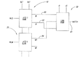
図1は本発明に基づくCAMセルを形成している第一メモリ回路10、第二メモリ回路20、比較回路30を示している。第一及び第二メモリ回路10,20は、夫々、データ値及びマスク値を格納するために使用される。マスク値は、比較回路30へ供給されるイネーブル又はディスエーブル信号である。比較回路30は、図1に示したように、第一メモリ回路10における格納されているデータ値を入力データ信号cf及びctに対して比較するために使用される。第二メモリ回路20がイネーブル値を格納した場合に、真マスク信号は比較回路30をイネーブルさせて比較を行うことを可能とさせ、且つディスエーブル値が格納された場合には、真マスク信号は比較回路30をディスエーブルさせ、従って比較が行われることはない。マッチ(一致)線は比較結果の出力を与える。比較回路がイネーブルされ且つ格納されているデータと比較データとの間にマッチ即ち一致が存在する場合には、マッチ線状態は同一状態に止まり、即ち高又は低に止まる。比較回路がイネーブルされ且つマッチ即ち一致が存在しない場合には、マッチ線の状態は変化され、高から低へ移行する。マッチ線へ接続されている多数のうちのいずれか1つのCAMセルがマッチ即ち一致でない場合には、その線は低へ移行される。比較セルに対してPチャンネルトランジスタが使用されている場合には、該線は高から低へ遷移する。信号線80はデータ真信号に対して第一メモリ回路10から比較回路30への相互接続を与える。信号線82はデータ偽信号に対してメモリ回路10から比較回路30への相互接続を与える。マッチ真データは信号線84を介して第二メモリ回路20から比較回路30ヘ供給され、且つマッチ偽データは第二メモリ回路20から出力されることはない。何故ならば、この特定の実施例においては、比較回路30においてマッチ偽信号を使用するものではないからである。別の構成においては、マッチ偽信号を使用することが可能であるが、選択した特定の構成においては、比較回路30は第二メモリ回路20からのマッチ真出力の信号値のみに基づいてセルのイネーブル又はディスエーブル動作を可能とすべく構成されており、従ってマッチ偽出力は必要ではない。
【0018】
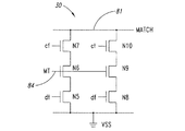
図2は図1の比較回路30の1実施例である。図2の実施例においては、図1の比較回路30の比較機能を与えるために6個のトランジスタN5−N10が使用されている。この実施例においては、図示したように、該トランジスタの全てはNチャンネルトランジスタであり、且つ以下の説明においては、Nチャンネルトランジスタが比較回路において使用されていることを仮定する。別の実施例ではその他のタイプのトランジスタを使用することが可能である。例えば、該トランジスタの幾つか又は全てに対してPチャンネルトランジスタを使用することが可能であり、且つこれらのPチャンネルトランジスタ及び接地及びパワー即ち電源への夫々の接続に対して適宜の信号レベルを逆にするものであるが、そのことは当業者にとって容易なことである。
【0019】
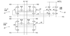
図3の実施例において、マッチ真信号線84がディスエーブル及びイネーブル機能を与えるために2個のトランジスタN6及びN9に対して与えられている。線84上のマッチ真信号が高であると、比較回路30がイネーブルされ、トランジスタN6及びN9の両方がターンオンして比較を行うことを可能とする。一方、線84上の信号が低である場合には、トランジスタN6及びN9がディスエーブルされ、従って格納されているデータと比較データとの間の比較を行うことは不可能である。この特定の実施例においては、マッチディスエーブルトランジスタが夫々の比較トランジスタとデータトランジスタとの間に位置されており、マッチ線と接地線との間に2つの別個の直列遅延を与えており、その両方は夫々のマッチディスエーブルトランジスタを有している。この特定のトランジスタ構造は、マッチデータ信号線から接地への完全に独立し且つ個別化した経路を与えている。好適実施例によれば、図3の概略図は図3−5に関して以下に説明するようにシリコンにおいてレイアウトしたものである。
【0020】
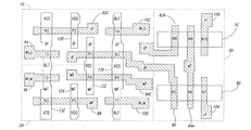
図4は図1のCAMセルの詳細な電気的概略図を示しており、図3の比較回路の実施例を使用している。
【0021】
図3に示したように、トランジスタN5乃至N10の符号も図4及び5に示してあり、且つ参照の便宜上夫々のトランジスタのゲート領域上に配置させており、勿論、該トランジスタはソース領域とドレイン領域とを有している。図3に示したように、第一及び第二メモリ回路10及び20のトランジスタN1−N4,P1−P4,T1−T4に対する符号は図4及び5においても示してあり、且つ便宜上夫々のトランジスタのゲート領域上に配置させているが、ソース領域とドレイン領域とを有している。
【0022】
全体的なCAMセルの1実施例を概略的に図3に示してある。第一メモリ回路10はデータ値を格納するデータセルである。第二メモリ回路20はマスク値を格納するマスクセルである。第一メモリ回路10はトランジスタP1,N1,T4,T3,N2,P2を有している。第二メモリセル20はトランジスタN4,P4,T1,T2,N3,P3を有している。比較回路30はトランジスタN5−N10を有している。
【0023】
図3に示したように、第一メモリ回路10はデータ値を格納するために使用され、従ってデータ回路として記されている。格納されているデータ値は比較回路30によって入力データ値と比較される。第一メモリ回路10はスタンダードの6トランジスタで完全なCMOSSRAMセルとして電気的に接続されている。それは以下の構成を有している。第一メモリ回路10の第二プルダウントランジスタN2のゲートは第二プルアップトランジスタP2のゲートと、第一プルダウントランジスタN1のドレイン領域と、第一プルアップトランジスタP1のドレイン領域と、第一パストランジスタT4のドレイン領域と、比較回路30のデータ偽トランジスタN8のゲートとに電気的に結合されており、それによりデータ偽dfノード82を画定している。第一メモリ回路10の第一プルダウントランジスタN1のゲートは、第一プルアップトランジスタP1のゲートと、第二プルダウントランジスタN2のドレイン領域と、第二プルアップトランジスタP2のドレイン領域と、第二パストランジスタT3のドレイン領域と、比較回路30のデータ真トランジスタN5のゲートとに電気的に結合されており、それによりデータ真dtノード80を画定している。第一メモリ回路10の第一パストランジスタT4は第一ワード線信号WLDへ電気的に結合しているゲートと、偽ビット線信号BLFへ電気的に結合しているソース領域とを有している。第一メモリ回路10の第二パストランジスタT3は、第一ワード線信号WLDへ電気的に結合しているゲートと真ビット線信号BLTへ電気的に結合しているソース領域とを有している。
【0024】
図3に示したように、第二メモリ回路20はマスク値MTを格納するために使用されており、従って、マスク回路として記してある。ノード84のマスク値MTは比較回路30をイネーブル又はディスエーブルさせる。第二メモリ回路20もスタンダードの6トランジスタの完全なCMOSSRAMセルである。それは以下の構成を有している。第二メモリ回路20の第二プルダウントランジスタN3のゲートは、第二プルアップトランジスタP3のゲートと、第一プルダウントランジスタN4のドレイン領域と、第一プルアップトランジスタP4のドレイン領域と、第一パストランジスタT1のドレイン領域とに電気的に結合しており、それによりマスク偽MFノードを画定している。第二メモリ回路20の第一プルダウントランジスタN4のゲートは、第一プルアップトランジスタP4のゲートと、第二プルダウントランジスタN3のドレイン領域と、第二プルアップトランジスタP3のドレイン領域と、第二パストランジスタT2のドレイン領域と、比較回路30の第一及び第二イネーブルトランジスタN6及びN9のゲートとに電気的に結合しており、それによりマスク真MTノード84を画定している。第二メモリ回路20の第一パストランジスタT1は、第二ワード線信号WLMへ電気的に結合されるゲートと、偽ビット線信号BLFへ電気的に結合されるソース領域とを有している。第二メモリ回路20の第二パストランジスタT2は、第二ワード線信号WLMへ電気的に結合されるゲートと、真ビット線信号BLTへ電気的に結合されるソース領域とを有している。
【0025】
上述した実施例において、メモリ回路10及び20は、両方共、6トランジスタ型のSRAMメモリ回路である。別の実施例においては、それらは4トランジスタ型のSRAMメモリ回路である。従って、図3に示した夫々の6トランジスタセルの各々の代わりに、負荷装置として2つのポリシリコン負荷抵抗を使用する4トランジスタメモリ回路を使用することが可能である。更に別の実施例においては、メモリ回路10及び20の各々は別の許容可能なメモリ回路から構成されている。例えば、それらは、EEPROM、EPROM、ROM、フラッシュメモリ回路、又はその他の許容可能な揮発性又は非揮発性のメモリ回路から構成することが可能である。その他のタイプのデータ格納又は編成を使用することが可能であり、例えばDRAM、吹き飛ばしたヒューズ、プログラムした即ち書込をしたROM、又はメモリ回路10及び20に対してその他の許容可能な格納装置等がある。従って、図1に示した夫々のメモリ回路10及び20の出力は、図1に示したように、且つ、夫々のセルの各々における特定のメモリの特定のタイプ、配置又は構成に拘わらずに、比較回路30へ供給される。
【0026】
図3に示したように、比較回路30は、第一メモリ回路10における相互接続80の信号dt及び相互接続82の信号dfによって供給される格納されているデータ値を信号cf及びctの入力データ値と比較するために使用される。好適実施例においては、比較回路30はN型トランジスタN5−N10からなる2つの並列スタック(積層体)として構成される。比較偽トランジスタN7は入力信号cfへ電気的に結合したゲートと、第一イネーブルトランジスタN6のドレイン領域へ電気的に結合しているソース領域と、MATCH(マッチ)信号へ電気的に結合しているドレイン領域とを有している。比較真トランジスタN10は、入力信号ctへ電気的に結合されるゲートと、第二イネーブルトランジスタN9のドレイン領域へ電気的に結合されるソース領域と、MATCH信号へ電気的に結合されるドレイン領域とを有している。第一イネーブルトランジスタN6は、データ真トランジスタN5のドレイン領域へ電気的に結合されるソース領域を有している。第二イネーブルトランジスタN9はデータ偽トランジスタN8のドレイン領域へ電気的に結合されるソース領域を有している。比較回路のトランジスタのこの構成は、CAMセルの基板面積の使用を減少させる利点を有している。
【0027】
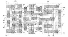
図4及び5に示したように、CAMセルはコンパクトな配置でシリコン内にレイアウトさせることが可能である。第一メモリ回路10、第二メモリ回路20、比較回路30はそれらがシリコン内にレイアウトされた状態で示されている。これらの図において、活性区域は黒い輪郭で示しており、ポリシリコンはハッチングで示してあり、金属1は点画で示してあり、コンタクトは四角の中にXで示してある。比較回路30は第一活性領域92と第二活性領域90とを有している。好適実施例においては、活性領域90及び92の両方はN導電型である。第一活性領域92は比較真トランジスタN10、第一イネーブルトランジスタN9、データ偽トランジスタN8の夫々のゲートの下側に形成されている。第一活性領域92はトランジスタN10のドレイン領域においてMATCH信号へ電気的に接続している。第一活性領域は、図5に示したように、データ偽トランジスタN8のソース領域における第一供給源VSSへ電気的に接続している。第二活性領域90は、比較偽トランジスタN7、第二イネーブルトランジスタN6、データ真トランジスタN5の夫々のゲートの下側に形成されている。第二活性領域90はトランジスタN7のドレイン領域においてMATCH信号へ電気的に接続している。第二活性領域90は、図5に示したように、データ真トランジスタN5のソース領域において第一供給源VSSへ電気的に接続している。第一及び第二活性領域92及び90の構成は、CAMセルの基板面積の使用を減少させる利点を有している。別の実施例においては、第一及び第二活性領域92及び90はP導電型である。図4及び5に示したように、本発明の1実施例においては、第一メモリ回路の活性領域はP導電型領域120,122及びN導電型領域132,130である。更に、第二メモリ回路の活性領域はP導電型領域124,122及びN導電型領域132,130である。
【0028】
図5に示したように、第一供給源VSSは、第一メモリ回路10の第一及び第二プルダウントランジスタN1及びN2のソース領域と、第二メモリ回路20の第一及び第二プルダウントランジスタN4及びN3のソース領域と、データ真トランジスタN5のソース領域と、データ偽トランジスタN8のソース領域とに電気的に接続している。第二供給源VDDは、第一メモリ回路10の第一及び第二プルアップトランジスタP1及びP2のソース領域と、第二メモリ回路20の第一及び第二プルアップトランジスタP4及びP3のソース領域とに電気的に接続している。第一及び第二メモリ回路10及び20から比較回路30への相互接続80,82,84は、ポリシリコンゲート物質、導電性物質、又は両方の物質の組合わせから形成されている領域によって達成されている。例えば、該導電性物質は、例えばアルミニウム、銅等の金属又は第二層ポリシリコン領域とすることが可能である。この相互接続の利点は、CAMセルの面積使用効率を減少させることである。
【0029】
図4に示したように、第一メモリ回路10と比較回路30との間の局所的相互接続80は、ポリシリコンの単一ストリップから構成されており、それは第一メモリ回路10の第一プルダウントランジスタN1のゲートと、第一メモリ回路10の第一プルアップトランジスタP1のゲートと、比較回路30のデータ真トランジスタN5のゲートとを形成している。1実施例においては、この局所的相互接続は図4及び5に示したように、ポリシリコンからなる領域80である。ポリシリコン領域80は、データ真ノードdtの一部である。該ゲートを形成するのと同一の導電性ストリップは相互接続ストリップでもあり、従ってそのストリップ全体は所定の物質からなる単一の共通の連続した層である。
【0030】
図4に示したように、局所的相互接続84Aが比較回路30の第一及び第二イネーブルトランジスタN6及びN9のゲート間に形成されており、それも単一の連続した所定の物質からなる層であり、従ってかなりの節約を提供している。局所的相互接続84Cが第二メモリ回路20の第一プルアップトランジスタP4と第一プルダウントランジスタN4のゲートの間に形成されておりそれも単一の連続した所定の物質からなる層であり、従ってかなりの節約を与えている。局所的相互接続84Bは、図5に示したように、相互接続84A乃至84Cを電気的に結合している。1実施例においては、ノードMTは図4及び5に示したように、局所的相互接続84A,84B,84Cを有する多層相互接続から形成されている。好適実施例においては、局所的相互接続84Aはポリシリコン領域を有しており、局所的相互接続84Bはアルミニウム又は第二層ポリシリコン領域等の導電性物質を有しており、且つ局所的相互接続84Cはポリシリコン領域を有している。
【0031】
図4に示したように、局所的相互接続82Cは第二プルダウントランジスタN2のゲートと第二プルアップトランジスタP2のゲートとを形成している。局所的相互接続82Aは比較回路30のデータ偽トランジスタN8のゲートを形成している。図5に示したように、局所的相互接続82Bは局所的相互接続82Cを相互接続82Aへ電気的に結合している。好適実施例においては、局所的相互接続82A,82B,82Cは多層相互接続としてデータ偽ノードdfを形成している。該多層相互接続は、金属82Bの領域と、ポリシリコン82Aの領域と、ポリシリコン82Cの領域とを図5に示したように有している。
【0032】
本発明の1実施例によれば、第一メモリ回路10のワード線は、図4に示されるように、メモリ回路内においてセグメント化されている。ワード線は、2つの部分、即ち第一部分94と第二部分102とを有している。これらのワード線部分は、ポリシリコンゲート物質から構成されており、且つ互いに物理的に別個であり且つ離隔している。それらは、勿論、ポリシリコンのブランク層の付着によって同一の層内に形成され、それが、次いで、パターン形成され且つエッチングされて当該技術において公知の処理技術を使用して同時的に全てのポリシリコンゲートを形成する。通常、従来のSRAMメモリ回路はメモリ回路内に2つのイネーブルトランジスタT3及びT4に対するゲート電極を形成するためにポリシリコンの切断されていない単一の連続したストリップを使用する。図4の実施例は、2つのイネーブルトランジスタに対する夫々のゲートを形成するためにポリシリコンの2つの別々の部分を使用することによりこのような従来のレイアウトとは異なるものである。本発明のレイアウトにおいて、このことは、通常より効率的な空間の使用であると仮定されているものを上回る空間節約の利点である。付加的な空間節約技術が図4の実施例のレイアウトにおいて実施されている。即ち、比較回路内のトランジスタP1,N1乃至N5を介してのデータ真からのデータノード接続及びデータ電極に対して使用されているポリシリコンの単一の連続的なストリップと共に、Pチャンネル及びNチャンネルトランジスタN2及びP2に対してポリシリコンからなる単一のストリップが使用されている。従って、2つのトランジスタP1及びN1に対してポリシリコンからなる単一の連続した部分が使用されている。同様に、第二メモリ回路もマスク真相互接続に対して及びゲート電極P4及びN4に対してポリシリコンの連続した部分84Cを使用している。連続したポリシリコンの単一の部分がゲート電極N3,P3及びマスク偽接続98に対して使用されている。ゲート電極T1及びT2に対してもポリシリコンからなる別個のストリップが使用されている。ポリシリコンからなる単一の連続したストリップが、マスク真接続84Aの共通ノードを形成する比較回路N9及びN6内の2個のイネーブルトランジスタに対して使用されている。更に、共通接続されるべき夫々のノードの各々は互いに電気的接続を行うことを容易とし、近付け且つ稠密とさせるために、互いに物理的に隣接して配設されている。例えば、データ偽dfに対する電気的接続の各々は互いに近接して大略真っ直ぐな水平線内に配設されており、従って単一の金属層82Bは図5に示したようにそれらを電気的に接続させるために容易に取付けることが可能である。
【0033】
同様に、データ真ノードdtの各々は互いに近接して電気的に接続され、従って金属80Bからなる単一のストリップはそれらを容易に電気的に接続することが可能である。マスクセル20におけるノードも同様に互いに近接して配設されている。例えば、マスクセル内部の全てのノードMTは互いに近接して配設されており、従って単一の金属層84Bはノードの全てを容易に電気的に接続することが可能である。ノードMFの全ても、図4及び5に示されるように、互いに隣接して配設されており、従って単一の金属層83が小さな大きさの空間内においてそれら全てを接続することが可能である。従って、比較回路と関連して、第一及び第二メモリ回路のレイアウトは、非常に小さな量のシリコン基板を使用し且つ密度が高いコンパクトなレイアウトを提供すべく構成されている。別の実施例においては、勿論、各メモリ回路のワード線は異なって配設することが可能であり、ワード線はポリシリコンの共通の連続したストリップから構成されており、メモリ回路内のその他のワード線又は相互接続も同様にすることが可能である。従って、これらの変形実施例は図示例のものと幾分異なったレイアウトを取ることが可能である。
【0034】
CAMセルの動作は、図4のMATCH(マッチ)線上において論理状態のマッチ(論理高)及び非マッチ(論理低)を与える。これらの論理状態は、入力データ信号cf及びctをメモリデータ信号dt及びdfに対して比較することにより発生される。入力データ信号cf及びctは公知の態様で比較回路30へ提供する前に補元が取られる。イネーブル信号MTは比較回路30のステータスを決定し、有効又は無効MATCH信号を発生する。初期的に、MATCH信号は高に設定される。MATCHが高である場合には、第一メモリ回路10の格納されているデータと入力データとの間の有効なマッチ即ち一致が示される。
【0035】
CAMセルの1実施例において、本装置の動作は以下のステップを有している。データ値を第一メモリ回路10内に格納する。マスク値を第二メモリ回路20内に格納する。比較データを比較回路30へ供給する。MATCH信号のステータスが同一のままであるか又は状態を変化するかについてモニタする。
【0036】
データ値の格納は、第一ワード線WLDへ高信号を印加し、ビット線真BLTへ第一値を印加し、且つ第二ビット線BLFへ第二値を印加することにより実施され、それにより第一メモリ回路10内に値を格納し且つ、図4に示したように、比較回路30へ印加されるデータ真信号dtの値を設定する。マスク値の格納は、第二ワード線WLMへ値を印加し、ビット線BLTへ値を印加し、第二ビット線BLFへ第二値を印加することを包含しており、それにより第二メモリ回路20内にマスク値を格納し、それにより比較回路30のトランジスタN6及びN9をイネーブルさせるイネーブル信号MTの値を設定する。ある時間において、比較トランジスタの入力信号ct及びcfに対して値を印加するステップが実施され、それにより第一メモリ回路10の格納されているデータ値dt及びdfを印加された入力信号値ct及びcfと比較する。比較が所望される場合には、ct及びcfは反対の値を有しているが、列上でグローバルブロックを実施することが所望される場合には、両方が低である場合がある。両方が低である場合には、比較が行われることはなく且つ全体的なセルグループがブロックされ、そのことは同一のct及びcf信号を受取る。MATCH信号線のステータスを検知することによりマッチ即ち一致が判別される。
【0037】
本明細書においてMOSトランジスタに関して使用されたドレイン及びソースの用語は、MOSトランジスタのチャンネルの両側における2つの領域を2つの別個の領域である一般的な意味で使用している。1つの領域が実際にドレイン又はソースであるとして識別することは、トランジスタの動作特性及び電気的接続、及び異なるノードに存在する電圧に依存して変化する場合がある。従って、本明細書全体及び特許請求の範囲において、ドレイン及びソースという用語は、その状態及び夫々のノードの値に依存して特定のトランジスタに対して互いに交換可能なものである。従って、これらの用語の各々はトランジスタの活性領域を意味することとして広義に理解すべきであり、且つ特定のトランジスタの動作状態に基づいてドレイン又はソースのいずれかであることを意味するものとして理解すべきである。
【0038】
以上、本発明の具体的実施の態様について詳細に説明したが、本発明は、これら具体例にのみ制限されるべきものではなく、本発明の技術的範囲を逸脱することなしに種々の変形が可能であることは勿論である。
【図面の簡単な説明】
【図1】 本発明の1実施例に基づくCAMセルの第一及び第二メモリ回路及び比較回路を示した概略図。
【図2】 図1のCAMセルの比較回路の1実施例を示した概略図。
【図3】 本発明に基づくCAMセルのトランジスタ概略接続の1実施例を示した概略図。
【図4】 1実施例に基づく活性領域及びポリシリコンを例示したCAMセルのシリコンにおけるレイアウトを示した概略平面図。
【図5】 活性金属及びコンタクトを示したCAMセルの付加的な層を示した図5のシリコン内のレイアウトの概略平面図。
【符号の説明】
10 第一メモリ回路
20 第二メモリ回路
30 比較回路
80,82 信号線
90 第二活性領域
92 第一活性領域[0001]
BACKGROUND OF THE INVENTION
The present invention relates to content-accessible memory (CAM) cells, and more particularly to structures and methods that improve the utilization of the area of a semiconductor substrate in a CAM cell.
[0002]
[Prior art]
In the communications industry, it is often necessary to determine the association between a first data element and a second data element. In order to satisfy this need, a content referenceable memory (CAM), also referred to as an associative memory device, is used to compare the input data value with the data value stored in the CAM cell. For example, the input data value may be a packet header that contains the address of one computer in a network of computers. The stored data value may be all addresses of computers in the network. The CAM cell array contained in the network router determines whether there is a relationship between the address in the packet header and the address of the computer in the network. In determining this relationship, a search and comparison method must be performed between the address in the packet header and all addresses in the network. This search and compare method is intensive both in terms of time and resources using conventional solutions consisting of RAM, CPU, software algorithms. Furthermore, for large input data words, eg 32 and 64 bits, the search and comparison method using conventional solutions is less efficient than the CAM cell array. Content-accessible memory provides a solution for fast search and compare operations.
[0003]
Usually, the CAM cell is composed of a first memory circuit, a second memory circuit, and a comparison circuit. The CAM array is composed of individual CAM cells. Each CAM cell receives one bit of the input data word. This bit is compared with the data stored in the first memory circuit of the CAM cell. The second memory circuit of the CAM cell stores the enable value. This enable value is used to enable or disable CAM cells in the CAM array during the data comparison period, which is used to compare a portion of the input data word during the sequence match phase. And enable another portion for comparison.
[0004]
In order to increase performance and achieve improved packing density, it is desirable to reduce the semiconductor substrate area used by the CAM cell. This reduction in substrate area is determined by the placement, organization and interconnection of the CAM cell transistors.
[0005]
[Problems to be solved by the invention]
The present invention has been made in view of the above points, and an object of the present invention is to provide an improved content-accessible memory (CAM) circuit that solves the above-described drawbacks of the prior art. Another object of the present invention is to provide an arrangement and method that improves the use of the area of a semiconductor substrate in a CAM cell.
[0006]
[Means for Solving the Problems]
According to one embodiment of the present invention, a CAM cell having a first memory circuit, a second memory circuit, and a comparison circuit is provided. The first memory circuit has a 6-transistor SRAM cell. The second memory circuit has a 6-transistor SRAM cell. Of course, the memory circuit can be any acceptable memory circuit including flip-flops, EEPROM memory cells, cross-coupled inverters, NOR gates, or any other acceptable memory circuit. The memory circuit, in one embodiment, is of a six-transistor structure organized in two parallel stacks of three transistors. On the other hand, it is possible to use a comparison circuit having a five-transistor structure, in which case it has two parallel stacks, each containing two transistors and one common fifth transistor. Yes.
[0007]
The first memory circuit is coupled to the first word line, the first bit line, and the second bit line. The first memory circuit stores data values for comparison with input data bits. The first memory circuit provides a data true signal and a data false signal to the comparison circuit, where these data signals are compared against the first and second input data signals cf and ct. The second memory circuit is connected to the second word line, the first bit line, and the second bit line. The second memory circuit stores the mask data value. The second memory circuit provides a mask true signal to the comparison circuit to enable or disable the comparison circuit.
[0008]
According to one embodiment of the present invention, the interconnection of the transistors of the first and second memory circuits to the transistors of the comparison circuit is comprised of a region made of a conductive material.
[0009]
According to a first embodiment, the conductive material is polysilicon. In another embodiment, the conductive material is a metal layer and may be any acceptable metal including aluminum, copper, tungsten, titanium polysilicide, or various combinations or alloys thereof. Is possible. Of course, the type of conductivity used can be changed in the cell from polysilicon to metal by appropriate contacts, vias and interconnects to provide a conductive path from the memory circuit to the appropriate node in the comparator circuit. Is possible.
[0010]
One embodiment of the present invention provides a method of operating a CAM cell, the method comprising storing data in the CAM cell and applying a signal to an enable line of the device, in which case the enable The line is a shared gate structure and thereby enabling the device, applying the input data, comparing the input data with the first data, and outputting a status change on the match signal line And a step of performing.
[0011]
An embodiment of the present invention provides a method of operating a CAM cell, wherein the storing step further stores data in a first memory circuit and an enable value in a second memory circuit. Is stored. To store data in the first memory circuit, a value is applied to the first word line, the data is applied to the first bit line, the complement of the data is applied to the second bit line, and A data value is stored in the first memory circuit. The enable value is stored in the second memory circuit in a similar manner and used to set the enable or disable terminal in the comparison circuit.
[0012]
In one embodiment of the invention, a content-accessible memory is formed in an integrated circuit that has the use of improved semiconductor substrate area.
[0013]
One embodiment of the present invention provides an improvement to the utilization of integrated circuit area by reducing the layout area of the CAM cell and thus reducing manufacturing costs. Embodiments of the present invention are applicable to binary and ternary CAM cells as well as 4-state CAM cells.
[0014]
One advantage of the present invention is that, given a large data input word, the CAM cell is fast to make a match determination.
[0015]
One advantage of the present invention is a CAM cell with an improved organization of transistors that reduces the substrate area of the CAM cell and array.
[0016]
One advantage of the present invention is a CAM cell with improved interconnection of transistors that are small in size relative to the CAM cell and array.
[0017]
DETAILED DESCRIPTION OF THE INVENTION
FIG. 1 shows a
[0018]
FIG. 2 shows an embodiment of the
[0019]
In the embodiment of FIG. 3, a match
[0020]
FIG. 4 shows a detailed electrical schematic of the CAM cell of FIG. 1, using the embodiment of the comparison circuit of FIG.
[0021]
As shown in FIG. 3, the reference numerals of the transistors N5 to N10 are also shown in FIGS. 4 and 5 and are arranged on the gate regions of the respective transistors for convenience of reference. And have a region. As shown in FIG. 3, the symbols for the transistors N1-N4, P1-P4, T1-T4 of the first and
[0022]
One embodiment of the overall CAM cell is shown schematically in FIG. The
[0023]
As shown in FIG. 3, the
[0024]
As shown in FIG. 3, the
[0025]
In the embodiment described above, the
[0026]
As shown in FIG. 3, the
[0027]
As shown in FIGS. 4 and 5, CAM cells can be laid out in silicon in a compact arrangement. The
[0028]
Figure 5 As shown in FIG. 1, the first supply source VSS includes the source regions of the first and second pull-down transistors N1 and N2 of the
[0029]
As shown in FIG. 4, the
[0030]
As shown in FIG. 4, a
[0031]
As shown in FIG. 4,
[0032]
According to one embodiment of the present invention, the word lines of the
[0033]
Similarly, each of the data true nodes dt are electrically connected in close proximity to each other so that a single strip of metal 80B can easily connect them electrically. Similarly, the nodes in the
[0034]
The operation of the CAM cell provides a logic state match (logic high) and non-match (logic low) on the MATCH (match) line of FIG. These logic states are generated by comparing the input data signals cf and ct against the memory data signals dt and df. The input data signals cf and ct are complemented before being provided to the
[0035]
In one embodiment of the CAM cell, the operation of the apparatus has the following steps. The data value is stored in the
[0036]
The data value is stored by applying a high signal to the first word line WLD, applying a first value to the bit line true BLT, and applying a second value to the second bit line BLF, thereby The value is stored in the
[0037]
The drain and source terms used herein with respect to a MOS transistor use the two regions on either side of the channel of the MOS transistor in the general sense of two separate regions. The identification of a region as actually drain or source may vary depending on the operating characteristics and electrical connections of the transistor and the voltage present at the different nodes. Accordingly, throughout the specification and claims, the terms drain and source are interchangeable for a particular transistor depending on its state and the value of the respective node. Thus, each of these terms should be broadly understood as meaning the active region of a transistor, and understood as meaning either drain or source based on the particular transistor operating state. Should.
[0038]
Although specific embodiments of the present invention have been described in detail above, the present invention should not be limited to these specific examples, and various modifications can be made without departing from the technical scope of the present invention. Of course, it is possible.
[Brief description of the drawings]
FIG. 1 is a schematic diagram illustrating first and second memory circuits and a comparison circuit of a CAM cell according to an embodiment of the present invention.
FIG. 2 is a schematic diagram showing one embodiment of a comparison circuit of the CAM cell in FIG. 1;
FIG. 3 is a schematic diagram showing one embodiment of transistor schematic connection of a CAM cell according to the present invention.
FIG. 4 is a schematic plan view showing a layout in silicon of a CAM cell illustrating an active region and polysilicon according to one embodiment.
5 is a schematic plan view of the layout in silicon of FIG. 5 showing additional layers of the CAM cell showing active metal and contacts.
[Explanation of symbols]
10 First memory circuit
20 Second memory circuit
30 Comparison circuit
80,82 signal lines
90 Second active region
92 First active region
Claims (21)
第一値に設定されている論理状態を有するマッチ信号出力、
イネーブル入力と、前記マッチ信号出力へ結合しているマッチ出力と、比較データ信号へ結合している比較データ入力と、格納データ入力とを具備しており格納データ値を比較データ値と比較する比較回路であって、前記イネーブル入力がイネーブル真信号を受取り且つ前記格納データ入力が格納データ信号を受取り且つ前記比較データ入力が比較データ信号を受取る場合には、前記マッチ信号出力の論理状態が第二値ヘ変化しそれによりマッチ無しを表わす比較回路、
第一及び第二ワード線と、第一及び第二ビット線と、格納データ出力と、前記格納データ出力を前記比較回路の格納データ入力へ電気的に結合させる第一導電性ストリップとを具備しておりデータ値を格納する第一データ格納装置であって、前記格納データ出力が前記格納データ信号を供給する第一データ格納装置、
第三及び第四ワード線と、第一及び第二ビット線と、イネーブル出力と、前記イネーブル出力を前記比較回路のイネーブル入力へ電気的に結合させる第二導電性ストリップとを具備しておりイネーブル値を格納する第二データ格納装置であって、前記イネーブル出力が前記イネーブル真信号を供給する第二データ格納装置、
を有しており、前記第一データ格納装置は前記半導体基板の第一領域内に配置されている第一複数個のトランジスタを有しており、前記第二データ格納装置は前記半導体基板の前記第一領域に隣接している第二領域内に配置されている第二複数個のトランジスタを有しており、且つ前記比較回路は前記半導体基板の前記第一及び第二領域に隣接している第三領域内に配置されている第三複数個のトランジスタを有しており、前記第三領域内には各々が複数個の第一導電型のソース・ドレイン領域を含む第一及び第二活性領域が設けられており、前記第三複数個のトランジスタの半分が前記第一活性領域に配置されて一対の隣接するトランジスタ間において1個のソース・ドレイン領域を共有しており且つ前記第三複数個のトランジスタの残りの半分が前記第二活性領域に配置されて一対の隣接するトランジスタ間において1個のソース・ドレイン領域を共有していることを特徴とする内容参照可能メモリ回路。In a memory circuit capable of referring to contents in a semiconductor substrate,
A match signal output having a logic state set to a first value,
A comparison comprising an enable input, a match output coupled to the match signal output, a comparison data input coupled to a comparison data signal, and a storage data input for comparing the stored data value with the comparison data value A logic state of the match signal output when the enable input receives an enable true signal, the stored data input receives a stored data signal, and the comparison data input receives a comparison data signal; A comparison circuit which changes to a value and thereby represents no match,
First and second word lines; first and second bit lines; a stored data output; and a first conductive strip for electrically coupling the stored data output to a stored data input of the comparator circuit. A first data storage device for storing data values, wherein the stored data output provides the stored data signal;
An enable comprising third and fourth word lines, first and second bit lines, an enable output, and a second conductive strip for electrically coupling the enable output to an enable input of the comparator circuit. A second data storage device for storing a value, wherein the enable output provides the enable true signal;
The first data storage device includes a first plurality of transistors disposed in a first region of the semiconductor substrate, and the second data storage device includes the first data storage device of the semiconductor substrate. A second plurality of transistors disposed in a second region adjacent to the first region, and the comparison circuit is adjacent to the first and second regions of the semiconductor substrate; A third plurality of transistors disposed in the third region, each of the first and second active regions including a plurality of first-conductivity-type source / drain regions in the third region; A region is provided, half of the third plurality of transistors are disposed in the first active region, share one source / drain region between a pair of adjacent transistors, and the third plurality Rest of transistors Half the second active is arranged in the region by a pair of adjacent content addressable memory circuit, characterized in that they share a single source and drain regions between transistors.
第一及び第二メモリ回路が設けられており、各メモリ回路は第一及び第二プルダウントランジスタと、第一及び第二プルアップトランジスタと、第一及び第二パストランジスタとを具備しており、各トランジスタはゲートと、ソース領域と、ドレイン領域とを具備しており、
第一及び第二比較トランジスタと、第一及び第二イネーブルトランジスタと、データ真及びデータ偽トランジスタとを具備する比較回路が設けられており、各トランジスタはゲートと、ソース領域と、ドレイン領域とを具備しており、
前記第一メモリ回路の前記第一プルダウントランジスタのゲートは前記第一メモリ回路の前記第一プルアップトランジスタのゲート、前記第一メモリ回路の第二プルダウントランジスタのドレイン領域、前記第一メモリ回路の第二プルアップトランジスタのドレイン領域、前記第一メモリ回路の第二パストランジスタのドレイン領域、前記比較回路のデータ真トランジスタのゲートへ電気的に結合しており、
前記第一メモリ回路の第二プルダウントランジスタのゲートは、前記第一メモリ回路の第二プルアップトランジスタのゲート、前記第一メモリ回路の第一プルダウントランジスタのドレイン領域、前記第一メモリ回路の第一プルアップトランジスタのドレイン領域、前記第一メモリ回路の第一パストランジスタのドレイン領域、前記比較回路のデータ偽トランジスタのゲートへ電気的に結合しており、
前記第二メモリ回路の第二プルダウントランジスタのゲートは、前記第二メモリ回路の第二プルアップトランジスタのゲート、前記第二メモリ回路の第一プルダウントランジスタのドレイン領域、前記第二メモリ回路の第一プルアップトランジスタのドレイン領域、前記第二メモリ回路の第一パストランジスタのドレイン領域へ電気的に結合しており、
前記第二メモリ回路の第一プルダウントランジスタのゲートは、前記第二メモリ回路の第一プルアップトランジスタのゲート、前記第二メモリ回路の第二プルダウントランジスタのドレイン領域、前記第二メモリ回路の第二プルアップトランジスタのドレイン領域、前記第二メモリ回路の第二パストランジスタのドレイン領域、前記比較回路の前記第一及び第二イネーブルトランジスタのゲートへ電気的に結合しており、
前記第一比較トランジスタは、そのゲートを第一比較信号へ電気的に結合し、そのソース領域を前記第一イネーブルトランジスタのドレイン領域へ電気的に結合し、そのドレイン領域をマッチ信号へ電気的に結合し、
前記第二比較トランジスタはそのゲートを第二比較信号へ電気的に結合し、そのソース領域を前記第二イネーブルトランジスタのドレイン領域へ電気的に結合し、そのドレイン領域を前記マッチ信号へ電気的に結合し、
前記第一イネーブルトランジスタはそのソース領域を前記データ真トランジスタのドレイン領域へ電気的に結合し、
前記第二イネーブルトランジスタはそのソース領域を前記データ偽トランジスタのドレイン領域へ電気的に結合し、
前記第一メモリ回路の第一パストランジスタはそのゲートを第一ワード線信号へ電気的に結合し、そのソース領域を第一ビット線信号へ電気的に結合し、
前記第一メモリ回路の第二パストランジスタはそのゲートを前記第一ワード線信号へ電気的に結合し、そのソース領域を第二ビット線信号へ電気的に結合し、
前記第二メモリ回路の第一パストランジスタはそのゲートを第二ワード線信号へ電気的に結合し、そのソース領域を前記第一ビット線信号へ電気的に結合し、
前記第二メモリ回路の第二パストランジスタはそのゲートを前記第二ワード線信号へ電気的に結合し、そのソース領域を前記第二ビット線信号へ電気的に結合し、
第一供給源が前記第一メモリ回路の第一及び第二プルダウントランジスタのソース領域、前記第二メモリ回路の第一及び第二プルダウントランジスタのソース領域、前記データ真トランジスタのソース領域、前記データ偽トランジスタのソース領域へ電気的に結合しており、
第二供給源が、前記第一メモリ回路の第一及び第二プルアップトランジスタのソース領域、前記第二メモリ回路の第一及び第二プルアップトランジスタのソース領域へ電気的に結合しており、
前記第一メモリ回路の前記第一及び第二プルアップトランジスタと前記第一及び第二プルダウントランジスタと前記第一及び第二パストランジスタとは前記半導体基板の第一領域内に配置されており、前記第二メモリ回路の前記第一及び第二プルアップトランジスタと前記第一及び第二プルダウントランジスタと前記第一及び第二パストランジスタとは前記半導体基板の前記第一領域に隣接している第二領域内に配置されており、且つ前記比較回路の前記第一及び第二比較トランジスタと前記第一及び第二イネーブルトランジスタと前記データ真及びデータ偽トランジスタとは前記半導体基板の前記第一及び第二領域に隣接している第三領域内に配置されており、
前記第一及び第二比較トランジスタの各ソース領域と前記第一及び第二イネーブルトランジスタの各ドレイン領域とはこれらにより共有されている第一導電型の同一の活性領域であり、且つ前記第一及び第二イネーブルトランジスタの各ソース領域と前記データ真及びデータ偽トランジスタの各ドレイン領域とはこれらにより共有されている第一導電型の同一の活性領域である、
ことを特徴とする内容参照可能メモリ回路。In a memory circuit capable of referring to contents in a semiconductor substrate,
First and second memory circuits are provided, each memory circuit comprising first and second pull-down transistors, first and second pull-up transistors, and first and second pass transistors, Each transistor has a gate, a source region, and a drain region,
A comparison circuit comprising a first and second comparison transistor, a first and second enable transistor, and a data true and data false transistor is provided, each transistor having a gate, a source region, and a drain region. Has
The gate of the first pull-down transistor of the first memory circuit is the gate of the first pull-up transistor of the first memory circuit, the drain region of the second pull-down transistor of the first memory circuit, the first of the first memory circuit Electrically coupled to the drain region of the two pull-up transistors, the drain region of the second pass transistor of the first memory circuit, and the gate of the data true transistor of the comparator circuit;
The gate of the second pull-down transistor of the first memory circuit is the gate of the second pull-up transistor of the first memory circuit, the drain region of the first pull-down transistor of the first memory circuit, the first of the first memory circuit Electrically coupled to the drain region of the pull-up transistor, the drain region of the first pass transistor of the first memory circuit, and the gate of the data pseudo transistor of the comparison circuit;
The gate of the second pull-down transistor of the second memory circuit is the gate of the second pull-up transistor of the second memory circuit, the drain region of the first pull-down transistor of the second memory circuit, and the first of the second memory circuit. Electrically coupled to the drain region of the pull-up transistor and the drain region of the first pass transistor of the second memory circuit;
The gate of the first pull-down transistor of the second memory circuit includes a gate of the first pull-up transistor of the second memory circuit, a drain region of the second pull-down transistor of the second memory circuit, and a second of the second memory circuit. Electrically coupled to the drain region of the pull-up transistor, the drain region of the second pass transistor of the second memory circuit, the gates of the first and second enable transistors of the comparator circuit;
The first comparison transistor has its gate electrically coupled to the first comparison signal, its source region electrically coupled to the drain region of the first enable transistor, and its drain region electrically coupled to the match signal. Combine and
The second comparison transistor electrically couples its gate to the second comparison signal, electrically couples its source region to the drain region of the second enable transistor, and electrically connects its drain region to the match signal. Combine and
The first enable transistor electrically couples its source region to the drain region of the data true transistor;
The second enable transistor electrically couples its source region to the drain region of the data pseudo-transistor;
A first pass transistor of the first memory circuit electrically couples its gate to a first word line signal and electrically couples its source region to a first bit line signal;
A second pass transistor of the first memory circuit electrically couples its gate to the first word line signal and electrically couples its source region to a second bit line signal;
A first pass transistor of the second memory circuit electrically couples its gate to a second word line signal and electrically couples its source region to the first bit line signal;
A second pass transistor of the second memory circuit electrically couples its gate to the second word line signal and electrically couples its source region to the second bit line signal;
The first supply source is the source region of the first and second pull-down transistors of the first memory circuit, the source region of the first and second pull-down transistors of the second memory circuit, the source region of the data true transistor, the data false Electrically coupled to the source region of the transistor,
A second source is electrically coupled to the source regions of the first and second pull-up transistors of the first memory circuit, the source regions of the first and second pull-up transistors of the second memory circuit;
The first and second pull-up transistors, the first and second pull-down transistors, and the first and second pass transistors of the first memory circuit are disposed in a first region of the semiconductor substrate, and The first and second pull-up transistors, the first and second pull-down transistors, and the first and second pass transistors of the second memory circuit are adjacent to the first region of the semiconductor substrate. The first and second comparison transistors, the first and second enable transistors, and the data true and data false transistors of the comparison circuit are arranged in the first and second regions of the semiconductor substrate. Is located in the third region adjacent to
The source regions of the first and second comparison transistors and the drain regions of the first and second enable transistors are the same active region of the first conductivity type shared by them, and the first and second transistors Each source region of the second enable transistor and each drain region of the data true and data false transistors are the same active region of the first conductivity type shared by them.
A content referenceable memory circuit characterized by the above.
Applications Claiming Priority (1)
| Application Number | Priority Date | Filing Date | Title |
|---|---|---|---|
| US10/163,848 US6678184B2 (en) | 2002-06-05 | 2002-06-05 | CAM cell having compare circuit formed over two active regions |
Publications (2)
| Publication Number | Publication Date |
|---|---|
| JP2004014102A JP2004014102A (en) | 2004-01-15 |
| JP4541663B2 true JP4541663B2 (en) | 2010-09-08 |
Family
ID=29549330
Family Applications (1)
| Application Number | Title | Priority Date | Filing Date |
|---|---|---|---|
| JP2003160965A Expired - Lifetime JP4541663B2 (en) | 2002-06-05 | 2003-06-05 | CAM cell |
Country Status (4)
| Country | Link |
|---|---|
| US (1) | US6678184B2 (en) |
| EP (1) | EP1369877B1 (en) |
| JP (1) | JP4541663B2 (en) |
| DE (1) | DE60333700D1 (en) |
Families Citing this family (13)
| Publication number | Priority date | Publication date | Assignee | Title |
|---|---|---|---|---|
| KR100435804B1 (en) * | 2002-06-28 | 2004-06-10 | 삼성전자주식회사 | Ternary content addressable memory device |
| US6900999B1 (en) * | 2003-06-30 | 2005-05-31 | Integrated Device Technology, Inc. | Ternary content addressable memory (TCAM) cells with small footprint size and efficient layout aspect ratio |
| US7315466B2 (en) | 2004-08-04 | 2008-01-01 | Samsung Electronics Co., Ltd. | Semiconductor memory device and method for arranging and manufacturing the same |
| US7233512B2 (en) | 2005-02-01 | 2007-06-19 | Stmicroelectronics, Inc. | Content addressable memory circuit with improved memory cell stability |
| US7218542B2 (en) * | 2005-05-23 | 2007-05-15 | Stmicroelectronics, Inc. | Physical priority encoder |
| FR2888387A1 (en) * | 2005-07-05 | 2007-01-12 | St Microelectronics Sa | Content addressable memory cell, has memory circuit with comparison circuit having NMOS transistors and isolation transistors, which are implanted in respective active zones, where all transistors are oriented vertically |
| US7196922B2 (en) * | 2005-07-25 | 2007-03-27 | Stmicroelectronics, Inc. | Programmable priority encoder |
| US7978561B2 (en) * | 2005-07-28 | 2011-07-12 | Samsung Electronics Co., Ltd. | Semiconductor memory devices having vertically-stacked transistors therein |
| US7170769B1 (en) * | 2005-10-03 | 2007-01-30 | Texas Instruments Incorporated | High performance and reduced area architecture for a fully parallel search of a TCAM cell |
| US8730704B1 (en) * | 2012-02-10 | 2014-05-20 | Netlogic Microsystems, Inc. | Content addressable memory array having local interconnects |
| KR102596601B1 (en) | 2016-12-26 | 2023-10-31 | 삼성전자주식회사 | Semiconductor device and method for fabricating the same |
| US10741585B2 (en) * | 2018-06-29 | 2020-08-11 | Sandisk Technologies Llc | Content addressable memory using threshold-adjustable vertical transistors and methods of forming the same |
| CN112837731B (en) * | 2020-12-31 | 2024-08-06 | 中国科学院上海微系统与信息技术研究所 | Static memory unit for memory multiplexing |
Family Cites Families (9)
| Publication number | Priority date | Publication date | Assignee | Title |
|---|---|---|---|---|
| JPH0421997A (en) * | 1990-05-16 | 1992-01-24 | Nec Corp | Content-addresable circuit |
| EP0500000B1 (en) * | 1991-02-12 | 1996-08-14 | Comadur S.A. | Mouse controller |
| US6044005A (en) * | 1999-02-03 | 2000-03-28 | Sibercore Technologies Incorporated | Content addressable memory storage device |
| US6108227A (en) * | 1999-07-23 | 2000-08-22 | Lara Technology, Inc. | Content addressable memory having binary and ternary modes of operation |
| US6154384A (en) * | 1999-11-12 | 2000-11-28 | Netlogic Microsystems, Inc. | Ternary content addressable memory cell |
| JP4357101B2 (en) * | 2000-08-23 | 2009-11-04 | 株式会社ルネサステクノロジ | Semiconductor memory device |
| US6400592B1 (en) * | 2000-09-09 | 2002-06-04 | Cadence Design Systems, Inc. | Content addressable memory cell and design methodology |
| US6373739B1 (en) * | 2000-12-06 | 2002-04-16 | Integrated Device Technology, Inc. | Quad CAM cell with minimum cell size |
| US6421265B1 (en) * | 2001-03-22 | 2002-07-16 | Integrated Devices Technology, Inc. | DRAM-based CAM cell using 3T or 4T DRAM cells |
-
2002
- 2002-06-05 US US10/163,848 patent/US6678184B2/en not_active Expired - Lifetime
-
2003
- 2003-06-05 EP EP03253553A patent/EP1369877B1/en not_active Expired - Lifetime
- 2003-06-05 DE DE60333700T patent/DE60333700D1/en not_active Expired - Lifetime
- 2003-06-05 JP JP2003160965A patent/JP4541663B2/en not_active Expired - Lifetime
Also Published As
| Publication number | Publication date |
|---|---|
| EP1369877A3 (en) | 2007-08-08 |
| US20030227787A1 (en) | 2003-12-11 |
| DE60333700D1 (en) | 2010-09-23 |
| US6678184B2 (en) | 2004-01-13 |
| EP1369877A2 (en) | 2003-12-10 |
| JP2004014102A (en) | 2004-01-15 |
| EP1369877B1 (en) | 2010-08-11 |
Similar Documents
| Publication | Publication Date | Title |
|---|---|---|
| US6480406B1 (en) | Content addressable memory cell | |
| JP4034101B2 (en) | Ternary contents referenceable memory half cell and ternary contents referenceable memory cell | |
| CN103377685B (en) | Device for sram cell | |
| JP4903338B2 (en) | Improved high density memory cell | |
| JP4541663B2 (en) | CAM cell | |
| US6822300B2 (en) | Semiconductor memory device | |
| TWI420536B (en) | Memory cell with improved read stability | |
| US7558095B2 (en) | Memory cell for content-addressable memory | |
| US20050146947A1 (en) | Semiconductor device | |
| US11798615B2 (en) | High density array, in memory computing | |
| Mohan et al. | Low-leakage storage cells for ternary content addressable memories | |
| US10910056B2 (en) | Semiconductor device | |
| Satti et al. | Hybrid self-controlled precharge-free CAM design for low power and high performance | |
| US6504788B1 (en) | Semiconductor memory with improved soft error resistance | |
| Mohan | Low-power high-performance ternary content addressable memory circuits | |
| JP2004515869A (en) | Associative memory cell and design method | |
| US6834003B2 (en) | Content addressable memory with PFET passgate SRAM cells | |
| US7233512B2 (en) | Content addressable memory circuit with improved memory cell stability | |
| US20150262667A1 (en) | Low power hit bitline driver for content-addressable memory | |
| US8730704B1 (en) | Content addressable memory array having local interconnects | |
| JP2009525561A (en) | Range matching cell and CAM using the same | |
| Nanoti et al. | Design of high speed addressable memory based on memory-resistance using 45nm CMOS technology | |
| Naresh et al. | Stacked Keeper with Body Bias Approach to Reduce Leakage Power for 2-Byte CAM Using 180NM CMOS Technology | |
| JP2002025274A (en) | SRAM cell and semiconductor integrated circuit incorporating the same | |
| Sullivan et al. | A 1.8 V, 2.0 ns cycle, 32 KB embedded memory with interleaved castout/reload |
Legal Events
| Date | Code | Title | Description |
|---|---|---|---|
| A621 | Written request for application examination |
Free format text: JAPANESE INTERMEDIATE CODE: A621 Effective date: 20060601 |
|
| A131 | Notification of reasons for refusal |
Free format text: JAPANESE INTERMEDIATE CODE: A131 Effective date: 20090428 |
|
| A601 | Written request for extension of time |
Free format text: JAPANESE INTERMEDIATE CODE: A601 Effective date: 20090728 |
|
| A602 | Written permission of extension of time |
Free format text: JAPANESE INTERMEDIATE CODE: A602 Effective date: 20090731 |
|
| A521 | Request for written amendment filed |
Free format text: JAPANESE INTERMEDIATE CODE: A523 Effective date: 20090827 |
|
| A131 | Notification of reasons for refusal |
Free format text: JAPANESE INTERMEDIATE CODE: A131 Effective date: 20100209 |
|
| A521 | Request for written amendment filed |
Free format text: JAPANESE INTERMEDIATE CODE: A523 Effective date: 20100428 |
|
| TRDD | Decision of grant or rejection written | ||
| A01 | Written decision to grant a patent or to grant a registration (utility model) |
Free format text: JAPANESE INTERMEDIATE CODE: A01 Effective date: 20100525 |
|
| A01 | Written decision to grant a patent or to grant a registration (utility model) |
Free format text: JAPANESE INTERMEDIATE CODE: A01 |
|
| A61 | First payment of annual fees (during grant procedure) |
Free format text: JAPANESE INTERMEDIATE CODE: A61 Effective date: 20100624 |
|
| R150 | Certificate of patent or registration of utility model |
Free format text: JAPANESE INTERMEDIATE CODE: R150 Ref document number: 4541663 Country of ref document: JP Free format text: JAPANESE INTERMEDIATE CODE: R150 |
|
| FPAY | Renewal fee payment (event date is renewal date of database) |
Free format text: PAYMENT UNTIL: 20130702 Year of fee payment: 3 |
|
| R250 | Receipt of annual fees |
Free format text: JAPANESE INTERMEDIATE CODE: R250 |
|
| R250 | Receipt of annual fees |
Free format text: JAPANESE INTERMEDIATE CODE: R250 |
|
| R250 | Receipt of annual fees |
Free format text: JAPANESE INTERMEDIATE CODE: R250 |
|
| R250 | Receipt of annual fees |
Free format text: JAPANESE INTERMEDIATE CODE: R250 |
|
| R250 | Receipt of annual fees |
Free format text: JAPANESE INTERMEDIATE CODE: R250 |
|
| R250 | Receipt of annual fees |
Free format text: JAPANESE INTERMEDIATE CODE: R250 |
|
| R250 | Receipt of annual fees |
Free format text: JAPANESE INTERMEDIATE CODE: R250 |
|
| R250 | Receipt of annual fees |
Free format text: JAPANESE INTERMEDIATE CODE: R250 |
|
| R250 | Receipt of annual fees |
Free format text: JAPANESE INTERMEDIATE CODE: R250 |
|
| R250 | Receipt of annual fees |
Free format text: JAPANESE INTERMEDIATE CODE: R250 |
|
| EXPY | Cancellation because of completion of term |