JP4536498B2 - Analog to digital converter - Google Patents
Analog to digital converter Download PDFInfo
- Publication number
- JP4536498B2 JP4536498B2 JP2004351249A JP2004351249A JP4536498B2 JP 4536498 B2 JP4536498 B2 JP 4536498B2 JP 2004351249 A JP2004351249 A JP 2004351249A JP 2004351249 A JP2004351249 A JP 2004351249A JP 4536498 B2 JP4536498 B2 JP 4536498B2
- Authority
- JP
- Japan
- Prior art keywords
- reference voltage
- reference voltages
- analog
- unit
- monitoring
- Prior art date
- Legal status (The legal status is an assumption and is not a legal conclusion. Google has not performed a legal analysis and makes no representation as to the accuracy of the status listed.)
- Expired - Fee Related
Links
Images
Landscapes
- Analogue/Digital Conversion (AREA)
Description
本発明は、アナログデジタル変換器に関し、特に2ステップフラッシュ型のアナログデジタル変換器に関する。 The present invention relates to an analog-digital converter, and more particularly to a two-step flash type analog-digital converter.
アナログ入力信号を量子化し、デジタル信号に変換するアナログデジタル変換器(以下、ADコンバータという)は、さまざまなデジタル信号処理回路の基本となる重要な回路ブロックのひとつである。特に通信機器である携帯電話や、オーディオ機器などの内部に使用されるDSP(Digital Signal Processor)においては、ADコンバータによって信号処理速度や信号処理の精度が決定される場合がある。 An analog-digital converter (hereinafter referred to as an AD converter) that quantizes an analog input signal and converts it into a digital signal is one of the important circuit blocks that form the basis of various digital signal processing circuits. In particular, in a DSP (Digital Signal Processor) used in a mobile phone or an audio device as a communication device, the signal processing speed and the accuracy of signal processing may be determined by an AD converter.
ADコンバータには、フラッシュ型や2ステップフラッシュ型、ΔΣ型のADコンバータなど、回路形式の異なるいくつかのバリエーションが存在する。
このなかで、2ステップフラッシュ型のADコンバータは、第1段階として、粗い精度で設定された複数の基準電圧を用いて上位ビットを判定し、第2段階として、その判定結果にもとづいて設定された複数の密な基準電圧を用いて下位ビットを判定することによりデジタル変換を行う(特許文献1参照)。この2ステップフラッシュ型のADコンバータは、上位ビットと下位ビットを分けて変換するため、すべてのビットを同時に比較するフラッシュ型と比較して、コンパレータの数が減らすことができ、回路規模を小さくすることができる。
There are several variations of the AD converter, such as a flash type, a two-step flash type, and a ΔΣ type AD converter.
Among them, the two-step flash AD converter determines the upper bits using a plurality of reference voltages set with coarse accuracy as the first stage, and is set based on the determination result as the second stage. The digital conversion is performed by determining the lower bits using a plurality of dense reference voltages (see Patent Document 1). Since this two-step flash AD converter converts upper bits and lower bits separately, the number of comparators can be reduced and the circuit scale can be reduced compared to the flash type that compares all bits simultaneously. be able to.
ここで、1段階目で上位2ビットを判定し、2段階目で下位2ビットを判定する4ビットの2ステップフラッシュ型のADコンバータを考える。このようなADコンバータでは、第1段階において、アナログ入力信号と、上位ビットの1LSB(Least Significant Bit)で量子化された量子化値4、8、12に対応する基準電圧とが比較される。その結果、アナログ入力信号が8〜12の範囲であると判定されると、つぎに、第2段階において、下位ビットの1LSBで量子化された量子化値8〜12の範囲に対応する基準電圧とアナログ入力信号との比較を行い、下位2ビットが決定される。
Consider a 4-bit 2-step flash AD converter that determines the upper 2 bits in the first stage and determines the lower 2 bits in the second stage. In such an AD converter, in a first stage, an analog input signal is compared with reference voltages corresponding to quantized
ところが、第1段階に用いられるコンパレータは、オフセットを有する場合があり、このオフセットによって上位ビットの判定に誤りが生ずる場合がある。たとえば、実際のアナログ入力信号が量子化値7に相当する信号であるにもかかわらず、第1段階における上位ビットの判定に誤りが発生し、8〜12の範囲であると判定された場合、第2段階において、量子化値8〜12に対応する基準電圧と比較したのでは1LSB分の誤差が発生してしまう。
However, the comparator used in the first stage may have an offset, and this offset may cause an error in the determination of the upper bits. For example, when the actual analog input signal is a signal corresponding to the quantized
このような問題を解決するために、2ステップフラッシュ型ADコンバータにおいては、下位2ビットの変換を行う際に、オーバーラップ範囲を設けることがある。たとえば、オーバーラップ範囲を±1LSBに設定した場合、第1段階において、量子化値が8〜12の範囲であると判定された場合に、下位ビットの判定は、量子化値7〜13に対応する1LSB刻みの基準電圧とアナログ入力信号を比較することによって行われる。
In order to solve such a problem, in the 2-step flash AD converter, an overlap range may be provided when lower 2 bits are converted. For example, when the overlap range is set to ± 1LSB, if it is determined in the first stage that the quantized value is in the range of 8 to 12, the lower bit determination corresponds to the quantized
上述のように下位ビットの判定にオーバーラップ範囲を設けると、上位ビットの判定精度が悪化した場合でも下位ビットの判定の際に補正することができるが、オーバーラップ範囲を超えた場合には補正できないため、リニアリティが悪化してしまう。また、オーバーラップ範囲の電圧比較に用いられるコンパレータが別途必要となるため、回路規模が大きくなり、消費電流が増加するという問題がある。 As described above, if an overlap range is provided for the determination of the lower bits, correction can be made when the lower bits are determined even if the determination accuracy of the upper bits deteriorates, but correction is performed when the overlap range is exceeded. Because it can not, linearity will deteriorate. In addition, since a comparator used for voltage comparison in the overlap range is separately required, there is a problem that the circuit scale increases and the current consumption increases.
本発明は係る課題に鑑みてなされたものであり、その目的は、リニアリティを向上したADコンバータの提供にある。 The present invention has been made in view of such problems, and an object thereof is to provide an AD converter with improved linearity.
本発明のある態様はアナログデジタル変換器に関する。このアナログデジタル変換器は、アナログ入力信号を上位ビットと下位ビットの2段階に分けてデジタル変換する2ステップフラッシュ型アナログデジタル変換器であって、複数の粗い基準電圧を生成する第1基準電圧生成部と、複数の粗い基準電圧とアナログ入力信号を比較し、上位ビットのデータを生成する第1変換部と、第1変換部により生成された上位ビットのデータ範囲にオーバーラップ範囲を加えた範囲全体に渡って、複数の密な基準電圧を生成する第2基準電圧生成部と、複数の密な基準電圧とアナログ入力信号を比較し、下位ビットのデータを生成する第2変換部と、第2変換部により生成された下位ビットのデータを監視する監視部と、を備える。第1基準電圧生成部は、監視部による監視の結果、下位ビットのデータが上側のオーバーラップ範囲に含まれた場合には、複数の粗い基準電圧を低電圧側にシフトし、下側のオーバーラップ範囲に含まれた場合には、複数の粗い基準電圧を高電圧側にシフトする。 One embodiment of the present invention relates to an analog-digital converter. This analog-to-digital converter is a two-step flash type analog-to-digital converter that digitally converts an analog input signal into two stages of an upper bit and a lower bit, and generates a first reference voltage that generates a plurality of coarse reference voltages. A first conversion unit that compares a plurality of coarse reference voltages and an analog input signal and generates upper bit data, and a range obtained by adding an overlap range to the upper bit data range generated by the first conversion unit Overall, a second reference voltage generation unit that generates a plurality of dense reference voltages, a second conversion unit that compares a plurality of dense reference voltages with an analog input signal and generates lower-bit data, And a monitoring unit that monitors lower-order bit data generated by the two conversion unit. The first reference voltage generation unit shifts a plurality of coarse reference voltages to the low voltage side when the lower bit data is included in the upper overlap range as a result of monitoring by the monitoring unit, and lower When included in the lap range, a plurality of rough reference voltages are shifted to the high voltage side.
上位ビットを判定する第1変換部のコンパレータにオフセットが生じ、上位ビットを誤って変換した場合には、下位ビットのデータがオーバーラップ範囲に含まれることになる。そこで、このアナログデジタル変換器は、監視部によるモニタの結果、下位ビットのデータがオーバーラップ範囲に含まれた場合には、第1変換部で用いられる粗い基準電圧をシフトさせる。その結果、第1変換部のコンパレータのオフセットが見かけ上キャンセルされ、次に同一のアナログ入力信号が入力されたとき、第1変換部は正確に上位ビットを生成することができるため、リニアリティを改善することができる。 When an offset is generated in the comparator of the first conversion unit that determines the upper bit and the upper bit is erroneously converted, the lower bit data is included in the overlap range. Therefore, this analog-to-digital converter shifts the coarse reference voltage used in the first conversion unit when lower bit data is included in the overlap range as a result of monitoring by the monitoring unit. As a result, the offset of the comparator of the first converter is apparently canceled, and the next time the same analog input signal is input, the first converter can accurately generate the upper bits, improving the linearity. can do.
監視部は、回路の動作中継続して下位ビットのデータを監視し、第1基準電圧生成部は、監視部の監視結果にもとづき、適応的に複数の粗い基準電圧をシフトしてもよい。
この態様によれば、監視部によって継続して下位ビットのデータを監視し、その結果を第1基準電圧生成部にフィードバックすることにより、製造上のばらつきに加えて、温度変動や電源電圧変動、経年変化などによって、コンパレータをはじめとする回路素子の特性が変化した場合にも、その特性変化に応じた粗い基準電圧を生成することになるため、リニアリティを改善することができる。
The monitoring unit may continuously monitor lower-bit data during circuit operation, and the first reference voltage generation unit may adaptively shift a plurality of coarse reference voltages based on the monitoring result of the monitoring unit.
According to this aspect, by monitoring the lower bit data continuously by the monitoring unit and feeding back the result to the first reference voltage generation unit, in addition to manufacturing variations, temperature fluctuations and power supply voltage fluctuations, Even when the characteristics of a circuit element such as a comparator change due to aging, etc., a rough reference voltage corresponding to the characteristic change is generated, so that linearity can be improved.
監視部は、所定の学習期間中に下位ビットのデータを監視し、第1基準電圧生成部は、学習期間中の監視結果にもとづいて、複数の粗い基準電圧のシフト量を決定してもよい。
「所定の学習期間」とは、たとえば、製品の検査段階であってもよいし、あるいはアナログデジタル変換器の動作を開始してから所定の回数のアナログデジタル変換の完了までであってもよい。学習期間の終了後、シフト量を固定してもよい。
The monitoring unit may monitor lower bit data during a predetermined learning period, and the first reference voltage generation unit may determine a plurality of coarse reference voltage shift amounts based on a monitoring result during the learning period. .
The “predetermined learning period” may be, for example, a product inspection stage, or may be from the start of the operation of the analog-digital converter to the completion of a predetermined number of analog-digital conversions. The shift amount may be fixed after the learning period ends.
本発明の別の態様もまた、アナログデジタル変換器である。このアナログデジタル変換器は、アナログ入力信号を上位ビットと下位ビットの2段階に分けてデジタル変換する2ステップフラッシュ型アナログデジタル変換器であって、複数の粗い基準電圧を生成する第1基準電圧生成部と、複数の粗い基準電圧とアナログ入力信号を比較し、上位ビットのデータを生成する第1変換部と、第1変換部により生成された上位ビットのデータ範囲にオーバーラップ範囲を加えた範囲全体に渡って、複数の密な基準電圧を生成する第2基準電圧生成部と、複数の密な基準電圧とアナログ入力信号を比較し、下位ビットのデータを生成する第2変換部と、第2変換部により生成された下位ビットのデータを監視する監視部と、を備える。第2基準電圧生成部は、監視部による監視の結果、下位ビットのデータが上側のオーバーラップ範囲に含まれた場合には、複数の密な基準電圧を高電圧側にシフトし、下側のオーバーラップ範囲に含まれた場合には、複数の密な基準電圧を低電圧側にシフトする。 Another aspect of the present invention is also an analog-digital converter. This analog-to-digital converter is a two-step flash type analog-to-digital converter that digitally converts an analog input signal into two stages of an upper bit and a lower bit, and generates a first reference voltage that generates a plurality of coarse reference voltages. A first conversion unit that compares a plurality of coarse reference voltages and an analog input signal and generates upper bit data, and a range obtained by adding an overlap range to the upper bit data range generated by the first conversion unit Overall, a second reference voltage generation unit that generates a plurality of dense reference voltages, a second conversion unit that compares a plurality of dense reference voltages with an analog input signal and generates lower-bit data, And a monitoring unit that monitors lower-order bit data generated by the two conversion unit. The second reference voltage generation unit shifts the plurality of dense reference voltages to the high voltage side when the lower bit data is included in the upper overlap range as a result of monitoring by the monitoring unit, When included in the overlap range, a plurality of dense reference voltages are shifted to the low voltage side.
この態様によれば、アナログデジタル変換器は、監視部によるモニタの結果、下位ビットのデータがオーバーラップ範囲に含まれた場合には、第2変換部で用いられる密な基準電圧をオフセットをキャンセルする方向にシフトさせることにより、リニアリティを改善することができる。 According to this aspect, the analog-to-digital converter cancels the offset of the dense reference voltage used in the second conversion unit when lower bit data is included in the overlap range as a result of monitoring by the monitoring unit. The linearity can be improved by shifting in the direction.
監視部は、回路の動作中継続して下位ビットのデータを監視し、第2基準電圧生成部は、監視部の監視結果にもとづき、適応的に複数の密な基準電圧をシフトしてもよい。
この態様によれば、監視部によって下位ビットのデータを監視し、その結果を第2基準電圧生成部にフィードバックすることにより、製造上のばらつきに加えて、温度変動や電源電圧変動、経年変化などによって、コンパレータをはじめとする回路素子の特性が変化した場合にも、その特性変化に応じた密な基準電圧を生成することができ、リニアリティを改善することができる。
The monitoring unit may continuously monitor lower bit data during the operation of the circuit, and the second reference voltage generation unit may adaptively shift a plurality of dense reference voltages based on the monitoring result of the monitoring unit. .
According to this aspect, the lower-order bit data is monitored by the monitoring unit, and the result is fed back to the second reference voltage generation unit, so that in addition to manufacturing variations, temperature fluctuations, power supply voltage fluctuations, secular changes, etc. Thus, even when the characteristics of the circuit elements including the comparator are changed, it is possible to generate a dense reference voltage corresponding to the change in the characteristics and to improve the linearity.
監視部は、所定の学習期間中に下位ビットのデータを監視し、第2基準電圧生成部は、学習期間中の監視結果にもとづいて、複数の密な基準電圧のシフト量を決定してもよい。 The monitoring unit monitors lower bit data during a predetermined learning period, and the second reference voltage generation unit may determine a plurality of dense reference voltage shift amounts based on the monitoring result during the learning period. Good.
第2変換部は、学習期間の完了後に下位ビットのデータを生成する際に、オーバーラップ範囲を狭くしてもよい。
監視部によるモニタの結果を第1基準電圧生成部または第2基準電圧生成部にフィードバックし、複数の粗い基準電圧または複数の密な基準電圧に対して適切なシフト量を決定した後には、上位ビットの変換の誤りが減少するため、下位ビットの変換の際に必要なオーバーラップ範囲を狭くすることができる。
The second conversion unit may narrow the overlap range when generating lower-bit data after completion of the learning period.
After the result of monitoring by the monitoring unit is fed back to the first reference voltage generation unit or the second reference voltage generation unit and an appropriate shift amount is determined for a plurality of coarse reference voltages or a plurality of dense reference voltages, Since bit conversion errors are reduced, it is possible to narrow the overlap range required for lower bit conversion.
第2変換部は、複数の密な基準電圧とアナログ入力信号を比較する複数のコンパレータを備え、オーバーラップ範囲を狭くする際に、アナログ入力信号とオーバーラップ範囲に対応する密な基準電圧との比較に用いるコンパレータの少なくとも一つをオフしてもよい。
オーバーラップ範囲を狭く設定する際に、コンパレータをオフすることにより、回路の消費電流を低減することができる。
The second conversion unit includes a plurality of comparators that compare a plurality of dense reference voltages with an analog input signal, and when the overlap range is narrowed, the analog input signal and a dense reference voltage corresponding to the overlap range are At least one of the comparators used for comparison may be turned off.
When the overlap range is set narrow, the current consumption of the circuit can be reduced by turning off the comparator.
なお、以上の構成要素の任意の組合せや本発明の構成要素や表現を方法、装置、システムなどの間で相互に置換したものもまた、本発明の態様として有効である。 Note that any combination of the above-described constituent elements and the constituent elements and expressions of the present invention replaced with each other among methods, apparatuses, systems, etc. are also effective as an aspect of the present invention.
本発明に係るADコンバータによれば、リニアリティを改善することができる。 The AD converter according to the present invention can improve linearity.
(第1の実施形態)
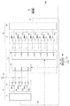
図1は、本発明の実施の形態に係るADコンバータ100の構成を示すブロック図である。
ADコンバータ100は、2ステップフラッシュ型のADコンバータであって、入力端子102に入力されるアナログ入力信号Vinを4ビットで量子化して、出力端子104からデジタル出力信号Voutを出力する。
(First embodiment)
FIG. 1 is a block diagram showing a configuration of an AD converter 100 according to an embodiment of the present invention.
The AD converter 100 is a two-step flash AD converter that quantizes the analog input signal Vin input to the
ADコンバータ100は、第1変換部10、第2変換部20、基準電圧回路30、合成回路40、監視部50を含む。2ステップフラッシュ型のADコンバータは、第1ステップとして、第1変換部10によって、複数の粗い基準電圧Vrcとアナログ入力信号Vinを比較し、上位2ビットを生成する。つぎに、第2ステップとして、第2変換部20によって複数の密な基準電圧Vrfとアナログ入力信号Vinを比較して下位2ビットを生成する。合成回路40は、上位2ビットと下位2ビットを合成してデジタル信号を出力する。粗い基準電圧Vrcおよび密な基準電圧Vrcは、基準電圧回路30によって生成される。
The AD converter 100 includes a
基準電圧回路30は、第1基準電圧生成部32、第2基準電圧生成部34を含む。第1基準電圧生成部32は、上位2ビットを生成する第1変換部10に対して、粗い基準電圧Vrc1〜Vrc3を出力する。第2基準電圧生成部34は、下位2ビットを生成する第2変換部20に対して、密な基準電圧Vrf1〜Vrf7を出力する。
The
図2は、第1基準電圧生成部32および第2基準電圧生成部34により生成される粗い基準電圧Vrcおよび密な基準電圧Vrfの初期値を示す図である。
FIG. 2 is a diagram illustrating initial values of the coarse reference voltage Vrc and the fine reference voltage Vrf generated by the first reference
第1基準電圧生成部32は、量子化値4、8、12に対応する粗い基準電圧Vrc1〜Vrc3を生成する。4ビットのA/Dコンバータにおいて、1LSBに相当する電圧ΔVrは、全入力電圧範囲Vfsrを用いて、ΔVr=Vfsr/24=Vfsr/16で与えられる。したがって、粗い基準電圧Vrc1〜Vrc3はそれぞれ、Vrc1=4×ΔVr、Vrc2=8×ΔVr、Vrc3=12×ΔVrとなる。粗い基準電圧Vrc1〜Vrc3は、第1変換部10へと出力される。
The first reference
本実施の形態では、全入力電圧範囲Vfsr=1.6Vとし、ΔVr=0.1Vの場合について説明する。このとき、第1基準電圧生成部32から生成される粗い基準電圧は、Vrc1=0.4V、Vrc2=0.8V、Vrc3=1.2Vとなる。
In the present embodiment, the case where the entire input voltage range Vfsr = 1.6 V and ΔVr = 0.1 V will be described. At this time, the rough reference voltages generated from the first reference
図1に戻る。第1変換部10は、第1比較部12および第1補正回路14を含む。
第1比較部12は3つのコンパレータCMPc1〜CMPc3を備え、それぞれには、第1基準電圧生成部32から出力される粗い基準電圧Vrc1〜Vrc3が入力されている。コンパレータCMPc1〜CMPc3はそれぞれ、アナログ入力信号Vinと粗い基準電圧Vrc1〜Vrc3を比較する。各コンパレータCMPc1〜CMPc3は、Vin>Vrcのときハイレベルを、Vin<Vrcのときローレベルを出力する。コンパレータCMPc1〜CMPc3による電圧比較の結果は、出力信号Sc1〜Sc3として出力される。
Returning to FIG. The
The
第1比較部12における電圧比較の結果、アナログ入力信号Vinが量子化値の0〜4、4〜8、8〜12、12〜16のいずれの範囲に含まれるのかが判定される。たとえば、量子化値0〜4の範囲に含まれる場合、Sc1〜Sc3はすべてローレベルとなる。量子化値4〜8の範囲に含まれる場合、出力信号Sc1はハイレベルとなり、出力信号Sc2、Sc3はローレベルとなる。第1比較部12は、コンパレータCMPc1〜CMPc3の出力信号Sc1〜Sc3を第1補正回路14に送出する。
As a result of the voltage comparison in the
第1補正回路14は、第1比較部12から出力される出力信号Sc1〜Sc3にもとづいて、ビット誤りなどを修正する。たとえば、第1比較部12から出力された出力信号Sc1〜Sc3をチェックし、出力信号Sc1、Sc3がローレベルであり、出力信号Sc2がハイレベルであった場合、出力信号Sc2をローレベルに設定し直すなどの処理を行う。第1補正回路14からは、補正後の出力信号Sc1’〜Sc3’が出力される。
このようにして生成された出力信号Sc1’〜Sc3’は、デジタル入力信号Vinを量子化したデジタルデータの上位2ビットを表している。
The
The output signals Sc1 ′ to Sc3 ′ thus generated represent the upper 2 bits of the digital data obtained by quantizing the digital input signal Vin.
第1補正回路14は、補正後の出力信号Sc1’〜Sc3’を合成回路40および第2基準電圧生成部34へ出力する。なお、図中、合成回路40および第2基準電圧生成部34へと出力される補正後の出力信号Sc’は、実際には3個の出力信号Sc1’〜Sc3’が簡略化して示されたものである。
The
第2変換部20は、第1変換部10による上位2ビットの生成後、下位2ビットを生成する変換部であって、第2比較部22および第2補正回路24を含む。
The
第1比較部12に用いられるコンパレータCMPc1〜CMPc3は、オフセットを有する場合があり、2つの入力電圧のいずれかが高い状態を平衡状態として動作することになる。
本明細書においてオフセット電圧Vofsの正負は、コンパレータの+側の入力端子に加算される電圧を正の向きにとるものとする。たとえば、コンパレータCMPc1にオフセット電圧Vofsが生じている場合、コンパレータは実質的に(Vin+Vofs)と基準電圧Vrc1を比較し、大小関係を判断する。
The comparators CMPc1 to CMPc3 used in the
In this specification, the positive / negative of the offset voltage Vofs means that the voltage added to the + side input terminal of the comparator is in the positive direction. For example, when the offset voltage Vofs is generated in the comparator CMPc1, the comparator substantially compares (Vin + Vofs) with the reference voltage Vrc1, and determines the magnitude relationship.
コンパレータCMPc1〜CMPc3の電圧比較においては、このオフセットによって、アナログ入力信号Vinと粗い基準電圧Vrc1〜Vrc3の比較結果に誤りが生ずることになる。たとえばアナログ入力信号Vin=0.35Vであるにもかかわらず、コンパレータCMPc1に1LSBに相当するΔVr=0.1Vのオフセット電圧Vofsが発生していた場合、本来量子化値0〜4の範囲に含まれると判定されるべきであるにもかかわらず、量子化値4〜8の範囲であると判定されることになる。 In the voltage comparison of the comparators CMPc1 to CMPc3, this offset causes an error in the comparison result between the analog input signal Vin and the rough reference voltages Vrc1 to Vrc3. For example, when the analog input signal Vin = 0.35V but the offset voltage Vofs of ΔVr = 0.1V corresponding to 1LSB is generated in the comparator CMPc1, it is originally included in the range of quantized values 0-4. In spite of the fact that it should be determined that the value is in the range of the quantized value 4-8.
第2比較部22は、下位2ビットを判定する際に、第1比較部12のコンパレータCMPc1〜CMPc3のオフセットによる誤差を低減するため、上位ビットの1LSB(下位ビットの4LSB)の範囲に加え、±2LSBのオーバーラップ範囲を加えた4+2+2=8LSBの範囲で電圧比較を行う。
すなわち、第1変換部10による上位2ビットの判定の結果、量子化値が4×nから4×n+4の間であると判定されたとすると、第2変換部20は、4×n−2から4×n+2の各量子化値について大小関係の判定を行う。
In order to reduce the error due to the offset of the comparators CMPc1 to CMPc3 of the
That is, if it is determined that the quantization value is between 4 × n and 4 × n + 4 as a result of the determination of the upper 2 bits by the
たとえば、第1変換部10の判定の結果、n=2であると判定された場合、量子化値は8〜12の間をとるはずであるが、本実施の形態に係るADコンバータ100では、第2変換部20において、量子化値6〜14の範囲について判定を行うこととなる。
For example, if it is determined that n = 2 as a result of the determination by the
±2LSBのオーバーラップ範囲を含む8LSBの範囲で電圧比較を行い下位ビットを判定するために、第2比較部22は、7個のコンパレータCMPf1〜CMPf7を含む。これらのコンパレータCMPfには、第2基準電圧生成部34により生成される密な基準電圧Vrf1〜Vrf7が入力されている。コンパレータCMPf1〜CMPf7はそれぞれ、密な基準電圧Vrf1〜Vrf7とアナログ入力信号Vinを比較し、Vin>Vrcのときハイレベルを、Vin<Vrcのときローレベルを出力する。コンパレータCMPf1〜CMPf7の出力をそれぞれ出力信号Sf1〜Sf7とする。
The
第2基準電圧生成部34は、第1補正回路14から出力される補正後の出力信号Sc’にもとづいて、1LSB(ΔVr=0.1V)刻みの密な基準電圧Vrf1〜Vrf7を生成する。
図2に示すように、第2基準電圧生成部34により生成される密な基準電圧Vrfの範囲は、上位2ビットに応じて変化する。図中nで示される数は、第1変換部10により生成された上位2ビットを10進数で表したものである。
たとえばn=0のとき、すなわち、アナログ入力信号Vinが、量子化値0〜4の範囲に含まれると判定されたとき、第2基準電圧生成部34は、オーバーラップ範囲を加えた量子化値0〜6に相当する密な基準電圧Vrfを生成する。n=1のとき、第2基準電圧生成部34は、量子化値3〜9に相当する密な基準電圧を生成する。n=2のときは、量子化値7〜13に相当する密な基準電圧を生成する。n=3のときは、量子化値11〜16に相当する密な基準電圧を生成する。
The second reference
As shown in FIG. 2, the range of the dense reference voltage Vrf generated by the second reference
For example, when n = 0, that is, when it is determined that the analog input signal Vin is included in the range of the quantization values 0 to 4, the second reference
具体的には、n=2のとき、第2基準電圧生成部34により生成される密な基準電圧の初期値は、Vrf1=3×ΔVr=0.3V、Vrf2=4×ΔVr=0.4V、Vrf3=5×ΔVr=0.5V、Vrf4=6×ΔVr=0.6V、Vrf5=7×ΔVr=0.7V、Vrf6=8×ΔVr=0.8V、Vrf7=9×ΔVr=0.9Vとなる。
このように第2基準電圧生成部34は上位2ビットに応じた密な基準電圧Vrf1〜Vrf7を生成し、第2変換部20へと出力する。
Specifically, when n = 2, the initial value of the dense reference voltage generated by the second reference
As described above, the second reference
第2比較部22から出力される下位2ビットに相当する出力信号Sf1〜Sf7は、第2補正回路24へと送出される。第2補正回路24は第1補正回路14と同様に、ビット誤りなどの訂正を行い、訂正後の出力信号Sf’を合成回路40に出力する。
Output signals Sf <b> 1 to Sf <b> 7 corresponding to the lower 2 bits output from the
合成回路40は、上位2ビットを表す出力信号Sc1’〜Sc3’と、下位2ビットを表す出力信号Sf1’〜Sf7’を合成してアナログ入力信号Vinをデジタル変換した4ビットのデジタル出力信号Voutを出力する。
The
つぎに、監視部50について説明する。
上述のように、第2変換部20の第2比較部22において、コンパレータCMPc1〜CMPc3にオフセットが生じた場合にも、正常なアナログデジタル変換が行えるように、±2LSBのオーバーラップ範囲を設けている。しかしながら、コンパレータのオフセットは、個体差、温度依存性、電源電圧変動、経時劣化などのさまざまな要因によって変動するため、必ずしも設計段階で設定したオーバーラップ範囲に入るとは限らない。さらに、理想的なADコンバータにおいて下位2ビットを判定するために必要なコンパレータは3つであるのに対し、オーバーラップ範囲を設けることによって、第2比較部22のコンパレータの数が7つに増えており、消費電流が増加してしまうという問題がある。
Next, the
As described above, in the
そこで、監視部50は、下位2ビットを表す第2補正回路24から出力される補正後の出力信号Sf’をモニタし、下位ビットのデータがオーバーラップ範囲に含まれているかどうかを判定する。監視部50により下位ビットをモニタすることにより、第1比較部12のコンパレータCMPc1〜CMPc3のオフセット電圧Vofsを予測することができる。
Therefore, the
第1変換部10による上位2ビットの判定の結果、量子化値8〜12の範囲(0.8V<Vin<1.2V)に含まれると判定されたにもかかわらず、第2比較部22における電圧比較の結果、量子化値7〜8の範囲(0.7V<Vin<0.8V)であると判定された場合には、第1比較部12のコンパレータCMPcにおいて、1LSBに相当するΔVr=0.1Vの正のオフセット電圧Vofsが生じていると予測される。
As a result of the determination of the upper 2 bits by the
逆に、第1変換部10による上位2ビットの判定の結果、量子化値4〜8の範囲(すなわち0.4V<Vin<0.8V)に含まれると判定されたとき、第2比較部22における電圧比較の結果、量子化値9〜10の範囲(0.9V<Vin<1.0V)であると判定された場合には、第1比較部12のコンパレータCMPcにおいて、−2LSBに相当する電圧Vofs=−2×ΔVr=−0.2Vの負のオフセットが生じていると予測される。
すなわち、下位ビットが、下側のオーバーラップ範囲に含まれた場合、オフセット電圧Vofsは正となり、上側のオーバーラップ範囲に含まれた場合オフセット電圧Vofsは負となることがわかる。
On the contrary, when it is determined that the
That is, it can be seen that when the lower bit is included in the lower overlap range, the offset voltage Vofs is positive, and when it is included in the upper overlap range, the offset voltage Vofs is negative.
監視部50は所定の学習期間の間、出力信号Sf’、すなわち下位2ビットをモニタし、第1変換部10により判定された範囲に含まれているか、あるいはオーバーラップ範囲に含まれているかの情報を蓄積し、第1比較部12のコンパレータCMPcのオフセット電圧Vofsを予測する。所定の学習期間は、たとえば、ADコンバータ100の起動後のアナログデジタル変換を行った回数により規定してもよいし、起動後の動作時間で規定してもよい。
The
監視部50は、学習期間に蓄積した第1比較部12のコンパレータCMPc1〜CMPc3のオフセット電圧Vofsの平均値を算出し、何LSBに相当するオフセット電圧を有するかをオフセット信号OFSとして第1基準電圧生成部32へ出力する。たとえば、オフセット電圧Vofs=0.1Vのとき、OFS=1となり、Vofs=−0.2Vのとき、OFS=−2となる。
The
第1基準電圧生成部32は、学習期間における監視の結果、コンパレータCMPc1〜CMPc3において平均値として1LSB=0.1Vのオフセット電圧Vofsが発生していると予測された場合には、粗い基準電圧Vrc1〜Vrc3を図2に示す初期値から1LSBに相当する電圧ΔVr=0.1Vだけ高電圧側へシフトして出力する。すなわち、第1基準電圧生成部32から出力される粗い基準電圧は、Vrc1=0.5V、Vrc2=0.9V、Vrc3=1.3Vとなる。
When it is predicted that the offset voltage Vofs of 1LSB = 0.1V is generated as an average value in the comparators CMPc1 to CMPc3 as a result of monitoring during the learning period, the first reference
逆に、学習期間におけるオフセット量のモニタの結果、コンパレータCMPc1〜CMPc3において平均値として−2LSBのオフセットが発生していると予測された場合には、粗い基準電圧Vrc1〜Vrc3を、図2に示す初期値から2LSBに相当する電圧2×ΔVr=0.2V分だけ低電圧側へとシフトして出力する。このとき、粗い基準電圧は、Vrc1=0.2V、Vrc2=0.6V、Vrc3=1.0Vとなる。
On the other hand, when it is predicted that an offset of −2 LSB is generated as an average value in the comparators CMPc1 to CMPc3 as a result of monitoring the offset amount during the learning period, rough reference voltages Vrc1 to Vrc3 are shown in FIG. A
第1比較部12のコンパレータCMPc1〜CMPc3は、コンパレータが有するオフセット分だけシフトした粗い基準電圧Vrc1〜Vrc3と、アナログ入力信号Vinを比較することになる。その結果、コンパレータCMPc1〜CMPc3のオフセットが見かけ上キャンセルされ、コンパレータCMPc1〜CMPc3による上位2ビットの判定の精度が向上し、ADコンバータ100のリニアリティを改善することができる。
The comparators CMPc1 to CMPc3 of the
このように、本実施の形態に係るADコンバータ100によれば、コンパレータCMPc1〜CMPc3のオフセットに応じて粗い基準電圧Vrc1〜Vrc3をシフトすることにより、上位2ビットの判定の精度が向上する。上位2ビットの判定に誤りがなければ、下位ビットの判定に際し、オーバーラップ範囲を狭めることが可能となる。 As described above, according to the AD converter 100 according to the present embodiment, the coarse reference voltages Vrc1 to Vrc3 are shifted according to the offsets of the comparators CMPc1 to CMPc3, thereby improving the accuracy of the determination of the upper 2 bits. If there is no error in the determination of the upper 2 bits, the overlap range can be narrowed when determining the lower bits.
さらに、本実施の形態に係るADコンバータ100は、学習期間においてオフセット量を決定し、粗い基準電圧Vrc1〜Vrc3をシフトした後、第2比較部22のコンパレータCMPf1〜CMPf7のうち、オーバーラップ範囲に設けられたコンパレータCMPf1、CMPf7をオフする。すなわちオーバーラップ範囲は±1LSBに狭められる。
コンパレータCMPcのオフセットが安定している場合には、さらに、コンパレータCMPf2、CMPf6をオフし、オーバーラップ範囲を0LSBとしてもよい。
Further, the AD converter 100 according to the present embodiment determines the offset amount in the learning period, shifts the rough reference voltages Vrc1 to Vrc3, and then enters the overlap range of the comparators CMPf1 to CMPf7 of the
When the offset of the comparator CMPc is stable, the comparators CMPf2 and CMPf6 may be turned off and the overlap range may be set to 0LSB.
このように本実施の形態に係るADコンバータ100によれば、学習期間の終了後、オーバーラップ範囲に設けられたコンパレータCMPcをオフすることにより、消費電流を低減することができる。 As described above, according to the AD converter 100 according to the present embodiment, the current consumption can be reduced by turning off the comparator CMPc provided in the overlap range after the end of the learning period.
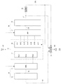
(第2の実施形態)
図3は、第2の実施形態に係るADコンバータ200の構成を示すブロック図である。図3において、図1と同一の構成要素には同一の符号を付し、適宜重複した説明を省略するものとする。
本実施の形態に係るADコンバータ200は、監視部50による下位ビットを表す出力信号Sc’のモニタしてコンパレータCMPc1〜CMPc3のオフセット電圧Vofsを予測し、第2基準電圧生成部34により生成される密な基準電圧Vrfをシフトする。
(Second Embodiment)
FIG. 3 is a block diagram illustrating a configuration of the
The
第1比較部12のコンパレータCMPc1〜CMPc3は、必ずしも同一のオフセットを有するとは限らず、異なったオフセット量を有する場合がある。たとえば、コンパレータCMPc1のみがVofs1=+ΔVr=0.1Vのオフセットを有し、コンパレータCMPc2およびCMPc3はオフセットをもたない場合も考えられる。
そのため、監視部50は、第2補正回路24から出力される補正後の出力信号Sf’をモニタし、第1比較部12のコンパレータCMPc1〜CMPc3ごとのそれぞれのオフセット電圧Vofs1〜Vofs3を予測する。
The comparators CMPc1 to CMPc3 of the
Therefore, the
監視部50は、学習期間におけるモニタの結果、コンパレータCMPc1〜CMPc3がそれぞれ有するオフセット電圧Vofs1〜Vofs3を予測し、何LSBに相当する電圧がオフセットしているかをオフセット信号OFS1〜OFS3として第2基準電圧生成部34に出力する。たとえば、コンパレータCMPc2に0.1Vのオフセットが生じていると予測された場合、OFS2=1を出力する。
The
第2基準電圧生成部34は、学習期間の終了後、監視部50により予測されたオフセット電圧Vofs1〜Vofs3を表すオフセット信号OFS1〜OFS3にもとづいて、密な基準電圧Vrf1〜Vrf7をシフトする。
たとえば、n=0のときの密な基準電圧Vrfについては、コンパレータCMPc1のオフセット電圧Vofs1にもとづいてシフトさせる。たとえば、オフセット電圧Vofs1=+0.1Vのとき、図2に示す密な基準電圧Vrfの初期値から0.1Vだけ低電圧側にシフトする。
After the end of the learning period, the second reference
For example, the dense reference voltage Vrf when n = 0 is shifted based on the offset voltage Vofs1 of the comparator CMPc1. For example, when the offset voltage Vofs1 = + 0.1V, the initial value of the dense reference voltage Vrf shown in FIG. 2 is shifted to the low voltage side by 0.1V.
n=1のときには、コンパレータCMPc1、CMPc2のオフセット電圧Vofs1、Vofs2にもとづいて密な基準電圧Vrfをシフトさせる。n=2のときには、コンパレータCMPc2、CMPc3のオフセット電圧Vofs2、Vofs3にもとづいて密な基準電圧Vrfをシフトさせる。n=3のときには、コンパレータCMPc3のオフセット電圧Vofs3にもとづいて密な基準電圧Vrfをシフトさせる。 When n = 1, the dense reference voltage Vrf is shifted based on the offset voltages Vofs1, Vofs2 of the comparators CMPc1, CMPc2. When n = 2, the dense reference voltage Vrf is shifted based on the offset voltages Vofs2 and Vofs3 of the comparators CMPc2 and CMPc3. When n = 3, the fine reference voltage Vrf is shifted based on the offset voltage Vofs3 of the comparator CMPc3.
たとえば、監視部50によるモニタの結果、コンパレータCMPc1にのみ1LSBに相当するオフセット電圧Vofs1=0.1Vが生じていることが予測された場合、第2基準電圧生成部34は、n=0のときの密な基準電圧Vrfを、図2に示す初期状態から1LSBに相当する電圧ΔVr分だけ低電圧側へとシフトして出力する。またn=1のときの密な基準電圧Vrfについても、図2に示す初期状態から電圧ΔVr分だけシフトして出力する。n=2、n=3のときの基準電圧Vrfについては、図2に示す初期値の値をそのまま出力する。
For example, when it is predicted that the offset voltage Vofs1 = 0.1 V corresponding to 1LSB is generated only in the comparator CMPc1 as a result of monitoring by the
密な基準電圧Vrfがシフトされる結果、コンパレータCMPf1〜CMPf7から出力される出力信号Sf1〜Sf7に対応するビットが基準電圧のシフト前と比べて変化することになる。出力信号Sf1〜Sf7を正確な下位ビットに変換するため、監視部50により予測されたオフセット電圧Vofs1〜Vofs3を表すオフセット信号OFS1〜OFS3は、合成回路40にも出力される。合成回路40は、オフセット信号OFS1〜OFS3にもとづいて、出力信号Sf’を適切に下位2ビットに変換して上位2ビットを表す出力信号Sc’と合成する。
As a result of the dense reference voltage Vrf being shifted, the bits corresponding to the output signals Sf1 to Sf7 output from the comparators CMPf1 to CMPf7 change compared to before the reference voltage is shifted. In order to convert the output signals Sf1 to Sf7 into accurate lower bits, the offset signals OFS1 to OFS3 representing the offset voltages Vofs1 to Vofs3 predicted by the
このように、本実施の形態に係るADコンバータ200によれば、第2基準電圧生成部34により生成される密な基準電圧Vrfを、第1比較部12のコンパレータCMPcのオフセットに応じてシフトさせることにより、コンパレータCMPc1〜CMPc3それぞれのオフセット電圧Vofsを個別に補正することができる。
As described above, according to the
本実施の形態に係るADコンバータ200によれば、第2変換部20における下位ビットの生成時に、第1変換部10により生成された上位ビットの範囲で電圧比較を行うことになるため、リニアリティを改善することができる。
According to the
第2の実施の形態に係るADコンバータ200においても、学習期間の完了後、第2比較部22のコンパレータCMPfのうち、オーバーラップ範囲に設けられたCMPf1、CMPf7、さらにCMPf2、CMPf6をオフしてもよい。コンパレータをオフすることにより消費電流を低減することができる。
Also in the
第2の実施形態のようにコンパレータCMPcのオフセットの予測結果を第2基準電圧生成部34に出力する場合においても、第1の実施形態と同様に、密な基準電圧Vrfを一様にシフトしてもよい。
Even when the prediction result of the offset of the comparator CMPc is output to the second
最後に、第1、第2の実施形態において、第1基準電圧生成部32または第2基準電圧生成部34において基準電圧Vrc、Vrfをシフトする方法について説明する。
Finally, in the first and second embodiments, a method of shifting the reference voltages Vrc and Vrf in the first reference
ADコンバータの基準電圧回路は、抵抗値の等しく設定された複数の抵抗を直列に接続し、その両端に最大電圧Vref1および最小電圧Vref2を印加する。基準電圧回路は、各抵抗の接続ノードに現れる抵抗分圧され電位差が等しい複数の電圧を基準電圧として第1比較部12、第2比較部22へと出力する。
したがって、監視部50により予測されたオフセットにもとづいて、最大電圧Vref1および最小電圧Vref2をシフトさせることにより、第1基準電圧生成部32あるいは第2基準電圧生成部34に出力する基準電圧をシフトすることができる。
The reference voltage circuit of the AD converter connects a plurality of resistors having equal resistance values in series, and applies a maximum voltage Vref1 and a minimum voltage Vref2 to both ends thereof. The reference voltage circuit outputs, to the
Accordingly, the reference voltage output to the first reference
また、最大電圧Vref1および最小電圧Vref2を固定しておき、粗い基準電圧Vrcまたは密な基準電圧Vrfを出力する電圧出力端子と複数の抵抗の接続ノード間にスイッチを設け、スイッチの接続状態を切り替えることによっても、オフセットに応じて基準電圧Vrc、Vrfをシフトさせることができる。 Further, the maximum voltage Vref1 and the minimum voltage Vref2 are fixed, a switch is provided between a voltage output terminal that outputs the rough reference voltage Vrc or the fine reference voltage Vrf and a connection node of a plurality of resistors, and the connection state of the switches is switched. Also, the reference voltages Vrc and Vrf can be shifted according to the offset.
上記実施の形態は例示であり、それらの各構成要素や各処理プロセスの組合せにいろいろな変形例が可能なこと、またそうした変形例も本発明の範囲にあることは当業者に理解されるところである。 Those skilled in the art will understand that the above-described embodiment is an exemplification, and that various modifications can be made to combinations of the respective constituent elements and processing processes, and such modifications are also within the scope of the present invention. is there.
実施の形態の形態においては、監視部50は、所定の学習期間の間、出力信号Sf’をモニタする場合について説明したがこれには限定されない。たとえば、監視部50により、ADコンバータ100、200の動作中、継続して出力信号Sf’をモニタしておくことにより、温度変動などによってコンパレータCMPcのオフセットが変化した場合にも、変動後のオフセット量に応じて基準電圧Vrc、Vrfを生成することができる。
In the embodiment, the case where the
第1の実施形態においては、第1基準電圧生成部32により生成される粗い基準電圧Vrcをシフトし、第2の実施形態においては第2基準電圧生成部34により生成される密な基準電圧Vrfをシフトする場合について説明したが、粗い基準電圧Vrcおよび密な基準電圧Vrfを、コンパレータCMPcのオフセットに応じて同時にシフトさせてもよい。この場合、第1基準電圧生成部32または第2基準電圧生成部34のいずれかにより補正を行う場合に比べて、より自由度の高い補正を行うことができる。
In the first embodiment, the coarse reference voltage Vrc generated by the first
第1の実施形態において第1基準電圧生成部32は、コンパレータCMPc1〜CMPc3のオフセットの平均値にもとづいて、粗い基準電圧Vrc1〜Vrc3を一様にシフトさせる場合について説明したがこれには限定されず、第2の実施形態のように、各コンパレータCMPc1〜CMPc3それぞれのオフセットにもとづいて粗い基準電圧Vrc1〜Vrc3を個別にシフトしてもよい。
In the first embodiment, the first reference
第1、第2の実施の形態においては、説明を簡略化するために、4ビットのADコンバータについて説明したがこれには限定されない。8ビット、あるいはより大きなビット数を有するADコンバータにおいては、コンパレータCMPcのオフセットが、リニアリティなどに大きく影響するため、4ビットの場合よりもさらに本発明の効果を得ることができる。 In the first and second embodiments, the 4-bit AD converter has been described in order to simplify the description, but the present invention is not limited to this. In an AD converter having 8 bits or a larger number of bits, the offset of the comparator CMPc greatly affects the linearity and the like, so that the effect of the present invention can be obtained more than in the case of 4 bits.
100 ADコンバータ、 200 ADコンバータ、 10 第1変換部、 12 第1比較部、 14 第1補正回路、 20 第2変換部、 22 第2比較部、 24 第2補正回路、 CMPc コンパレータ、 CMPf コンパレータ、 30 基準電圧回路、 32 第1基準電圧生成部、 34 第2基準電圧生成部、 40 合成回路、 50 監視部。 100 AD converter, 200 AD converter, 10 first conversion unit, 12 first comparison unit, 14 first correction circuit, 20 second conversion unit, 22 second comparison unit, 24 second correction circuit, CMPc comparator, CMPf comparator, 30 reference voltage circuit, 32 first reference voltage generation unit, 34 second reference voltage generation unit, 40 synthesis circuit, 50 monitoring unit.
Claims (8)
複数の粗い基準電圧を生成する第1基準電圧生成部と、
前記複数の粗い基準電圧と前記アナログ入力信号を比較し、上位ビットのデータを生成する第1変換部と、
前記第1変換部により生成された上位ビットのデータ範囲にオーバーラップ範囲を加えた範囲全体に渡って、複数の密な基準電圧を生成する第2基準電圧生成部と、
前記複数の密な基準電圧と前記アナログ入力信号を比較し、下位ビットのデータを生成する第2変換部と、
前記第2変換部により生成された下位ビットのデータを監視する監視部と、を備え、
前記第1基準電圧生成部は、前記監視部による監視の結果、前記下位ビットのデータが上側のオーバーラップ範囲に含まれた場合には、前記複数の粗い基準電圧を低電圧側にシフトし、下側のオーバーラップ範囲に含まれた場合には、前記複数の粗い基準電圧を高電圧側にシフトすることを特徴とするアナログデジタル変換器。 A two-step flash type analog-digital converter that converts an analog input signal into two stages of an upper bit and a lower bit for digital conversion,
A first reference voltage generator that generates a plurality of coarse reference voltages;
A first converter that compares the plurality of coarse reference voltages with the analog input signal and generates high-order bit data;
A second reference voltage generation unit for generating a plurality of dense reference voltages over the entire range obtained by adding an overlap range to the data range of the upper bits generated by the first conversion unit;
A second converter for comparing the plurality of dense reference voltages with the analog input signal and generating lower-bit data;
A monitoring unit that monitors lower bit data generated by the second conversion unit,
The first reference voltage generation unit shifts the plurality of coarse reference voltages to a low voltage side when the lower bit data is included in the upper overlap range as a result of monitoring by the monitoring unit, An analog-to-digital converter characterized by shifting the plurality of rough reference voltages to a high voltage side when included in a lower overlap range.
前記第1基準電圧生成部は、前記監視部の監視結果にもとづき、適応的に前記複数の粗い基準電圧をシフトすることを特徴とする請求項1に記載のアナログデジタル変換器。 The monitoring unit continuously monitors the data of the lower bits during the operation of the circuit;
The analog-to-digital converter according to claim 1, wherein the first reference voltage generation unit adaptively shifts the plurality of coarse reference voltages based on a monitoring result of the monitoring unit.
前記第1基準電圧生成部は、前記学習期間中の監視結果にもとづいて、前記複数の粗い基準電圧のシフト量を決定することを特徴とする請求項1に記載のアナログデジタル変換器。 The monitoring unit monitors the data of the lower bits during a predetermined learning period;
2. The analog-digital converter according to claim 1, wherein the first reference voltage generation unit determines shift amounts of the plurality of coarse reference voltages based on a monitoring result during the learning period.
複数の粗い基準電圧を生成する第1基準電圧生成部と、
前記複数の粗い基準電圧と前記アナログ入力信号を比較し、上位ビットのデータを生成する第1変換部と、
前記第1変換部により生成された上位ビットのデータ範囲にオーバーラップ範囲を加えた範囲全体に渡って、複数の密な基準電圧を生成する第2基準電圧生成部と、
前記複数の密な基準電圧と前記アナログ入力信号を比較し、下位ビットのデータを生成する第2変換部と、
前記第2変換部により生成された下位ビットのデータを監視する監視部と、を備え、
前記第2基準電圧生成部は、前記監視部による監視の結果、前記下位ビットのデータが上側のオーバーラップ範囲に含まれた場合には、前記複数の密な基準電圧を高電圧側にシフトし、下側のオーバーラップ範囲に含まれた場合には、前記複数の密な基準電圧を低電圧側にシフトすることを特徴とするアナログデジタル変換器。 A two-step flash type analog-digital converter that converts an analog input signal into two stages of an upper bit and a lower bit for digital conversion,
A first reference voltage generator that generates a plurality of coarse reference voltages;
A first converter that compares the plurality of coarse reference voltages with the analog input signal and generates high-order bit data;
A second reference voltage generation unit for generating a plurality of dense reference voltages over the entire range obtained by adding an overlap range to the data range of the upper bits generated by the first conversion unit;
A second converter for comparing the plurality of dense reference voltages with the analog input signal and generating lower-bit data;
A monitoring unit that monitors lower bit data generated by the second conversion unit,
The second reference voltage generator shifts the plurality of dense reference voltages to the high voltage side when the lower bit data is included in the upper overlap range as a result of monitoring by the monitoring unit. The analog-digital converter characterized by shifting the plurality of dense reference voltages to the low voltage side when included in the lower overlap range.
前記第2基準電圧生成部は、前記監視部の監視結果にもとづき、適応的に前記複数の密な基準電圧をシフトすることを特徴とする請求項4に記載のアナログデジタル変換器。 The monitoring unit continuously monitors the data of the lower bits during the operation of the circuit;
The analog-to-digital converter according to claim 4, wherein the second reference voltage generation unit adaptively shifts the plurality of dense reference voltages based on a monitoring result of the monitoring unit.
前記第2基準電圧生成部は、前記学習期間中の監視結果にもとづいて、前記複数の密な基準電圧のシフト量を決定することを特徴とする請求項4に記載のアナログデジタル変換器。 The monitoring unit monitors the data of the lower bits during a predetermined learning period;
5. The analog-to-digital converter according to claim 4, wherein the second reference voltage generation unit determines shift amounts of the plurality of dense reference voltages based on a monitoring result during the learning period.
Priority Applications (1)
| Application Number | Priority Date | Filing Date | Title |
|---|---|---|---|
| JP2004351249A JP4536498B2 (en) | 2004-12-03 | 2004-12-03 | Analog to digital converter |
Applications Claiming Priority (1)
| Application Number | Priority Date | Filing Date | Title |
|---|---|---|---|
| JP2004351249A JP4536498B2 (en) | 2004-12-03 | 2004-12-03 | Analog to digital converter |
Publications (2)
| Publication Number | Publication Date |
|---|---|
| JP2006165765A JP2006165765A (en) | 2006-06-22 |
| JP4536498B2 true JP4536498B2 (en) | 2010-09-01 |
Family
ID=36667311
Family Applications (1)
| Application Number | Title | Priority Date | Filing Date |
|---|---|---|---|
| JP2004351249A Expired - Fee Related JP4536498B2 (en) | 2004-12-03 | 2004-12-03 | Analog to digital converter |
Country Status (1)
| Country | Link |
|---|---|
| JP (1) | JP4536498B2 (en) |
Families Citing this family (3)
| Publication number | Priority date | Publication date | Assignee | Title |
|---|---|---|---|---|
| JP2009200931A (en) * | 2008-02-22 | 2009-09-03 | Panasonic Corp | Solid-state imaging apparatus, semiconductor integrated circuit device, and signal processing method |
| JP2011114785A (en) * | 2009-11-30 | 2011-06-09 | Renesas Electronics Corp | Solid-state imaging device |
| US11355184B2 (en) * | 2020-03-05 | 2022-06-07 | Silicon Storage Technology, Inc. | Analog neural memory array in artificial neural network with substantially constant array source impedance with adaptive weight mapping and distributed power |
Family Cites Families (2)
| Publication number | Priority date | Publication date | Assignee | Title |
|---|---|---|---|---|
| JPS5912618A (en) * | 1982-07-13 | 1984-01-23 | Nippon Telegr & Teleph Corp <Ntt> | Analog-digital converter |
| JPH09162738A (en) * | 1995-12-04 | 1997-06-20 | Matsushita Electric Ind Co Ltd | Series-parallel A / D converter |
-
2004
- 2004-12-03 JP JP2004351249A patent/JP4536498B2/en not_active Expired - Fee Related
Also Published As
| Publication number | Publication date |
|---|---|
| JP2006165765A (en) | 2006-06-22 |
Similar Documents
| Publication | Publication Date | Title |
|---|---|---|
| US8164504B2 (en) | Successive approximation register analog-digital converter and method for operating the same | |
| US8482446B2 (en) | A/D converter circuit, electronic apparatus and A/D conversion method | |
| US8319675B2 (en) | Analog-to-digital converter | |
| US8199041B2 (en) | Analog-to-digital converter | |
| US7576677B2 (en) | Pipeline A/D converter converting analog signal to digital signal | |
| US20050001747A1 (en) | All-analog calibration of string-DAC linearity: application to high voltage processes | |
| US8570206B1 (en) | Multi-bit per cycle successive approximation register ADC | |
| JP2018050282A (en) | Successive approximation resister ad converter | |
| US8542144B2 (en) | Analog to digital converter | |
| JP2013150117A (en) | Analog-digital converter and receiver | |
| US7579973B2 (en) | Analog-to-digital converter | |
| US7187317B2 (en) | A/D conversion apparatus | |
| CN101179273B (en) | Analog-to-Digital Converter | |
| KR20150107569A (en) | Ad conversion circuit | |
| JP4536498B2 (en) | Analog to digital converter | |
| JP4613929B2 (en) | A / D conversion circuit | |
| JP7499742B2 (en) | Power supply circuit and voltage detection circuit | |
| US6836237B2 (en) | Analog-to-digital converter | |
| JP2007266951A (en) | Analog to digital converter | |
| JP4551194B2 (en) | Analog to digital converter | |
| JP4519475B2 (en) | A / D converter | |
| Watabe et al. | Preliminary experiment for precise and dynamic digital calibration for two-stage cyclic ADC suitable for 33-Mpixel 120-fps 8K Super Hi-Vision CMOS image sensor | |
| JP2006148574A (en) | Analog/digital converter | |
| JP2017191964A (en) | AD converter circuit | |
| JP2007208423A (en) | Analog to digital converter |
Legal Events
| Date | Code | Title | Description |
|---|---|---|---|
| A621 | Written request for application examination |
Free format text: JAPANESE INTERMEDIATE CODE: A621 Effective date: 20071126 |
|
| A977 | Report on retrieval |
Free format text: JAPANESE INTERMEDIATE CODE: A971007 Effective date: 20100610 |
|
| TRDD | Decision of grant or rejection written | ||
| A01 | Written decision to grant a patent or to grant a registration (utility model) |
Free format text: JAPANESE INTERMEDIATE CODE: A01 Effective date: 20100615 |
|
| A01 | Written decision to grant a patent or to grant a registration (utility model) |
Free format text: JAPANESE INTERMEDIATE CODE: A01 |
|
| A61 | First payment of annual fees (during grant procedure) |
Free format text: JAPANESE INTERMEDIATE CODE: A61 Effective date: 20100616 |
|
| FPAY | Renewal fee payment (event date is renewal date of database) |
Free format text: PAYMENT UNTIL: 20130625 Year of fee payment: 3 |
|
| R150 | Certificate of patent or registration of utility model |
Free format text: JAPANESE INTERMEDIATE CODE: R150 |
|
| LAPS | Cancellation because of no payment of annual fees |