JP4535429B2 - Manufacturing method of semiconductor device - Google Patents
Manufacturing method of semiconductor device Download PDFInfo
- Publication number
- JP4535429B2 JP4535429B2 JP2004158626A JP2004158626A JP4535429B2 JP 4535429 B2 JP4535429 B2 JP 4535429B2 JP 2004158626 A JP2004158626 A JP 2004158626A JP 2004158626 A JP2004158626 A JP 2004158626A JP 4535429 B2 JP4535429 B2 JP 4535429B2
- Authority
- JP
- Japan
- Prior art keywords
- electrode
- layer
- solder
- semiconductor device
- manufacturing
- Prior art date
- Legal status (The legal status is an assumption and is not a legal conclusion. Google has not performed a legal analysis and makes no representation as to the accuracy of the status listed.)
- Expired - Lifetime
Links
Images


Landscapes
- Electric Connection Of Electric Components To Printed Circuits (AREA)
- Lead Frames For Integrated Circuits (AREA)
Description
本発明は、リードフレーム等の電極に対して毒性の少ないPbフリーはんだ合金を用いて適するように接続するPbフリーはんだ接続構造体およびこれを用いた電子機器に関するものである。 The present invention relates to a Pb-free solder connection structure that is suitably connected to an electrode such as a lead frame using a Pb-free solder alloy having low toxicity, and an electronic device using the same.
従来、有機基板等の回路基板にLSI等の電子部品を接続して電子回路基板を製造するには、Sn−Pb共晶はんだ、及びこのSn−Pb共晶はんだ近傍で、融点も類似なSn−Pbはんだ、或いは、これらに少量のBiやAgを添加したはんだ合金が用いられている。これらのはんだには、Pbが約40重量%含まれている。いずれのこれらのはんだ合金も、融点はほぼ183℃であり、220〜240℃でのはんだ付けが可能である。 Conventionally, in order to manufacture an electronic circuit board by connecting an electronic component such as an LSI to a circuit board such as an organic substrate, Sn—Pb eutectic solder and Sn having a similar melting point in the vicinity of the Sn—Pb eutectic solder are used. -Pb solder or a solder alloy obtained by adding a small amount of Bi or Ag to these is used. These solders contain about 40% by weight of Pb. Any of these solder alloys has a melting point of approximately 183 ° C. and can be soldered at 220 to 240 ° C.
また、はんだ付けされるQFP(Quad Flat Package)−LSI等の電子部品の電極は、Fe−Ni系合金である42アロイ表面に90重量%Sn−10重量%Pb(以下Sn−10Pbと略す)層をめっき等で施した電極が一般的に用いられている。これは、はんだぬれ性が良好であり、且つ保存性が良く、ウィスカーの発生の問題がないためである。 Further, electrodes of electronic parts such as QFP (Quad Flat Package) -LSI to be soldered are 90 wt% Sn-10 wt% Pb (hereinafter abbreviated as Sn-10 Pb) on a 42 alloy surface which is an Fe—Ni alloy. An electrode having a layer formed by plating or the like is generally used. This is because solder wettability is good, storage is good, and there is no problem of whisker generation.
しかし、上記のSn−Pb系はんだ中に含まれているPbは人体に有毒な重金属であり、Pbを含む製品を廃棄することによる地球環境の汚染、生物への悪影響が問題となっている。この電気製品による地球環境の汚染は、野ざらしに放置されたPbを含む電気製品から、雨等によってPbが溶出することによって起こる。Pbの溶出は、最近の酸性雨によって加速される傾向にある。従って、環境汚染を低減するためには、大量に使用されている上記のSn−Pb共晶系はんだの代替としてPbを含まない低毒性のPbフリーはんだ材料、及び部品電極上で使用されているSn−10Pb層の代替材料としてPbを含まない部品電極構造が必要である。Pbフリーはんだ材料としては低毒性、材料供給性、コスト、ぬれ性、機械的性質、接続信頼性等と観点からSn−Ag−Bi系はんだが有力候補となっている。また、はんだ付けにおいては、通常、220〜240℃付近に加熱し、部品、基板の電極とはんだとの間に化合物を生成させることによって、接続を行っている。従って、形成される界面は、はんだ材料と部品側の電極材料の組み合わせによって異なるため、安定な接続界面を得るためには、そのはんだに適する電極材料が必要である。 However, Pb contained in the above Sn—Pb solder is a heavy metal that is toxic to the human body, and pollution of the global environment and adverse effects on living organisms due to the disposal of the product containing Pb are problematic. The pollution of the global environment by this electric product is caused by the elution of Pb by rain or the like from the electric product containing Pb left unattended. Pb elution tends to be accelerated by recent acid rain. Therefore, in order to reduce environmental pollution, Pb-free low-toxic Pb-free solder materials and component electrodes are used as an alternative to the Sn-Pb eutectic solders used in large quantities. A component electrode structure not containing Pb is required as an alternative material for the Sn-10Pb layer. As a Pb-free solder material, Sn—Ag—Bi solder is a promising candidate from the viewpoints of low toxicity, material supply, cost, wettability, mechanical properties, connection reliability, and the like. In soldering, the connection is usually made by heating to around 220 to 240 ° C. and generating a compound between the component, the electrode of the substrate and the solder. Therefore, since the formed interface differs depending on the combination of the solder material and the electrode material on the component side, an electrode material suitable for the solder is necessary to obtain a stable connection interface.
本発明の目的は、リードフレーム等の電極に対して毒性の少ないSn−Ag−Bi系のPbフリーはんだ合金を用いて十分な接続強度を有し、且つ安定な接続界面が得られるようにしたPbフリーはんだ接続構造体を提供することにある。 また、本発明の他の目的は、毒性の少ないSn−Ag−Bi系のPbフリーはんだ合金を用いて、電子部品、基板間の熱膨張係数の差、はんだ付け後の割基板作業、或いはプロービングテスト時の基板の反り、ハンドリング等によってはんだ接続部に発生する応力に耐え得る十分な接続強度を有し、且つ経時的にも安定な界面を得ることができるようにした電子機器を提供することにある。 An object of the present invention is to use Sn-Ag-Bi-based Pb-free solder alloy that is less toxic to an electrode such as a lead frame, so that a sufficient connection strength and a stable connection interface can be obtained. The object is to provide a Pb-free solder connection structure. Another object of the present invention is to use Sn-Ag-Bi-based Pb-free solder alloy with low toxicity, difference in thermal expansion coefficient between electronic components, substrates, split substrate work after soldering, or probing To provide an electronic device having a sufficient connection strength that can withstand stress generated in a solder connection portion due to warping of a substrate during testing, handling, etc., and being able to obtain a stable interface over time. It is in.
また、本発明の他の目的は、毒性の少ないSn−Ag−Bi系のPbフリーはんだ合金を用いて、十分なぬれ性を確保して十分な接続強度を有し、また耐ウィスカー性等も確保できるようにしたPbフリーはんだ接続構造体および電子機器を提供することにある。 Another object of the present invention is to use Sn-Ag-Bi-based Pb-free solder alloy with low toxicity, to ensure sufficient wettability and to have sufficient connection strength, whisker resistance, etc. An object is to provide a Pb-free solder connection structure and an electronic device that can be secured.
上記目的を達成するために、本発明は、Sn−Ag−Bi系のPbフリーはんだをSn−Bi系層を介して電極に接続したことを特徴とするPbフリーはんだ接続構造体である。 In order to achieve the above object, the present invention provides a Pb-free solder connection structure in which Sn-Ag-Bi-based Pb-free solder is connected to an electrode through an Sn-Bi-based layer.
また、本発明は、前記Pbフリーはんだ接続構造体におけるSn−Bi系層中のBi量は、1〜20重量%であることを特徴とする。 In the present invention, the amount of Bi in the Sn-Bi-based layer in the Pb-free solder connection structure is 1 to 20% by weight.
また、本発明は、前記Pbフリーはんだ接続構造体において、前記Sn−Bi系層と前記電極との間にCu層を有することを特徴とする。 In the Pb-free solder connection structure according to the present invention, a Cu layer is provided between the Sn—Bi-based layer and the electrode.
また、本発明は、前記Pbフリーはんだ接続構造体において、前記電極がCu材で形成されていることを特徴とする。 In the Pb-free solder connection structure, the present invention is characterized in that the electrode is formed of a Cu material.
また、本発明は、前記Pbフリーはんだ接続構造体における電極は、Fe−Ni系合金またはCu系のリードであることを特徴とする。 Further, the invention is characterized in that the electrode in the Pb-free solder connection structure is an Fe—Ni alloy or a Cu lead.
また、本発明は、前記Pbフリーはんだ接続構造体におけるSn−Ag−Bi系のPbフリーはんだは、Snを主成分として、Biが5〜25重量%、Agが1.5〜3重量%、Cuが0〜1重量%を含有することを特徴とする。 In the present invention, the Sn-Ag-Bi-based Pb-free solder in the Pb-free solder connection structure has Sn as a main component, Bi is 5 to 25% by weight, Ag is 1.5 to 3% by weight, Cu contains 0 to 1% by weight.
また、本発明は、電子部品に形成された第1の電極と、回路基板に形成された第2の電極とを電気的に接続する電子機器であって、前記第1の電極にSn−Bi系層を施し、該Sn−Bi系層を施した第1の電極と前記第2の電極とをSn−Ag−Bi系のPbフリーはんだで接続したことを特徴とする電子機器である。 According to another aspect of the present invention, there is provided an electronic apparatus that electrically connects a first electrode formed on an electronic component and a second electrode formed on a circuit board, the Sn-Bi being connected to the first electrode. The electronic device is characterized in that a system layer is applied, and the first electrode provided with the Sn-Bi system layer and the second electrode are connected with Sn-Ag-Bi system Pb-free solder.
また、本発明は、前記電子機器におけるSn−Bi系層中のBi量は、1〜20重量%であることを特徴とする。 The present invention is characterized in that the amount of Bi in the Sn-Bi-based layer in the electronic device is 1 to 20% by weight.
また、本発明は、前記電子機器において、前記Sn−Bi系層と第1の電極との間にCu層を有することを特徴とする。 In the electronic device, a Cu layer may be provided between the Sn—Bi-based layer and the first electrode.
また、本発明は、前記電子機器において、前記Sn−Bi系層の第1の電極側がCu材であることを特徴とする。 In the electronic device, the first electrode side of the Sn—Bi-based layer is a Cu material.
また、本発明は、前記電子機器における第1の電極は、Fe−Ni系合金またはCu系のリードであることを特徴とする。 According to the present invention, the first electrode in the electronic device is an Fe—Ni alloy or a Cu lead.
また、本発明は、前記電子機器におけるSn−Ag−Bi系のPbフリーはんだは、Snを主成分として、Biが5〜25重量%、Agが1.5〜3重量%、Cuが0〜1重量%を含有することを特徴とする。 In the present invention, the Sn-Ag-Bi-based Pb-free solder in the electronic device has Sn as a main component, Bi is 5 to 25% by weight, Ag is 1.5 to 3% by weight, and Cu is 0 to 0%. It contains 1% by weight.
また、本発明は、電極に接続されるPbフリーはんだとして、Snを主成分として、Biが5〜25重量%、Agが1.5〜3重量%、Cuが0〜1重量%を含有するSn−Ag−Bi系であることを特徴とするPbフリーはんだ接続構造体である。 Moreover, this invention contains Sn as a main component, Bi is 5 to 25 weight%, Ag is 1.5 to 3 weight%, Cu is 0 to 1 weight% as Pb free solder connected to an electrode. A Pb-free solder connection structure characterized by being based on Sn-Ag-Bi.
以上説明したように、前記構成によれば、リードフレーム等の電極に対して毒性の少ないSn−Ag−Bi系のPbフリーはんだ合金を用いて十分な接続強度を有し、且つ安定な接続界面を得ることができる。 As described above, according to the above configuration, a stable connection interface having a sufficient connection strength using a Sn-Ag-Bi based Pb-free solder alloy that is less toxic to an electrode such as a lead frame. Can be obtained.
また、前記構成によれば、毒性の少ないSn−Ag−Bi系のPbフリーはんだ合金を用いて、電子部品、基板間の熱膨張係数の差、はんだ付け後の割基板作業、或いはプロービングテスト時の基板の反り、ハンドリング等によってはんだ接続部に発生する応力に耐え得る十分な接続強度を有し、且つ経時的にも安定な界面を得ることができる。 In addition, according to the above configuration, when using a Sn-Ag-Bi-based Pb-free solder alloy with low toxicity, a difference in thermal expansion coefficient between electronic components, substrates, split substrate work after soldering, or probing test It is possible to obtain an interface that has sufficient connection strength to withstand the stress generated in the solder connection portion due to warping, handling, etc. of the substrate and that is stable over time.
また、前記構成によれば、毒性の少ないSn−Ag−Bi系のPbフリーはんだ合金を用いて、例えば220〜240℃での十分なぬれ性を確保して十分なフィレットを形成して十分な接続強度を有し、また耐ウィスカー性等も確保することができる。 Moreover, according to the said structure, sufficient wettability, for example in 220-240 degreeC, is formed using Sn-Ag-Bi type Pb free solder alloy with little toxicity, and sufficient fillet is formed, and sufficient It has connection strength and can secure whisker resistance and the like.
本発明によれば、Pbフリー材料として優れるSn−Ag−Bi系はんだに適する電極構造を実現することができる効果を奏する。 According to the present invention, it is possible to realize an electrode structure suitable for Sn—Ag—Bi solder that is excellent as a Pb-free material.
また、本発明によれば、リードフレーム等の電極に対して毒性の少ないSn−Ag−Bi系のPbフリーはんだ合金を用いて十分な接続強度を有し、且つ安定な接続界面を得ることができるPbフリーはんだ接続構造体を実現することができる効果を奏する。 In addition, according to the present invention, it is possible to obtain a stable connection interface having sufficient connection strength by using a Sn-Ag-Bi-based Pb-free solder alloy that is less toxic to electrodes such as lead frames. The effect which can implement | achieve the Pb free solder connection structure which can be produced is produced.
また、本発明によれば、毒性の少ないSn−Ag−Bi系のPbフリーはんだ合金を用いて、電子部品、基板間の熱膨張係数の差、はんだ付け後の割基板作業、或いはプロービングテスト時の基板の反り、ハンドリング等によってはんだ接続部に発生する応力に耐え得る十分な接続強度を有し、且つ経時的にも安定な界面を得ることができるPbフリーはんだ接続構造体を備えた電子機器を実現することができる効果を奏する。 In addition, according to the present invention, a Sn-Ag-Bi-based Pb-free solder alloy with less toxicity is used, the difference in thermal expansion coefficient between electronic components, substrates, split substrate work after soldering, or probing test Device having a Pb-free solder connection structure that has sufficient connection strength to withstand the stress generated in the solder connection portion due to warping of the substrate, handling, etc., and can obtain a stable interface over time There is an effect that can be realized.
また、本発明によれば、毒性の少ないSn−Ag−Bi系のPbフリーはんだ合金を用いて、例えば220〜240℃での十分なぬれ性を確保して十分なフィレットを形成して十分な接続強度を有し、また耐ウィスカー性等も確保することができる。 In addition, according to the present invention, a Sn-Ag-Bi-based Pb-free solder alloy with low toxicity is used to ensure sufficient wettability at, for example, 220 to 240 ° C. to form a sufficient fillet. It has connection strength and can secure whisker resistance and the like.
また、本発明によれば、電子部品をSn−Ag−Bi系はんだではんだ付けすることにより、十分な接続強度を有する界面が得られ、且つ、実用上十分なぬれ性も確保することができる。またウィスカー性についても問題無い。従って、環境にやさしいPbフリーの電気製品を従来と同じ設備、プロセスを使用して実現することができる効果を奏する。 In addition, according to the present invention, by soldering an electronic component with Sn—Ag—Bi solder, an interface having sufficient connection strength can be obtained, and practically sufficient wettability can be ensured. . There is no problem with whisker. Therefore, it is possible to realize an environment-friendly Pb-free electrical product using the same equipment and process as before.
本発明に係る実施の形態について説明する。 Embodiments according to the present invention will be described.
本発明に係る実施の形態は、半導体装置(LSI)などの電子部品に形成されたQFP形リードやTSOP形リード等で形成された第1の電極と回路基板に形成された第2の電極との間を毒性の少ないPbフリーはんだ材料を用いて接続することによって電子機器を構成するものである。Pbフリーはんだ接続構造体としては、例えば、上記第1の電極、または上記第2の電極に、毒性の少ないPbフリーはんだ材料を用いて接続する構造体がある。 The embodiment according to the present invention includes a first electrode formed by a QFP type lead, a TSOP type lead or the like formed on an electronic component such as a semiconductor device (LSI), and a second electrode formed on a circuit board. Are connected using a Pb-free solder material having little toxicity. As the Pb-free solder connection structure, for example, there is a structure that is connected to the first electrode or the second electrode using a Pb-free solder material having low toxicity.
上記毒性の少ないPbフリーはんだ材料としては、Sn−Ag−Bi系はんだを用いる。 As the Pb-free solder material having low toxicity, Sn—Ag—Bi solder is used.
ところで、毒性の少ないSn−Ag−Bi系のPbフリーはんだ合金を用いて、電子部品、回路基板間の熱膨張係数の差、はんだ付け後の割基板作業、或いはプロービングテスト時の基板の反り、ハンドリング等によってはんだ接続部に発生する応力に耐え得る十分な接続強度を有し、且つ経時的にも安定な界面を得ることが必要となる。 By the way, using a Sn-Ag-Bi-based Pb-free solder alloy with low toxicity, the difference in thermal expansion coefficient between electronic components and circuit boards, the work of split boards after soldering, or the warping of boards during probing tests, It is necessary to obtain an interface that has sufficient connection strength to withstand the stress generated in the solder connection portion by handling and the like and that is stable over time.
また、毒性の少ないSn−Ag−Bi系のPbフリーはんだ合金を用いて、回路基板や電子部品の耐熱性から適切なはんだ付け温度である220〜240℃での十分なぬれ性を確保して十分なフィレット形状を形成して十分な接続強度を有するようにする必要がある。もし、ぬれ性が悪いと十分なフィレット形状が形成されずに十分な接続強度が得られなかったり、強いフラックスが必要となって絶縁信頼性に悪影響を及ぼすことになる。 In addition, using Sn-Ag-Bi-based Pb-free solder alloys with low toxicity, ensuring sufficient wettability at 220-240 ° C, which is an appropriate soldering temperature, from the heat resistance of circuit boards and electronic components It is necessary to form a sufficient fillet shape to have a sufficient connection strength. If the wettability is poor, a sufficient fillet shape is not formed and sufficient connection strength cannot be obtained, or a strong flux is required, which adversely affects insulation reliability.
また、めっき等により作成した電極表面からウイスカーが発生し、成長すると電極間のショートが起きることからして、耐ウィスカー性等も確保することが必要となる。 In addition, whiskers are generated from the surface of the electrode formed by plating or the like, and when grown, a short circuit occurs between the electrodes. Therefore, it is necessary to ensure whisker resistance and the like.
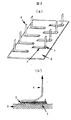
本発明に係る上記電極構造として、十分な接続強度を得るために、図1および図2に示すように、リードからなる電極1の表面にSn−Bi系層2を施すようにした。そして、次に、本発明に係る電極構造の選定について説明する。この選定は、上記要求に基づいて、主に接続強度、ぬれ性、ウィスカー性の評価により行った。
In order to obtain sufficient connection strength as the electrode structure according to the present invention, as shown in FIGS. 1 and 2, a Sn—
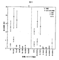
始めにSn−Ag−Bi系はんだと各種電極材料との接続強度を調べた結果を示す。図3に測定方法の概略を示したが、従来のSn−10Pb層の代替材料としてPbのない系で可能性があると考えられる材料(Sn、Sn−Bi、Sn−Zn、Sn−Agめっき)を、Fe−Ni系合金(42アロイ)で形成された電極であるリード上に施したモデルリード4を作成した。この他に、従来のSn−10Pbめっきとの組み合わせについても評価を行った。モデルリード4の形状は、幅3mm、長さ38mmであり、はんだ付け部の長さが22mmになるように直角に折り曲げてある。めっき厚みは各組成ともに約10μmとした。このモデルリード4を82.2重量%Snー2.8重量%Agー15重量%Bi(以下Sn−2.8Ag−15Biと略す)のPbフリーはんだ5を用いて、回路基板であるガラスエポキシ基板6上のCuパッド(Cu電極)7にはんだ付けした。ガラスエポキシ基板6のCuパッド(Cu電極)7の大きさは3.5mm×25mmであり、はんだ5は0.1mm×25mm×3.5mmのはんだ箔で供給した。即ち、ガラスエポキシ基板6上のCuパッド7へ、上記のはんだ箔5を載せ、この上に上記の直角に折り曲げたモデルリード4を載せた。はんだ付けは大気中で、予熱を140℃60秒、最高温度220℃の条件で行った。また、フラックスは、ロジン系で、塩素を含有したフラックスを用いた。はんだ付け後は、有機溶剤で洗浄した。引っ張り試験は、はんだ付け直後と、経時変化による接続部強度劣化を考慮して125℃168時間の高温放置を行ってからと、リードのぬれ性が劣化した場合の界面強度を調べるためにモデルリードを150℃168時間放置してからはんだ付けした場合と3種類行った。引っ張り試験は、基板を固定し、モデルリードの先端をつかんで垂直方向に5mm/分の速度で引っ張った。このときの、最大強度、及び一定となる引張強度を、それぞれフィレット部強度、フラット部強度として各組成のモデルリードについて評価した。この試験は各条件につき10回行い、平均をとった。
First, the results of examining the connection strength between the Sn—Ag—Bi solder and various electrode materials are shown. The outline of the measurement method is shown in FIG. 3, but it is possible to use a Pb-free material (Sn, Sn—Bi, Sn—Zn, Sn—Ag plating) as an alternative material for the conventional Sn-10Pb layer. ) Was made on a lead which is an electrode formed of an Fe—Ni alloy (42 alloy). In addition, the combination with conventional Sn-10Pb plating was also evaluated. The
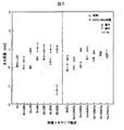
各組成のモデルリードのフィレット部強度の評価結果を図4に示す。通常のQFP−LSI等のプラスチックパッケージ部品ではプリント基板の熱膨張係数の差を考慮すると、フィレット部強度は5kgf程度以上必要である。これから、Sn、及び、Biを23重量%含有しているSn−23Bi以外のSn−Bi系層をFe−Ni系合金(42アロイ)上に施したモデルリードでは、5kgf以上のフィレット部強度が得られたが、Sn−Zn,Sn−Ag,Sn−Pb層の場合では十分な接続界面が得られないことがわかった。この他にも42アロイ上に約2μmのNiめっきを施し、これに、Auめっき、Pdめっき、Pdめっきの上に更にAuめっきを施した3種類のモデルリードを作成し、同様にはんだ付けし、界面強度を調べたが、図4に示したように十分なフィレット部強度が得られなかった。従って、電極であるリード上にSn−Bi系層を施すことが必要であることがわかった。 The evaluation results of the fillet strength of the model lead of each composition are shown in FIG. In general plastic package parts such as QFP-LSI, considering the difference in thermal expansion coefficient of the printed circuit board, the fillet strength needs to be about 5 kgf or more. From this, in the model lead in which the Sn—Bi layer other than Sn-23Bi containing Sn and Bi of 23 wt% is applied on the Fe—Ni alloy (42 alloy), the fillet strength of 5 kgf or more is obtained. Although it was obtained, it was found that a sufficient connection interface could not be obtained in the case of the Sn—Zn, Sn—Ag, Sn—Pb layer. In addition, approximately 2 μm Ni plating is applied on 42 alloy, and then three types of model leads are prepared by Au plating, Pd plating, and Au plating on Pd plating. The interfacial strength was examined, but sufficient fillet strength was not obtained as shown in FIG. Therefore, it has been found that it is necessary to apply a Sn—Bi-based layer on the lead as an electrode.
上記の引っ張り試験を行った各組成のモデルリードのうち、十分な界面強度が得られたSn−Bi系めっきを施したリードについて、Sn−2.8Ag−15Biはんだに対するぬれ性をメニスコグラフ法によって検討した。フラックスは、ぬれ性を調べるため、活性の弱いものを用いた。試験片は上記モデルリードを1cmの長さに切って用いた。ぬれ性の試験条件は、はんだ浴温度が220℃、浸漬速度は1mm/分、浸漬深さは2mm、浸漬時間は20秒とし、荷重が0に回復するまでの時間をぬれ時間、浸漬20秒後の荷重をぬれ荷重とした。また、ぬれ性はめっき直後のリードと、150℃168時間放置したリードについて2種類行った。また、各条件について10回ずつ測定し、平均をとった。 Among the model leads of each composition subjected to the above-described tensile test, the wettability with respect to Sn-2.8Ag-15Bi solder was examined by the meniscograph method for the lead subjected to Sn-Bi plating with sufficient interface strength. did. In order to examine the wettability, a flux with weak activity was used. The test piece was used by cutting the model lead into a length of 1 cm. The test conditions for wettability are as follows: solder bath temperature is 220 ° C., immersion speed is 1 mm / min, immersion depth is 2 mm, immersion time is 20 seconds, and the time until the load recovers to 0 is wet time, immersion is 20 seconds. The subsequent load was defined as a wetting load. In addition, the wettability was measured in two types for the lead immediately after plating and the lead left at 150 ° C. for 168 hours. Moreover, it measured 10 times for each condition and took the average.
各組成のぬれ時間、ぬれ荷重をそれぞれ図5、6に示した。図5のぬれ時間の結果から、めっき初期のSn−Bi系めっきリードでは、Bi濃度が高い方がぬれ性が良いが、150℃168時間の高温放置を行った場合では、Biが1重量%未満、及び23重量%でぬれ性が劣化することがわかった。Biが1重量%未満の場合は、図6に示したように、ぬれ荷重は確保されていたが、ぬれ時間が劣化していたことから、ぬれにくくなっているといえる。従って、Sn−Bi系層のなかでも、十分なぬれ性を得るためには、Bi量は1〜20重量%であることが望ましいことがわかった。 The wetting time and wetting load of each composition are shown in FIGS. From the results of the wetting time shown in FIG. 5, in the Sn-Bi based plating lead in the initial stage of plating, the higher the Bi concentration, the better the wettability, but when left at a high temperature of 150 ° C. for 168 hours, Bi is 1% by weight. It was found that the wettability deteriorated at less than 23% by weight. When Bi is less than 1% by weight, as shown in FIG. 6, the wetting load was secured, but the wetting time was deteriorated, so it can be said that the wetting is difficult. Therefore, it was found that the Bi content is desirably 1 to 20% by weight in order to obtain sufficient wettability among the Sn-Bi based layers.
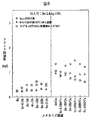
更に熱膨張係数の差が大きい材料間の接続、温度差が大きい環境で使用される場合等では、界面に発生する応力が大きくなるため、十分な信頼性を確保するためには界面の接続強度は10kgf程度以上でなければならない。従って、図4を見てみると、Fe−Ni系合金(42アロイ)に直接Sn−Bi系層を施したのでは、10kgf以上のフィレット部強度が得られないことがわかった。これは、界面での化合物層が十分形成されていないためと考えられる。そこで、界面でのはんだとの反応性を高めるために、Fe−Ni系合金(42アロイ)上に平均7μm程度のCuめっき層、この上にSn−Bi系めっき層を施し界面強度の測定を行った。この時のフィレット部強度の結果をCu層がない場合も合わせて図7に示したが、Bi量が23重量%の場合を除けば、10kgf以上の接続強度が得られ、下地のCu層の効果が確認できた。また、この電極構造を取ることにより、図7に一緒に示したように、Sn−Pb共晶はんだを42アロイリード上に直接Sn−10Pb層を施したリードにはんだ付けした従来の場合に得られるはんだ付け直後の界面強度、12.1kgfと同程度以上の界面強度を得ることができた。また、図8に示したように、Sn−Bi層の下にCu層を施すことによりフラット部強度も向上させることができた。ここで、このCu層は42アロイのリードフレームを用いた場合には、上記のように42アロイ上にCu層を施せばよいが、Cu系リードフレームを用いた場合は、これをこのままCu層としても良いし、また、剛性を向上させるために他の元素をリードフレーム材料中に添加することもあるので、この影響をなくすために、更にCu層を形成してもよい。また、このCu層を施したモデルリードのぬれ性については、図5、6に一緒に示したが、Cu層の影響はほとんど無く、やはりBiが1重量%以下では、高温放置を行った場合にぬれ性が劣化していたが、1〜20重量%では、十分なぬれ性を得ることができた。尚、図7、図8の例はSn−2.8Ag−15Biを用いたが、Bi量が少ない系、例えばSn−2Ag−7.5Bi−0.5Cu系でも、下地にCu層を入れることにより、界面強度向上の効果がある。 In addition, when connecting between materials with a large difference in thermal expansion coefficient or when used in an environment with a large temperature difference, the stress generated at the interface increases, so the interface connection strength is sufficient to ensure sufficient reliability. Must be about 10 kgf or more. Therefore, when FIG. 4 was seen, when the Sn-Bi type | system | group layer was directly given to the Fe-Ni type alloy (42 alloy), it turned out that the fillet part intensity | strength of 10 kgf or more cannot be obtained. This is presumably because the compound layer at the interface is not sufficiently formed. Therefore, in order to increase the reactivity with the solder at the interface, a Cu plating layer having an average of about 7 μm is applied on the Fe—Ni alloy (42 alloy), and an Sn—Bi plating layer is applied thereon to measure the interface strength. went. The result of the fillet strength at this time is shown in FIG. 7 in the case where there is no Cu layer. Except for the case where the Bi amount is 23% by weight, a connection strength of 10 kgf or more can be obtained. The effect was confirmed. Further, by adopting this electrode structure, as shown together in FIG. 7, it is obtained in the conventional case where the Sn—Pb eutectic solder is soldered to the lead having the Sn-10Pb layer directly on the 42 alloy lead. Interfacial strength immediately after soldering was obtained, and an interfacial strength equal to or higher than 12.1 kgf could be obtained. Moreover, as shown in FIG. 8, the strength of the flat portion could be improved by applying a Cu layer under the Sn—Bi layer. Here, when a 42 alloy lead frame is used, the Cu layer may be formed on the 42 alloy as described above. However, when a Cu-based lead frame is used, the Cu layer is used as it is. In addition, other elements may be added to the lead frame material in order to improve the rigidity. Therefore, in order to eliminate this influence, a Cu layer may be further formed. The wettability of the model lead with the Cu layer is shown in FIGS. 5 and 6 together, but there is almost no influence of the Cu layer. When Bi is 1% by weight or less, it is left at high temperature. Although wettability deteriorated, sufficient wettability could be obtained at 1 to 20% by weight. 7 and 8 used Sn-2.8Ag-15Bi. However, even in a system with a small amount of Bi, for example, a Sn-2Ag-7.5Bi-0.5Cu system, a Cu layer is put on the base. Thus, there is an effect of improving the interface strength.
上記のSn−Bi系層、Cu層は、めっきに限らず、ディップ、蒸着、ローラーコート、金属粉末による塗布によって形成することができる。 Said Sn-Bi type | system | group layer and Cu layer can be formed not only by plating but by the application | coating by a dip, vapor deposition, roller coating, and metal powder.
このように、電極材料により異なる理由を調べるために、接続部の断面研磨を行って、界面の様子を調べた。また、引っ張り試験を行った試料の剥離面をSEMで観察した。この代表的な組み合わせについての結果を説明する。
まず、従来使用されているFe−Ni系合金(42アロイ)に直接Sn−10Pbめっきが施されているリードをSn−Ag−Bi系はんだで接合した場合の観察結果を図9に示したが、この組み合わせでは界面にはPbとBiが化合物を作って集まっていて、剥離は42アロイとはんだとの界面で起こっていた。また、剥離したリードの42アロイ表面には、薄くSnが検出され、はんだ中のSnがリードの42アロイと化合物を形成していたと考えられる。従って、上記のPbとBiの化合物が界面に集まることによって、Snと42アロイとの接続面積が小さくなり、接続強度が非常に弱くなったと考えられる。
次に、Sn−10PbめっきをSn−4Biめっきに変えた場合の観察結果を図10に示したが、界面に形成される化合物層は薄く、剥離は同様に42アロイとはんだとの界面で起こっていた。しかし、Biは粒状の結晶のままで、Snと42アロイとの接続面積の低下をSn−10Pbの場合ほど起こさないため、5kgf以上の接続強度を得ることができたと考えられる。この時の化合物層はオージェ分析から、約70nmのSn−Fe層であった。
更にSn−4Bi層の下にCu層を施した場合の観察結果を図11に示したが、界面には、厚いCuとSnの化合物層が形成されることがわかった。剥離は、この化合物層とはんだとの界面、または化合物層中で起こっていた。剥離面は、図10の42アロイリードに直接Sn−Bi層を形成したリードの場合はほとんど平らであったのに比べて、Cu層が存在する場合にはでこぼこしていた。このため、このような剥離面の違いが界面強度の向上につながったと考えられる。
尚、以上の検討結果はSn−Ag−Bi系はんだの別の組成でも同様の結果が得られた。
上記の各組成のモデルリードについて、ウィスカーの発生を調べたが、Sn−Znめっきを施したモデルリードでは表面にウィスカーの発生が見られた。また、Snめっきについては従来からウィスカー性に問題があると言われている。しかし、Sn−Bi系層についてはウィスカーの発生は見られず、耐ウィスカー性も問題なかった。
従って、本発明の電極構造であれば、Sn−Ag−Bi系はんだに対して、接続強度、ぬれ性、耐イスカー性に優れる接続部を得ることができる。
Thus, in order to investigate the reason for the difference depending on the electrode material, the cross section of the connecting portion was polished to examine the state of the interface. Further, the peeled surface of the sample subjected to the tensile test was observed with an SEM. The result about this representative combination will be described.
First, FIG. 9 shows an observation result in the case where a lead in which Sn-10Pb plating is directly applied to a conventionally used Fe—Ni alloy (42 alloy) is joined with Sn—Ag—Bi solder. In this combination, Pb and Bi were collected by forming a compound at the interface, and peeling occurred at the interface between 42 alloy and solder. Further, Sn was thinly detected on the 42 alloy surface of the peeled lead, and it is considered that Sn in the solder formed a compound with the 42 alloy of the lead. Therefore, it is considered that the connection area between Sn and 42 alloy is reduced by the above-mentioned Pb and Bi compounds gathering at the interface, and the connection strength is very weak.
Next, the observation results when Sn-10Pb plating is changed to Sn-4Bi plating are shown in FIG. 10, but the compound layer formed at the interface is thin, and peeling occurs at the interface between 42 alloy and solder as well. It was. However, since Bi remains as a granular crystal and does not cause a decrease in the connection area between Sn and 42 alloy as in the case of Sn-10Pb, it is considered that a connection strength of 5 kgf or more could be obtained. The compound layer at this time was a Sn—Fe layer of about 70 nm based on Auger analysis.
Further, FIG. 11 shows the observation result when the Cu layer is applied under the Sn-4Bi layer, and it was found that a thick Cu and Sn compound layer was formed at the interface. Peeling occurred at the interface between the compound layer and the solder or at the compound layer. The peeling surface was almost flat when the Sn-Bi layer was formed directly on the 42 alloy lead shown in FIG. 10, but it was bumpy when the Cu layer was present. For this reason, it is considered that such a difference in peeled surface led to an improvement in interface strength.
In addition, the same result was obtained with the other examination composition of the Sn-Ag-Bi based solder.
The generation of whiskers was examined for the model leads having the respective compositions described above. Whisker generation was observed on the surface of the model leads subjected to Sn—Zn plating. In addition, Sn plating is conventionally said to have a problem in whisker properties. However, no whisker was observed in the Sn—Bi-based layer, and the whisker resistance was not a problem.
Therefore, with the electrode structure of the present invention, it is possible to obtain a connection portion excellent in connection strength, wettability, and isker resistance with respect to Sn—Ag—Bi solder.
はんだ材料について、主成分がSnで、Biが5〜25重量%、Agが1.5〜3重量%、Cuが0〜1重量%含有するSn−Ag−Bi系はんだを選んだのは、この範囲内の組成のはんだは、220〜240℃ではんだ付けが可能であり、Cuに対して従来実績のあるSn−Ag共晶とほぼ同等のぬれ性を有し、且つ、高温で十分な信頼性を有しているからである。即ち、Sn−Ag−Bi系はんだではBiが約10重量%以上で138℃付近で溶融する部分(3元共晶)を有し高温での信頼性に影響を及ぼすことが心配されるが、この3元共晶析出量を実用上問題のないレベルに抑え、且つ125℃での高温強度も確保している。従って、この組成のはんだを用いて、上記の電極をはんだ付けすることによって、実用的であり、高信頼な電子機器を得ることができる。 About the solder material, the Sn-Ag-Bi based solder containing Sn as the main component, containing 5 to 25% by weight of Bi, 1.5 to 3% by weight of Ag, and 0 to 1% by weight of Cu was selected. Solder having a composition within this range can be soldered at 220 to 240 ° C., has substantially the same wettability as Cu—a conventional Sn—Ag eutectic with Cu, and is sufficient at high temperatures. This is because it has reliability. That is, in the Sn-Ag-Bi based solder, there is a concern that Bi is about 10% by weight or more and has a part (ternary eutectic) that melts at around 138 ° C., which affects reliability at high temperatures. The amount of ternary eutectic precipitation is suppressed to a level where there is no practical problem, and high-temperature strength at 125 ° C. is secured. Therefore, a practical and highly reliable electronic device can be obtained by soldering the above-described electrode using the solder having this composition.
図1にQFP−LSI用のリードの断面構造を示した。これは、リードの断面構造のある一部分を示したものであるが、Fe−Ni系合金(42アロイ)の電極であるリード1上にSn−Bi系層2が形成されている。このSn−Bi系層2はめっきによって形成し、厚みは10μm程度とした。また、Sn−Biめっき層中のBi濃度は8重量%とした。この電極構造を持つ上記のQFP−LSIをSn−2.8Ag−15Biー0.5Cuはんだを用いて回路基板であるガラスエポキシ基板にはんだ付けした。はんだ付けは最高温度を220℃として、窒素リフロー炉を用いて行った。これにより、十分な接続強度を有する接続部を得ることができた。また、同様にSn−2Ag−7.5Biー0.5Cuはんだを用いてガラスエポキシ基板に240℃で大気中でリフローした。リフローした継手は特に高温での信頼性が高い。
FIG. 1 shows a cross-sectional structure of a QFP-LSI lead. This shows a part of the cross-sectional structure of the lead, but the Sn—
図2にTSOP用のリードの断面構造を示した。これも、リードの断面構造のある一部分を示したものであるが、Fe−Ni系合金(42アロイ)の電極であるリード1上にCu層3、その上にSn−Bi系層2が形成されている。このCu層3、Sn−Bi系層2はめっきによって形成した。Cu層3の厚みは8μm程度であり、Sn−Bi系めっき層2の厚みは10μm程度とした。また、Sn−Biめっき層中のBi量は5重量%である。TSOPはリードの剛性が大きいため、実稼働時の部品自身の発熱、また、高温で使用される場合、界面に発生する応力がQFP−LSIと比較して大きくなる。このような場合には、この界面応力に耐えられるように十分な界面強度を有する界面を形成させる必要があり、Sn−Bi系層2の下にCu層3が効果的である。
このTSOPをプリント基板にSn−Ag−Bi系はんだを用いてベーパーリフロー炉ではんだ付けし、温度サイクル試験を行った。試験条件はー55℃30分、125℃30分の1時間/1サイクル、及び、0℃30分、90℃30分の1時間/1サイクルの2条件であり、500サイクル、1000サイクル後に断面観察を行ってクラックの発生状況を調べた。これを、42アロイリード上に直接Sn-10Pb層が形成されているリードを有する同じ大きさのTSOPをSn−Pb共晶はんだではんだ付けした場合と比較したが、ー55℃/125℃の温度サイクルではクラックの発生が早かったが、0℃/90℃の温度サイクルでは、特に問題とはならず、実用上十分な接続界面が得られた。
FIG. 2 shows a cross-sectional structure of a TSOP lead. This also shows a part of the cross-sectional structure of the lead, but the
This TSOP was soldered to a printed board using a Sn-Ag-Bi solder in a vapor reflow furnace, and a temperature cycle test was performed. The test conditions are -55 ° C for 30 minutes, 125 ° C for 30 minutes / hour / cycle, and 0 ° C for 30 minutes, 90 ° C for 30 minutes / hour / cycle. Observation was made to investigate the occurrence of cracks. This was compared with the case where TSOP of the same size having a lead in which a Sn-10Pb layer was directly formed on 42 alloy lead was soldered with Sn—Pb eutectic solder. Although cracking occurred early in the temperature cycle, there was no particular problem in the temperature cycle of 0 ° C./90° C., and a practically sufficient connection interface was obtained.
本発明の電極構成は基板上の電極にも適用することができる。例えば、基板のはんだ付け性を向上させるためにはんだコートが効果的であるが、従来はSn−Pbはんだ、特にSn−Pb共晶はんだ等のPbを含んだはんだを使用している。このため、コート用はんだのPbフリー化として、本発明のSn−Bi層を用いることができる。また、通常、基板の電極はCuで形成されているため、Sn−Ag−Bi系はんだを使用した場合に十分な接続強度を得ることができる。この構成を適用した例を示すが、回路基板であるガラスエポキシ基板上のCuパッド(Cu電極)に約5μm程度のSn−8Bi層をローラーコートで作成した。このはんだ層を形成したために基板に対するぬれ性が向上し、且つ、接続強度も向上させることができた。 The electrode configuration of the present invention can also be applied to electrodes on a substrate. For example, a solder coat is effective for improving the solderability of the substrate, but conventionally, a Sn-Pb solder, particularly a solder containing Pb such as Sn-Pb eutectic solder is used. For this reason, the Sn—Bi layer of the present invention can be used as a Pb-free solder for coating. Moreover, since the electrode of a board | substrate is normally formed with Cu, when Sn-Ag-Bi type solder is used, sufficient connection strength can be obtained. Although an example in which this configuration is applied is shown, a Sn-8Bi layer of about 5 μm was formed by roller coating on a Cu pad (Cu electrode) on a glass epoxy substrate as a circuit board. Since this solder layer was formed, the wettability to the substrate was improved and the connection strength was also improved.
1…Fe−Ni合金のリード(電極)、2…Sn−Bi系層、3…Cu層、4…モデルリード、5…はんだ、6…ガラスエポキシ基板、7…Cuパッド(Cu電極)
DESCRIPTION OF
Claims (11)
前記半導体装置の電極をCu系部材で形成する工程と、Forming an electrode of the semiconductor device with a Cu-based member;
前記Cu系部材で形成された電極上にSn-(1〜20)重量%(ただし、4重量%以上15重量%以下の範囲を除く)Bi系層を設ける工程とを有する半導体装置の製造方法。And a step of providing a Sn- (1-20)% by weight (excluding the range of 4% by weight to 15% by weight) Bi-based layer on the electrode formed of the Cu-based member. .
前記電極上にSn-(1〜20)重量%(ただし、4重量%以上15重量%以下の範囲を除く)Bi系層を設ける工程では、前記Sn-(1〜20)重量%(ただし、4重量%以上15重量%以下の範囲を除く)Bi系層を1層形成することを特徴とする半導体装置の製造方法。In the step of providing a Bi-based layer on the electrode, Sn- (1-20) wt% (excluding the range of 4 wt% to 15 wt%), the Sn- (1-20) wt% (however, A method of manufacturing a semiconductor device, comprising forming one Bi-based layer (excluding a range of 4 wt% to 15 wt%).
前記電極上にSn-(1〜20)重量%(ただし、4重量%以上15重量%以下の範囲を除く)Bi系層を設ける工程では、前記Sn-(1〜20)重量%(ただし、4重量%以上15重量%以下の範囲を除く)Bi系層を前記電極に直接形成することを特徴とする半導体装置の製造方法。In the step of providing a Bi-based layer on the electrode, Sn- (1-20) wt% (excluding the range of 4 wt% to 15 wt%), the Sn- (1-20) wt% (however, A method of manufacturing a semiconductor device, wherein a Bi-based layer is formed directly on the electrode (except for a range of 4 wt% to 15 wt%).
前記電極上にSn-(1〜20)重量%(ただし、4重量%以上15重量%以下の範囲を除く)Bi系層を設ける工程では、前記電極上にCu層を設けた後、前記Cu層上に前記Sn-(1〜20)重量%(ただし、4重量%以上15重量%以下の範囲を除く)Bi系層を設けることを特徴とする半導体装置の製造方法。In the step of providing a Sn- (1-20) wt% (excluding the range of 4 wt% to 15 wt%) Bi-based layer on the electrode, after providing a Cu layer on the electrode, the Cu A method of manufacturing a semiconductor device, comprising: providing a Sn- (1 to 20) wt% (excluding a range of 4 wt% to 15 wt%) Bi-based layer on a layer.
前記半導体装置の電極をFe-Ni系部材で形成する工程と、Forming an electrode of the semiconductor device with an Fe-Ni-based member;
前記Fe-Ni系部材で形成された電極上にSn-(1〜20)重量%(ただし、4重量%以上15重量%以下の範囲を除く)Bi系層を設ける工程とを有する半導体装置の製造方法A step of providing a Sn- (1-20) wt% (excluding the range of 4 wt% or more and 15 wt% or less) Bi-based layer on an electrode formed of the Fe-Ni-based member. Production method
前記電極をFe-Ni系部材で形成する工程では、前記Fe-Ni系部材は42アロイにより形成されることを特徴とする半導体装置の製造方法。In the step of forming the electrode with an Fe—Ni-based member, the Fe—Ni-based member is formed of 42 alloy.
前記電極上にSn-(1〜20)重量%(ただし、4重量%以上15重量%以下の範囲を除く)Bi系層を設ける工程では、前記Sn-(1〜20)重量%(ただし、4重量%以上15重量%以下の範囲を除く)Bi系層を1層形成することを特徴とする半導体装置の製造方法。In the step of providing a Bi-based layer on the electrode, Sn- (1-20) wt% (excluding the range of 4 wt% to 15 wt%), the Sn- (1-20) wt% (however, A method of manufacturing a semiconductor device, comprising forming one Bi-based layer (excluding a range of 4 wt% to 15 wt%).
前記電極上にSn-(1〜20)重量%(ただし、4重量%以上15重量%以下の範囲を除く)Bi系層を設ける工程では、前記Sn-(1〜20)重量%(ただし、4重量%以上15重量%以下の範囲を除く)Bi系層を前記電極に直接形成することを特徴とする半導体装置の製造方法。In the step of providing a Bi-based layer on the electrode, Sn- (1-20) wt% (excluding the range of 4 wt% to 15 wt%), the Sn- (1-20) wt% (however, A method of manufacturing a semiconductor device, wherein a Bi-based layer is formed directly on the electrode (except for a range of 4 wt% to 15 wt%).
前記電極上にSn-(1〜20)重量%(ただし、4重量%以上15重量%以下の範囲を除く)Bi系層を設ける工程では、前記電極上にCu層を設けた後、前記Cu層上に前記Sn-(1〜20)重量%(ただし、4重量%以上15重量%以下の範囲を除く)Bi系層を設けることを特徴とする半導体装置の製造方法。In the step of providing a Sn- (1-20) wt% (excluding the range of 4 wt% to 15 wt%) Bi-based layer on the electrode, after providing a Cu layer on the electrode, the Cu A method of manufacturing a semiconductor device, comprising: providing a Sn- (1 to 20) wt% (excluding a range of 4 wt% to 15 wt%) Bi-based layer on a layer.
前記Sn-(1〜20)重量%(ただし、4重量%以上15重量%以下の範囲を除く)Bi系層はめっきにより設けることを特徴とする半導体装置の製造方法。A manufacturing method of a semiconductor device, wherein the Sn- (1 to 20) wt% (excluding the range of 4 wt% to 15 wt%) Bi-based layer is provided by plating.
前記Sn-(1〜20)重量%(ただし、4重量%以上15重量%以下の範囲を除く)Bi系層はディップ又は蒸着又はローラーコート又は金属粉末の塗布により形成することを特徴とする半導体装置の製造方法。The Sn- (1-20)% by weight (excluding the range of 4% to 15% by weight) Bi-based layer is formed by dipping, vapor deposition, roller coating or metal powder coating. Device manufacturing method.
Priority Applications (1)
| Application Number | Priority Date | Filing Date | Title |
|---|---|---|---|
| JP2004158626A JP4535429B2 (en) | 2004-05-28 | 2004-05-28 | Manufacturing method of semiconductor device |
Applications Claiming Priority (1)
| Application Number | Priority Date | Filing Date | Title |
|---|---|---|---|
| JP2004158626A JP4535429B2 (en) | 2004-05-28 | 2004-05-28 | Manufacturing method of semiconductor device |
Related Parent Applications (1)
| Application Number | Title | Priority Date | Filing Date |
|---|---|---|---|
| JP34681197A Division JP3622462B2 (en) | 1997-12-16 | 1997-12-16 | Semiconductor device |
Related Child Applications (1)
| Application Number | Title | Priority Date | Filing Date |
|---|---|---|---|
| JP2007278307A Division JP4535464B2 (en) | 2007-10-26 | 2007-10-26 | Manufacturing method of electronic equipment |
Publications (3)
| Publication Number | Publication Date |
|---|---|
| JP2004322213A JP2004322213A (en) | 2004-11-18 |
| JP2004322213A5 JP2004322213A5 (en) | 2005-06-30 |
| JP4535429B2 true JP4535429B2 (en) | 2010-09-01 |
Family
ID=33509269
Family Applications (1)
| Application Number | Title | Priority Date | Filing Date |
|---|---|---|---|
| JP2004158626A Expired - Lifetime JP4535429B2 (en) | 2004-05-28 | 2004-05-28 | Manufacturing method of semiconductor device |
Country Status (1)
| Country | Link |
|---|---|
| JP (1) | JP4535429B2 (en) |
Cited By (1)
| Publication number | Priority date | Publication date | Assignee | Title |
|---|---|---|---|---|
| JP2009302568A (en) * | 2009-09-17 | 2009-12-24 | Renesas Technology Corp | Production process of semiconductor devices, and production process of electronic devices |
Citations (3)
| Publication number | Priority date | Publication date | Assignee | Title |
|---|---|---|---|---|
| JPH1041621A (en) * | 1996-07-18 | 1998-02-13 | Fujitsu Ltd | Junction method using tin-bismuth solder |
| JPH1093004A (en) * | 1996-09-11 | 1998-04-10 | Matsushita Electron Corp | Electronic component and manufacture thereof |
| JPH111793A (en) * | 1997-01-28 | 1999-01-06 | Furukawa Electric Co Ltd:The | Reflow solder plating material and its manufacture |
-
2004
- 2004-05-28 JP JP2004158626A patent/JP4535429B2/en not_active Expired - Lifetime
Patent Citations (3)
| Publication number | Priority date | Publication date | Assignee | Title |
|---|---|---|---|---|
| JPH1041621A (en) * | 1996-07-18 | 1998-02-13 | Fujitsu Ltd | Junction method using tin-bismuth solder |
| JPH1093004A (en) * | 1996-09-11 | 1998-04-10 | Matsushita Electron Corp | Electronic component and manufacture thereof |
| JPH111793A (en) * | 1997-01-28 | 1999-01-06 | Furukawa Electric Co Ltd:The | Reflow solder plating material and its manufacture |
Cited By (1)
| Publication number | Priority date | Publication date | Assignee | Title |
|---|---|---|---|---|
| JP2009302568A (en) * | 2009-09-17 | 2009-12-24 | Renesas Technology Corp | Production process of semiconductor devices, and production process of electronic devices |
Also Published As
| Publication number | Publication date |
|---|---|
| JP2004322213A (en) | 2004-11-18 |
Similar Documents
| Publication | Publication Date | Title |
|---|---|---|
| JP3622462B2 (en) | Semiconductor device | |
| TWI392750B (en) | Lead-free solder alloy | |
| JP3446517B2 (en) | Pb-free solder material and electronic equipment using the same | |
| JP2003290974A (en) | Joining structure of electronic circuit device and electronic parts used for the same | |
| JP4535429B2 (en) | Manufacturing method of semiconductor device | |
| US20020009610A1 (en) | Technical field | |
| JP3551168B2 (en) | Pb-free solder connection structure and electronic equipment | |
| JP5061168B2 (en) | Manufacturing method of electronic equipment | |
| JP3551167B2 (en) | Semiconductor device | |
| JP4535464B2 (en) | Manufacturing method of electronic equipment | |
| JP3551169B2 (en) | Electronic device and method of manufacturing the same | |
| CA2493351C (en) | Pb-free solder-connected structure and electronic device | |
| JP3460442B2 (en) | Lead-free solder and mounted products using it | |
| JP2003200288A (en) | Pb-FREE SOLDER MATERIAL AND ELECTRONIC APPARATUS USING THE SAME |
Legal Events
| Date | Code | Title | Description |
|---|---|---|---|
| A521 | Written amendment |
Free format text: JAPANESE INTERMEDIATE CODE: A523 Effective date: 20041216 |
|
| A621 | Written request for application examination |
Free format text: JAPANESE INTERMEDIATE CODE: A621 Effective date: 20041216 |
|
| RD01 | Notification of change of attorney |
Free format text: JAPANESE INTERMEDIATE CODE: A7421 Effective date: 20060421 |
|
| A131 | Notification of reasons for refusal |
Free format text: JAPANESE INTERMEDIATE CODE: A131 Effective date: 20070828 |
|
| A521 | Written amendment |
Free format text: JAPANESE INTERMEDIATE CODE: A523 Effective date: 20071026 |
|
| A131 | Notification of reasons for refusal |
Free format text: JAPANESE INTERMEDIATE CODE: A131 Effective date: 20080520 |
|
| A521 | Written amendment |
Free format text: JAPANESE INTERMEDIATE CODE: A523 Effective date: 20080722 |
|
| A711 | Notification of change in applicant |
Free format text: JAPANESE INTERMEDIATE CODE: A711 Effective date: 20090227 |
|
| A521 | Written amendment |
Free format text: JAPANESE INTERMEDIATE CODE: A821 Effective date: 20090227 |
|
| A131 | Notification of reasons for refusal |
Free format text: JAPANESE INTERMEDIATE CODE: A131 Effective date: 20090721 |
|
| A521 | Written amendment |
Free format text: JAPANESE INTERMEDIATE CODE: A523 Effective date: 20090917 |
|
| TRDD | Decision of grant or rejection written | ||
| A01 | Written decision to grant a patent or to grant a registration (utility model) |
Free format text: JAPANESE INTERMEDIATE CODE: A01 Effective date: 20100525 |
|
| A01 | Written decision to grant a patent or to grant a registration (utility model) |
Free format text: JAPANESE INTERMEDIATE CODE: A01 |
|
| A711 | Notification of change in applicant |
Free format text: JAPANESE INTERMEDIATE CODE: A712 Effective date: 20100528 |
|
| A61 | First payment of annual fees (during grant procedure) |
Free format text: JAPANESE INTERMEDIATE CODE: A61 Effective date: 20100611 |
|
| FPAY | Renewal fee payment (event date is renewal date of database) |
Free format text: PAYMENT UNTIL: 20130625 Year of fee payment: 3 |
|
| R150 | Certificate of patent or registration of utility model |
Free format text: JAPANESE INTERMEDIATE CODE: R150 |
|
| FPAY | Renewal fee payment (event date is renewal date of database) |
Free format text: PAYMENT UNTIL: 20130625 Year of fee payment: 3 |
|
| FPAY | Renewal fee payment (event date is renewal date of database) |
Free format text: PAYMENT UNTIL: 20140625 Year of fee payment: 4 |
|
| S531 | Written request for registration of change of domicile |
Free format text: JAPANESE INTERMEDIATE CODE: R313531 |
|
| R350 | Written notification of registration of transfer |
Free format text: JAPANESE INTERMEDIATE CODE: R350 |
|
| EXPY | Cancellation because of completion of term |