JP4532002B2 - Solder resist ink - Google Patents
Solder resist ink Download PDFInfo
- Publication number
- JP4532002B2 JP4532002B2 JP2001058254A JP2001058254A JP4532002B2 JP 4532002 B2 JP4532002 B2 JP 4532002B2 JP 2001058254 A JP2001058254 A JP 2001058254A JP 2001058254 A JP2001058254 A JP 2001058254A JP 4532002 B2 JP4532002 B2 JP 4532002B2
- Authority
- JP
- Japan
- Prior art keywords
- solder resist
- resist ink
- pigment
- halogen
- ultraviolet curable
- Prior art date
- Legal status (The legal status is an assumption and is not a legal conclusion. Google has not performed a legal analysis and makes no representation as to the accuracy of the status listed.)
- Expired - Fee Related
Links
Description
【0001】
【発明の属する技術分野】
本発明は、プリント配線板の永久保護膜を形成するためのソルダーレジストインクに関する。更に詳しくは、本発明は紫外線照射により硬化するソルダーレジストインクに関する。
特に本発明は、希アルカリ水溶液で現像可能なフォトソルダーレジストインクと、非現像タイプの紫外線硬化型ソルダーレジストに関する。このソルダーレジストンクは、燃焼時における有毒ガス発生量が著しく低減化されている。
【0002】
【従来の技術】
電気製品において使用されているプリント配線基板は、銅張積層板などの基板上に所定の配線が形成されたものである。このプリント配線基板はソルダリングの際における不要な部分へのはんだの付着を防止して、電気的短絡を回避等するとともに、その寿命の短縮化を防止するために、基板上に導体配線を形成した後、ソルダーレジストインクの硬化物から成る永久保護膜が所定パターンで形成されるのが一般的である。
このようなプリント配線基板を構成する基板やソルダーレジストインクには、従来、臭化物等のハロゲン化物が含まれており、その燃焼時に有毒ガスが発生する場合があり、問題となっていた。
【0003】
しかしながら、近年における環境問題や人体に対する安全性への関心の高まりに伴って燃焼時に有毒ガスを発生しないプリント配線基板の開発が求められている。このような要求に応えて、例えば脱ハロゲン化されたガラスエポキシ銅張積層板等の基板が開発されているが、ソルダーレジストインクに関しては、十分なハロゲン含有量の低減化を達成するには至っていない。
【0004】
一般的に、プリント配線基板上において形成されたソルダーレジストインクの永久保護膜は、目視検査時における視認性に優れ、しかも目に優しいことが必要であり、そのためにこの永久保護膜は緑色を呈していることが要求される。
そこで、従来のソルダーレジストインクは、フタロシアニングリーン等の着色顔料が配合されていて、緑色を呈するようになっていた。しかしながら、このフタロシアニングリーンは、その化学構造式中に塩素や臭素を高比率で含んでいる。
具体的に示すと、例えばカラーインデックスがピグメントグリーン7であるフタロシアニングリーンは1分子中に約47重量%の塩素を含んでおり、またピグメントグリーン36であるフタロシアニングリーンは1分子中に約5重量%の塩素と約60重量%の臭素を含んでいる。
従って、フタロシアニングリーンのようなハロゲンを高比率で含む着色顔料を配合して成る従来のソルダーレジストインクは、その燃焼時に、多量の有毒ガスを発生してしまう。
【0005】
【発明が解決しようとする課題】
そこで、本発明は、ハロゲンを含有しない、またはハロゲン含有量が著しく低減化されたソルダーレジストインクを提供することを課題とする。
【0006】
【課題を解決するための手段】
本願第一の発明は、
(A)紫外線硬化性成分、
(B)光重合開始剤、および
(C)化学構造式中にハロゲンを含まない黄色顔料と化学構造式中にハロゲンを含まない黒色顔料とからなり緑色を呈するように配合された着色顔料を含むことを特徴とするソルダーレジストインクである。
【0007】
また、本願第二の発明は
(A−1)側鎖にエチレン性不飽和基とカルボキシル基とを有する紫外線硬化性樹脂、
(B)光重合開始剤、および
(C)化学構造式中にハロゲンを含まない黄色顔料と化学構造式中にハロゲンを含まない黒色顔料とからなり緑色を呈するように配合された着色顔料を含むことを特徴とするソルダーレジストインクである。このソルダーレジストインクは、特に、フォトソルダーレジストインクとしての用途を有する。
【0008】
さらに、このフォトソルダーレジストインクの紫外線硬化性成分として、(A−4)エチレン性不飽和単量体を含んでいることが好ましい。
また、このソルダーレジストインクは、さらに(D)有機溶剤を含んでいることが好ましい。
この本願第二の発明のソルダーレジストインクは、(E)多官能エポキシ化合物をさらに含んでいることが好ましい。
また、このソルダーレジストインクの硬化物中のハロゲン含有量は500ppm以下になっていることが好ましい。
また、上記のソルダーレジストキンクにおいて配合される(A−1)成分としての紫外線硬化性樹脂および(E)成分としての多官能エポキシ化合物は、例えば、過酸法によって合成されたハロゲンを含有しないエポキシ化合物、またはハロゲン含有量を低減化するための処理を施したエポキシ化合物から調製されたものであり、このようにして調整された(A−1)成分および/または(E)成分を使用すると、本発明のフォトソルダーレジストインクの硬化物中のハロゲン含有量を150ppm以下にすることができる。
また、その(C)成分としての着色顔料は、重量比1:10〜10:1で配合された黄色顔料および前記黒色顔料であることが好ましい。
【0009】
また、本願第三の発明は、
(Aー3)エポキシ(メタ)アクリレートおよび/または多価フェノールのポリエーテル化物と(メタ)アクリル酸とのエステル化物、
前記(Aー3)成分以外の(A−4)エチレン性不飽和化合物、
(B)光重合開始剤、および
(C)化学構造式中にハロゲンを含まない黄色顔料と化学構造式中にハロゲンを含まない黒色顔料とからなり緑色を呈するように配合された着色顔料を含むことを特徴とするソルダーレジストインクである。このソルダーレジストインクは,特に、紫外線硬化型のソルダーレジストインクとして利用される。
【0010】
この本願第三の発明の紫外線硬化型のソルダーレジストインクの硬化物中のハロゲン含有量は500ppm以下になっていることが好ましい。
また、その着色顔料は、化学構造式中にハロゲンを含まない黄色着色顔料と化学構造式中にハロゲンを含まない黒色着色顔料の重量比1:10〜10:1の組み合わせであることが好ましい。
以下に本発明を更に詳細に説明する。
【0011】
【発明の実施の形態】
本発明のソルダーレジストインクは、(A) 紫外線硬化性成分、(B)光重合開始剤、および(C)化学構造式中にハロゲンを含まない黄色顔料と化学構造式中にハロゲンを含まない黒色顔料を含んでいる。
【0012】
(A)紫外線硬化性成分
本発明のソルダーレジストインクは、(A)成分として紫外線硬化性成分が配合されている。この紫外線硬化性成分は、紫外線硬化性機能を有する成分であり、この紫外線硬化性成分を後述の(C)成分としての光重合開始剤とともに含む本発明のソルダーレジストインクは、紫外線を照射すると硬化する。
【0013】
なお、後述の(D)有機溶剤が含まれる場合にはこの有機溶剤を除く本発明のソルダーレジストインクの全成分中の(A)紫外線硬化性成分は、好ましくは20〜80重量%含まれている。
【0014】
本発明において配合される(A)紫外線硬化性成分は、紫外線照射によって硬化するものであれば特に限定されず、例えば、光反応性の二重結合を有する紫外線硬化性樹脂や光重合性の単量体等の従来周知の紫外線硬化性成分のなかから任意に選択される。
【0015】
(B)光重合開始剤
本発明のソルダーレジストインクには、上記の(A)紫外線硬化性成分に加えて、(B)成分としての光重合開始剤が含まれている。
本発明に含まれる上記の光重合開始剤は、特に限定されないが、本発明に好適な光重合開始剤としては、例えば、ベンゾイン;ベンゾインメチルエーテル、ベンゾインエチルエーテルおよびベンゾインイソプロピルエーテル等のベンゾインのアルキルエーテル類;アセトフェノン、2,2−ジメトキシ−2−フェニルアセトフェノン、2,2−ジエトキシ−2−フェニルアセトフェノン、および1−ヒドロキシシクロヘキシルフェニルケトン等のアセトフェノン類;2−メチルアントラキノン、2−エチルアントラキノンおよび2−アミルアントラキノン等のアントラキノン類;2,4−ジメチルチオキサントン、2,4−ジエチルチオキサントン、および2,4−ジイソプロピルチオキサントン等のチオキサントン類;アセトフェノンジメチルケタールおよびベンジルジメチルケタール等のケタール類;ベンゾフェノン、3,3−ジメチル−4−メトキシベンゾフェノン、3,3' ,4,4' −テトラ−(t−ブチルペルオキシルカルボニル)ベンゾフェノンおよび4−ベンゾイル−4−メチルジフェニルスルフィド等のベンゾフェノン類又はキサントン類;2−ヒドロキシ−2−メチル−1−フェニル−プロパン−1−オンおよび1−ヒドロキシ−シクロヘキシル−フェニル−ケトン等のα−ヒドロキシケトン類;2−メチル−1−[4−(メチルチオ)フェニル]−2−モルフォリノ−プロパン−1−オン、2−ベンゾイル−2−ジメチルアミノ−1−(4−モルフォリノフェニル)−ブタノン−1、4,4’−ビス−ジエチルアミノベンゾフェノン等の窒素原子を含むもの;2,4,6−トリメチルベンゾイルジフェニルホスフィンオキシド等が挙げられる。
これらの(B)光重合開始剤は、本発明のソルダーレジストインクを調製するために、各々単独で又は適宜組み合わせて配合される。
また、これらの光重合開始剤は、安息香酸系、p−ジメチルアミノ安息香酸エチルエステル、p−ジメチルアミノ安息香酸イソアミルエステル、2−ジメチルアミノエチルベンゾエート等の第三級アミン系等の公知の光重合促進剤や増感剤等と併用しても良い。
【0016】
この(B)成分としての光重合開始剤は、後述の(D)有機溶剤が含まれる場合にはこの有機溶剤を除く本発明のソルダーレジストインクの全成分中に、好ましくは0.1〜30重量%、更には0.1〜10重量%、最適には0.1〜7重量%含まれている。上記の範囲の配合量で光重合開始剤が含まれている場合に、本発明のソルダーレジストインクは優れた光硬化性を示し、得られる永久保護膜の物性も良好になる。
【0017】
(C)着色顔料
さらに本発明のソルダーレジストインクには、(C)成分として着色顔料が配合されている。本発明において配合されるこの着色顔料は、化学構造式中にハロゲンを含まない黄色顔料と化学構造式中にハロゲンを含まない黒色顔料とからなるものであり、しかもこれらの黄色顔料および黒色顔料は、得られる本発明のソルダーレジストインクやその硬化皮膜が実質的に緑色を呈するような比率で配合されている。ここで実質的に緑色を呈するような比率とは、ソルダーレジストインクやその硬化被膜が肉眼によって観察された場合に、看者がそれを緑色であると認識できるのに十分な程度の色相や色合いを有するような比率をいう。これによって、本発明のソルダーレジストインクを使用して作製されたプリント配線基板のパターンは、目視検査の際の視認性に優れ、しかも目に優しい。
【0018】
上記(C)成分を構成する化学構造式中にハロゲンを含まない黄色顔料としては、例えばカラーインデックスでC.I.ピグメントイエローとして分類されているものが挙げられる。
また、上記カラーインデックスでC.I.ピグメントイエローのなかでも、特に、カラーインデックス(C.I.)ピグメントイエロー139および185等で示されるイソインドリン系顔料、
カラーインデックス(C.I.)ピグメントイエロー120、151、175、180、181および194等で示されるベンツイミダゾロン系顔料、
カラーインデックス(C.I.)ピグメントイエロー148、182および192等で示される縮合多環系顔料、
カラーインデックス(C.I.)ピグメントイエロー101等で示されるビスアゾメチン系顔料、
カラーインデックス(C.I.)ピグメントイエロー1、4、5、7、9、65、74、150、154および167等で示されるモノアゾ系顔料、
カラーインデックス(C.I.)ピグメントイエロー24、108、123、147および193等で示されるアントラキノン系顔料、
カラーインデックス(C.I.)ピグメントイエロー155等で示されるビスアゾ系顔料、
カラーインデックス(C.I.)ピグメントイエロー117、129、153、177および179等で示される金属錯体系顔料、
カラーインデックス(C.I.)ピグメントイエロー24で示されるフラバントロンイエロー、
カラーインデックス(C.I.)ピグメントイエロー42等で示される酸化鉄系顔料、ならびに
カラーインデックス(C.I.)ピグメントイエロー61、62、100、104、133、168および169等で示されるアゾレーキ系顔料などをが例示される。これらの好適な黄色顔料は、それぞれ単独で、または適宜組み合わて配合される。
【0019】
上記(C)成分を構成する化学構造式中にハロゲンを含まない黒色顔料としては、例えばカラーインデックスでC.I.ピグメントブラックとして分類されているものが例示される。
また、上記のようにして例示されるカラーインデックスでC.I.ピグメントブラックの中でも、特に、カラーインデックス(C.I.)ピグメントブラック6、7、9および18等で示されるカーボンブラック系顔料、
カラーインデックス(C.I.)ピグメントブラック8および10等で示される黒鉛系顔料、
カラーインデックス(C.I.)ピグメントブラック31および32等で示されるペリレン系顔料、
カラーインデックス(C.I.)ピグメントブラック11、12および27等で示される酸化鉄系顔料、
カラーインデックス(C.I.)ピグメントブラック13、25および29等で示される酸化コバルト系顔料、
カラーインデックス(C.I.)ピグメントブラック15および28等で示される酸化銅系顔料、
カラーインデックス(C.I.)ピグメントブラック14および26等で示されるマンガン系顔料、
カラーインデックス(C.I.)ピグメントブラック23等で示される酸化アンチモン系顔料、
カラーインデックス(C.I.)ピグメントブラック30等で示される酸化ニッケル系顔料、
カラーインデックス(C.I.)ピグメントブラック34等で示される顔料が例示される。
また、硫化モリブデン、或いは硫化ビスマス等を例示できる。
これらの好適な黒色顔料は、それぞれ単独で、または適宜組み合わせて使用される。
また、上記の例示される好適な黒色顔料中でも、特にカーボンブラック系顔料や黒鉛系顔料や、カラーインデックス(C.I.)ピグメントブラック31および32等で示されるペリレン系顔料が好ましい。特にこのペリレン系顔料は、400nm以上の領域で反射領域を持っており、このペリレン系顔料を配合してなるフォトソルダーレジストインクは優れた感光性を有している。
【0020】
なお、黄色顔料および黒色顔料は、好ましくは1:10〜10:1、更には1:5〜5:1の重量比で組み合わされていることが好ましい。さらに好ましくは、黄色顔料100重量部に対して黒色顔料10〜30重量部となるような重量比で組み合わされている。黄色顔料および黒色顔料を上記の範囲で組み合わせることによって、得られるソルダーレジストインクまたはその硬化皮膜は実質的に緑色を呈するようになる。なお、本発明のソルダーレジストインク自体の色が必ずしも緑色ではない場合であっても、本発明のソルダーレジストインクの硬化物がブロンズ色の銅張積層板上において緑色になっていればよい。
上記の範囲で配合される黄色顔料と黒色顔料から成る(C)着色顔料は、本発明のソルダーレジストインクの他の成分への分散性が良好であり、かつ、色ムラの少ない鮮やかな緑色の永久保護膜を形成するソルダーレジストインクを得ることができる。
【0021】
また、本発明のソルダーレジストインク中における上記(C)着色顔料の配合量は特に限定されないが、この(C)着色顔料は、(D)有機溶剤が含まれる場合にはこの有機溶剤を除いて、本発明のソルダーレジストンク中に、好ましくは0.01〜20重量%、更には0.1〜10重量%、最適には0.2〜5重量%含まれている。着色顔料の配合量が上記の範囲にある場合において、紫外線透過率の減少による樹脂硬化性の低下を抑制しつつ目視検査時の視認性が良好な永久保護膜を形成できる。
【0022】
なお、従来使用されていたフタロシアニングリーン顔料は、粒子が微細化され難く分散性が比較的悪い。従って、塗膜の表面状態、電気特性や耐湿性等に悪影響を及ぼさないように、ソルダーレジストインクを配合調製する際において長時間の混練工程を必要とした。しかしながら、上記の着色顔料(C)は、フタロシアニングリーンと比較して他の成分中への分散性が良好であり、比較的容易に混練配合されるため、容易に本発明のソルダーレジストインクを調製することができる。
【0023】
(I)フォトソルダーレジストインク
本発明のソルダーレジストインクがフォトソルダーレジストインクとして利用される場合、インクを有機溶剤或いは希アルカリ水溶液等で現像可能なものとすべく紫外線硬化性樹脂を含む。特にこのインクを希アルカリ水溶液で現像可能なものとする場合には、(A)成分としての紫外線硬化性成分は、(A−1)側鎖にエチレン性不飽和基とカルボキシル基とを有する紫外線硬化性樹脂を好適に用いることができる。
特に上記フォトソルダーレジストインクの場合には、(A−1)側鎖にエチレン性不飽和基とカルボキシル基とを有する紫外線硬化性樹脂、(B)光重合開始剤および(C)着色顔料から成ることが好ましい。
【0024】
なお、本発明において、「フォトソルダーレジストインク」とは、いわゆる現像型のソルダーレジストインクをいい、例えば、基板上に塗布されたソルダーレジストインクに紫外線を選択的に露光してこの被露光部分のソルダーレジストインクを硬化し、しかる後に未露光部分のソルダーレジストインクを、例えば希アルカリ水溶液中で洗浄除去して、所定パターンの永久保護膜を得るタイプのソルダーレジストインクが該当する。
【0025】
(A−1) 側鎖にエチレン性不飽和基とカルボキシル基とを有する紫外線硬化性樹脂
本発明のフォトソルダーレジストインクは、(A−1)成分として、側鎖にエチレン性不飽和基とカルボキシル基とを有する紫外線硬化性樹脂が配合されている。この(A−1)成分は、その化学構造式中に光硬化性のエチレン性不飽和基およびカルボキシル基を有しているので、紫外線等の露光によって所定のエネルギーを吸収すると、これによる露光部分は硬化して希アルカリ水溶液に対する分散性や溶解性が低下する。従って、基板に塗布された上記(A−1)成分を含む本発明のフォトソルダーレジストインクを選択的に露光して、露光部分のフォトソルダーレジストインクを硬化させ、その後、この基板を希アルカリ水溶液で洗浄して非露光部分の未硬化のフォトソルダーレジストインクを希アルカリ水溶液によって溶解除去すると、所定パターンが基板上に形成される。
【0026】
ここで、この(A−1)成分の紫外線硬化性樹脂はその化学構造式中に光重合性のエチレン性不飽和基を有している。このような光重合性のエチレン性不飽和基としては、(メタ)アクリロイル基やビニル基等の不飽和基を例示することができる。この光重合性のエチレン性不飽和基の含有量は特に限定されないが、紫外線硬化性樹脂中の不飽和基の含有量は0.01〜10モル/Kg(紫外線硬化性樹脂)、特に好ましくは、0.1〜5モル/Kgになっている。紫外線硬化性樹脂中の不飽和基の含有量が上記のような範囲にある場合に、特に優れた露光感度と現像性とを兼ね備えるフォトソルダーレジストインクを調製することができる。
【0027】
また(A−1)成分としての紫外線硬化性樹脂は、その酸価が30〜200mgKOH/g、特に40〜160mgKOH/gになっていることが好ましい。紫外線硬化性樹脂の酸価が上記の範囲にある場合に、他の成分との相溶性が良好になるとともに、特に良好な露光感度、現像性および解像性を有するフォトソルダーレジストインクを調製することができる。
【0028】
さらに(A−1)成分としての紫外線硬化性樹脂の重量平均分子量は、特に限定されるものではないが、3,000〜400,000、特に5,000〜100,000、最適には5,000〜50,000になっていることが好ましい。紫外線硬化性樹脂の重量平均分子量が上記の範囲にある場合に、本発明のフォトソルダーレジストインクの解像性や露光感度のバランスが特に優れる。
【0029】
上記(A−1)成分としては、例えば、「側鎖にエポキシ基を有するポリマー」中の前記エポキシ基に「カルボキシル基を有するエチレン性不飽和化合物」と「多価カルボン酸無水物」とを付加して成る紫外線硬化性樹脂が挙げられる。
【0030】
上記(A−1)成分として例示される紫外線硬化性樹脂を調製するための「側鎖にエポキシ基を有するポリマー(骨格ポリマー)」としては、次のようなエポキシ化合物とエチレン性不飽和単量体との共重合体が挙げられる。
即ち、上記のエポキシ化合物としては、グリシジル(メタ)アクリレートや2−メチルグリシジル(メタ)アクリレート等のグリシジル(メタ)アクリレート類、および(3,4−エポキシシクロヘキシル)メチル(メタ)アクリレート等の(メタ)アクリル酸のエポキシシクロヘキシル誘導体類等が挙げられる。
また、上記のエチレン性不飽和単量体としては、脂肪族又は脂環族のアルキル(メタ)アクリレート;ベンジル(メタ)アクリレート等の芳香族系(メタ)アクリレート;ヒドロキシエチル(メタ)アクリレートやメトキシエチル(メタ)アクリレート等のエチレングリコールエステル系(メタ)アクリレート、ポリエチレングリコールエステル系(メタ)アクリレートおよびプロピレングリコール系(メタ)アクリレート;(メタ)アクリルアミド系化合物;N−置換マレイミド系化合物;ビニルピロリドン;(メタ)アクリロニトリル;酢酸ビニル;スチレン;α−メチルスチレン;およびビニルエーテル等が挙げられる。
なお、本明細書において、(メタ)アクリル酸とはアクリル酸とメタクリル酸とを総称するものであり、(メタ)アクリレートとはアクリレートとメタクリレートとを総称するものである。
【0031】
また、上記(A−1)成分として例示される紫外線硬化性樹脂を調製するための「側鎖にエポキシ基を有するポリマー(骨格ポリマー)」としては、上記のエポキシ化合物とエチレン性不飽和単量体との共重合体に加えて、例えばフェノールノボラック型エポキシ樹脂、クレゾールノボラック型エポキシ樹脂、ビスフェノールA型エポキシ樹脂、ビスフェノールF型エポキシ樹脂、ビスフェノールA−ノボラック型エポキシ樹脂、脂環式エポキシ樹脂(例えばダイセル化学工業社製「EHPE−3150」)、およびトリス(ヒドロキシフェニル)メタンの誘導体である多官能エポキシ樹脂(例えば、日本化薬(株)製EPPN−502H、およびダウケミカル社製タクテックス−742及びXD−9053等)等のエポキシ樹脂を挙げることができる。
【0032】
また、上記(A−1)成分として例示される紫外線硬化性樹脂を調製するための「カルボキシル基を有するエチレン性不飽和単量体」としては、例えば(メタ)アクリル酸、クロトン酸、桂皮酸、2−(メタ)アクリロイルオキシエチルコハク酸、2−(メタ)アクリロイルオキシエチルフタル酸、β−カルボキシエチルアクリレート、アクリロイルオキシエチルサクシネート、2−プロペノイックアシッド,3−(2−カルボキシエトキシ)−3−オキシプロピルエステル、2−(メタ)アクリロイルオキシエチルテトラヒドロフタル酸および2−(メタ)アクリロイルオキシエチルヘキサヒドロフタル酸等のエチレン性不飽和基を1個有するもの、並びにペンタエリスリトールトリ(メタ)アクリレート、トリメチロールプロパンジ(メタ)アクリレート、ジペンタエリスリトールペンタ(メタ)アクリレート等のヒドロキシル基を有する多官能アクリレートに二塩基酸無水物を反応させて得られるもののようなエチレン性不飽和基を複数有するものが挙げられる。
これらの中でもカルボキシル基を1個有するものが好ましく、特に(メタ)アクリル酸を用いるか、(メタ)アクリル酸を主成分として用いるのが好ましい。(メタ)アクリル酸により導入されるエチレン性不飽和基は光反応性に優れるからである。
これらの「カルボキシル基を有するエチレン性不飽和単量体」はそれぞれ、単独で、または適宜組み合わせて使用できる。
【0033】
また、上記(A−1)成分として例示される紫外線硬化性樹脂を調製するための「多価カルボン酸無水物」としては、例えば、無水コハク酸、無水メチルコハク酸、無水マレイン酸、無水シトラコン酸、無水グルタル酸、無水イタコン酸、無水フタル酸、テトラヒドロ無水フタル酸、メチルテトラヒドロ無水フタル酸、無水メチルナジック酸、ヘキサヒドロ無水フタル酸およびメチルヘキサヒドロ無水フタル酸等の2塩基酸無水物、並びに無水トリメリット酸、無水ピロメリット酸、無水ベンゾフェノンテトラカルボン酸およびメチルシクロヘキセンテトラカルボン酸無水物等の3塩基酸以上の酸無水物が挙げられる。
これらの「多価カルボン酸無水物」はそれぞれ、単独で、または適宜組み合わせて使用できる。
【0034】
上記のような、側鎖にエポキシ基を有するポリマーの前記エポキシ基に、カルボキシル基を有するエチレン性不飽和化合物と多価カルボン酸無水物とを付加して(A−1)成分として例示される紫外線硬化性樹脂を調製するための付加反応は、例えば熱重合禁止剤及び付加触媒の存在下において60〜150℃程度に加熱することによって行われる。
なお、上記の付加反応は、「側鎖にエポキシ基を有するポリマー」に「カルボキシル基を有するエチレン性不飽和化合物」を付加させた後に「多価カルボン酸無水物」を付加させてもよく、また、「側鎖にエポキシ基を有するポリマー」に「多価カルボン酸無水物」を付加させた後に「カルボキシル基を有するエチレン性不飽和化合物」を付加させてもよいが、前者の方が好ましい。
【0035】
後述の有機溶剤を除く本発明のフォトソルダーレジストインクの全成分中における上記(A−1)成分の配合量は、特に限定されないが、好ましくは10〜80重量%、更には20〜70重量%、最適には25〜60重量%になっている。(A−1)成分の配合量が上記の範囲にある場合に、アルカリ現像性、感度および解像性が良好なフォトソルダーレジストインクを得ることができる。
【0036】
(A−4)エチレン性不飽和単量体
また、本発明のフォトソルダーレジストインクは、上記の(A−1)に加えて、さらに(A)紫外線硬化性成分としての(A−4)エチレン性不飽和単量体を配合して、塗布性、耐熱性および絶縁性等の特性を向上させてもよい。また、この(A−4)光重合性エチレン性不飽和単量体は、希釈剤としての役割を果たすとともに、露光感度を調節する役割を果たす。
このようなエチレン性不飽和単量体としては、2−ヒドロキシエチル(メタ)アクリレート、2−ヒドロキシプロピル(メタ)アクリレート、N−ビニルピロリドン、(メタ)アクリロイルモルフォリン、メトキシテトラエチレングリコール(メタ)アクリレート、メトキシポリエチレングリコール(メタ)アクリレート、ポリエチレングリコールジ(メタ)アクリレート、N,N−ジメチル(メタ)アクリルアミド、N−メチロール(メタ)アクリルアミド、N,N−ジメチルアミノプロピル(メタ)アクリルアミド、N,N−ジメチルアミノエチル(メタ)アクリレート、メラミン(メタ)アクリレート、ジエチレングリコールジ(メタ)アクリレート、トリエチレングリコールジ(メタ)アクリレート、プロピレングリコールジ(メタ)アクリレート、フェノキシエチル(メタ)アクリレート、テトラヒドロフルフリル(メタ)アクリレート、シクロヘキシル(メタ)アクリレート、トリメチロールプロパンジ(メタ)アクリレート、トリメチロールプロパントリ(メタ)アクリレート、ペンタエリスリトールトリ(メタ)アクリレート、ペンタエリスリトールテトラ(メタ)アクリレート、ジペンタエリスリトールペンタ(メタ)アクリレート、ジペンタエリスリトールヘキサ(メタ)アクリレート、イソボニル(メタ)アクリレート、シクロペンタニルモノ(メタ)アクリレートおよびシクロペンテニルモノ(メタ)アクリレート;多塩基酸とヒドロキシアルキル(メタ)アクリレートとのモノエステル、ジエステル、トリエステル又はポリエステル;ポリエステル(メタ)アクリレート、ウレタン(メタ)アクリレート等の(メタ)アクリレート単量体等が挙げられる。
これらのエチレン性不飽和単量体は、本発明のフォトソルダーレジストインクを調製するために、それぞれ単独であるいは適宜組み合わされて配合されている。
【0037】
有機溶剤を除くフォトソルダーレジストインクの全成分中の上記(A−4)エチレン性不飽和単量体の配合量は、特に限定されないが、好ましくは1〜50重量%、更には1〜40重量%、最適には1〜30重量%である。上記の範囲の光重合性エチレン性不飽和単量体を配合することによって、乾燥塗膜が適度な表面粘着性を有するとともに、パターンを描いたネガマスクを乾燥塗膜に当てて露光する際のネガマスクの汚損の問題を防止できる。
【0038】
また、本発明のフォトソルダーレジストインクは、必要に応じて、さらに、エポキシ(メタ)アクリレート等の紫外線硬化性高分子、(メタ)アクリル酸エステル共重合体、スチレン−マレイン酸樹脂等のエチレン性不飽和化合物の重合体、或いは、これらにさらにエチレン性不飽和基を導入してなる紫外線硬化性重合体等を配合してもよい。
【0039】
(B)光重合開始剤
本発明のフォトソルダーレジストインクは、さらに(B)成分として光重合開始剤が配合されている。
【0040】
(B)成分としては先に列挙された光重合開始剤が好ましくは使用される。
【0041】
また、有機溶剤を除く本発明のフォトソルダーレジストインクの全成分中における(B)成分としての光重合開始剤は、好ましくは0.1〜30重量%、更には1〜10重量%、最適には1〜7重量%含まれている。上記の範囲の配合量で光重合開始剤が含まれている場合に、本発明のフォトソルダーレジストインクは優れた光硬化性を示し、得られる永久保護膜の物性も良好になる。
【0042】
(C)着色顔料
さらに本発明のフォトソルダーレジストインクには、(C)成分として着色顔料が配合されている。本発明において配合されるこの着色顔料は、先に述べたように、化学構造式中にハロゲンを含まない黄色顔料と化学構造式中にハロゲンを含まない黒色顔料とからなるものであり、しかもこれらの黄色顔料および黒色顔料は、得られる本発明のフォトソルダーレジストインクやその硬化皮膜が実質的に緑色を呈するような比率で配合されている。これによって、本発明のフォトソルダーレジストインクを使用して作製されたプリント配線基板のパターンは、目視検査の際の視認性に優れ、しかも目に優しい。
【0043】
なお、好適な黄色顔料および黒色顔料は先に列挙されたものと同様である。
【0044】
ここで、黄色顔料と黒色顔料との重量比も、先に述べたように、好ましくは1:10〜10:1、更には1:5〜5:1である。さらに好ましくは、黄色顔料100重量部に対して黒色顔料10〜30重量部となるような重量比で組み合わされている。黄色顔料と黒色顔料を上記の範囲で配合することによって、得られるフォトソルダーレジストインクまたはその硬化皮膜は実質的に緑色を呈するようになる。
また、上記の範囲で配合される黄色顔料と黒色顔料は、本発明のフォトソルダーレジストインクの各成分への分散性が良好であり、かつ、色ムラの少ない鮮やかな緑色の永久保護膜を形成するフォトソルダーレジストインクを得ることができる。
【0045】
また、上記(C)着色顔料の配合量も、特に限定されないが、(C)着色顔料は、後述の有機溶剤を除く本発明のフォトソルダーレジストインクの全成分中において、好ましくは0.1〜20重量%、更には0.1〜10重量%、最適には0.2〜1.5重量%含まれている。着色顔料の配合量が上記の範囲にある場合において、紫外線透過率の減少による樹脂硬化性の低下を抑制しつつ、目視検査時の視認性が良好な永久保護膜を形成できる。
【0046】
(D)有機溶剤
本発明のフォトソルダーレジストインクは、更に(D)成分として有機溶剤が配合されていてもよい。
本発明に好適な有機溶剤としては、例えば、エタノール、プロピルアルコール、イソプロピルアルコール、ブチルアルコール、イソブチルアルコール、2−ブチルアルコール、ヘキサノールおよびエチレングリコール等の直鎖若しくは分岐状の炭素鎖を有する1級、2級若しくは多価のアルコール類;メチルエチルケトンおよびシクロヘキサノン等のケトン類;トルエンおよびキシレン等の芳香族炭化水素類;スワゾールシリーズ(丸善石油化学社製)およびソルベッソシリーズ(エクソン・ケミカル社製)等の石油系芳香族系混合溶剤;セロソルブおよびブチルセロソルブ等のセロソルブ類;カルビトールおよびブチルカルビトール等のカルビトール類;プロピレングリコールメチルエーテル等のプロピレングリコールアルキルエーテル類;ジプロピレングリコールメチルエーテル等のポリプロピレングリコールアルキルエーテル類;酢酸エチル、酢酸ブチル、セロソルブアセテート、ブチルセロソルブアセテート、ブチルカルビトールアセテートおよびプロピレングリコールモノメチルエーテルアセテート等の酢酸エステル類;並びにジアルキルグリコールエーテル類等が挙げられる。これらの有機溶剤は、本発明のフォトソルダーレジストインクを調製するために、それぞれ単独であるいは適宜組み合わせて配合される。
【0047】
上記の(D)成分としての有機溶剤は、本発明のフォトソルダーレジストインク中に、好ましくは1〜95重量%、更には5〜95重量%、最適には20〜95重量%配合されている。上記の範囲で有機溶剤を配合することによって、得られる本発明のフォトソルダーレジストインクは基板上への塗布性に優れる。
【0048】
(E)多官能エポキシ化合物
本発明のフォトソルダーレジストインクには、上記の(A−1)紫外線硬化性樹脂に加えて、任意成分としての(E)多官能エポキシ化合物が配合されていてもよい。
上記の多官能エポキシ化合物としては、特に限定されないが、例えばビスフェノールA型エポキシ樹脂、ビスフェノールF型エポキシ樹脂、フェノールノボラック型エポキシ樹脂、クレゾールノボラック型エポキシ樹脂、ビスフェノールA−ノボラック型エポキシ樹脂、N−グリシジル型エポキシ樹脂又は脂環式エポキシ樹脂(例えばダイセル化学社製「EHPE−3150」)、「YX−4000」(油化シェルエポキシ社製エポキシ樹脂)、水添ビスフェノールA型エポキシ樹脂及びトリグリシジルイソシアヌレート、およびトリス(ヒドロキシフェニル)メタンから誘導される多官能エポキシ樹脂(日本化薬社製EPPN−502H、ダウケミカル社製タクテックス−742及びXD−9053等)が挙げられる。また、本発明の多官能エポキシ化合物として、エポキシ基を有するエチレン性不飽和単量体の単独重合体或いは共重合体等を使用してもよい。なお、左記の共重合体が使用される場合、共重合体を構成する単量体中にエポキシ基を有するエチレン性不飽和単量体が40モル%以上含まれていることが好ましい。これによって良好な熱硬化性を得ることができる。
【0049】
特に限定されるものではないが、上記の多官能エポキシ化合物がエポキシ基を有するエチレン性不飽和単量体の単独重合体或いは共重合体である場合には、その重量平均分子量が2,000〜200,000であることが好ましい。これによって、優れた熱硬化性を有する硬化皮膜を形成するフォトソルダーレジストインクを調製することができる。
【0050】
上記の(E)成分としての多官能エポキシ化合物は、後述の有機溶剤を除く本発明のフォトソルダーレジストインクの全成分中に、好ましくは0.1〜50重量%、更には0.1〜40重量%、最適には5〜40重量%配合されている。多官能エポキシ化合物の配合量が上記の範囲にある場合において、現像性及び熱硬化性のバランスが良好なフォトソルダーレジストインクを得ることができる。
【0051】
更なる任意成分
本発明のフォトソルダーレジストインクは、さらに、塗布性、耐熱性および絶縁性等の特性を向上させるために、更なる任意成分を配合してもよい。
このような任意成分としては、例えば、タルク、シリカ、硫酸バリウム、アルミナ、炭酸カルシウムおよびマイカなどの体質顔料、無機顔料、密着性付与剤、レベリング剤、シランカップリング剤、チクソトロピー剤、重合禁止剤、ハレーション防止剤、消泡剤、酸化防止剤、界面活性剤ならびに高分子分散剤が挙げられる。
【0052】
本発明のフォトソルダーレジストインクは、三本ロール、ボールミルおよびサンドミル等を用いる公知の混練手法によって調製される。
なお、本発明のフォトソルダーレジストインクは、各成分が、予め完全に均一に混合されている必要はない。例えば、例えば(E)成分と(D)成分から成る混合液1と、(A−1)成分、(B)成分、(C)成分及び(D)成分から成る混合液2とを別々に調製しておいて、使用直前に混合液1と混合液2とを混合して使用する形態にしてもよい。
【0053】
本発明のフォトソルダーレジストインクは、例えば銅張積層板等の基板上に塗布して乾燥され、得られた乾燥塗膜上の所定部分に紫外線を照射してこの部分のフォトソルダーレジストインクを硬化する。しかる後に希アルカリ溶液中で非露光部を除去することによって現像され、その後のポストベークによって除去されずに残ったフォトソルダーレジストインクは永久保護膜になる。
上記の現像液として使用される希アルカリ溶液は、水溶液であることが好ましいが、例えばアルコール等の親水性有機溶媒を含む水性溶液であってもよい。
【0054】
上記のようにして得られる永久保護膜は、ハロゲン含有量が、好ましくは500ppm以下(現実的には0.1〜500ppm)、更には300ppm以下(現実的には0.1〜300ppm)、最適には150ppm以下(現実的には0.1〜150ppm)になっている。これによって、燃焼時における有毒なハロゲンガスの発生は著しく低減される。
【0055】
本発明によると、ハロゲンを含まない着色顔料を使用することによって、(A−1)成分における「側鎖にエポキシ基を有するポリマー」やその製造に用いられるエポキシ基を有するエチレン性不飽和単量体、また、(E)多官能エポキシ化合物やその製造に用いられるエポキシ基を有するエチレン性不飽和単量体は、特に限定されず、工業的に入手可能なものを用いることによって、硬化皮膜中のハロゲン含有量を、上記のように500ppm以下(現実的には0.1〜500ppm)にすることができる。
【0056】
なお、従来、フォトソルダーレジストインクを調製するための上述のエポキシ化合物としては、特に、多環フェノール系の化合物から誘導されるエポキシ樹脂やグリシジルメタクリレート等のグリシジル基を有するエチレン性不飽和単量体等が汎用されていたが、これらは工業的にはエピクロロヒドリンの付加と、HClの脱離によって製造されており、製品中には反応副生物や不純物等としてハロゲンが高濃度で含有されていた。
このため、このようにして製造されたエポキシ化合物を用いて調製されたフォトソルダーレジストインクは、基板上に形成される硬化皮膜中のハロゲン含有量を150ppm以下にすることは困難であった。
【0057】
一方、本発明によると、(A−1)成分の製造に用いるエポキシ化合物、ならびに(E)成分若しくは(E)成分の製造に用いるエポキシ化合物は、そのハロゲン含有量が50ppm以下であるものを使用することが好ましい。このような(A−1)成分および/または(E)成分を使用すると、この本発明のフォトソルダーレジストインクから形成された永久保護膜中のハロゲン含有量は、従来よりも著しく低減化されていて、150ppm以下にすることができる。
本発明のフォトソルダーレジストインクを調製するための上記のようなハロゲン含有量が50ppm以下のエポキシ化合物としては、例えば過酸(例えば、過ギ酸、過酢酸、過安息香酸等)によるエポキシ化反応で合成されたエポキシ樹脂およびエポキシ基を含むエチレン性不飽和単量体を挙げることができる。
これらは製造工程においてはエピクロロヒドリンを使用していないので、ハロゲンフリーである。このようなエポキシ樹脂としては、例えば「EHPE−3150」(ダイセル化学工業(株)製、脂環式エポキシ樹脂)が挙げられ、またエポキシ基を含むエチレン性不飽和単量体としては、例えばサイクロマーA−200(ダイセル化学工業(株)製、脂環式のエポキシ基を含むエチレン性不飽和単量体)、サイクロマーM−100、M−101(ダイセル化学工業(株)製、脂環式のエポキシ基を含むエチレン性不飽和単量体)等が挙げられる。
【0058】
また、過酸によるエポキシ化反応で合成されたものではないが、例えば塩素低減処理されてなるエポキシ基を含むエチレン性不飽和単量体としてブレンマーGS(日本油脂(株)製、塩素フリー、グリシジルメタクリレート)等の場合にもハロゲン濃度が10ppm以下であり好適に使用される。
【0059】
(II)紫外線硬化型のソルダーレジストインク
一方、本発明のソルダーレジストインクが紫外線硬化型ソルダーレジストインクとして利用される場合、(A)成分としての紫外線硬化性成分は、特に限定されるものではないが、(A−3)エポキシ(メタ)アクリレートおよび/または多価フェノールのポリエーテル化物と(メタ)アクリル酸とのエステル化物と、A−3成分以外の(A−4)エチレン性不飽和化合物とから成ることが好ましい。即ち、この紫外線硬化型ソルダーレジストインクは、(A−3)エポキシ(メタ)アクリレートおよび/または多価フェノールのポリエーテル化物と(メタ)アクリル酸とのエステル化物、(A−3)成分以外の(A−4)エチレン性不飽和化合物、(B)光重合開始剤および(C)着色顔料から成る。
【0060】
なお、本発明において、「紫外線硬化型ソルダーレジストインク」とは、印刷法により所望のパターンを形成して永久保護膜を形成し得るものをいい、例えば、基板上にスクリーン印刷等の従来周知の印刷手法を用いて印刷されたソルダーレジストインクに、紫外線を全面的に露光してこの被露光部分のソルダーレジストインクを硬化して、所定パターンの永久保護膜を得るタイプのソルダーレジストインクが該当する。
【0061】
(A−3)エポキシ(メタ)アクリレートおよび/または多価フェノールのポリエーテル化物と(メタ)アクリル酸とのエステル化物
本発明の紫外線硬化型のソルダーレジストインクは、(A−3)成分として、エポキシ(メタ)アクリレートおよび/または多価フェノールのポリエーテル化物と(メタ)アクリル酸とのエステル化物を含んでいる。
【0062】
本発明において、(A−3)成分としての上記エポキシ(メタ)アクリレートとは、エポキシ化合物と(メタ)アクリル酸とのエステル化反応によって生成され得るエポキシ基の全エステル化物または部分エステル化物をいう。
本発明において、この(A−3)エポキシ(メタ)アクリレートとしては、従来周知のものを各々単独で又は適宜組み合わせて使用できる。
なお、上記のエポキシ(メタ)アクリレートを生成する上記のエポキシ化合物としては、具体的には、ビスフェノールA、ビスフエノ―ルF、ビスフェノールA樹脂、ビスフエノ―ルF樹脂、クレゾールノボラック樹脂およびフェノールノボラツク樹脂等の多価フェノール類とエピクロルヒドリンとを反応させることにより得られるもの、ならびに脂環式エポキシ樹脂(例えばダイセル化学工業社製の実質的にハロゲンを含まない過酢酸法エポキシ樹脂「EHPE−3150」)等が挙げられる。
【0063】
一方、上記(A−3)成分としての、多価フェノールのポリエーテル化物と(メタ)アクリル酸とのエステル化物は、多価フェノールのポリエーテル化物と(メタ)アクリル酸とのエステル化反応によって生成され得る全エステル化物または部分エステル化物である。
なお、上記の多価フェノールのポリエーテル化物は、例えば、多価フェノールに、エチレンオキサイド、プロピレンオキサイド、ブチレンオキサイドまたはε−カプロラクトンなどを付加することによって得られる。
【0064】
本発明の紫外線硬化型ソルダーレジストインク中における(A−3)成分の配合量は、特に限定されないが、好ましくは(A−3)成分は,本発明の紫外線硬化型ソルダーレジストインク中に、10〜70重量%、更には15〜65重量%、最適には15〜60重量%含まれている。(A−3)成分を上記の範囲で含む本発明の紫外線硬化型ソルダーレジストインクは、紫外線の照射によって硬化して所望の強度を有する硬化物を得ることができる。
【0065】
(A−4)A−3成分以外のエチレン性不飽和化合物
また、本発明の紫外線硬化型のソルダーレジストインクには、上記の(A−3)成分に加えて(A−4)成分として、(A−3)成分以外のエチレン性不飽和化合物が含まれている。
このような(A−3)成分以外のエチレン性不飽和化合物としては、すでに述べたフォトソルダーレジストに関する説明で例示したものが挙げられる。
【0066】
本発明の紫外線硬化型ソルダーレジストインク中の(A−4)成分の配合量は特に限定されないが、(A−4)成分は本発明のインク中に、好ましくは、10〜70重量%、更には15〜65重量%、最適には20〜60重量%含まれている。(A−4)成分を上記の範囲で含む本発明の紫外線硬化型ソルダーレジストインクは、紫外線の照射によって硬化して所望の強度を有する硬化物を得ることができる。
【0067】
なお、紫外線硬化性成分を構成する上記の(A−3)成分および(A−4)成分の組成比は、特に限定されない。しかしながら、(A−3)成分および(A−4)成分の合計100重量部中における(A−3)成分の配合比は、好ましくは10〜70重量部、更には10〜60重量部、最適には15〜50重量部である紫外線硬化性成分であることが好ましい。(A)成分および(B)成分が上記の範囲の配合量で配合される場合に、印刷性に優れしかも硬化性および耐熱性に優れた永久保護膜を形成する紫外線硬化型のソルダーレジストインクを調製できる。
【0068】
(B)光重合開始剤
本発明のソルダーレジストインクには、上記の(A−3)成分および(A−4)成分に加えて、(B)成分としての光重合開始剤が含まれている。
本発明に含まれる好適な光重合開始剤は先に列挙されたものと同様である。
【0069】
また、本発明の(B)光開始剤の配合量は、先に述べたように、本発明の紫外線硬化型ソルダーレジストインク中に、好ましくは0.1〜30重量%、更には1〜10重量%、最適には1〜7重量%含まれている。上記の範囲の配合量で光重合開始剤が含まれている場合に、本発明のソルダーレジストインクは優れた光硬化性を示し、得られる永久保護膜の物性も良好になる。
【0070】
(C)着色顔料
さらに本発明のフォトソルダーレジストインクには、(C)成分として着色顔料が配合されている。本発明において配合されるこの着色顔料は、先に述べたように、化学構造式中にハロゲンを含まない黄色顔料と化学構造式中にハロゲンを含まない黒色顔料とからなるものであり、しかもこれらの黄色顔料および黒色顔料は、得られる本発明のフォトソルダーレジストインクやその硬化皮膜が実質的に緑色を呈するような比率で配合されている。これによって、本発明のフォトソルダーレジストインクを使用して作製されたプリント配線基板のパターンは、目視検査の際の視認性に優れ、しかも目に優しい。
【0071】
上記(C)成分を構成する化学構造式中にハロゲンを含まない黄色顔料および黒色顔料としては、先に列挙されたものが同様に挙げられる。
【0072】
なお、黄色顔料と黒色顔料との重量比も、先に述べたように、好ましくは1:10〜10:1、更には1:5〜5:1である。さらに好ましくは、黄色顔料100重量部に対して黒色顔料10〜30重量部となるような重量比で組み合わされている。黄色顔料と黒色顔料を上記の範囲で配合することによって、得られるフォトソルダーレジストインクまたはその硬化皮膜は実質的に緑色を呈するようになる。
また、上記の範囲で配合される黄色顔料と黒色顔料は、他の成分への分散性が良好であり、かつ、色ムラの少ない鮮やかな緑色の永久保護膜を形成するフォトソルダーレジストインクを得ることができる。
【0073】
また、本発明の紫外線硬化型ソルダーレジストインク中の上記(C)成分としての着色顔料の配合量は特に限定されないが、着色顔料は本発明の紫外線硬化型ソルダーレジストインク中に0.01〜20重量%、更には0.1〜10重量%、最適には0.2〜5重量%含まれている。着色顔料を上記の配合量で含む本発明の紫外線硬化型ソルダーレジストインクは紫外線透過率の減少による樹脂硬化性の低下を抑制しつつ目視検査時の視認性が良好な永久保護膜を形成できる。
【0074】
本発明の紫外線硬化型ソルダーレジストインクは、上記の(Aー3)、(A−4)、(B)および(C)成分を必須成分として含むものであるが、印刷性、耐熱性および絶縁性等の特性に悪影響を及ぼさない限りは、他の成分を含んでいてもよい。
このような成分としては、例えばタルク、シリカ、硫酸バリウム、アルミナ、炭酸カルシウムおよびマイカなどの体質顔料、無機顔料、密着性向上剤、レベリング剤、チクソ剤、消泡剤および重合禁止剤などが挙げられる。
【0075】
本発明の紫外線硬化型ソルダーレジストインクは、例えばスクリーン印刷法やオフセット印刷法等の従来周知の印刷方法を採用することによって、銅張積層板などの基板上に印刷される。
【0076】
本発明の紫外線硬化型ソルダーレジストインクは、ハロゲンを含まない着色顔料(C)を使用することによって紫外線硬化型ソルダーレジストインク中のハロゲン含有量を顕著に低減化することができる。具体的には、本発明の紫外線硬化型ソルダーレジストインクのハロゲン含有量は、500ppm以下(現実的には0.1〜500ppm)、好ましくは400ppm以下(現実的には0.1〜400ppm)、更には300ppm以下(現実的には0.1〜300ppm)になっている。従って、本発明の紫外線硬化型ソルダーレジストインクから形成された永久保護膜では、燃焼時のハロゲンガス発生量が著しく少なくなる
一方、(A−3)成分の製造にエポキシ化合物を用いる場合には、このエポキシ化合物として、ハロゲン含有量が50ppm以下のものを選択することもできる。これにより、本発明のソルダーレジストインクから形成された永久保護膜中のハロゲン含有量は、従来よりも著しく低減することが可能となり、150ppm以下にすることができる、これも先に記載したフォトソルダーレジストインクの場合と同様である。
【0077】
【実施例】
下記に、本発明を実施例に基づいて更に詳細に説明するが、本発明は以下の実施例に限定されるものではない。
尚、下記に示される「部」及び「%」は、全て重量基準である。
【0078】
実施例1
(I)フォトソルダーレジストインク
表1に記載する配合組成で、本発明に従うサンプルI−1〜6を調製した。
また、表1に記載する配合組成で、本発明のフォトソルダーレジストインクの性能を比較するためにサンプルI−11〜12を調製した。
【0079】
なお、表1に記載する紫外線硬化性樹脂として使用した(A−1−1)、(A−1−2)(A−1−3)および(A−1−4)は次のようにして調製されたものである。
〔A−1−1の合成〕
還流冷却器、温度計、窒素置換用ガラス管及び攪拌機を取り付けた四つ口フラスコに、ブレンマーGS(日本油脂製、塩素低減のグリシジルメタクリレート、ハロゲン含有量は1ppm以下)70部、メチルメタクリレート30部、カルビトールアセテート100部、アゾビスイソブチロニトリル3部を加えて、攪拌しながら窒素気流下で80℃で5時間加熱することによって重合して50%共重合体溶液を得た。得られた50%共重合体溶液にヒドロキノン0.05部、アクリル酸37部およびジメチルベンジルアミン0.2部を加えて100℃で24時間付加反応を行った。続いてテトラヒドロフタル酸無水物45部およびカルビトールアセテート79部を加えて100℃で3時間反応させて、紫外線硬化性樹脂の50%溶液(A−1−1)を得た。
【0080】
〔A−1−2の合成〕
EHPE3150(脂環式エポキシ樹脂、ダイセル化学工業(株)製、エポキシ当量179、ハロゲンを含有しない(ハロゲンを検出しなかった))179部をカルビトールアセテート60部に溶解し、さらに攪拌しながらアクリル酸74部、ヒドロキノン0.1部及びジメチルベンジルアミン0.7部を加えて、常法によって90〜100℃で24時間反応させた。この反応液にカルビトールアセテート95部を加えて攪拌してエポキシアクリレート溶液を得た。続いて、テトラヒドロフタル酸無水物76部、およびカルビトールアセテート64部を加えて100℃で3時間反応させて、紫外線硬化性樹脂の60%溶液(A−1−2)を得た。
【0081】
〔A−1−3の合成〕
上記の(A−1−1)の合成において使用したブレンマーGSに代えて、アクリエステルG(三菱レイヨン(株)製、エピクロロヒドリンを使用して得られる不純物としてハロゲンを含むグリシジルメタクリレート、ハロゲン含有量1600ppm)を70部使用した点を除き、(A−1−1)の合成と同様にして紫外線硬化性樹脂の50%溶液(A−1−3)を得た。
【0082】
〔A−1−4の合成〕
上記の(A−1−2)の合成において使用したEHPE3150に代えて、エピクロンN−680(大日本インク化学工業株式会社製のクレゾールノボラック型エポキシ樹脂、エポキシ当量214、ハロゲン含有量1050ppm)を214部使用し、且つ酸無水物添加時に併せて配合するカルビトールアセテートの配合量を78部に変更した点を除き、(A−1−2)の合成と同様にして紫外線硬化性樹脂の60%溶液(A−1−4)を得た。
【0083】
また、表1に記載した多官能エポキシ化合物として使用したEHPE3150はダイセル化学工業(株)製のエポキシ樹脂であり、エピクロンN−680は大日本インキ化学工業(株)製のクレゾールノボラック型エポキシ樹脂であり、TEPIC−Sは日産化学工業(株)製のトリグリシジルイソシアヌレート(ハロゲン含有量800ppm)である。
【0084】
〔E−1の合成〕
また、表1に記載した(E−1)は次のようにして調製されたものである。
即ち、還流冷却器、温度計、窒素置換用ガラス管および攪拌機を取り付けた四つ口フラスコに、ブレンマーGS(日本油脂(株)製、塩素低減のグリシジルメタクリレート)80部、ブチルアクリレート20部、カルビトールアセテート67部およびアゾビスイソブチロニトリル3部を加え、攪拌しながら窒素気流下で85℃で5時間重合して、多官能エポキシ化合物の60%溶液(E−1)を得た。
【0085】
本発明における化学構造式中にハロゲンを含まない黄色顔料としては、パリオトールイエローD−1819(カラーインデックス(C.I.)ピグメントイエロー139)(BASF社製のイソインドリン黄色顔料)、およびパリオトールイエローK−1841(カラーインデックス(C.I.)ピグメントイエロー139)(BASF社製のイソインドリン黄色顔料)を使用した。
本発明における化学構造式中にハロゲンを含まない黒色顔料としては、パリオゲンブラックS0084(カラーインデックス(C.I.)ピグメントブラック31)(BASF社製のペリレン系黒色顔料)、パリオゲンブラックL0086(カラーインデックス(C.I.)ピグメントブラック32)(BASF社製のペリレン系黒色顔料)、並びにREGAL400R(カラーインデックス(C.I.)ピグメントブラック7)(キュボットスペシャルティケミカルズINC.社製のカーボンブラック)を使用した。
従来の緑色の有機顔料としては、2GN(カラーインデックス(C.I.)ピグメントグリーン7)(大日精化(株)製のフタロシアニングリーン顔料)、およびD−8605(カラーインデックス(C.I.)ピグメントグリーン7)(BASF社製のフタロシアニングリーン顔料)を使用した。
光重合開始剤として使用したイルガキュアー907はチバ・ガイギー社製のものであり、カヤキュアDETX−Sは日本化薬(株)製のものである。
モダフローはモンサント社製のレベリング剤である。
シリカは平均粒径1μmのものを使用した。
【0086】
上記のようにして得られたフォトソルダーレジストインクI−1〜6およびI−11〜12を、銅箔35μmのガラスエポキシ基材からなる銅張積層板に予めエッチングしてパターンを形成しておいたプリント配線基板の全面にスクリーン印刷により塗布し、溶剤を揮発させるために80℃でプレキュアを20分行ない、膜厚20μmの乾燥塗膜を得た。その後、パターンを描いたマスクを塗膜面に直接当てがい、150mJ/cm2 の紫外線を照射し、次に1%炭酸ナトリウム水溶液を現像液として現像することによりパターンを形成させ、さらに150℃で60分間加熱硬化を行い、本発明に従うテストピースI−1〜6および本発明の範囲から外れるテストピースI−11〜12を作製した。
【0087】
実施例2
(II)紫外線硬化型ソルダーレジストインク
実施例としての紫外線硬化型ソルダーレジストインクを調製するために、まず、次のエポキシアクリレート(A−3−1)〜(A−3−6)を調製した。
【0088】
エポキシアクリレート(A−3−1)
これは、エピコート154(油化シエルエポキシ(株)製のフェノールノボラック型エポキシ樹脂)とアクリル酸とからのエステル化反応によって調製された。
これはエポキシ基の全エステル化物である。
【0089】
エポキシアクリレート(A−3−2)
これは、エピコート828(油化シエルエポキシ(株)製のビスフェノールA型エポキシ樹脂)とアクリル酸とからのエステル化反応によって調製された。これはエポキシ基の全エステル化物である。
【0090】
エポキシアクリレート(A−3−3)
これは、EPPN−201(日本化薬(株)製のフェノールノボラック型エポキシ樹脂)とアクリル酸とからのエステル化反応によって調製された。これはエポキシ基の全エステル化物である。
【0091】
エポキシアクリレート(A−3−4)
これは、エピクロンN−695(大日本インク化学工業(株)製のクレゾールノボラック型エポキシ樹脂)とアクリル酸とからのエステル化反応によって調製された。これはエポキシ基の全エステル化物である。
【0092】
エポキシアクリレート(A−3−5)
これは、エピコート152(油化シエルエポキシ(株)製のフェノールノボラック型エポキシ樹脂)とアクリル酸とからのエステル化反応によって調製された。
これはエポキシ基の全エステル化物である。
【0093】
エポキシアクリレート(A−3−6)
これは、エピクロンN−680(大日本インク化学工業(株)製のクレゾールノボラック型エポキシ樹脂)とアクリル酸とからのエステル化反応によって調製された。これはエポキシ基の全エステル化物である。
【0094】
2−アクリロイロキシエチルアシッドホスフェートは共栄社化学(株)製のライトエステルPAを使用した。また、2−メタクリロイロキシエチルアシッドホォスフェートは共栄社化学(株)製のライトエステルPMを使用した。
【0095】
また、本発明における化学構造式中にハロゲンを含まない黄色顔料および黒色顔料は、実施例1と同じ顔料を使用した。
また、比較例として使用した従来の緑色の有機着色顔料も、実施例1において使用した顔料と同じものを使用した。
【0096】
上記のようにして用意された各成分を、表2に記載の配合比率で均一に混合して、(株)井上製作所製三本ロールで十分に混練して本発明に従う紫外線硬化型ソルダーレジストインクII−1〜5を得た。
また、本発明の紫外線硬化型ソルダーレジストインクの性能を評価するために、本発明の範囲から外れる紫外線硬化型ソルダーレジストインクII−11〜12も同様にして調製した。
【0097】
そして、上記のようにして得られた紫外線硬化型ソルダーレジストインクは、それぞれ225メッシュスクリーンを使用してスクリーン印刷法によってパターン形成されたプリント配線板上に印刷塗布された。その後に、120W/cm(又は80W/cm)のメタルハライドランプ(又は高圧水銀灯)を使用して光量1000mJ/cm2 で光を照射することによって硬化させて、本発明に従うテストピースII−1〜6および本発明の範囲から外れるテストピースII−11〜12を得た。
【0098】
上記のようにして得られた(I)フォトソルダーレジストインクおよび(II)紫外線硬化型ソルダーレジストインクから調整されたテストピースに対して、鉛筆硬度試験、碁盤目密着性試験、はんだ耐熱性試験、耐溶剤性試験、耐薬品性試験、絶縁抵抗試験およびハロゲン含有量に関する特性評価試験を行った。得られた結果を表1に併せて記載する。
なお、これらの特性評価試験の手法を以下に簡単に説明する。
【0099】
鉛筆硬度試験はJIS K−5400,8.4に準じて行った。鉛筆(三菱ユニ)を用い、傷がつかない最も高い硬度を測定した。
【0100】
碁盤目密着性試験はJIS K−5400,8.5に準じて行った。エリクセンクロスカット試験器を用いて硬化皮膜を縦・横に11本ずつカットし、セロテープ剥離試験を行った。100の碁盤目中の残った数を数えた。
【0101】
はんだ耐熱性試験はJIS C−6481,5.5に準じて行った。フラックスとしてLONCO・CF−350(ロンドンケミカル社製の水溶性フラックス)を用い、まずテストピースにフラックスを塗布し、次いでこれを260℃の溶融はんだ浴に10秒間浸漬し、その後すぐに冷却水に投入した。この試験直後の基板表面を観察して、フクレまたはハガレの有無を確認した。
【0102】
耐溶剤性試験では、室温において1時間、2−プロパノール及び1,1,1−トリクロロエタン中に浸漬し、基板表面を観察して、フクレまたはハガレの有無を確認した。
【0103】
耐薬品性試験では、基板を室温で10wt%の塩酸及び10wt%の水酸化ナトリウム水溶液に1時間づつ浸漬した後に、基板表面を観察して、フクレまたはハガレの有無を確認した。
【0104】
絶縁抵抗試験では、本発明の硬化塗膜を有するIPC−B−25櫛型パターンの対向する電極間の抵抗を測定した。
【0105】
ハロゲン含有量は、実施例1のフォトソルダーレジストインクの場合には、インクから有機溶剤を揮発除去して得られた残分および硬化させた塗膜をそれぞれ試料として秤量し、これらの試料を燃焼フラスコ内で燃焼し、発生したガスを吸収させた吸収液中の塩素、臭素およびフッ素の含有量をイオンクロマトグラフィー分析測定することによって、定量した。
一方、実施例2の紫外線硬化型のソルダーレジストインクの場合には、インクおよび硬化させた塗膜をそれぞれ試料として秤量し、上記実施例1と同様にしてハロゲン含有量を定量した。
【0106】
【表1】
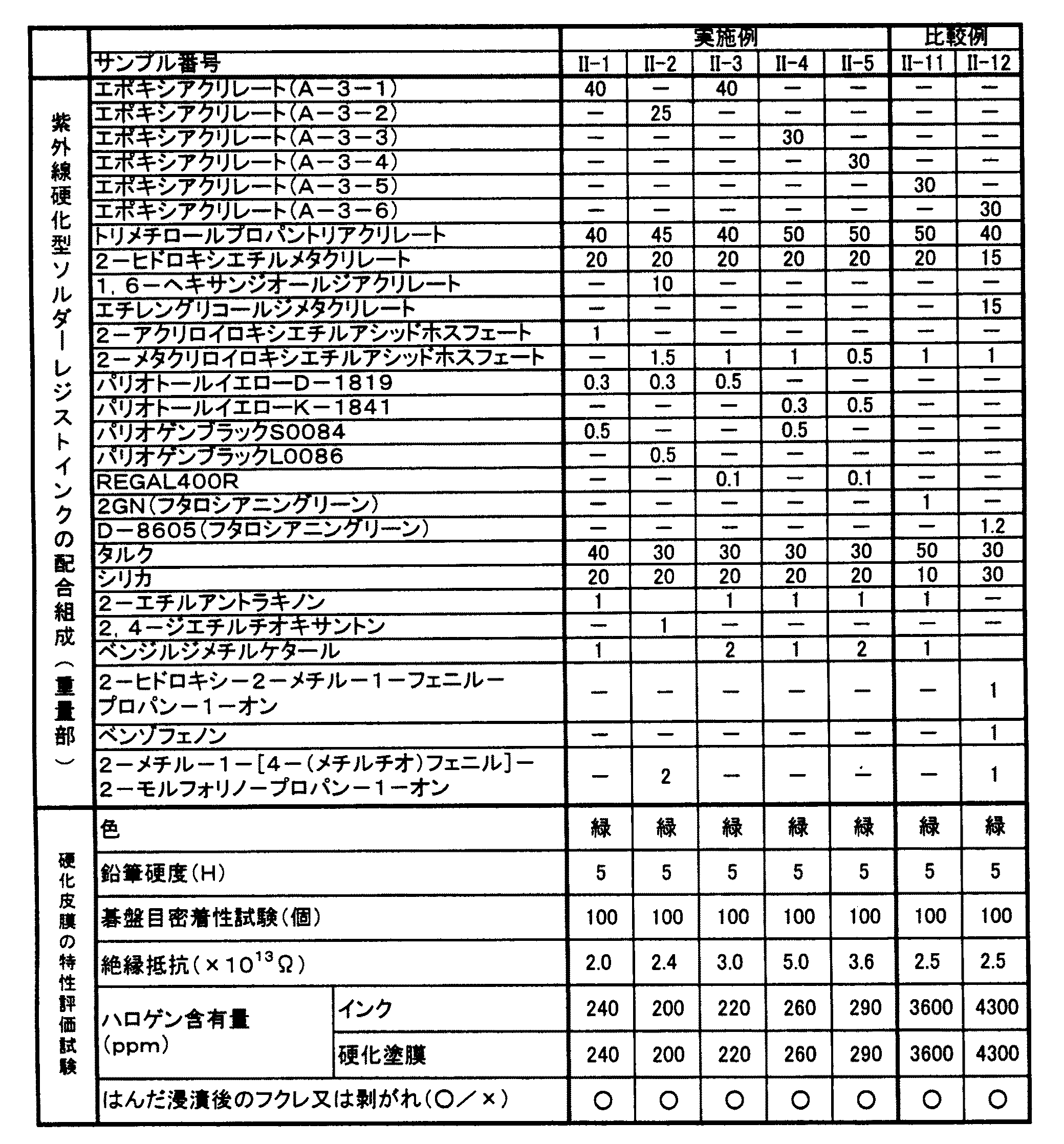
【表2】
本発明のフォトソルダーレジストインクおよび紫外線硬化型ソルダーレジストから形成された塗膜は、表1に記載の結果より、本発明の範囲から外れる従来のフォトソルダーレジストインクおよび紫外線硬化型ソルダーレジストから形成された塗膜と略同等の硬度、耐剥離性、耐熱性および絶縁性を有していた。
さらに、本発明のフォトフォトソルダーレジストインクおよび紫外線硬化型ソルダーレジストから形成された塗膜は、従来のインクから形成されたと膜に比べて、ハロゲン含有量が極めて低くなっている。従って、この塗膜の燃焼時におけるハロゲンガス発生量は、従来よりも、著しく低くなるものと考えられる。
また、本発明において使用した着色顔料は、分散性が良好であるため各成分を配合して混合することにより容易に調製することができた。[0001]
BACKGROUND OF THE INVENTION
The present invention relates to a solder resist ink for forming a permanent protective film of a printed wiring board. More specifically, the present invention By irradiation The present invention relates to a cured solder resist ink.
In particular, the present invention relates to a photo solder resist ink that can be developed with a dilute alkaline aqueous solution, and a non-developing type ultraviolet curable solder resist. In this solder resist, the amount of toxic gas generated during combustion is significantly reduced.
[0002]
[Prior art]
A printed wiring board used in an electric product has a predetermined wiring formed on a substrate such as a copper clad laminate. This printed wiring board prevents the adhesion of solder to unnecessary parts during soldering, avoids electrical shorts, etc. and forms conductor wiring on the board to prevent shortening its life Thereafter, a permanent protective film made of a cured product of solder resist ink is generally formed in a predetermined pattern.
Conventionally, substrates and solder resist inks constituting such printed wiring boards contain halides such as bromide, and toxic gases may be generated during combustion, which has been a problem.
[0003]
However, development of a printed wiring board that does not generate toxic gas at the time of combustion has been demanded due to the recent increase in concern about environmental problems and safety for human bodies. In response to such a demand, for example, a substrate such as a dehalogenated glass epoxy copper-clad laminate has been developed, but with regard to the solder resist ink, a sufficient reduction in halogen content has been achieved. Not in.
[0004]
In general, the permanent protective film of the solder resist ink formed on the printed wiring board is required to be excellent in visibility during visual inspection and gentle to the eyes. For this reason, the permanent protective film exhibits a green color. It is required that
Therefore, the conventional solder resist ink is blended with a coloring pigment such as phthalocyanine green and exhibits a green color. However, this phthalocyanine green contains a high proportion of chlorine and bromine in its chemical structural formula.
Specifically, for example, phthalocyanine green whose color index is Pigment Green 7 contains about 47% by weight of chlorine in one molecule, and phthalocyanine green which is Pigment Green 36 is about 5% by weight in one molecule. And about 60% by weight bromine.
Therefore, a conventional solder resist ink formed by blending a color pigment containing a high proportion of halogen such as phthalocyanine green generates a large amount of toxic gas when burned.
[0005]
[Problems to be solved by the invention]
Therefore, an object of the present invention is to provide a solder resist ink that does not contain halogen or has a significantly reduced halogen content.
[0006]
[Means for Solving the Problems]
The first invention of the present application is
(A) UV curable component,
(B) a photopolymerization initiator, and
(C) A solder resist ink comprising a colored pigment composed of a yellow pigment containing no halogen in the chemical structural formula and a black pigment containing no halogen in the chemical structural formula so as to exhibit a green color. is there.
[0007]
The second invention of the present application is
(A-1) an ultraviolet curable resin having an ethylenically unsaturated group and a carboxyl group in the side chain;
(B) a photopolymerization initiator, and
(C) A solder resist ink comprising a colored pigment composed of a yellow pigment containing no halogen in the chemical structural formula and a black pigment containing no halogen in the chemical structural formula so as to exhibit a green color. is there. This solder resist ink has a particular use as a photo solder resist ink.
[0008]
Furthermore, it is preferable that (A-4) an ethylenically unsaturated monomer is included as an ultraviolet curable component of the photo solder resist ink.
The solder resist ink preferably further contains (D) an organic solvent.
The solder resist ink of the second invention of the present application preferably further comprises (E) a polyfunctional epoxy compound.
The halogen content in the cured product of the solder resist ink is preferably 500 ppm or less.
In addition, the ultraviolet curable resin as the component (A-1) and the polyfunctional epoxy compound as the component (E) blended in the solder resist kink are, for example, epoxy containing no halogen synthesized by a peracid method. When using the compound (A-1) and / or the component (E) prepared from the compound or the epoxy compound that has been subjected to the treatment for reducing the halogen content, The halogen content in the cured product of the photo solder resist ink of the present invention can be reduced to 150 ppm or less.
Moreover, it is preferable that the coloring pigment as the (C) component is the yellow pigment and the said black pigment mix | blended by weight ratio 1: 10-10: 1.
[0009]
The third invention of the present application is
(A-3) an esterified product of an epoxy (meth) acrylate and / or a polyhydric phenol polyether and (meth) acrylic acid,
(A-4) an ethylenically unsaturated compound other than the component (A-3),
(B) a photopolymerization initiator, and
(C) A solder resist ink comprising a colored pigment composed of a yellow pigment containing no halogen in the chemical structural formula and a black pigment containing no halogen in the chemical structural formula so as to exhibit a green color. is there. This solder resist ink is particularly used as an ultraviolet curable solder resist ink.
[0010]
The halogen content in the cured product of the ultraviolet curable solder resist ink of the third invention of the present application is preferably 500 ppm or less.
Further, the color pigment is preferably a combination of a weight ratio of 1:10 to 10: 1 of a yellow color pigment not containing halogen in the chemical structural formula and a black color pigment not containing halogen in the chemical structural formula.
The present invention is described in further detail below.
[0011]
DETAILED DESCRIPTION OF THE INVENTION
The solder resist ink of the present invention comprises (A) an ultraviolet curable component, (B) a photopolymerization initiator, and (C) a yellow pigment that does not contain halogen in the chemical structural formula and a black that does not contain halogen in the chemical structural formula. Contains pigments.
[0012]
(A) UV curable component
In the solder resist ink of the present invention, an ultraviolet curable component is blended as the component (A). This ultraviolet curable component is a component having an ultraviolet curable function, and the solder resist ink of the present invention containing this ultraviolet curable component together with a photopolymerization initiator as the component (C) described below is cured when irradiated with ultraviolet rays. To do.
[0013]
In addition, when the below-mentioned (D) organic solvent is contained, (A) UV curable component in all the components of the solder resist ink of the present invention excluding the organic solvent is preferably contained in an amount of 20 to 80% by weight. Yes.
[0014]
The (A) ultraviolet curable component to be blended in the present invention is not particularly limited as long as it is cured by ultraviolet irradiation. For example, an ultraviolet curable resin having a photoreactive double bond or a photopolymerizable single component. It is arbitrarily selected from conventionally known UV curable components such as a monomer.
[0015]
(B) Photopolymerization initiator
The solder resist ink of the present invention contains a photopolymerization initiator as the component (B) in addition to the above (A) ultraviolet curable component.
The above-mentioned photopolymerization initiator included in the present invention is not particularly limited. Examples of suitable photopolymerization initiators for the present invention include benzoin; benzoin alkyl such as benzoin methyl ether, benzoin ethyl ether, and benzoin isopropyl ether. Ethers; acetophenones such as acetophenone, 2,2-dimethoxy-2-phenylacetophenone, 2,2-diethoxy-2-phenylacetophenone, and 1-hydroxycyclohexyl phenyl ketone; 2-methylanthraquinone, 2-ethylanthraquinone and 2 Anthraquinones such as amylanthraquinone; thioxanthones such as 2,4-dimethylthioxanthone, 2,4-diethylthioxanthone, and 2,4-diisopropylthioxanthone; acetophenone dimethyl Ketals such as luketal and benzyldimethyl ketal; benzophenone, 3,3-dimethyl-4-methoxybenzophenone, 3,3 ′, 4,4′-tetra- (t-butylperoxylcarbonyl) benzophenone and 4-benzoyl-4 Benzophenones or xanthones such as methyldiphenyl sulfide; α-hydroxyketones such as 2-hydroxy-2-methyl-1-phenyl-propan-1-one and 1-hydroxy-cyclohexyl-phenyl-ketone; -1- [4- (Methylthio) phenyl] -2-morpholino-propan-1-one, 2-benzoyl-2-dimethylamino-1- (4-morpholinophenyl) -butanone-1,4,4′- Containing nitrogen atoms such as bis-diethylaminobenzophenone; 2 4,6-trimethyl benzoyl diphenyl phosphine oxide, and the like.
These (B) photopolymerization initiators are blended alone or in appropriate combination in order to prepare the solder resist ink of the present invention.
In addition, these photopolymerization initiators are known light such as tertiary amines such as benzoic acid, p-dimethylaminobenzoic acid ethyl ester, p-dimethylaminobenzoic acid isoamyl ester, 2-dimethylaminoethylbenzoate and the like. You may use together with a polymerization accelerator, a sensitizer, etc.
[0016]
The photopolymerization initiator as the component (B) is preferably 0.1 to 30 in the total components of the solder resist ink of the present invention excluding the organic solvent when the organic solvent described later (D) is included. % By weight, further 0.1 to 10% by weight, optimally 0.1 to 7% by weight. When the photopolymerization initiator is included in the blending amount in the above range, the solder resist ink of the present invention exhibits excellent photocurability, and the physical properties of the obtained permanent protective film are also improved.
[0017]
(C) Colored pigment
Further, the solder resist ink of the present invention contains a coloring pigment as the component (C). The colored pigment blended in the present invention is composed of a yellow pigment containing no halogen in the chemical structural formula and a black pigment containing no halogen in the chemical structural formula, and these yellow pigment and black pigment are The obtained solder resist ink of the present invention and the cured film thereof are blended in such a ratio that it substantially exhibits a green color. Here, the ratio that is substantially green means that the hue or hue is sufficient to allow a viewer to recognize that the solder resist ink or its cured film is green when it is observed with the naked eye. A ratio that has Thereby, the pattern of the printed wiring board produced using the solder resist ink of the present invention is excellent in visibility during visual inspection and is easy on the eyes.
[0018]
Examples of yellow pigments that do not contain halogen in the chemical structural formula constituting the component (C) include C.I. I. Examples include those classified as pigment yellow.
In addition, C.I. I. Among pigment yellows, in particular, isoindoline pigments represented by Color Index (CI) Pigment Yellow 139 and 185,
Benzimidazolone pigments represented by Color Index (CI) Pigment Yellow 120, 151, 175, 180, 181 and 194,
A condensed polycyclic pigment represented by Color Index (CI) Pigment Yellow 148, 182 and 192,
Bisazomethine pigments represented by Color Index (CI) Pigment Yellow 101,
Monoazo pigments represented by Color Index (CI) Pigment Yellow 1, 4, 5, 7, 9, 65, 74, 150, 154 and 167,
Anthraquinone pigments represented by Color Index (CI) Pigment Yellow 24, 108, 123, 147 and 193,
Bisazo pigments represented by Color Index (CI) Pigment Yellow 155,
A metal complex pigment represented by Color Index (CI) Pigment Yellow 117, 129, 153, 177 and 179,
Flavantron yellow indicated by color index (CI) pigment yellow 24,
An iron oxide pigment represented by Color Index (CI) Pigment Yellow 42 and the like;
Examples thereof include azo lake pigments represented by Color Index (CI) Pigment Yellow 61, 62, 100, 104, 133, 168 and 169. These suitable yellow pigments are blended alone or in appropriate combination.
[0019]
Examples of the black pigment not containing halogen in the chemical structural formula constituting the component (C) include C.I. I. The thing classified as pigment black is illustrated.
In addition, the color index exemplified above is C.I. I. Among pigment blacks, in particular, carbon black pigments represented by color index (CI) pigment black 6, 7, 9 and 18, etc.
Graphite pigments represented by Color Index (CI) Pigment Black 8 and 10, etc.,
Perylene pigments represented by color index (CI) pigment black 31 and 32,
Iron oxide pigments represented by color index (CI) pigment black 11, 12 and 27,
Cobalt oxide pigments represented by Color Index (CI) Pigment Black 13, 25, 29, etc.
A copper oxide pigment represented by Color Index (CI) Pigment Black 15 and 28,
Manganese pigments represented by color index (CI) pigment black 14 and 26,
An antimony oxide pigment represented by Color Index (CI) Pigment Black 23,
A nickel oxide pigment represented by a color index (CI) pigment black 30;
Examples thereof include pigments represented by a color index (CI) pigment black 34 and the like.
Moreover, molybdenum sulfide, bismuth sulfide, etc. can be illustrated.
These suitable black pigments are used alone or in appropriate combination.
Further, among the preferred black pigments exemplified above, carbon black pigments, graphite pigments, and perylene pigments represented by color index (CI) pigment blacks 31 and 32 are particularly preferable. In particular, this perylene pigment has a reflection region in a region of 400 nm or more, and a photo solder resist ink containing this perylene pigment has excellent photosensitivity.
[0020]
The yellow pigment and the black pigment are preferably combined in a weight ratio of 1:10 to 10: 1, more preferably 1: 5 to 5: 1. More preferably, they are combined at a weight ratio of 10 to 30 parts by weight of the black pigment with respect to 100 parts by weight of the yellow pigment. By combining the yellow pigment and the black pigment in the above range, the obtained solder resist ink or its cured film becomes substantially green. Even if the color of the solder resist ink itself of the present invention is not necessarily green, the cured product of the solder resist ink of the present invention is only required to be green on the bronze copper-clad laminate.
The colored pigment (C) composed of a yellow pigment and a black pigment blended in the above range has a good dispersibility in other components of the solder resist ink of the present invention and a bright green color with little color unevenness. A solder resist ink that forms a permanent protective film can be obtained.
[0021]
Further, the blending amount of the (C) colored pigment in the solder resist ink of the present invention is not particularly limited. However, this (C) colored pigment, except for (D) an organic solvent, excludes this organic solvent. The solder resist of the present invention preferably contains 0.01 to 20% by weight, more preferably 0.1 to 10% by weight, and most preferably 0.2 to 5% by weight. When the blending amount of the color pigment is in the above range, a permanent protective film having good visibility at the time of visual inspection can be formed while suppressing a decrease in resin curability due to a decrease in ultraviolet transmittance.
[0022]
In addition, the phthalocyanine green pigment used conventionally has a relatively poor dispersibility because the particles are difficult to be miniaturized. Therefore, a long kneading step is required when blending and preparing the solder resist ink so as not to adversely affect the surface state, electrical characteristics, moisture resistance, etc. of the coating film. However, since the above-mentioned colored pigment (C) has good dispersibility in other components as compared with phthalocyanine green and is kneaded and blended relatively easily, the solder resist ink of the present invention can be easily prepared. can do.
[0023]
(I) Photo solder resist ink
When the solder resist ink of the present invention is used as a photo solder resist ink, an ultraviolet curable resin is included so that the ink can be developed with an organic solvent or a dilute alkaline aqueous solution. In particular, when the ink can be developed with a dilute alkaline aqueous solution, the ultraviolet curable component as the component (A) is an ultraviolet ray having an ethylenically unsaturated group and a carboxyl group in the side chain (A-1). A curable resin can be suitably used.
In particular, in the case of the above-described photo solder resist ink, it comprises (A-1) an ultraviolet curable resin having an ethylenically unsaturated group and a carboxyl group in the side chain, (B) a photopolymerization initiator, and (C) a coloring pigment. It is preferable.
[0024]
In the present invention, the “photo solder resist ink” refers to a so-called development-type solder resist ink. For example, the solder resist ink applied on the substrate is selectively exposed to ultraviolet rays to expose the exposed portion. The solder resist ink is cured, and then the unexposed part of the solder resist ink is cured. For example This corresponds to the type of solder resist ink that is washed and removed in a dilute alkaline aqueous solution to obtain a permanent protective film having a predetermined pattern.
[0025]
(A-1) UV curable resin having an ethylenically unsaturated group and a carboxyl group in the side chain
In the photo solder resist ink of the present invention, an ultraviolet curable resin having an ethylenically unsaturated group and a carboxyl group in the side chain is blended as the component (A-1). Since this (A-1) component has a photocurable ethylenically unsaturated group and a carboxyl group in its chemical structural formula, when a predetermined energy is absorbed by exposure to ultraviolet rays or the like, an exposed portion due to this is absorbed. Is cured and the dispersibility and solubility in a dilute alkaline aqueous solution are reduced. Accordingly, the photo solder resist ink of the present invention containing the component (A-1) applied to the substrate is selectively exposed to cure the exposed portion of the photo solder resist ink, and then the substrate is diluted with a dilute alkaline aqueous solution. When the uncured photo-solder resist ink in the unexposed portion is dissolved and removed with a dilute aqueous alkali solution, a predetermined pattern is formed on the substrate.
[0026]
Here, the ultraviolet curable resin of the component (A-1) has a photopolymerizable ethylenically unsaturated group in its chemical structural formula. Examples of such photopolymerizable ethylenically unsaturated groups include unsaturated groups such as (meth) acryloyl groups and vinyl groups. The content of the photopolymerizable ethylenically unsaturated group is not particularly limited, but the content of the unsaturated group in the ultraviolet curable resin is preferably 0.01 to 10 mol / Kg (ultraviolet curable resin), particularly preferably. 0.1 to 5 mol / Kg. When the content of the unsaturated group in the ultraviolet curable resin is in the above range, a photo solder resist ink having particularly excellent exposure sensitivity and developability can be prepared.
[0027]
The ultraviolet curable resin as the component (A-1) preferably has an acid value of 30 to 200 mgKOH / g, particularly 40 to 160 mgKOH / g. When the acid value of the ultraviolet curable resin is in the above range, the compatibility with other components is improved, and a photo solder resist ink having particularly good exposure sensitivity, developability and resolution is prepared. be able to.
[0028]
Further, the weight average molecular weight of the ultraviolet curable resin as the component (A-1) is not particularly limited, but is 3,000 to 400,000, particularly 5,000 to 100,000, and optimally 5, It is preferable that it is 000-50,000. When the weight average molecular weight of the ultraviolet curable resin is in the above range, the balance of resolution and exposure sensitivity of the photo solder resist ink of the present invention is particularly excellent.
[0029]
Examples of the component (A-1) include, for example, an “ethylenically unsaturated compound having a carboxyl group” and a “polyvalent carboxylic acid anhydride” in the epoxy group in the “polymer having an epoxy group in a side chain”. An ultraviolet curable resin formed by addition is exemplified.
[0030]
As the “polymer having an epoxy group in the side chain (skeleton polymer)” for preparing the ultraviolet curable resin exemplified as the component (A-1), the following epoxy compound and ethylenically unsaturated monomer And a copolymer with the body.
That is, examples of the epoxy compound include glycidyl (meth) acrylates such as glycidyl (meth) acrylate and 2-methylglycidyl (meth) acrylate, and (meth) acrylates such as (3,4-epoxycyclohexyl) methyl (meth) acrylate. ) Epoxycyclohexyl derivatives of acrylic acid and the like.
Examples of the ethylenically unsaturated monomer include aliphatic or alicyclic alkyl (meth) acrylates; aromatic (meth) acrylates such as benzyl (meth) acrylate; hydroxyethyl (meth) acrylate and methoxy Ethylene glycol ester (meth) acrylate such as ethyl (meth) acrylate, polyethylene glycol ester (meth) acrylate and propylene glycol (meth) acrylate; (meth) acrylamide compound; N-substituted maleimide compound; vinyl pyrrolidone; (Meth) acrylonitrile; vinyl acetate; styrene; α-methylstyrene; and vinyl ether.
In this specification, (meth) acrylic acid is a generic term for acrylic acid and methacrylic acid, and (meth) acrylate is a generic term for acrylate and methacrylate.
[0031]
In addition, as the “polymer having an epoxy group in the side chain (skeleton polymer)” for preparing the ultraviolet curable resin exemplified as the component (A-1), the epoxy compound and the ethylenically unsaturated monomer In addition to the copolymer, for example, phenol novolac type epoxy resin, cresol novolac type epoxy resin, bisphenol A type epoxy resin, bisphenol F type epoxy resin, bisphenol A-novolak type epoxy resin, alicyclic epoxy resin (for example, "EHPE-3150" manufactured by Daicel Chemical Industries, Ltd.) and polyfunctional epoxy resins that are derivatives of tris (hydroxyphenyl) methane (for example, EPPN-502H manufactured by Nippon Kayaku Co., Ltd., and Tactex-742 manufactured by Dow Chemical Co., Ltd.) And epoxy resins such as XD-9053) Can.
[0032]
Examples of the “ethylenically unsaturated monomer having a carboxyl group” for preparing the ultraviolet curable resin exemplified as the component (A-1) include (meth) acrylic acid, crotonic acid, and cinnamic acid. 2- (meth) acryloyloxyethyl succinic acid, 2- (meth) acryloyloxyethyl phthalic acid, β-carboxyethyl acrylate, acryloyloxyethyl succinate, 2-propenoic acid, 3- (2-carboxyethoxy) Those having one ethylenically unsaturated group such as -3-oxypropyl ester, 2- (meth) acryloyloxyethyltetrahydrophthalic acid and 2- (meth) acryloyloxyethylhexahydrophthalic acid, and pentaerythritol tri (meta ) Acrylate, trimethylolpropane di (me ) Acrylates, those having a plurality of ethylenically unsaturated groups such as those obtained by reacting a dibasic acid anhydride to a polyfunctional acrylate having a hydroxyl group such as dipentaerythritol penta (meth) acrylate.
Among these, those having one carboxyl group are preferable, and it is particularly preferable to use (meth) acrylic acid or (meth) acrylic acid as a main component. This is because the ethylenically unsaturated group introduced by (meth) acrylic acid is excellent in photoreactivity.
These “ethylenically unsaturated monomers having a carboxyl group” can be used alone or in appropriate combination.
[0033]
Examples of the “polycarboxylic anhydride” for preparing the ultraviolet curable resin exemplified as the component (A-1) include succinic anhydride, methyl succinic anhydride, maleic anhydride, and citraconic anhydride. Dibasic acid anhydrides such as glutaric anhydride, itaconic anhydride, phthalic anhydride, tetrahydrophthalic anhydride, methyltetrahydrophthalic anhydride, methyl nadic anhydride, hexahydrophthalic anhydride and methylhexahydrophthalic anhydride, and anhydrous Examples include acid anhydrides of three or more basic acids such as trimellitic acid, pyromellitic anhydride, benzophenone tetracarboxylic anhydride, and methylcyclohexene tetracarboxylic anhydride.
Each of these “polycarboxylic anhydrides” can be used alone or in appropriate combination.
[0034]
Examples of the component (A-1) include addition of an ethylenically unsaturated compound having a carboxyl group and a polyvalent carboxylic acid anhydride to the epoxy group of the polymer having an epoxy group in the side chain as described above. The addition reaction for preparing the ultraviolet curable resin is performed, for example, by heating to about 60 to 150 ° C. in the presence of a thermal polymerization inhibitor and an addition catalyst.
In the above addition reaction, “polycarboxylic acid anhydride” may be added after adding “ethylenically unsaturated compound having carboxyl group” to “polymer having epoxy group in side chain”, In addition, “polycarboxylic acid anhydride” may be added to “polymer having an epoxy group in a side chain” and then “ethylenically unsaturated compound having a carboxyl group” may be added, but the former is preferable. .
[0035]
The photo solder resist ink of the present invention excluding the organic solvent described later In all ingredients The blending amount of the component (A-1) is not particularly limited, but is preferably 10 to 80% by weight, more preferably 20 to 70% by weight, and most preferably 25 to 60% by weight. When the blending amount of the component (A-1) is in the above range, a photo solder resist ink having good alkali developability, sensitivity, and resolution can be obtained.
[0036]
(A-4) Ethylenically unsaturated monomer
In addition to the above (A-1), the photo solder resist ink of the present invention is further coated with (A) an ethylenically unsaturated monomer (A-4) as an ultraviolet curable component. Properties such as heat resistance, heat resistance, and insulation may be improved. The (A-4) photopolymerizable ethylenically unsaturated monomer serves as a diluent and also serves to adjust exposure sensitivity.
Examples of such ethylenically unsaturated monomers include 2-hydroxyethyl (meth) acrylate, 2-hydroxypropyl (meth) acrylate, N-vinylpyrrolidone, (meth) acryloylmorpholine, methoxytetraethylene glycol (meth). Acrylate, methoxy polyethylene glycol (meth) acrylate, polyethylene glycol di (meth) acrylate, N, N-dimethyl (meth) acrylamide, N-methylol (meth) acrylamide, N, N-dimethylaminopropyl (meth) acrylamide, N, N-dimethylaminoethyl (meth) acrylate, melamine (meth) acrylate, diethylene glycol di (meth) acrylate, triethylene glycol di (meth) acrylate, propylene glycol di (meth) Acrylate, phenoxyethyl (meth) acrylate, tetrahydrofurfuryl (meth) acrylate, cyclohexyl (meth) acrylate, trimethylolpropane di (meth) acrylate, trimethylolpropane tri (meth) acrylate, pentaerythritol tri (meth) acrylate, penta Erythritol tetra (meth) acrylate, dipentaerythritol penta (meth) acrylate, dipentaerythritol hexa (meth) acrylate, isobornyl (meth) acrylate, cyclopentanyl mono (meth) acrylate and cyclopentenyl mono (meth) acrylate; polybasic Monoester, diester, triester or polyester of acid and hydroxyalkyl (meth) acrylate; polyester (me ) Acrylate, urethane (meth) (meth) acrylate monomers such as acrylate.
These ethylenically unsaturated monomers are blended singly or in appropriate combination in order to prepare the photo solder resist ink of the present invention.
[0037]
The blending amount of the (A-4) ethylenically unsaturated monomer in all components of the photo solder resist ink excluding the organic solvent is not particularly limited, but is preferably 1 to 50% by weight, and more preferably 1 to 40% by weight. %, Optimally 1-30% by weight. By blending a photopolymerizable ethylenically unsaturated monomer in the above range, the dry coating film has an appropriate surface tackiness, and a negative mask for exposure by applying a negative mask depicting a pattern to the dry coating film Can prevent the problem of fouling.
[0038]
In addition, the photo solder resist ink of the present invention may further include an ethylenic resin such as an ultraviolet curable polymer such as epoxy (meth) acrylate, a (meth) acrylic acid ester copolymer, and a styrene-maleic acid resin, if necessary. You may mix | blend the polymer of an unsaturated compound, or the ultraviolet curable polymer which introduce | transduces an ethylenically unsaturated group further into these.
[0039]
(B) Photopolymerization initiator
The photo solder resist ink of the present invention further contains a photopolymerization initiator as component (B).
[0040]
As the component (B), the photopolymerization initiators listed above are preferably used.
[0041]
Further, the photopolymerization initiator as the component (B) in all the components of the photo solder resist ink of the present invention excluding the organic solvent is preferably 0.1 to 30% by weight, more preferably 1 to 10% by weight, optimally. 1 to 7% by weight. When the photopolymerization initiator is contained in the blending amount in the above range, the photo solder resist ink of the present invention exhibits excellent photocurability and the physical properties of the obtained permanent protective film are also improved.
[0042]
(C) Colored pigment
Further, the photo solder resist ink of the present invention contains a color pigment as the component (C). As described above, the colored pigment blended in the present invention is composed of a yellow pigment that does not contain halogen in the chemical structural formula and a black pigment that does not contain halogen in the chemical structural formula. The yellow pigment and the black pigment are blended in such a ratio that the resulting photo solder resist ink of the present invention and its cured film are substantially green. Thereby, the pattern of the printed wiring board produced using the photo solder resist ink of the present invention is excellent in visibility during visual inspection and is easy on the eyes.
[0043]
Suitable yellow pigments and black pigments are the same as those listed above.
[0044]
Here, the weight ratio of the yellow pigment to the black pigment is also preferably 1:10 to 10: 1, and more preferably 1: 5 to 5: 1, as described above. More preferably, they are combined at a weight ratio of 10 to 30 parts by weight of the black pigment with respect to 100 parts by weight of the yellow pigment. By blending a yellow pigment and a black pigment in the above range, the resulting photo solder resist ink or its cured film is substantially green.
In addition, the yellow pigment and black pigment blended in the above range form a vivid green permanent protective film with good dispersibility in each component of the photo solder resist ink of the present invention and little color unevenness. A photo solder resist ink can be obtained.
[0045]
Further, the blending amount of the (C) coloring pigment is not particularly limited, but the (C) coloring pigment is preferably 0.1 to 0.1 in all components of the photo solder resist ink of the present invention excluding the organic solvent described later. It is contained in an amount of 20% by weight, further 0.1 to 10% by weight, and optimally 0.2 to 1.5% by weight. When the blending amount of the color pigment is in the above range, a permanent protective film having good visibility at the time of visual inspection can be formed while suppressing a decrease in resin curability due to a decrease in ultraviolet transmittance.
[0046]
(D) Organic solvent
The photo solder resist ink of the present invention may further contain an organic solvent as component (D).
As the organic solvent suitable for the present invention, for example, primary having a linear or branched carbon chain such as ethanol, propyl alcohol, isopropyl alcohol, butyl alcohol, isobutyl alcohol, 2-butyl alcohol, hexanol and ethylene glycol, Secondary or polyhydric alcohols; Ketones such as methyl ethyl ketone and cyclohexanone; Aromatic hydrocarbons such as toluene and xylene; Swazol series (manufactured by Maruzen Petrochemicals) and Solvesso series (manufactured by Exxon Chemical) Petroleum-based aromatic mixed solvents of the following: cellosolves such as cellosolve and butylcellosolve; carbitols such as carbitol and butylcarbitol; propylene glycol alkyl ethers such as propylene glycol methyl ether Polypropylene glycol alkyl ethers such as dipropylene glycol methyl ether; Acetic esters such as ethyl acetate, butyl acetate, cellosolve acetate, butyl cellosolve acetate, butyl carbitol acetate and propylene glycol monomethyl ether acetate; and dialkyl glycol ethers . These organic solvents are blended singly or in appropriate combination in order to prepare the photo solder resist ink of the present invention.
[0047]
The organic solvent as the component (D) is preferably 1 to 95% by weight, more preferably 5 to 95% by weight, and most preferably 20 to 95% by weight in the photo solder resist ink of the present invention. . By blending the organic solvent in the above range, the obtained photo solder resist ink of the present invention is excellent in coating properties on the substrate.
[0048]
(E) Polyfunctional epoxy compound
In the photo solder resist ink of the present invention, in addition to the (A-1) ultraviolet curable resin, an (E) polyfunctional epoxy compound as an optional component may be blended.
Although it does not specifically limit as said polyfunctional epoxy compound, For example, bisphenol A type epoxy resin, bisphenol F type epoxy resin, phenol novolak type epoxy resin, cresol novolak type epoxy resin, bisphenol A-novolak type epoxy resin, N-glycidyl Type epoxy resin or cycloaliphatic epoxy resin (for example, “EHPE-3150” manufactured by Daicel Chemical Industries, Ltd.), “YX-4000” (epoxy resin manufactured by Yuka Shell Epoxy Co., Ltd.), hydrogenated bisphenol A type epoxy resin and triglycidyl isocyanurate And polyfunctional epoxy resins derived from tris (hydroxyphenyl) methane (EPPN-502H manufactured by Nippon Kayaku Co., Ltd., Tactex-742 and XD-9053 manufactured by Dow Chemical Co., Ltd.), and the like. In addition, a homopolymer or copolymer of an ethylenically unsaturated monomer having an epoxy group may be used as the polyfunctional epoxy compound of the present invention. In addition, when the copolymer of the left is used, it is preferable that 40 mol% or more of ethylenically unsaturated monomers which have an epoxy group are contained in the monomer which comprises a copolymer. Thereby, good thermosetting can be obtained.
[0049]
Although not particularly limited, when the polyfunctional epoxy compound is a homopolymer or copolymer of an ethylenically unsaturated monomer having an epoxy group, its weight average molecular weight is 2,000 to Preferably it is 200,000. This makes it possible to prepare a photo solder resist ink that forms a cured film having excellent thermosetting properties.
[0050]
The polyfunctional epoxy compound as the component (E) is preferably 0.1 to 50% by weight, more preferably 0.1 to 40% in all components of the photo solder resist ink of the present invention excluding the organic solvent described later. % By weight, optimally 5 to 40% by weight. When the blending amount of the polyfunctional epoxy compound is in the above range, a photo solder resist ink having a good balance between developability and thermosetting property can be obtained.
[0051]
Additional optional ingredients
The photo solder resist ink of the present invention may further contain further optional components in order to improve properties such as coating properties, heat resistance and insulation properties.
Examples of such optional components include extender pigments such as talc, silica, barium sulfate, alumina, calcium carbonate and mica, inorganic pigments, adhesion imparting agents, leveling agents, silane coupling agents, thixotropic agents, and polymerization inhibitors. , Antihalation agents, antifoaming agents, antioxidants, surfactants and polymer dispersants.
[0052]
The photo solder resist ink of the present invention is prepared by a known kneading technique using a three roll, ball mill, sand mill or the like.
In the photo solder resist ink of the present invention, each component is completely and uniformly mixed in advance. No need . For example, for example, the liquid mixture 1 composed of the (E) component and the (D) component and the liquid mixture 2 composed of the (A-1) component, the (B) component, the (C) component, and the (D) component are prepared separately. In addition, the liquid mixture 1 and the liquid mixture 2 may be mixed and used immediately before use.
[0053]
The photo solder resist ink of the present invention is applied onto a substrate such as a copper clad laminate and dried, and a predetermined portion on the obtained dried coating film is irradiated with ultraviolet rays to cure this portion of the photo solder resist ink. To do. Thereafter, the photo-solder resist ink which has been developed by removing the non-exposed portion in a dilute alkaline solution and not removed by the subsequent post-baking becomes a permanent protective film.
The dilute alkali solution used as the developer is preferably an aqueous solution, but may be an aqueous solution containing a hydrophilic organic solvent such as alcohol.
[0054]
The permanent protective film obtained as described above has a halogen content of preferably 500 ppm or less (practically 0.1 to 500 ppm), more preferably 300 ppm or less (practically 0.1 to 300 ppm), optimal. Is 150 ppm or less (practically 0.1 to 150 ppm). This significantly reduces the generation of toxic halogen gases during combustion.
[0055]
According to the present invention, by using a color pigment that does not contain a halogen, the “polymer having an epoxy group in the side chain” in the component (A-1) and the ethylenically unsaturated monomer having an epoxy group used for the production thereof Body, and (E) the polyfunctional epoxy compound and the ethylenically unsaturated monomer having an epoxy group used in the production thereof are not particularly limited. The halogen content can be reduced to 500 ppm or less (practically 0.1 to 500 ppm) as described above.
[0056]
Conventionally, as the above-mentioned epoxy compound for preparing a photo solder resist ink, in particular, an ethylenically unsaturated monomer having a glycidyl group such as an epoxy resin derived from a polycyclic phenol-based compound or glycidyl methacrylate. However, these are industrially produced by addition of epichlorohydrin and elimination of HCl, and the product contains a high concentration of halogen as a reaction by-product or impurity. It was.
For this reason, it has been difficult for the photo solder resist ink prepared using the epoxy compound thus manufactured to have a halogen content in the cured film formed on the substrate of 150 ppm or less.
[0057]
On the other hand, according to the present invention, the epoxy compound used for the production of the component (A-1) and the epoxy compound used for the production of the component (E) or the component (E) are those having a halogen content of 50 ppm or less. It is preferable to do. When such component (A-1) and / or component (E) is used, the halogen content in the permanent protective film formed from the photo solder resist ink of the present invention is significantly reduced as compared with the conventional case. Thus, it can be made 150 ppm or less.
As an epoxy compound having a halogen content of 50 ppm or less as described above for preparing the photo solder resist ink of the present invention, for example, an epoxidation reaction with peracid (for example, formic acid, peracetic acid, perbenzoic acid, etc.) Mention may be made of synthesized epoxy resins and ethylenically unsaturated monomers containing epoxy groups.
These are halogen-free because no epichlorohydrin is used in the production process. Examples of such an epoxy resin include “EHPE-3150” (manufactured by Daicel Chemical Industries, Ltd., an alicyclic epoxy resin), and examples of the ethylenically unsaturated monomer containing an epoxy group include cyclohexane. Mer A-200 (produced by Daicel Chemical Industries, Ltd., ethylenically unsaturated monomer containing an alicyclic epoxy group), cyclomers M-100, M-101 (produced by Daicel Chemical Industries, Ltd., alicyclic) And ethylenically unsaturated monomers containing an epoxy group of the formula).
[0058]
Also, although not synthesized by an epoxidation reaction with a peracid, for example, as an ethylenically unsaturated monomer containing an epoxy group subjected to chlorine reduction treatment, Bremer GS (manufactured by NOF Corporation, chlorine-free, glycidyl) Also in the case of (methacrylate) and the like, the halogen concentration is 10 ppm or less and is preferably used.
[0059]
(II) UV curable solder resist ink
On the other hand, when the solder resist ink of the present invention is used as an ultraviolet curable solder resist ink, the ultraviolet curable component as the component (A) is not particularly limited, but (A-3) epoxy (meta) It is preferably composed of an esterified product of acrylate and / or polyphenolic polyether and (meth) acrylic acid, and (A-4) an ethylenically unsaturated compound other than the component A-3. That is, this ultraviolet curable solder resist ink has (A-3) an epoxy (meth) acrylate and / or an esterified product of a polyhydric phenol polyether and (meth) acrylic acid, other than the component (A-3). (A-4) An ethylenically unsaturated compound, (B) a photopolymerization initiator, and (C) a coloring pigment.
[0060]
In the present invention, the “ultraviolet curable solder resist ink” refers to one that can form a desired pattern by a printing method to form a permanent protective film. For example, a conventionally known method such as screen printing on a substrate is known. This corresponds to a solder resist ink of a type that obtains a permanent protective film having a predetermined pattern by completely exposing the exposed portion of the ultraviolet light to the solder resist ink printed using a printing technique to cure the exposed portion of the solder resist ink. .
[0061]
(A-3) Esterified product of epoxy (meth) acrylate and / or polyphenolic polyether product and (meth) acrylic acid
The ultraviolet curable solder resist ink of the present invention contains, as the component (A-3), an esterified product of an epoxy (meth) acrylate and / or a polyhydric phenol polyether and (meth) acrylic acid.
[0062]
In the present invention, the epoxy (meth) acrylate as the component (A-3) refers to a fully esterified product or a partially esterified product of an epoxy group that can be produced by an esterification reaction between an epoxy compound and (meth) acrylic acid. .
In the present invention, as the (A-3) epoxy (meth) acrylate, conventionally known ones can be used alone or in appropriate combination.
Specific examples of the epoxy compound that generates the epoxy (meth) acrylate include bisphenol A, bisphenol F, bisphenol A resin, bisphenol F resin, cresol novolac resin, and phenol novolac resin. Obtained by reacting polyphenols such as polychlorohydrin and epichlorohydrin, and alicyclic epoxy resins (for example, a peracetic acid-based epoxy resin “EHPE-3150” substantially free of halogens manufactured by Daicel Chemical Industries, Ltd.) Etc.
[0063]
On the other hand, an esterified product of a polyhydric phenol polyether and (meth) acrylic acid as the component (A-3) is produced by an esterification reaction of a polyhydric phenol polyether and (meth) acrylic acid. A fully or partially esterified product that can be produced.
The polyhydric phenol polyether product is obtained, for example, by adding ethylene oxide, propylene oxide, butylene oxide, ε-caprolactone, or the like to the polyhydric phenol.
[0064]
The blending amount of the component (A-3) in the ultraviolet curable solder resist ink of the present invention is not particularly limited, but preferably the component (A-3) is 10 in the ultraviolet curable solder resist ink of the present invention. -70% by weight, further 15-65% by weight, optimally 15-60% by weight. The ultraviolet curable solder resist ink of the present invention containing the component (A-3) in the above range can be cured by irradiation with ultraviolet rays to obtain a cured product having a desired strength.
[0065]
(A-4) Ethylenically unsaturated compounds other than A-3 component
In addition, the ultraviolet curable solder resist ink of the present invention contains an ethylenically unsaturated compound other than the component (A-3) as the component (A-4) in addition to the component (A-3). ing.
Examples of the ethylenically unsaturated compound other than the component (A-3) include those exemplified in the description regarding the photo solder resist described above.
[0066]
The blending amount of the component (A-4) in the ultraviolet curable solder resist ink of the present invention is not particularly limited, but the component (A-4) is preferably 10 to 70% by weight in the ink of the present invention. Is 15 to 65% by weight, optimally 20 to 60% by weight. The ultraviolet curable solder resist ink of the present invention containing the component (A-4) in the above range can be cured by irradiation with ultraviolet rays to obtain a cured product having a desired strength.
[0067]
In addition, the composition ratio of said (A-3) component and (A-4) component which comprises an ultraviolet curable component is not specifically limited. However, the blending ratio of the component (A-3) in the total 100 parts by weight of the component (A-3) and the component (A-4) is preferably 10 to 70 parts by weight, more preferably 10 to 60 parts by weight. It is preferable that it is an ultraviolet curable component which is 15-50 weight part. An ultraviolet curable solder resist ink that forms a permanent protective film having excellent printability and excellent curability and heat resistance when component (A) and component (B) are blended in a blending amount in the above range. Can be prepared.
[0068]
(B) Photopolymerization initiator
The solder resist ink of the present invention contains a photopolymerization initiator as the component (B) in addition to the components (A-3) and (A-4).
Suitable photopolymerization initiators included in the present invention are the same as those listed above.
[0069]
Further, the blending amount of the photoinitiator (B) of the present invention is preferably 0.1 to 30% by weight, more preferably 1 to 10% in the ultraviolet curable solder resist ink of the present invention as described above. % By weight, optimally 1-7% by weight. When the photopolymerization initiator is included in the blending amount in the above range, the solder resist ink of the present invention exhibits excellent photocurability, and the physical properties of the obtained permanent protective film are also improved.
[0070]
(C) Colored pigment
Further, the photo solder resist ink of the present invention contains a color pigment as the component (C). As described above, the colored pigment blended in the present invention is composed of a yellow pigment that does not contain halogen in the chemical structural formula and a black pigment that does not contain halogen in the chemical structural formula. The yellow pigment and the black pigment are blended in such a ratio that the resulting photo solder resist ink of the present invention and its cured film are substantially green. Thereby, the pattern of the printed wiring board produced using the photo solder resist ink of the present invention is excellent in visibility during visual inspection and is easy on the eyes.
[0071]
Examples of the yellow pigment and black pigment not containing halogen in the chemical structural formula constituting the component (C) include those listed above.
[0072]
The weight ratio of the yellow pigment to the black pigment is preferably 1:10 to 10: 1, more preferably 1: 5 to 5: 1, as described above. More preferably, they are combined at a weight ratio of 10 to 30 parts by weight of the black pigment with respect to 100 parts by weight of the yellow pigment. By blending a yellow pigment and a black pigment in the above range, the resulting photo solder resist ink or its cured film is substantially green.
In addition, the yellow pigment and the black pigment blended in the above ranges provide a photo solder resist ink that forms a vivid green permanent protective film with good dispersibility in other components and little color unevenness. be able to.
[0073]
The blending amount of the color pigment as the component (C) in the ultraviolet curable solder resist ink of the present invention is not particularly limited, but the color pigment is 0.01 to 20 in the ultraviolet curable solder resist ink of the present invention. % By weight, further 0.1 to 10% by weight, optimally 0.2 to 5% by weight. The ultraviolet curable solder resist ink of the present invention containing the coloring pigment in the above-mentioned blending amount can form a permanent protective film with good visibility during visual inspection while suppressing a decrease in resin curability due to a decrease in ultraviolet transmittance.
[0074]
The ultraviolet curable solder resist ink of the present invention contains the above components (A-3), (A-4), (B) and (C) as essential components, but printability, heat resistance, insulation, etc. Other components may be included as long as the above properties are not adversely affected.
Examples of such components include extender pigments such as talc, silica, barium sulfate, alumina, calcium carbonate and mica, inorganic pigments, adhesion improvers, leveling agents, thixotropic agents, antifoaming agents and polymerization inhibitors. It is done.
[0075]
The ultraviolet curable solder resist ink of the present invention is printed on a substrate such as a copper clad laminate by adopting a conventionally known printing method such as a screen printing method or an offset printing method.
[0076]
In the ultraviolet curable solder resist ink of the present invention, the halogen content in the ultraviolet curable solder resist ink can be remarkably reduced by using the color pigment (C) containing no halogen. Specifically, the halogen content of the ultraviolet curable solder resist ink of the present invention is 500 ppm or less (practically 0.1 to 500 ppm), preferably 400 ppm or less (practically 0.1 to 400 ppm), Furthermore, it is 300 ppm or less (practically 0.1 to 300 ppm). Therefore, the permanent protective film formed from the ultraviolet curable solder resist ink of the present invention significantly reduces the amount of halogen gas generated during combustion.
On the other hand, when using an epoxy compound for manufacture of (A-3) component, a thing with a halogen content of 50 ppm or less can also be selected as this epoxy compound. As a result, the halogen content in the permanent protective film formed from the solder resist ink of the present invention can be significantly reduced as compared with the conventional case, and can be reduced to 150 ppm or less. This is the same as in the case of resist ink.
[0077]
【Example】
Hereinafter, the present invention will be described in more detail based on examples, but the present invention is not limited to the following examples.
The “parts” and “%” shown below are all based on weight.
[0078]
Example 1
(I) Photo solder resist ink
Samples I-1 to I-6 according to the present invention were prepared with the composition shown in Table 1.
Moreover, in order to compare the performance of the photo solder resist ink of the present invention with the composition shown in Table 1, Samples I-11 to 12 were prepared.
[0079]
In addition, (A-1-1), (A-1-2), (A-1-3), and (A-1-4) used as ultraviolet curable resins described in Table 1 are as follows. It has been prepared.
[Synthesis of A-1-1]
A four-necked flask equipped with a reflux condenser, a thermometer, a glass tube for nitrogen substitution, and a stirrer, 70 parts of Bremer GS (manufactured by NOF, glycidyl methacrylate with reduced chlorine, halogen content of 1 ppm or less), 30 parts of methyl methacrylate Then, 100 parts of carbitol acetate and 3 parts of azobisisobutyronitrile were added, and polymerized by heating at 80 ° C. for 5 hours under a nitrogen stream with stirring to obtain a 50% copolymer solution. To the obtained 50% copolymer solution, 0.05 part of hydroquinone, 37 parts of acrylic acid and 0.2 part of dimethylbenzylamine were added, and an addition reaction was performed at 100 ° C. for 24 hours. Subsequently, 45 parts of tetrahydrophthalic anhydride and 79 parts of carbitol acetate were added and reacted at 100 ° C. for 3 hours to obtain a 50% solution (A-1-1) of an ultraviolet curable resin.
[0080]
[Synthesis of A-1-2]
179 parts of EHPE3150 (alicyclic epoxy resin, manufactured by Daicel Chemical Industries, Ltd., epoxy equivalent 179, containing no halogen (no halogen was detected)) was dissolved in 60 parts of carbitol acetate and further stirred with acrylic. 74 parts of acid, 0.1 part of hydroquinone and 0.7 part of dimethylbenzylamine were added and reacted at 90-100 ° C. for 24 hours by a conventional method. To this reaction liquid, 95 parts of carbitol acetate was added and stirred to obtain an epoxy acrylate solution. Subsequently, 76 parts of tetrahydrophthalic anhydride and 64 parts of carbitol acetate were added and reacted at 100 ° C. for 3 hours to obtain a 60% solution (A-1-2) of an ultraviolet curable resin.
[0081]
[Synthesis of A-1-3]
Instead of the Bremer GS used in the synthesis of (A-1-1) above, Acryester G (produced by Mitsubishi Rayon Co., Ltd., glycidyl methacrylate containing halogen as an impurity obtained by using epichlorohydrin, halogen A 50% solution (A-1-3) of an ultraviolet curable resin was obtained in the same manner as in the synthesis of (A-1-1) except that 70 parts of a content of 1600 ppm was used.
[0082]
[Synthesis of A-1-4]
In place of EHPE3150 used in the synthesis of (A-1-2) above, Epicron N-680 (Cresol novolak type epoxy resin manufactured by Dainippon Ink & Chemicals, Inc., epoxy equivalent 214, halogen content 1050 ppm) was 214. 60% of the ultraviolet curable resin in the same manner as in the synthesis of (A-1-2), except that the amount of carbitol acetate used in combination with the acid anhydride is changed to 78 parts. A solution (A-1-4) was obtained.
[0083]
Moreover, EHPE3150 used as a polyfunctional epoxy compound described in Table 1 is an epoxy resin manufactured by Daicel Chemical Industries, Ltd., and Epicron N-680 is a cresol novolac type epoxy resin manufactured by Dainippon Ink & Chemicals, Inc. Yes, TEPIC-S is triglycidyl isocyanurate (halogen content 800 ppm) manufactured by Nissan Chemical Industries, Ltd.
[0084]
[Synthesis of E-1]
Moreover, (E-1) described in Table 1 was prepared as follows.
That is, in a four-necked flask equipped with a reflux condenser, a thermometer, a glass tube for nitrogen substitution, and a stirrer, 80 parts of Blemmer GS (manufactured by NOF Corporation, chlorine-reduced glycidyl methacrylate), 20 parts of butyl acrylate, Calvi 67 parts of tall acetate and 3 parts of azobisisobutyronitrile were added and polymerized at 85 ° C. for 5 hours under a nitrogen stream with stirring to obtain a 60% solution (E-1) of a polyfunctional epoxy compound.
[0085]
Examples of yellow pigments that do not contain a halogen in the chemical structural formula of the present invention include paliotol yellow D-1819 (Color Index (CI) Pigment Yellow 139) (an isoindoline yellow pigment made by BASF), and paliotol. Yellow K-1841 (color index (CI) pigment yellow 139) (an isoindoline yellow pigment manufactured by BASF) was used.
Examples of black pigments that do not contain a halogen in the chemical structural formula of the present invention include Paliogen Black S0084 (Color Index (CI) Pigment Black 31) (perylene black pigment manufactured by BASF), Paliogen Black L0086 ( Color Index (CI) Pigment Black 32) (perylene-based black pigment manufactured by BASF), and REGAL400R (Color Index (CI) Pigment Black 7) (carbon black manufactured by Cubot Specialty Chemicals Inc.) )It was used.
Conventional green organic pigments include 2GN (Color Index (CI) Pigment Green 7) (phthalocyanine green pigment manufactured by Dainichi Seika Co., Ltd.), and D-8605 (Color Index (CI)). Pigment Green 7) (phthalocyanine green pigment manufactured by BASF) was used.
Irgacure 907 used as a photopolymerization initiator is manufactured by Ciba Geigy, and Kayacure DETX-S is manufactured by Nippon Kayaku Co., Ltd.
Modaflow is a leveling agent manufactured by Monsanto.
Silica having an average particle diameter of 1 μm was used.
[0086]
The photo solder resist inks I-1 to 6 and I-11 to 12 obtained as described above were etched in advance on a copper clad laminate made of a glass epoxy substrate having a copper foil of 35 μm to form a pattern. The whole surface of the printed wiring board was applied by screen printing, and precure was performed at 80 ° C. for 20 minutes in order to volatilize the solvent, thereby obtaining a dry coating film having a thickness of 20 μm. Then, directly apply the mask on which the pattern was drawn to the surface of the coating film, 150 mJ / cm 2 The test piece I-1-6 according to the present invention and the present invention were subjected to heat curing at 150 ° C. for 60 minutes, followed by development with a 1% sodium carbonate aqueous solution as a developer. Test pieces I-11 to 12 out of the range were prepared.
[0087]
Example 2
(II) UV curable solder resist ink
In order to prepare the ultraviolet curable solder resist ink as an example, first, the following epoxy acrylates (A-3-1) to (A-3-6) were prepared.
[0088]
Epoxy acrylate (A-3-1)
This was prepared by esterification reaction from Epicoat 154 (phenol novolac type epoxy resin manufactured by Yuka Shell Epoxy Co., Ltd.) and acrylic acid.
This is a total esterified product of epoxy groups.
[0089]
Epoxy acrylate (A-3-2)
This was prepared by an esterification reaction from Epicoat 828 (bisphenol A type epoxy resin manufactured by Yuka Shell Epoxy Co., Ltd.) and acrylic acid. This is a total esterified product of epoxy groups.
[0090]
Epoxy acrylate (A-3-3)
This was prepared by an esterification reaction from EPPN-201 (a phenol novolac type epoxy resin manufactured by Nippon Kayaku Co., Ltd.) and acrylic acid. This is a total esterified product of epoxy groups.
[0091]
Epoxy acrylate (A-3-4)
This was prepared by an esterification reaction from epiclone N-695 (a cresol novolac type epoxy resin manufactured by Dainippon Ink and Chemicals, Inc.) and acrylic acid. This is a total esterified product of epoxy groups.
[0092]
Epoxy acrylate (A-3-5)
This was prepared by an esterification reaction from Epicoat 152 (phenol novolac type epoxy resin manufactured by Yuka Shell Epoxy Co., Ltd.) and acrylic acid.
This is a total esterified product of epoxy groups.
[0093]
Epoxy acrylate (A-3-6)
This was prepared by esterification reaction from Epicron N-680 (a cresol novolac type epoxy resin manufactured by Dainippon Ink and Chemicals, Inc.) and acrylic acid. This is a total esterified product of epoxy groups.
[0094]
As 2-acryloyloxyethyl acid phosphate, light ester PA manufactured by Kyoeisha Chemical Co., Ltd. was used. In addition, 2-methacryloyloxyethyl acid phosphate used light ester PM manufactured by Kyoeisha Chemical Co., Ltd.
[0095]
Moreover, the same pigment as Example 1 was used for the yellow pigment and black pigment which do not contain a halogen in the chemical structural formula in this invention.
In addition, the conventional green organic coloring pigment used as a comparative example was the same as the pigment used in Example 1.
[0096]
The ultraviolet curable solder resist ink according to the present invention is prepared by uniformly mixing the components prepared as described above at a blending ratio shown in Table 2 and thoroughly kneading them with a three-roll manufactured by Inoue Seisakusho Co., Ltd. II-1 to 5 were obtained.
Moreover, in order to evaluate the performance of the ultraviolet curable solder resist ink of the present invention, the ultraviolet curable solder resist inks II-11 to 12-12, which are out of the scope of the present invention, were similarly prepared.
[0097]
The ultraviolet curable solder resist ink obtained as described above was printed and applied onto a printed wiring board patterned by a screen printing method using a 225 mesh screen. Thereafter, it is cured by irradiating with a light amount of 1000 mJ / cm @ 2 using a 120 W / cm (or 80 W / cm) metal halide lamp (or high-pressure mercury lamp), and test pieces II-1 to 6 according to the present invention and Test pieces II-11 to 12 deviating from the scope of the present invention were obtained.
[0098]
For the test pieces prepared from the (I) photo solder resist ink and (II) UV curable solder resist ink obtained as described above, a pencil hardness test, a cross-cut adhesion test, a solder heat resistance test, A solvent resistance test, a chemical resistance test, an insulation resistance test, and a property evaluation test on the halogen content were performed. The obtained results are also shown in Table 1.
In addition, the method of these characteristic evaluation tests is demonstrated easily below.
[0099]
The pencil hardness test was performed according to JIS K-5400, 8.4. Using a pencil (Mitsubishi Uni), the highest hardness without damage was measured.
[0100]
The cross-cut adhesion test was performed according to JIS K-5400, 8.5. Using an Erichsen crosscut tester, 11 cured films were cut vertically and horizontally and subjected to a cello tape peeling test. The remaining number in 100 grids was counted.
[0101]
The solder heat resistance test was performed according to JIS C-6481, 5.5. LONCO · CF-350 (water-soluble flux manufactured by London Chemical Co., Ltd.) is used as the flux. First, the flux is applied to the test piece, and then immersed in a molten solder bath at 260 ° C. for 10 seconds, and immediately afterwards in cooling water. I put it in. The substrate surface immediately after this test was observed to confirm the presence or absence of swelling or peeling.
[0102]
In the solvent resistance test, the substrate was immersed in 2-propanol and 1,1,1-trichloroethane for 1 hour at room temperature, and the surface of the substrate was observed to confirm the presence or absence of swelling or peeling.
[0103]
In the chemical resistance test, the substrate was immersed in 10 wt% hydrochloric acid and a 10 wt% sodium hydroxide aqueous solution for 1 hour at room temperature, and then the substrate surface was observed to confirm the presence or absence of swelling or peeling.
[0104]
In the insulation resistance test, the resistance between the opposing electrodes of the IPC-B-25 comb pattern having the cured coating film of the present invention was measured.
[0105]
In the case of the photo solder resist ink of Example 1, the halogen content was weighed using the residue obtained by volatilizing and removing the organic solvent from the ink and the cured coating film as samples, and burning these samples. The content of chlorine, bromine and fluorine in the absorbing liquid which burned in the flask and absorbed the generated gas was quantified by ion chromatography analysis measurement.
On the other hand, in the case of the ultraviolet curable solder resist ink of Example 2, the ink and the cured coating film were weighed as samples, and the halogen content was quantified in the same manner as in Example 1 above.
[0106]
[Table 1]
[Table 2]
The coating film formed from the photo solder resist ink and the ultraviolet curable solder resist of the present invention is formed from the conventional photo solder resist ink and the ultraviolet curable solder resist that are out of the scope of the present invention based on the results shown in Table 1. The coating film had almost the same hardness, peel resistance, heat resistance, and insulation properties.
Furthermore, the coating film formed from the photo-photo solder resist ink and the ultraviolet curable solder resist of the present invention has an extremely low halogen content as compared to the film formed from the conventional ink. Therefore, it is considered that the amount of halogen gas generated when the coating film burns is significantly lower than that in the past.
In addition, since the color pigment used in the present invention has good dispersibility, it could be easily prepared by blending and mixing each component.
Claims (13)
(B)光重合開始剤、および
(C)化学構造式中にハロゲンを含まない黄色顔料と化学構造式中にハロゲンを含まない黒色顔料とからなり緑色を呈するように配合された着色顔料を含むことを特徴とするソルダーレジストインク。(A) UV curable component,
(B) a photopolymerization initiator, and (C) a color pigment that is composed of a yellow pigment that does not contain halogen in the chemical structural formula and a black pigment that does not contain halogen in the chemical structural formula so as to exhibit a green color Solder resist ink characterized by that.
(A−1)側鎖にエチレン性不飽和基とカルボキシル基とを有する紫外線硬化性樹脂からなるものであり、
フォトソルダーレジストインクとして利用されることを特徴とする請求項1に記載のソルダーレジストインク。The (A) ultraviolet curable component is composed of an ultraviolet curable resin having an ethylenically unsaturated group and a carboxyl group in the side chain (A-1),
The solder resist ink according to claim 1, wherein the solder resist ink is used as a photo solder resist ink.
(Aー3)エポキシ(メタ)アクリレートおよび/または多価フェノールのポリエーテル化物と(メタ)アクリル酸とのエステル化物、および
前記(Aー3)成分以外の(A−4)エチレン性不飽和化合物からなるものであり、紫外線硬化型ソルダーレジストインクとして利用されることを特徴とする請求項1に記載のソルダーレジストインク。The (A) UV curable component is other than (A-3) an epoxy (meth) acrylate and / or an esterified product of a polyhydric phenol polyether and (meth) acrylic acid, and the component (A-3) (A-4) The solder resist ink according to claim 1, which is made of an ethylenically unsaturated compound and is used as an ultraviolet curable solder resist ink.
Priority Applications (1)
| Application Number | Priority Date | Filing Date | Title |
|---|---|---|---|
| JP2001058254A JP4532002B2 (en) | 2000-03-06 | 2001-03-02 | Solder resist ink |
Applications Claiming Priority (5)
| Application Number | Priority Date | Filing Date | Title |
|---|---|---|---|
| JP2000059913 | 2000-03-06 | ||
| JP2000-59913 | 2000-03-06 | ||
| JP2000-59892 | 2000-03-06 | ||
| JP2000059892 | 2000-03-06 | ||
| JP2001058254A JP4532002B2 (en) | 2000-03-06 | 2001-03-02 | Solder resist ink |
Publications (2)
| Publication Number | Publication Date |
|---|---|
| JP2001324801A JP2001324801A (en) | 2001-11-22 |
| JP4532002B2 true JP4532002B2 (en) | 2010-08-25 |
Family
ID=27342582
Family Applications (1)
| Application Number | Title | Priority Date | Filing Date |
|---|---|---|---|
| JP2001058254A Expired - Fee Related JP4532002B2 (en) | 2000-03-06 | 2001-03-02 | Solder resist ink |
Country Status (1)
| Country | Link |
|---|---|
| JP (1) | JP4532002B2 (en) |
Families Citing this family (15)
| Publication number | Priority date | Publication date | Assignee | Title |
|---|---|---|---|---|
| TWI313282B (en) * | 2005-02-05 | 2009-08-11 | Eternal Chemical Co Ltd | Halogen free dry film photosensitive resin composition |
| CN101921375B (en) * | 2005-04-27 | 2012-12-05 | 三菱化学株式会社 | Curable composition, cured product, and liquid crystal display device using the same |
| JP4793717B2 (en) * | 2005-11-09 | 2011-10-12 | 株式会社タムラ製作所 | Solder resist ink and manufacturing method thereof |
| JP2007217608A (en) * | 2006-02-17 | 2007-08-30 | Sekisui Chem Co Ltd | Ultraviolet curable paste, offset printing apparatus, and method for offset printing |
| JP5352175B2 (en) * | 2008-03-26 | 2013-11-27 | 太陽ホールディングス株式会社 | Photosensitive resin composition, cured product thereof, and printed wiring board having solder resist layer made of the cured product |
| JP5007453B2 (en) * | 2010-06-11 | 2012-08-22 | 株式会社タムラ製作所 | Black curable resin composition |
| US9835942B2 (en) | 2010-12-14 | 2017-12-05 | Kaneka Corporation | Photosensitive resin composition and use thereof |
| US8993897B2 (en) * | 2011-04-25 | 2015-03-31 | Kaneka Corporation | Photosensitive resin composition and use thereof |
| JP5583091B2 (en) * | 2011-08-31 | 2014-09-03 | 株式会社タムラ製作所 | Black curable resin composition |
| WO2013111481A1 (en) | 2012-01-25 | 2013-08-01 | 株式会社カネカ | Novel resin composition for pigment-containing insulating film, and use thereof |
| WO2013171888A1 (en) * | 2012-05-17 | 2013-11-21 | 太陽インキ製造株式会社 | Alkali-development-type thermoset resin composition and printed circuit board |
| JP5695622B2 (en) * | 2012-09-24 | 2015-04-08 | 株式会社タムラ製作所 | Black curable resin composition |
| TW201423272A (en) * | 2012-11-27 | 2014-06-16 | Jsr Corp | Photosensitive composition, colorant dispersion solution, light filter and light sensor |
| JP2015069181A (en) * | 2013-09-30 | 2015-04-13 | Jsr株式会社 | Radiation-sensitive resin composition, cured film, method for forming the same and display element |
| WO2024004421A1 (en) * | 2022-06-30 | 2024-01-04 | Dic株式会社 | Resin composition for powder coating material, powder coating material, and article having coating film of said powder coating material |
Citations (4)
| Publication number | Priority date | Publication date | Assignee | Title |
|---|---|---|---|---|
| JPH07166117A (en) * | 1993-12-16 | 1995-06-27 | Somar Corp | Photo-setting resist ink composition |
| JPH11316457A (en) * | 1998-05-01 | 1999-11-16 | Taiyo Ink Mfg Ltd | Photosensitive resin composition and printed circuit board having solder resist film or resin insulating layer formed from the composition |
| JP2000007974A (en) * | 1998-06-22 | 2000-01-11 | Taiyo Ink Mfg Ltd | Green ink composition for printed wiring board using halogen-free coloring pigment |
| JP2001064534A (en) * | 1999-06-21 | 2001-03-13 | Toyo Ink Mfg Co Ltd | Green pigment composition containing no halogen |
-
2001
- 2001-03-02 JP JP2001058254A patent/JP4532002B2/en not_active Expired - Fee Related
Patent Citations (4)
| Publication number | Priority date | Publication date | Assignee | Title |
|---|---|---|---|---|
| JPH07166117A (en) * | 1993-12-16 | 1995-06-27 | Somar Corp | Photo-setting resist ink composition |
| JPH11316457A (en) * | 1998-05-01 | 1999-11-16 | Taiyo Ink Mfg Ltd | Photosensitive resin composition and printed circuit board having solder resist film or resin insulating layer formed from the composition |
| JP2000007974A (en) * | 1998-06-22 | 2000-01-11 | Taiyo Ink Mfg Ltd | Green ink composition for printed wiring board using halogen-free coloring pigment |
| JP2001064534A (en) * | 1999-06-21 | 2001-03-13 | Toyo Ink Mfg Co Ltd | Green pigment composition containing no halogen |
Also Published As
| Publication number | Publication date |
|---|---|
| JP2001324801A (en) | 2001-11-22 |
Similar Documents
| Publication | Publication Date | Title |
|---|---|---|
| EP1037111B1 (en) | Ultraviolet curable resin composition and photo solder resist ink using the same | |
| JP4203017B2 (en) | Photocurable / thermosetting resin composition and printed wiring board using the same | |
| JP5449688B2 (en) | Photo-curable thermosetting resin composition, dry film and cured product thereof, and printed wiring board using them | |
| JP4532002B2 (en) | Solder resist ink | |
| JP5666868B2 (en) | Resin composition for solder resist and printed wiring board | |
| JP6204734B2 (en) | Resin composition for solder resist | |
| JP4502427B2 (en) | Photo solder resist ink | |
| JP4768924B2 (en) | Photo solder resist ink | |
| WO2010113287A1 (en) | Photosensitive electrically conductive paste and electrode pattern | |
| JPWO2008120491A1 (en) | Photocurable resin composition, dry film, cured product, and printed wiring board | |
| JP4705311B2 (en) | UV curable resin composition and photo solder resist ink containing the composition | |
| JP4847670B2 (en) | UV curable resin composition and photo solder resist ink containing the composition | |
| JP3805745B2 (en) | Solder resist ink | |
| JP3808999B2 (en) | Photoresist ink and printed wiring board manufacturing ink | |
| JP4034555B2 (en) | Photocurable thermosetting conductive composition and method for forming conductive circuit using the same | |
| JP6491417B2 (en) | Resin composition for solder resist, resin composition for marking ink, cured product, and printed wiring board | |
| JPWO2002096969A1 (en) | Photocurable and thermosetting resin composition | |
| JP3808997B2 (en) | Photo-curable printing ink and printed wiring board manufacturing ink | |
| TW517503B (en) | Anti-soldering printing ink | |
| JPWO2004061006A1 (en) | Photocurable thermosetting conductive composition, conductive circuit using the conductive composition, and method for forming the same | |
| JP3808996B2 (en) | Photo-curable printing ink and printed wiring board manufacturing ink | |
| JP2002284842A (en) | Epoxy acrylate compound, curable resin composition containing the same and its cured product | |
| JPH05287036A (en) | Resin composition, solder resist resin composition, and its cured product | |
| JP3180979B2 (en) | Resin composition, solder resist resin composition and cured product thereof | |
| JPH11256088A (en) | Resin composition for alkali-soluble resist ink |
Legal Events
| Date | Code | Title | Description |
|---|---|---|---|
| A621 | Written request for application examination |
Free format text: JAPANESE INTERMEDIATE CODE: A621 Effective date: 20080207 |
|
| RD02 | Notification of acceptance of power of attorney |
Free format text: JAPANESE INTERMEDIATE CODE: A7422 Effective date: 20080207 |
|
| RD04 | Notification of resignation of power of attorney |
Free format text: JAPANESE INTERMEDIATE CODE: A7424 Effective date: 20091007 |
|
| A977 | Report on retrieval |
Free format text: JAPANESE INTERMEDIATE CODE: A971007 Effective date: 20100512 |
|
| TRDD | Decision of grant or rejection written | ||
| A01 | Written decision to grant a patent or to grant a registration (utility model) |
Free format text: JAPANESE INTERMEDIATE CODE: A01 Effective date: 20100519 |
|
| A01 | Written decision to grant a patent or to grant a registration (utility model) |
Free format text: JAPANESE INTERMEDIATE CODE: A01 |
|
| A61 | First payment of annual fees (during grant procedure) |
Free format text: JAPANESE INTERMEDIATE CODE: A61 Effective date: 20100610 |
|
| R150 | Certificate of patent or registration of utility model |
Ref document number: 4532002 Country of ref document: JP Free format text: JAPANESE INTERMEDIATE CODE: R150 Free format text: JAPANESE INTERMEDIATE CODE: R150 |
|
| FPAY | Renewal fee payment (event date is renewal date of database) |
Free format text: PAYMENT UNTIL: 20130618 Year of fee payment: 3 |
|
| R250 | Receipt of annual fees |
Free format text: JAPANESE INTERMEDIATE CODE: R250 |
|
| R250 | Receipt of annual fees |
Free format text: JAPANESE INTERMEDIATE CODE: R250 |
|
| R250 | Receipt of annual fees |
Free format text: JAPANESE INTERMEDIATE CODE: R250 |
|
| R250 | Receipt of annual fees |
Free format text: JAPANESE INTERMEDIATE CODE: R250 |
|
| R250 | Receipt of annual fees |
Free format text: JAPANESE INTERMEDIATE CODE: R250 |
|
| R250 | Receipt of annual fees |
Free format text: JAPANESE INTERMEDIATE CODE: R250 |
|
| LAPS | Cancellation because of no payment of annual fees |