JP4531890B2 - How to perform an atomic update process - Google Patents
How to perform an atomic update process Download PDFInfo
- Publication number
- JP4531890B2 JP4531890B2 JP28666099A JP28666099A JP4531890B2 JP 4531890 B2 JP4531890 B2 JP 4531890B2 JP 28666099 A JP28666099 A JP 28666099A JP 28666099 A JP28666099 A JP 28666099A JP 4531890 B2 JP4531890 B2 JP 4531890B2
- Authority
- JP
- Japan
- Prior art keywords
- memory
- instruction
- exportable
- lock
- cache
- Prior art date
- Legal status (The legal status is an assumption and is not a legal conclusion. Google has not performed a legal analysis and makes no representation as to the accuracy of the status listed.)
- Expired - Fee Related
Links
Images

Classifications
-
- G—PHYSICS
- G06—COMPUTING; CALCULATING OR COUNTING
- G06F—ELECTRIC DIGITAL DATA PROCESSING
- G06F12/00—Accessing, addressing or allocating within memory systems or architectures
- G06F12/02—Addressing or allocation; Relocation
- G06F12/08—Addressing or allocation; Relocation in hierarchically structured memory systems, e.g. virtual memory systems
- G06F12/0802—Addressing of a memory level in which the access to the desired data or data block requires associative addressing means, e.g. caches
- G06F12/0806—Multiuser, multiprocessor or multiprocessing cache systems
- G06F12/0815—Cache consistency protocols
- G06F12/0837—Cache consistency protocols with software control, e.g. non-cacheable data
-
- G—PHYSICS
- G06—COMPUTING; CALCULATING OR COUNTING
- G06F—ELECTRIC DIGITAL DATA PROCESSING
- G06F12/00—Accessing, addressing or allocating within memory systems or architectures
- G06F12/02—Addressing or allocation; Relocation
- G06F12/08—Addressing or allocation; Relocation in hierarchically structured memory systems, e.g. virtual memory systems
- G06F12/10—Address translation
- G06F12/1027—Address translation using associative or pseudo-associative address translation means, e.g. translation look-aside buffer [TLB]
Landscapes
- Engineering & Computer Science (AREA)
- Theoretical Computer Science (AREA)
- Physics & Mathematics (AREA)
- General Engineering & Computer Science (AREA)
- General Physics & Mathematics (AREA)
- Memory System Of A Hierarchy Structure (AREA)
- Memory System (AREA)
Description
【0001】
【発明の属する技術分野】
本発明は、コンピュータシステムにおけるメモリアクセス操作に関する。より具体的には、本発明は、典型的にはセマフォにアクセスするのに使用される原子的メモリ更新処理に関する。
【0002】
【従来の技術】
コンピュータシステムにおいては、2つ以上のプロセスが同じリソースに対して競合することがよくある。例えば、2つ以上のプロセスが、特定のコマンドシーケンスをビデオコントローラに書き込もうとすることがある。これらのプロセスは、1つの中央処理装置(CPU)により実行されることもあれば、マルチプロセッサコンピュータシステムの2つ以上のCPUにより実行されることもある。ここでは、「CPU」及び「プロセッサ」という用語を、互いに取り替え可能に使用する。
【0003】
複数のプロセスが、同時に1つのリソースをアクセスすることができないので、コンピュータのオペレーティングシステムは、リソースへのアクセスをスケジュールするなんらかの機構を提供しなければならない。当該技術分野で知られている一般的な機構の1つとして、「番号取得(take-a-number)」スケジューリング・アルゴリズムがある。このアルゴリズムは、1人の店員の手があくのを待っている顧客の集団に多少似ている。顧客は店に入るときに番号を受け取る。店員がその番号を呼ぶと、その顧客は店員のサービスを受けることができる。
【0004】
これに類似したものとして、「番号」をプロセスに提供する機構は、当該技術分野ではセマフォとして知られている。典型的には、セマフォはメモリ位置に記憶される。セマフォをアクセスしようとするプロセスは、最初にメモリ位置を読み出し、このメモリ位置から読み出した値をインクリメントし、結果をそのメモリ位置に記憶し戻す。メモリ位置から読み出された値は、そのプロセスの「番号」の役割を果たし、メモリ位置に記憶し戻された結果は、そのリソースをアクセスしようとする次のプロセスの次の「番号」の役割を果たす。特定の「番号」の保持者がリソースにアクセスしてもよいことをオペレーティングシステムが示すとき、その「番号」を持つプロセスがアクセスを行う。
【0005】
「番号取得」スケジューリングアルゴリズムが正確に作動するには、メモリ読み出し、インクリメントおよびメモリ書き込み処理が、「原子的」に発生しなければならない。言い換えると、第1のプロセスがメモリ位置を読み出した時点から、第1のプロセスがインクリメントした値をメモリ位置に記憶し戻す時点までの間は、セマフォを保持するメモリ位置を第2のプロセスが読み出す機会があってはならないということである。もし第2のプロセスによるそのような読み出し処理が発生すると、第1および第2のプロセスはそれぞれ同じ「番号」を持つことになり、リソースへのアクセスを同時に試みようとすることがある。
【0006】
セマフォ操作が原子的に発生するのを確実にすることは、バスに連結される他の装置が直接記憶アクセス(DMA)処理を行わない単一CPUのコンピュータシステムにおいては比較的簡単なことである。例えば、32ビットのIntel(商標)のアーキテクチャ(IA−32)は、Intel i486TM 、Pentium(商標)、Pentium Pro、Pentium IIおよびCeleronTM のCPUにより使用され、「XADD(exchange and add;交換および加算) 」命令を含んでいる。この命令を使ってセマフォを含むメモリ位置をアクセスするとき、XADD命令は通常以下のように用いられる。
XADD 宛先メモリ位置,ソースレジスタ
【0007】
この命令は、宛先メモリ位置およびソースレジスタに含まれる値の合計を一時レジスタに記憶し、宛先メモリ位置の内容をソースレジスタに記憶し、一時レジスタの内容を宛先メモリ位置に記憶する。従って、命令が実行されるときに値「1」がソースレジスタに記憶されていると、命令が完了した時に宛先メモリ位置の値は「1」だけインクリメントし、宛先メモリ位置にもともとあった値はソースレジスタに記憶される。命令が完了するまでは割込みが処理されることは無く、またこの例のコンピュータシステムが単一CPU(他の装置は、DMA処理を行わない)であるので、XADD命令によって実行される「読み出し−変更−書き込み(read-modify-write;リードモディファイライト)」処理の間は、他のプロセスはセマフォにアクセスすることができない。したがって、セマフォ処理は原子的に発生する。IA−32のXCHG(exchange;交換)命令及びCMPXCHG(compareおよびexchange;比較および交換)命令もまた、セマフォへの原子的アクセスを確実にするのに広く用いられている。
【0008】
マルチプロセッサコンピュータシステムおよびDMA処理を実行するデバイスを備えるシステムにおいては、第1のCPUがインクリメントしてセマフォをメモリ位置にと書き戻す前に、第2のCPUまたはデバイスがセマフォにアクセスしようとすることがあるので、原子性を保証するのがより複雑になる。このようなコンピュータシステムでは、バスのロック機構またはキャッシュのコヒーレンシー機構のいずれかを使用することにより原子性が提供される。これらの機構を詳細を述べる前に、CPUのキャッシュメモリの処理を最初に考えるのが有用である。
【0009】
キャッシュメモリは、メインメモリの内容のサブセットを保持する比較的小容量で高速のメモリである。例えば、Pentium(商標) IIのCPUをベースとしたコンピュータシステムは、レベル1(L1)のキャッシュをCPUと同じ集積回路(IC)上に有しており、レベル2(L2)のキャッシュをCPUと同じモジュールではあるが異なるIC上に有している。L1キャッシュはL2キャッシュより小さく、より高速である。メインメモリの内容は、キャッシュラインと呼ばれる単位でキャッシュメモリに記憶される。Pentium IIのCPUでは、L1およびL2キャッシュのキャッシュラインの大きさが32バイトである。
【0010】
Intel(商標)i486TMのCPUは、「ライトスルー(write-through)」のL1キャッシュを採用する。このようなキャッシュにおいては、CPUからのメモリ書き込みが、キャッシュおよびメインメモリに同時に書込まれる。Intel PentiumのCPU以降、Intelのプロセッサは、「ライトバック(write-back)」のキャッシュをサポートしている。ライトバックキャッシュにおいては、CPUからのメモリ書き込みがキャッシュにのみ書込まれる。その後、キャッシュ機構が、そのメモリ書き込みが実際にメインメモリにコミットされたかどうか(および、いつコミットされたか)を判断する。これにより、メインメモリがビジーでなくなるまでメインメモリへの書き込みを遅らせることができるので、性能(パフォーマン)が上がる。さらに、メモリオペランドをメインメモリに書き戻す前に、メモリオペランドが何回か変わることがある。また、メモリにキャッシュラインを書き戻す前に、キャッシュラインの変更を完全に組み立てる機会がキャッシュに与えられるが、これは当該技術分野ではコウレシング(coalescing;併合)として知られている。
【0011】
キャッシュ・コヒーレンシー機構は、CPUキャッシュおよびメインメモリに記憶されたメモリ内容が確実にコヒーレンス(一貫性)に保たれるようにする。例えば、第1のCPUのキャッシュが、メインメモリにまだ書き戻されていない、変更された(即ち「ダーティな(dirty)」)内容を持つキャッシュラインを含んでおり、第2のCPUが、メインメモリから対応するメモリ位置を読み出そうと試みる場合、キャッシュ・コヒーレンシー機構は、メインメモリに現在記憶された正しくない内容ではなく、第1のCPUのキャッシュからの正しい内容が、確実に第2のCPUに提供されるようにする。キャッシュ・コヒーレンシー機構は、これを幾つかの方法で実現することができる。1つの手法は、単純に第1のCPUのキャッシュに対し、変更されたキャッシュラインをメインメモリに強制的に書き戻させることである。他の手法は、第2のCPUのキャッシュが、第1のCPUのキャッシュに対する変更を「スヌープ(snoop;監視する)」できるようにすることにより、第1のCPUのキャッシュで行われた変更で、第2のCPUのキャッシュを継続的に更新できるようにする。
【0012】
さらに、CPUは、キャッシュラインが「共用(shared)」または「専有(exclusive)」としてロードされるよう要求することができる。共用キャッシュラインはCPUにより変更することができず、従ってキャッシュラインの内容が変更されないことがわかっているような状況(例えば、プログラムコード)で有利に使用される。専有(または、代わりに「専用(private)」とも言う)キャッシュラインは、CPUにより変更することができる。典型的には、「ダーティビット(dirty-bit)」が、専有キャッシュラインに関連しており、内容が変更されたかどうかを示す。ダーティビットが設定され、キャッシュラインが変更されたことを示すならば、キャッシュラインをメインメモリに書き戻さなくてはならない。ダーティビットがクリアされ、キャッシュラインが変更されていないことを示すならば、メインメモリに書き戻されたものとしてキャッシュラインを廃棄することができる。通常、いずれの時点においても、1のみのCPUが特定のキャッシュラインを専有として保持することができる。
【0013】
原子性の話に戻ると、初期のIA−32のCPUは、キャッシュ不可のメモリまたはライトスルー方法を使ってキャッシュされたメモリにセマフォを記憶することにより、そしてセマフォにアクセスするときに「バスロック(bus lock)」を発行することにより、原子性を提供する。バスロックは、セマフォ処理によって必要とされる「読み出し−変更−書き込み」トランザクションの間、1つのCPUが確実にバスの排他的所有権を持つようにする。この方法では、他のCUPがセマフォを含むメモリ領域にアクセスする必要がないとしても、「読み出し−変更−書き込み」トランザクションが完了するまでの間は、すべての他のCPUが、バスにアクセスすることからブロックされるので、パフォーマンスにかなり重い負担をかける。様々な相互接続構造を使用するハイエンドのマルチプロセッサシステムにおいては、「バス」という概念が完全に消えてしまうことがあり、したがって「バスロック」という概念も完全に消えてしまうことがあるということに注意されたい。例えば、4つのプロセッサから成るポッド(pod)を持ち、1つのポッドにおけるそれぞれのプロセッサが従来のバスを介して結合され、ポッドのそれぞれがリング・トポロジーで相互接続されているマルチプロセッサシステムにおいては、1つのポッドにおけるCPUが、他のポッドにおけるバスをロックすることが通常できない。
【0014】
後のIA−32CPUは、キャッシュ・コヒーレンシー機構を介して原子性を提供する。CPUがセマフォをアクセスするとき、CPUのL1キャッシュが、セマフォを保持するメモリ位置を含むキャッシュラインの専有使用を要求する。従って、トランザクション中に他のCPUがセマフォにアクセスできる可能性無しに、CPUは、セマフォ処理により必要とされる「読み出し−変更−書き込み」トランザクションを実行することができる。従って、他のCPUは引き続きバスにアクセスすることができるので、引き続きメモリにアクセスすることができる。他のCPUに対してアクセス可能でないメインメモリ領域だけが、セマフォ処理を実行するCPUのキャッシュに専有として保持されるキャッシュラインであるので、本質的に、「キャッシュ内(in-cache)」の原子的更新が、「アドレスロック(address lock)」を介して実行される。そのキャッシュライン全体が専有として保持されるので、1つのキャッシュラインに複数のセマフォを記憶しない方が望ましい場合が多いということに注意されたい。
【0015】
このキャッシュ・コヒーレンシーを介した原子性の提供は、バスロックを介してキャッシュ・コヒーレンスを提供するよりもかなり良いパフォーマンスを提供するが、「セマフォのキャッシュラインのスラッシング」によってパフォーマンスがなお制限されることがある。セマフォのキャッシュラインのスラッシングは、2つ以上のCPUが同じリソース、よって同じセマフォについて継続的に競合する時に発生する。したがって、それぞれのCPUがセマフォを含むキャッシュラインの排他制御を得ようと継続的に試み、そのキャッシュラインが継続的にそれぞれのCPUのキャッシュにロードされて書き込まれる。通常、CPUがセマフォを含むキャッシュラインに対する専有アクセス権を得るために待っている間は、そのCPUの処理は進行することができない。
【0016】
従来技術において、大型マルチプロセッサシステムの中には、FETCHADD(fetch and add(フェッチおよび加算))命令を用いてこの問題に対処してきたものがある。「FETCHADD」命令に関連する「インクリメント」処理は、メモリコントローラのような中央ロケーションにエクスポートされる。したがって、CPUが、メモリ位置に記憶されたセマフォを参照するFETCHADD命令を実行するとき、メモリコントローラは、メモリ位置に記憶されたセマフォ値をそのCPUに提供する。さらに、メモリコントローラはセマフォをインクリメントし、その結果をそのメモリ位置に記憶し戻す。従って、CPUが、セマフォを含むメモリ位置に書き込む必要が無いので、CPUは、セマフォを含むキャッシュラインへの専有アクセスを獲得する必要はなく、それによりセマフォのキャッシュラインのスラッシングが取り除かれる。加えて、複数のセマフォが、パフォーマンスを犠牲にすることなくキャッシュラインの境界内に存在することができるので、セマフォをより効率的にメモリに記憶することが可能になる。
【0017】
【発明が解決しようとする課題】
コンピュータ産業においては、より高性能なハードウェアに向かって積極的な動きが続いている。しかしながら、それとは相反するように、原子的セマフォ更新を提供するよう設計されたバスロック、キャッシュ・コヒーレンシー機構および命令のエクスポートを介して原子性を提供するハードウェア・アーキテクチャも含め、幅広い多様なハードウェア・アーキテクチャ上で実行可能な、より低コストの「既製品でシュリンクラップされた(off-the-shelf shrink-wrapped)」オペレーティングシステム(およびその他のソフトウェア)に積極的に向かう傾向もある。しかし、従来技術による原子性を提供する方法は、通常、どの方法で原子性が提供されるのかをソフトウェアが「認識して」いることを当然としている。したがって、バスロックを使用してセマフォにアクセスするよう設計されたソフトウェアは、原子的セマフォ更新を提供するよう設計されたキャッシュ・コヒーレンシー機構、および命令エクスポートによって提供されるより高いセマフォのパフォーマンスを使用することができない。同様に、キャッシュ・コヒーレンシー機構を使用してセマフォにアクセスするよう設計されたソフトウェアも、原子的セマフォ更新を提供するよう設計された命令エクスポートにより提供される、より高いセマフォのパフォーマンスを使用することができない。当該技術分野において必要なのは、特定の原子的更新方法を利用するようソフトウェアを明確にコード化する必要なく、低コストの「既製品でシュリンクラップされた」ソフトウェアが、それが実行されるコンピュータシステムのハードウェアにより提供される最高のパフォーマンスの原子的更新方法にアクセスできるようにするコンピュータアーキテクチャである。
【0018】
【課題を解決するための手段】
上記の課題を解決するため、この発明は、メモリ属性フィールドをアクセスして、原子的更新処理によりアクセスされるメモリ位置が、エクスポート可能な命令をサポートしているかどうかを判断するステップと、前記原子的更新処理によりアクセスされるメモリ位置がエクスポート可能な命令をサポートしているならば、該原子的更新処理を中央ロケーションにエクスポートするステップと、前記原子的更新処理によりアクセスされるメモリ位置がエクスポート可能な命令をサポートしていないならば、キャッシュ・コヒーレンシー機構を使用して原子的更新処理を実行するステップとを含む原子的更新処理を実行する方法を提供する。
この発明は、バスロックを必要とするIA−32命令が、原子性を提供する優れた方法を提供するコンピュータハードウェア上で効率的に実行するような、64ビットのアーキテクチャ・フレームワークを提供するものである。さらに、この発明は、「既製品でシュリンクラップ」のソフトウェアにコード化することのできるエクスポート可能な64ビットのFETCHADD(フェッチおよび加算)命令を定義するアーキテクチャ・フレームワークを提供し、命令をエクスポートすることにより、またはキャッシュ・コヒーレンシー機構を用いることにより、FETCHADD命令を実行する上でハードウェアが原子性を保証するプログラム可能な方法を提供する。
【0019】
IA−32命令セットにおいては、LOCKプレフィクスを、メモリオペランドにアクセスする形の命令に限り、それらの命令の前につけることができる。すなわち、ADD、ADC、AND、BTC、BTR、BTS、CMPXCHG、DEC、INC、NEG、NOT、OR、SBB、SUB、XOR、XADD、XCHG命令の前につけることができる。この発明によれば、CPUは、IA−32ロックチェック・イネーブルビット(LC)を含む省略時制御レジスタを備える。LCビットが「1」に設定されており、IA−32の原子的メモリ参照が、外部バスロック下でプロセッサの外部の「読み出し−変更−書き込み」処理を要求する(例えば、命令が、LOCKプレフィクスを含む)とき、IA−32インターセプト・ロックフォールトが発生し、IA−32インターセプト・ロックフォールト・ハンドラーが呼び出される。フォールト・ハンドラーは、割り込みの原因となったIA−32命令を調べ、命令を原子的にエミュレートするために適切なコードへと分岐する。従ってこの発明は、この発明に基づいた64ビットのアーキテクチャを持つコンピュータシステムが、IA−32命令と2値(バイナリ)互換性を維持することができるようにし、バスをロックしないことによって、64ビットのアーキテクチャにより提供される優れたパフォーマンスを保つことができるようにする。
【0020】
さらに、この発明は、以下のフォーマットを持つエクスポート可能なFETCHADD命令を定義する。
【数1】
FETCHADD R1=[R3],INC
【0021】
この命令は、レジスタR3でのインデックスがついたメモリ位置を読み出し、そのメモリ位置から読み出された内容をレジスタR1に置き、そのメモリ位置から読み出された内容にINC値を加算し、そしてその和をそのメモリ位置に記憶しなおす。
【0022】
それぞれの仮想メモリページに関連するのは、「ライトバック方式を用いたキャッシュ可(WB)」、「キャッシュ不可(UC)」または「キャッシュ不可で、エクスポート可(UCE)」の状態をとることができるメモリ属性である。FETCHADD命令が実行され、アクセスされたメモリ位置が、WBに設定された属性を持つページにあるとき、そのメモリ位置を含むキャッシュラインの専有使用を得ることで、CPUによりFETCHADD命令が原子的に実行される。しかしながら、FETCHADD命令が実行され、アクセスされたメモリ位置が、UCEに設定された属性を持つページにあるときは、FETCHADD命令を、メモリコントローラのような中央ロケーションにエクスポートすることにより、そのFETCHADD命令は原子的に実行され、それによりセマフォのキャッシュラインのスラッシングを除去することができる。
【0023】
したがって、この発明は、原子性が、キャッシュ・コヒーレンシー機構により提供されるのか、またはFETCHADD命令をメモリコントローラのような中央ロケーションにエクスポートすることにより提供されるのかをソフトウェアが「認識しなく」ても、FETCHADD命令によりアクセスされるセマフォで、「既製品でシュリンクラップの」ソフトウェアをコード化することのできるアーキテクチャ・フレームワークを提供する。したがって、そのようなソフトウェアは、それぞれの方法に対して個々のコードセグメントを必要とするソフトウェア無しで、コンピュータのハードウェア上で利用可能な原子的更新処理を提供する最速の方法にアクセスすることができる。
【0024】
【発明の実施の形態】
この発明は、キャッシュ・コヒーレンスを提供する優れた方法を提供するコンピュータハードウェア上で、バスロックを必要とするIA−32命令が効率的に実行する64ビットのアーキテクチャ・フレームワークを提供する。さらに、この発明は、「既製品でシュリンクラップ」のソフトウェアにコード化することのできるエクスポート可能な64ビットのFETCHADD命令を定義するアーキテクチャと、命令をエクスポートすることにより、またはキャッシュ・コヒーレンシー機構を用いることにより、FETCHADD命令を実行する上で原子性をハードウェアが保証することのできるプログラム可能な方法を提供する。
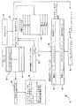
【0025】
図1はコンピュータシステム10の概略図であり、この発明を説明するのに使用される。コンピュータシステム10は、CPU12および14のようなN個のCPUを備える。また、システム10は、メモリコントローラ16およびメインメモリ18を備える。メモリコントローラ16は、エクスポート可能なFETCHADD命令の実行をサポートする。
【0026】
以下にCPU12および14について説明する前に、この発明に従って定義されるFETCHADD命令について最初に述べる。この命令は、以下のフォーマットを持つ。
【数2】
FETCHADD R1=[R3],INC
【0027】
この命令は、レジスタR3のインデックスがついたメモリ位置を読み出し、そのメモリ位置から読み出した内容をレジスタR1に置く。さらに、この命令は、値INCを、そのメモリ位置から読み出した内容に加算し、その和をそのメモリ位置に記憶しなおす。上記のFETCHADD命令の表現は簡略化したものである。追加の命令「コンプリーターズ(completers)」は、メモリから読み出されるべきオペランドのサイズ、他の命令に対するその命令の順序づけセマンティクス(ordering semantics)、およびFETCHADD命令をCPUキャッシュにプリフェッチ(先読み)するときに使用されるプリフェッチヒントなどのようなオプションを指定する。しかしながら、この発明を理解するには上記の命令のフォーマットで充分である。
【0028】
図2は、図1のCPU12のブロック図である。当然ながら、図2は、コンピュータシステム10におけるすべてのCPUを代表する。CPU12には、命令レジスタ20、命令解読実行ロジック22、フォールト・ハンドラー・ポインタ24、プログラムカウンタ26、ソフトウェアベースのIA−32インターセプト・ロックフォールト・ハンドラー28、省略時制御レジスタ(DCR)30、変換索引バッファ(TLB)36、L1およびL2キャッシュメモリ40を備える。図2は概略図であり、この発明を実現するCPUがこれよりも著しく複雑であることは当業者には明らかであろう。しかしながら、図2は、この発明の新規な側面を説明するのには充分である。
【0029】
当該技術分野で知られているように、ほとんどのコンピュータシステムは、実際に存在する物理メモリより多くのメモリがあるようシミュレートする仮想メモリと呼ばれる技術を用いる。メインメモリアドレスに対する仮想アドレスのマッピングは、仮想アドレス変換として知られるプロセスである。仮想アドレスおよび物理アドレス空間は、典型的にはページと呼ばれる等サイズのメモリブロックに分割され、ページテーブルが、仮想アドレスおよび物理アドレスの間の変換を行う。それぞれのページテーブルのエントリは、典型的には物理アドレスと、ページに関する保護および状態情報とを含む。保護および状態情報は、典型的にはページが受けたアクセスの種類についての情報およびページ保護情報を含む。例えば、ダーティビットは、そのページのデータに対して変更が加えられていることを示す。通常、ページテーブルは大きいのでメモリに記憶される。従って、それぞれの規則的なメモリアクセスは、少なくとも2つのアクセスを実際には要求することができ、1つは変換を得るためのものであり、2つめは物理メモリ位置にアクセスするためのものである。
【0030】
仮想アドレス変換をサポートするほとんどのコンピュータシステムは、変換索引バッファ(TLB)を使用する。TLBは、典型的には小容量で高速の連想メモリであり、CPU上またはCPUの近傍に通常は位置し、最近使用された仮想および物理アドレスの対を記憶する。TLBは、ページテーブルにおける変換のサブセットを含み、より高速にアクセスされることができる。処理装置は、メインメモリから情報を必要とするとき、仮想アドレスをTLBに送る。TLBは、仮想アドレスのページ番号を受け取り、物理ページ番号を返す。物理ページ番号は、メインメモリにおける所望のバイトまたはワードをアクセスするため、下位のアドレス情報と組み合わされる。その仮想アドレスの変換がTLBに無いならば、ページテーブルから抽出される。ページテーブルにその変換が無いならば、ページフォールトが生成される。
【0031】
この発明によると、TLB36は、TLBエントリにより表わされるページに対して読み出しおよび書き込みを行うFETCHADD命令を、エクスポート可能であるか否かを決めるメモリアクセスビットを含む。例えば、TLBエントリ38は、メモリアクセスビットフィールド44を含む。上述したように、TLBは通常、ページテーブルに含まれる仮想−物理マッピングのサブセットを含んでいる。従って、この発明で使用するのに適合したページテーブルも、メモリアクセスビットのコピーを含む。
【0032】
表1は、メモリアクセスビットにより表すことができる仮想アドレッシングメモリ属性のコード化を示す。
【表1】

表1に示されるコードは、この発明をよりわかりやすく説明するため簡略化されたものであることに注意されたい。他の実施形態においては、追加の機能性をメモリアクセスビットにコード化するのが望ましいこともある。
【0034】
これらのコードがどのように使用されるのかを説明するため、CPU12、またはCPU12が作動するコンピュータシステムのいずれも、エクスポート可能のFETCHADD命令をサポートしていない場合を想定する。そのようなコンピュータシステムにおいては、原子性は、キャッシュ・コヒーレンシーのアルゴリズムによって提供される。セマフォを含むメモリ位置について仮想−物理マッピングが確立されると、ページテーブルにおけるメモリアクセスビット、およびセマフォが記憶されたページに対応するTLBエントリが、WBのメモリ方式に指定され、従ってメモリアクセスビットが「00」に設定される。
【0035】
従って、FETCHADD命令が命令レジスタ20にロードされると、命令解読実行ロジック22は、FETCHADD命令により指定されたメモリ位置に対応するTLBエントリに記憶されたメモリアクセスビットを調べる。メモリアクセスビットは、ライトバック方式を用いてキャッシュされたメモリページにセマフォが記憶されることを示すので、セマフォを含むキャッシュラインがL1およびL2キャッシュ40にロードされ、専有として保持される。その後、命令解読実行ロジック22は、セマフォをL1キャッシュから抽出し、そのセマフォを、FETCHADD命令中に指定されたレジスタファイル42のレジスタにロードし、セマフォをインクリメントし、インクリメントされたセマフォをL1キャッシュに記憶し直す。セマフォが他のCPUにより要求されるとき、CPU12は、セマフォを含むキャッシュラインの専有使用を放棄し、他のCPUがそのキャッシュラインの専有使用を獲得する。これにより、ある量のキャッシュラインのスラッシングとなるけれども、パフォーマンスは、ローエンドからミドルレンジのコンピュータシステムにおいては充分過ぎると言える。
【0036】
次に、CPU12、およびCPU12が作動するコンピュータシステムの両方が、エクスポート可能なFETCHADD命令をサポートする場合を想定する。そのようなコンピュータシステムにおいては、FETCHADD命令の原子性は、FETCHADD命令をメモリコントローラ(または、その他の中央ロケーション)にエクスポートすることによるか、またはキャッシュ・コヒーレンシー機構によるかのいずれかによって提供することができる。仮想−物理マッピングが、セマフォを含むメモリ位置について確立されるとき、ページテーブルのメモリアクセスビット、およびセマフォが記憶されているページに対応するTLBエントリが、UCEメモリ方式に指定され、従ってメモリアクセスビットは「10」に設定される。
【0037】
従って、FETCHADD命令が命令レジスタ20にロードされるとき、命令解読実行ロジック22は、FETCHADD命令により指定されたメモリ位置に対応するTLBエントリに記憶されたメモリアクセスビットを調べる。メモリアクセスビットは、セマフォが、キャッシュ不可でエクスポート可能なメモリページに記憶されていることを示す。従って、命令解読実行ロジック22は、FETCHADD命令を図1のメモリコントローラ16にエクスポートする。コントローラ16は、図1のメインメモリ18からセマフォを読み出し、そのセマフォを命令解読実行ロジック22に提供し、命令解読実行ロジック22は、FETCHADD命令中に指定されたレジスタファイル42のレジスタにセマフォを記憶する。メモリコントローラ16は、セマフォをインクリメントし、結果をメインメモリ18に記憶しなおす。セマフォがキャッシュラインに専有として保持されることが無いので、他のCPUは、セマフォを含むキャッシュラインの専有使用を得る必要なく、即座にセマフォにアクセスすることができる。従って、キャッシュラインのスラッシングが除去される。メモリコントローラ16が、FETCHADD命令によりアクセスされるセマフォのキャッシュを保持するのが好ましく、これにより、メモリコントローラ16は、メインメモリ18にアクセスする必要がなくなってより速い応答が可能となる点に注意されたい。
【0038】
要約すると、この発明は、原子性がキャッシュ・コヒーレンシー機構により提供されるのか、またはFETCHADD命令をメモリコントローラ16のような中央ロケーションへとエクスポートすることにより提供されるのかを「既製品でシュリンクラップの」ソフトウェアが「知らない」場合でも、該ソフトウェアを、FETCHADD命令によりアクセスされるセマフォでコード化することのできるアーキテクチャ・フレームワークを提供する。従って、このようなソフトウェアは、それぞれの方法について個々のコードセグメントを必要とするソフトウェアなしで、コンピュータハードウェア上で利用可能な原子性更新処理を提供するもっとも高速な方法をアクセスすることができる。
【0039】
この発明により提供される他の利点は、FETCADD命令のエクスポートをサポートするのに、非常に狭い範囲のメモリ位置を選択的にイネーブル(使用可能)にできるということである。従って、オペレーティングシステムは、メモリの小さな部分を、キャッシュ不可でエクスポート可能なよう構成することができ、アプリケーションプログラムが、オペレーティングシステムからセマフォ用のメモリ空間を要求するとき、オペレーティングシステムは、そのような空間を、キャッシュ不可でエクスポート可能なよう構成された領域に割り振ることができる。また、この発明は、オペレーティングシステムが、I/O装置にマッピングされたメモリ位置のような、エクスポート可能なFETCHADD命令をサポートしないメモリ範囲に対するFETCHADD命令のエクスポートを防ぐことができるようにする。
【0040】
この発明は、キャッシュ・コヒーレンシー機構またはFETCHADD命令のエクスポートのいずれかを選択することにより原子性を提供する、64ビットのFETCHADD命令およびそれをサポートするアーキテクチャ・フレームワークを提供するけれども、この発明は、バスロックのプレフィクスを介して原子性を提供するIA−32命令をもサポートする。IA−32命令セットの詳細は、「Intel 命令セットリファレンス」に見つけることができ、ここで参照により取り入れる。
【0041】
IA−32の命令セットにおいて、LOCKプレフィクスは、メモリオペランドにアクセスする形の命令に限り、それらの命令の前に付けることが出来る。すなわち、ADD、ADC、AND、BTC、BTR、BTS、CMPXCHG、DEC、INC、NEG、NOT、OR、SBB、SUB、XOR、XADD、XCHG命令につけることができる。
【0042】
図2を参照すると、省略時制御レジスタ(DCR)30は、IA−32ロックチェック・イネーブルビット(LC)32を含む。LCビット32が「1」に設定され、IA−32の原子的メモリ参照が、外部バスロック下でプロセッサの外部の「読み出し−変更−書き込み」処理を要求する(例えば、命令がLOCKプレフィクスを含む)とき、IA−32インターセプト・ロックフォールトが起こる。LCビット32が「0」にクリアされ、IA−32原子的メモリ参照が、外部バスロック下でプロセッサの外部の「読み出し−変更−書き込み」処理を要求とするとき、プロセッサは、IA−32インターセプト・ロックフォールトを生成するか(バスロックが、コンピュータシステムのハードウェアによりサポートされていない場合)、または外部バスロックでトランザクションを実行することができる。IA−32アーキテクチャにおいては、ライトバックのキャッシュ方式を使用してキャッシュされないメモリに対して行われる原子的メモリアクセスには、外部バスロックが必要となる点に注意されたい。言い換えると、メモリがキャッシュ不可またはライトスルー方式でキャッシュされる場合には、IA−32アーキテクチャには外部バスロックが必要となる。
【0043】
複数の相互接続トポロジーで接続された複数のプロセッサを持つコンピュータシステムのように、バスをロックすることができないコンピュータシステムにおいては、当然ながら、LOCKプレフィクスが前についたIA−32命令は、IA−32インターセプト・ロックフォールトにより取り扱われなければならない。そのようなシステムでは、LCビット32の値は問題とならない。
【0044】
しかしながら、バスをロックすることができるコンピュータシステムを考えてみる。バスをロックすることが可能であるけれども、継続的にそうすることによりパフォーマンスが著しく低下することがある。従って、バスをロックしない命令を使ってLOCKプレフィクスのついたIA−32命令をエミュレートするのが望ましい。エミュレーションは、ハードウェアによって直接実行する程速くはないが、LOCKプレフィクスのついたIA−32命令がエミュレートされる間に他のCPUおよび装置がアクセスを続けることができるので、システム全体のパフォーマンスを上げることができる。このようなシステムにおいては、LOCKプレフィクスのついたIA−32命令が、バスロックを使用してハードウェアにより実行されるのか、またはバスロックを使用せずにソフトウェアでエミュレートされるのかを、LCビット32の値が決定する。LOCKプレフィクスのついたIA−32命令をエミュレートするとき、当然ながら、エミュレーションコードは、キャッシュ・コヒーレンシー機構および/またはエクスポート可能なFETCHADD命令を使用して原子性を確保することができる。
【0045】
図2に戻ると、ADD、ADC、AND、BTC、BTR、BTS、CMPXCHG、DEC、INC、NEG、NOT、OR、SBB、SUB、XOR、XADDおよびXCHGの命令セットからのIA−32命令が、LOCKプレフィクスが前につけられており、メモリ位置をアクセスし、命令レジスタ20にロードされると想定する。さらに、DCR30のLCビット32が「1」に設定されていると想定する。このような命令に応答して、命令解読実行ロジック22は、IA−32インターセプト・ロックフォールトを生成する。ロジック22は、フォールト・ハンドラー・ポインタ24におけるIA−32インターセプト・ロックフォールトエントリ34に記憶されたアドレスを、プログラムカウンタ26にロードする。これにより、フォールト・ハンドラー28の最初の命令が命令レジスタ20にロードされ、ソフトウェアベースのIA−32インターセプト・ロックフォールト・ハンドラー28の最初の命令が実行される。フォールト・ハンドラー28は、割り込みを引き起こしたIA−32命令を調べ、原子的にその命令をエミュレートするため適切なコードへと分岐する。IA−32命令がエミュレートされ、適切な値がレジスタファイル42、L1およびL2キャッシュ40および図1のメインメモリ18に記憶された後、フォールト・ハンドラー28は終了し、フォールトを引き起こした命令のすぐ後の命令を続けて実行する。
【0046】
フォールト・ハンドラー28が、上述したようなエクスポート可能なFETCHADD命令を含むことができる点に注意されたい。例えば、宛先メモリ位置を「1」だけインクリメントするようコード化されたIA−32XADD命令を、「1」に設定されたインクリメント値(INC)を持つFETCHADD命令によりエミュレートすることができる。FETCHADD命令によりエミュレートすることのできない他の命令については、変更されるべきメモリ位置を含むキャッシュラインの専有使用を得る命令によりエミュレートすることができる。
【0047】
要約すると、DCR30のLCビット32およびソフトウェアベースのIA−32インターセプト・ロックフォールト・ハンドラー28により、CPU12は、バスをロックすることなくLOCKプレフィクスのついたIA−32命令を原子的に実行することができるようになる。従って、この発明により、64ビットのアーキテクチャを持つコンピュータシステムは、64ビットのアーキテクチャにより提供される優れたパフォーマンスを維持しつつ、IA−32命令との2値互換性を維持することができるようになる。
【0048】
この発明を、好ましい実施形態を参照しつつ説明してきたけれども、当該技術分野の当業者には、この発明の精神および範囲から離れること無く、形式および詳細において変更を加えることができるということが明らかであろう。
【発明の効果】
特定の原子的更新方法を利用するようソフトウェアを明確にコード化することなく、ソフトウェアは、ハードウェアにより提供される最高のパフォーマンスの原子的更新方法をアクセスできるようになる。
【図面の簡単な説明】
【図1】N個のCPU、メモリコントローラおよびメインメモリを備えるコンピュータシステムの概略図。
【図2】この発明による、図1のCPUのうちの1つのブロック図。
【符号の説明】
12、14 CPU
16 メモリコントローラ
18 メインメモリ
36 TLB
44 メモリ属性フィールド[0001]
BACKGROUND OF THE INVENTION
The present invention relates to a memory access operation in a computer system. More specifically, the present invention relates to an atomic memory update process that is typically used to access a semaphore.
[0002]
[Prior art]
In a computer system, two or more processes often compete for the same resource. For example, two or more processes may attempt to write a specific command sequence to the video controller. These processes may be executed by a single central processing unit (CPU) or may be executed by two or more CPUs of a multiprocessor computer system. Here, the terms “CPU” and “processor” are used interchangeably.
[0003]
Since multiple processes cannot access a resource at the same time, the computer operating system must provide some mechanism for scheduling access to the resource. One common mechanism known in the art is the “take-a-number” scheduling algorithm. This algorithm is somewhat similar to a group of customers waiting for one store clerk to open. The customer receives a number when entering the store. When the clerk calls the number, the customer can receive the clerk's service.
[0004]
Analogous to this, the mechanism for providing a “number” to a process is known in the art as a semaphore. Typically, semaphores are stored in memory locations. A process attempting to access a semaphore first reads a memory location, increments the value read from this memory location, and stores the result back in that memory location. The value read from the memory location serves as the “number” for that process, and the result stored back to the memory location serves as the next “number” for the next process that tries to access the resource. Fulfill. When the operating system indicates that a holder of a particular “number” may access the resource, the process with that “number” performs the access.
[0005]
In order for the “number acquisition” scheduling algorithm to operate correctly, memory read, increment and memory write operations must occur “atomic”. In other words, the second process reads the memory location holding the semaphore from the time when the first process reads the memory location until the time when the first process stores the incremented value back into the memory location. There should be no opportunity. If such a read operation by the second process occurs, the first and second processes will each have the same “number” and may attempt to access the resource simultaneously.
[0006]
Ensuring that semaphore operations occur atomically is relatively simple in a single CPU computer system where no other device connected to the bus performs direct memory access (DMA) processing. . For example, the 32-bit Intel ™ architecture (IA-32) is Intel i486. TM , Pentium (TM), Pentium Pro, Pentium II and Celeron TM And includes an "XADD (exchange and add)" instruction. When using this instruction to access a memory location containing a semaphore, the XADD instruction is typically used as follows.
XADD Destination memory location, source register
[0007]
This instruction stores the sum of the values contained in the destination memory location and the source register in a temporary register, stores the contents of the destination memory location in the source register, and stores the contents of the temporary register in the destination memory location. Thus, if the value “1” is stored in the source register when the instruction is executed, the value of the destination memory location is incremented by “1” when the instruction is completed, and the value originally in the destination memory location is Stored in the source register. Interrupts are not processed until the instruction completes, and since the computer system in this example is a single CPU (other devices do not perform DMA processing), the "read-" executed by the XADD instruction No other process can access the semaphore during the "read-modify-write" process. Therefore, semaphore processing occurs atomically. The IA-32 XCHG (exchange) and CMPXCHG (compare and exchange) instructions are also widely used to ensure atomic access to semaphores.
[0008]
In a system with a multiprocessor computer system and a device that performs DMA processing, the second CPU or device attempts to access the semaphore before the first CPU increments and writes the semaphore back to the memory location As a result, it is more complicated to guarantee atomicity. In such computer systems, atomicity is provided by using either a bus locking mechanism or a cache coherency mechanism. Before describing these mechanisms in detail, it is useful to first consider the processing of the CPU cache memory.
[0009]
A cache memory is a relatively small and fast memory that holds a subset of the contents of the main memory. For example, a computer system based on a Pentium ™ II CPU has a level 1 (L1) cache on the same integrated circuit (IC) as the CPU, and a level 2 (L2) cache as the CPU. They are on the same module but on different ICs. The L1 cache is smaller and faster than the L2 cache. The contents of the main memory are stored in the cache memory in units called cache lines. In the Pentium II CPU, the cache line size of the L1 and L2 caches is 32 bytes.
[0010]
Intel (TM) i486 TM CPU employs a “write-through” L1 cache. In such a cache, memory writes from the CPU are simultaneously written into the cache and main memory. Since the Intel Pentium CPU, Intel processors support "write-back" caching. In the write-back cache, memory writes from the CPU are written only to the cache. The cache mechanism then determines whether (and when) the memory write was actually committed to main memory. As a result, writing to the main memory can be delayed until the main memory is not busy, thereby improving performance (performance). In addition, the memory operand may change several times before the memory operand is written back to main memory. Also, before the cache line is written back to memory, the cache is given the opportunity to fully assemble the cache line changes, which is known in the art as coalescing.
[0011]
The cache coherency mechanism ensures that the memory contents stored in the CPU cache and main memory are kept coherent. For example, the cache of the first CPU includes a cache line with modified (ie, “dirty”) content that has not yet been written back to main memory, and the second CPU When attempting to read the corresponding memory location from memory, the cache coherency mechanism ensures that the correct content from the cache of the first CPU is not the incorrect content currently stored in main memory, Provided to the CPU. A cache coherency mechanism can accomplish this in several ways. One approach is simply to force the first CPU cache to write the modified cache line back to main memory. Another approach is to make changes in the cache of the first CPU by allowing the second CPU's cache to “snoop” changes to the first CPU's cache. The cache of the second CPU can be continuously updated.
[0012]
Further, the CPU can request that the cache line be loaded as “shared” or “exclusive”. Shared cache lines cannot be changed by the CPU and are therefore advantageously used in situations where it is known that the contents of the cache line will not change (eg, program code). A dedicated (or alternatively referred to as “private”) cache line can be changed by the CPU. Typically, a “dirty-bit” is associated with a proprietary cache line and indicates whether the contents have changed. If the dirty bit is set, indicating that the cache line has changed, the cache line must be written back to main memory. If the dirty bit is cleared, indicating that the cache line has not been modified, the cache line can be discarded as written back to main memory. Normally, at any one time, only one CPU can hold a specific cache line as exclusive.
[0013]
Returning to atomicity, the early IA-32 CPU stored the semaphore in non-cacheable memory or cached memory using write-through methods, and when accessing the semaphore, "bus lock (Bus lock) "to issue atomicity. The bus lock ensures that one CPU has exclusive ownership of the bus during "read-modify-write" transactions required by semaphore processing. In this way, all other CPUs can access the bus until the “read-modify-write” transaction is completed, even if no other CUP needs to access the memory area containing the semaphore. Will be a heavy burden on performance. In high-end multiprocessor systems that use various interconnect structures, the concept of “bus” may disappear completely, and therefore the concept of “bus lock” may also disappear completely. Please be careful. For example, in a multiprocessor system having a pod of four processors, each processor in one pod being coupled via a conventional bus, and each pod interconnected in a ring topology: The CPU in one pod is usually unable to lock the bus in the other pod.
[0014]
The later IA-32 CPU provides atomicity via a cache coherency mechanism. When the CPU accesses a semaphore, the CPU's L1 cache requests exclusive use of the cache line that includes the memory location holding the semaphore. Thus, the CPU can execute a “read-modify-write” transaction required by semaphore processing without the possibility of other CPUs accessing the semaphore during the transaction. Accordingly, other CPUs can continue to access the bus, and therefore can continue to access the memory. Since only the main memory area that is not accessible to other CPUs is a cache line that is held exclusively in the cache of the CPU executing the semaphore process, it is essentially an “in-cache” atom. Update is performed via an “address lock”. Note that it is often desirable not to store multiple semaphores in one cache line, since the entire cache line is held as exclusive.
[0015]
This provision of atomicity through cache coherency provides much better performance than providing cache coherence through bus locks, but performance is still limited by "thrashing of semaphore cache lines" There is. Semaphore cache line thrashing occurs when two or more CPUs continuously contend for the same resource, and therefore the same semaphore. Therefore, each CPU continuously attempts to obtain exclusive control of the cache line including the semaphore, and the cache line is continuously loaded and written into the cache of each CPU. Normally, while a CPU is waiting to obtain exclusive access to a cache line including a semaphore, the processing of that CPU cannot proceed.
[0016]
In the prior art, some large multiprocessor systems have addressed this problem using FETCHADD (fetch and add) instructions. The “increment” process associated with the “FETCHADD” instruction is exported to a central location, such as a memory controller. Thus, when the CPU executes a FETCHADD instruction that references a semaphore stored at a memory location, the memory controller provides the CPU with the semaphore value stored at the memory location. In addition, the memory controller increments the semaphore and stores the result back to that memory location. Thus, since the CPU does not need to write to the memory location containing the semaphore, the CPU does not need to gain exclusive access to the cache line containing the semaphore, thereby eliminating thrashing of the semaphore cache line. In addition, since multiple semaphores can exist within the boundary of the cache line without sacrificing performance, the semaphores can be stored in memory more efficiently.
[0017]
[Problems to be solved by the invention]
In the computer industry, there is an active movement towards higher performance hardware. However, as opposed to this, a wide variety of hardware, including bus locks designed to provide atomic semaphore updates, cache coherency mechanisms, and hardware architectures that provide atomicity through instruction export There is also a tendency to aggressively move towards lower-cost “off-the-shelf shrink-wrapped” operating systems (and other software) that can run on hardware architectures. However, prior art methods of providing atomicity usually assume that the software “recognizes” how atomicity is provided. Thus, software designed to access semaphores using bus locks uses cache coherency mechanisms designed to provide atomic semaphore updates, and higher semaphore performance provided by instruction export. I can't. Similarly, software designed to access semaphores using a cache coherency mechanism may use the higher semaphore performance provided by instruction exports designed to provide atomic semaphore updates. Can not. What is needed in the art is that low-cost “off-the-shelf shrink-wrapped” software can be implemented in a computer system on which it is executed without the need to explicitly code the software to utilize a specific atomic update method. A computer architecture that allows access to the best performing atomic update method provided by the hardware.
[0018]
[Means for Solving the Problems]
In order to solve the above problem, the present invention includes a step of accessing a memory attribute field to determine whether a memory location accessed by an atomic update process supports an exportable instruction; If the memory location accessed by the local update process supports exportable instructions, the step of exporting the atomic update process to a central location and the memory location accessed by the atomic update process can be exported If the instruction is not supported, a method for performing an atomic update process is provided that includes using a cache coherency mechanism to perform the atomic update process.
The present invention provides a 64-bit architectural framework such that IA-32 instructions requiring bus locks execute efficiently on computer hardware providing an excellent way to provide atomicity. Is. Furthermore, the present invention provides an architectural framework that defines an exportable 64-bit FETCHADD (fetch and add) instruction that can be coded into "off-the-shelf shrink wrap" software and export instructions. Or by using a cache coherency mechanism to provide a programmable way for hardware to ensure atomicity in executing FETCHADD instructions.
[0019]
In the IA-32 instruction set, the LOCK prefix can be prepended to instructions that only access memory operands. That is, it can be placed before the ADD, ADC, AND, BTC, BTR, BTS, CMPXCHG, DEC, INC, NEG, NOT, OR, SBB, SUB, XOR, XADD, and XCHG instructions. In accordance with the present invention, the CPU includes a default control register including an IA-32 lock check enable bit (LC). The LC bit is set to “1” and the IA-32 atomic memory reference requires a “read-modify-write” process external to the processor under external bus lock (eg, the instruction IA-32 intercept lock fault fault occurs and the IA-32 intercept lock fault handler is called. The fault handler examines the IA-32 instruction that caused the interrupt and branches to the appropriate code to atomically emulate the instruction. Accordingly, the present invention allows a computer system having a 64-bit architecture according to the present invention to maintain binary (binary) compatibility with IA-32 instructions, and by not locking the bus, To maintain the excellent performance provided by the architecture of.
[0020]
In addition, the present invention defines an exportable FETCHADD instruction having the following format:
[Expression 1]
FETCHADD R 1 = [R 3 ], INC
[0021]
This instruction uses register R 3 Read out the memory location indexed by and stores the contents read from that memory location in register R 1 , Add the INC value to the contents read from that memory location, and store the sum back in that memory location.
[0022]
Associated with each virtual memory page may be in a state of “cacheable using write-back method (WB)”, “cannot be cached (UC)”, or “cannot be cached and can be exported (UCE)”. Memory attribute. When the FETCHADD instruction is executed and the accessed memory location is on a page with the attribute set in WB, the FETCHADD instruction is executed atomically by the CPU by obtaining exclusive use of the cache line containing that memory location Is done. However, when a FETCHADD instruction is executed and the accessed memory location is on a page with attributes set to UCE, the FETCHADD instruction is exported by exporting it to a central location such as a memory controller. Performed atomically, thereby eliminating semaphore cache line thrashing.
[0023]
Thus, the present invention allows software to be “unaware” whether atomicity is provided by a cache coherency mechanism or by exporting FETCHADD instructions to a central location such as a memory controller. Provides an architectural framework that can code "off-the-shelf and shrink-wrapped" software with semaphores accessed by the FETCHADD instruction. Thus, such software can access the fastest method that provides an atomic update process available on computer hardware, without software requiring individual code segments for each method. it can.
[0024]
DETAILED DESCRIPTION OF THE INVENTION
The present invention provides a 64-bit architectural framework that efficiently executes IA-32 instructions that require a bus lock on computer hardware that provides an excellent way to provide cache coherence. Furthermore, the present invention uses an architecture that defines an exportable 64-bit FETCHADD instruction that can be encoded into "off-the-shelf shrink wrap" software, and by exporting the instruction or using a cache coherency mechanism. This provides a programmable way in which hardware can guarantee atomicity in executing the FETCHADD instruction.
[0025]
FIG. 1 is a schematic diagram of a
[0026]
Before describing
[Expression 2]
FETCHADD R 1 = [R 3 ], INC
[0027]
This instruction uses register R 3 Is read from the memory location, and the contents read from the memory location are stored in the register R. 1 Put on. In addition, this instruction adds the value INC to the contents read from the memory location and stores the sum back in the memory location. The above expression of the FETCHADD instruction is simplified. The additional instruction "completers" is used to prefetch the FETCHADD instruction into the CPU cache, the size of the operands to be read from memory, the ordering semantics of the instruction relative to other instructions Specify options such as prefetch hints to be played. However, the above instruction format is sufficient to understand the present invention.
[0028]
FIG. 2 is a block diagram of the
[0029]
As is known in the art, most computer systems use a technique called virtual memory that simulates having more memory than actual physical memory. The mapping of virtual addresses to main memory addresses is a process known as virtual address translation. The virtual address and physical address space is typically divided into equally sized memory blocks called pages, and the page table translates between virtual and physical addresses. Each page table entry typically includes a physical address and protection and status information about the page. Protection and status information typically includes information about the type of access the page has received and page protection information. For example, the dirty bit indicates that a change has been made to the data of the page. Usually, the page table is large and is stored in the memory. Thus, each regular memory access can actually require at least two accesses, one for obtaining a translation and the second for accessing a physical memory location. is there.
[0030]
Most computer systems that support virtual address translation use a translation index buffer (TLB). A TLB is typically a small-capacity, high-speed associative memory, usually located on or near the CPU, and stores recently used virtual and physical address pairs. The TLB includes a subset of translations in the page table and can be accessed faster. When the processor needs information from the main memory, it sends a virtual address to the TLB. The TLB receives the page number of the virtual address and returns the physical page number. The physical page number is combined with the lower address information to access the desired byte or word in main memory. If the virtual address translation does not exist in the TLB, it is extracted from the page table. If the page table does not have that translation, a page fault is generated.
[0031]
In accordance with the present invention,
[0032]
Table 1 shows the encoding of virtual addressing memory attributes that can be represented by memory access bits.
[Table 1]
Note that the codes shown in Table 1 have been simplified to better illustrate the present invention. In other embodiments, it may be desirable to encode additional functionality into memory access bits.
[0034]
To illustrate how these codes are used, assume that neither
[0035]
Thus, when the FETCHADD instruction is loaded into the
[0036]
Next, assume that both
[0037]
Thus, when the FETCHADD instruction is loaded into the
[0038]
In summary, the present invention describes whether "atomicity is provided by a cache coherency mechanism or by exporting FETCHADD instructions to a central location such as the
[0039]
Another advantage provided by the present invention is that a very narrow range of memory locations can be selectively enabled to support the export of FETCADD instructions. Thus, the operating system can be configured so that a small portion of memory is non-cacheable and exportable, and when an application program requests memory space for a semaphore from the operating system, the operating system Can be allocated to an area that is configured to be non-cacheable and exportable. The invention also enables the operating system to prevent the export of FETCHADD instructions for memory ranges that do not support exportable FETCHADD instructions, such as memory locations mapped to I / O devices.
[0040]
Although the present invention provides a 64-bit FETCHADD instruction and an architecture framework that supports it, which provides atomicity by choosing either a cache coherency mechanism or an export of the FETCHADD instruction, It also supports IA-32 instructions that provide atomicity via a bus lock prefix. Details of the IA-32 instruction set can be found in the "Intel Instruction Set Reference", here incorporated by reference.
[0041]
In the IA-32 instruction set, the LOCK prefix can be prefixed to instructions that only access memory operands. That is, it can be attached to ADD, ADC, AND, BTC, BTR, BTS, CMPXCHG, DEC, INC, NEG, NOT, OR, SBB, SUB, XOR, XADD, and XCHG instructions.
[0042]
Referring to FIG. 2, the default control register (DCR) 30 includes an IA-32 lock check enable bit (LC) 32. The
[0043]
Of course, in a computer system that cannot lock the bus, such as a computer system with multiple processors connected in multiple interconnect topologies, an IA-32 instruction preceded by a LOCK prefix is IA- Must be handled by 32 intercept lock faults. In such a system, the value of
[0044]
However, consider a computer system that can lock the bus. Although it is possible to lock the bus, doing so continuously can severely degrade performance. Therefore, it is desirable to emulate an IA-32 instruction with a LOCK prefix using an instruction that does not lock the bus. Emulation is not fast enough to be performed directly by hardware, but system-wide performance is possible because other CPUs and devices can continue to access while IA-32 instructions with a LOCK prefix are emulated. Can be raised. In such a system, whether an IA-32 instruction with a LOCK prefix is executed by hardware using a bus lock or emulated in software without using a bus lock, The value of
[0045]
Returning to FIG. 2, IA-32 instructions from the ADD, ADC, AND, BTC, BTR, BTS, CMPXCHG, DEC, INC, NEG, NOT, OR, SBB, SUB, XOR, XADD and XCHG instruction sets Assume that the LOCK prefix is prefixed, accessing the memory location and loaded into the
[0046]
Note that the
[0047]
In summary, the
[0048]
Although the invention has been described with reference to preferred embodiments, it will be apparent to those skilled in the art that changes can be made in form and detail without departing from the spirit and scope of the invention. Will.
【The invention's effect】
Without explicitly coding the software to utilize a particular atomic update method, the software will be able to access the best performing atomic update method provided by the hardware.
[Brief description of the drawings]
FIG. 1 is a schematic diagram of a computer system including N CPUs, a memory controller, and a main memory.
2 is a block diagram of one of the CPUs of FIG. 1 in accordance with the present invention.
[Explanation of symbols]
12, 14 CPU
16 Memory controller
18 Main memory
36 TLB
44 Memory attribute field
Claims (6)
エクスポート可能なフェッチおよび加算(FETCHADD)命令を受け取ることが可能な命令レジスタと、
仮想対物理メモリ変換を記憶する複数のエントリを有する変換索引バッファ(TLB)であって、それぞれの該エントリは、該エントリに記憶された該仮想対物理メモリ変換に関連付けられた物理ページが、ライトバックのメモリ方式をサポートするのか、または、キャッシュ不可であるがエクスポート可能なメモリ方式をサポートするのか、を示すメモリアクセスビットを含む、変換索引バッファと、
前記変換索引バッファおよび前記外部のメモリコントローラとの間に接続されたキャッシュメモリと、
前記命令レジスタ、前記外部のメモリコントローラ、および前記変換索引バッファに接続された、命令を解読して実行する命令解読実行ロジックと、を備え、
前記命令解読実行ロジックは、前記エクスポート可能なフェッチおよび加算命令により示される目標メモリ位置に対応する該変換索引バッファのエントリのメモリ属性を調べることにより、該エクスポート可能なフェッチおよび加算命令を実行し、該目標メモリ位置が前記ライトバックのメモリ方式をサポートすることを該メモリ属性が示すならば、該目標メモリ位置のコピーを含むキャッシュラインが、「排他」なコヒーレンシ状態で前記キャッシュメモリにロードされると共に、前記エクスポート可能なフェッチおよび加算命令は、該キャッシュメモリに記憶された該目標メモリ位置のコピーを使用して完了され、前記目標メモリ位置が前記キャッシュ不可であるがエクスポート可能なメモリ方式であることを前記メモリ属性が示すならば、該エクスポート可能なフェッチおよび加算命令は、前記外部のメモリコントローラによって実行されるために該メモリコントローラにエクスポートされる、
中央処理装置。A central processing unit that can be connected to an external memory controller,
An instruction register capable of receiving exportable fetch and add (FETCHADD) instructions; and
A translation index buffer (TLB) having a plurality of entries for storing virtual-to-physical memory translations, each entry having a physical page associated with the virtual-to-physical memory translation stored in the entry A translation index buffer that includes a memory access bit that indicates whether to support a back-memory scheme or a non-cacheable but exportable memory scheme;
A cache memory connected between the conversion index buffer and the external memory controller;
Instruction decoding execution logic connected to the instruction register, the external memory controller, and the conversion index buffer for decoding and executing an instruction;
The instruction decode execution logic executes the exportable fetch and add instruction by examining the memory attribute of the entry of the translation index buffer corresponding to the target memory location indicated by the exportable fetch and add instruction; If the memory attribute indicates that the target memory location supports the write-back memory scheme, a cache line containing a copy of the target memory location is loaded into the cache memory in an “exclusive” coherency state. And the exportable fetch and add instructions are completed using a copy of the target memory location stored in the cache memory, wherein the target memory location is the non-cacheable but exportable memory scheme. If the memory attribute indicates that , The exportable fetch and add instruction, is exported to the memory controller to be executed by the external memory controller,
Central processing unit.
前記中央処理装置は、さらに、
ソフトウェアベースのバスロック・フォールト・ハンドラーのルーチンを指す割り込みハンドラー・ポインターと、
ロックチェック・イネーブルビットを有する省略時制御レジスタと、を備え、
前記命令解読実行ロジックは、前記ロックチェック・イネーブルビットがセットされている時、該バスロックのプレフィックスが付いた前記命令をエミュレートするソフトウェアベースの前記バスロック・フォールト・ハンドラーのルーチンを実行し、前記ロックチェック・イネーブルビットがセットされていない時、該中央処理装置を前記外部のメモリコントローラに接続するバスをロックすることにより、該バスロックのプレフィックスが付いた前記命令を実行する、
請求項1に記載の中央処理装置。The instruction register, it is possible to receive an instruction with a prefix of the bus lock,
The central processing unit further includes:
An interrupt handler pointer that points to the routine of the software-based buslock fault handler;
A default control register having a lock check enable bit, and
The instruction decode execution logic, when said lock check enable bit is set, executes the routines of the software-based said bus lock fault handler to emulate the instruction with prefix of said bus lock and, when the lock check enable bit is not set, by locking the bus connecting the central processing unit to said external memory controller to execute the instructions prefixed of said bus lock,
The central processing unit according to claim 1.
バスロックのプレフィックスが付いた命令を受け取ることができる命令レジスタと、
ソフトウェアベースのバスロック・フォールト・ハンドラーのルーチンを指す割り込みハンドラーのポインタと、
ロックチェック・イネーブルビットを有する省略時制御レジスタと、
前記命令レジスタ、前記外部のメモリコントローラ、前記割り込みハンドラーのポインタ、および前記省略時制御レジスタに接続され、命令を解読して実行する命令解読実行ロジックと、を備え、
前記ロジックは、前記ロックチェック・イネーブルビットがセットされている時は、該バスロックのプレフィックスが付いた前記命令をエミュレートする前記ソフトウェアベースのバスロック・フォールト・ハンドラーのルーチンを実行し、前記ロックチェック・イネーブルビットがセットされていない時は、該中央処理装置を前記外部のメモリコントローラに接続するバスをロックすることにより、該バスロックのプレフィックスが付いた前記命令を実行する、
中央処理装置。A central processing unit capable of being connected to an external memory controller,
And the instruction register instruction can receive that with a prefix of the bus lock,
An interrupt handler pointer to the software-based buslock fault handler routine;
A default control register having a lock check enable bit;
An instruction decoding execution logic connected to the instruction register, the external memory controller, the pointer of the interrupt handler, and the default control register to decode and execute an instruction;
The logic is, when the lock check enable bit is set, executes the routines of the software-based bus lock fault handler to emulate the instruction with prefix of said bus lock, when the lock check enable bit is not set, by locking the bus connecting the central processing unit to said external memory controller to execute the instructions marked with prefix of said bus lock,
Central processing unit.
仮想対物理メモリ変換を記憶する複数のエントリを有する変換索引バッファ(TLB)であって、それぞれの該エントリは、該エントリに記憶された該仮想対物理メモリ変換に関連付けられた物理ページが、ライトバックのメモリ方式をサポートするのか、または、キャッシュ不可であるがエクスポート可能なメモリ方式をサポートするのか、を示すメモリアクセスビットを含む、変換索引バッファと、
前記変換索引バッファおよび前記外部のメモリコントローラとの間に接続されたキャッシュメモリと、を備え、
前記命令解読実行ロジックは、前記変換索引バッファに接続されており、該ロジックは、前記エクスポート可能なフェッチおよび加算命令により示される目標メモリ位置に対応する該変換索引バッファのエントリのメモリ属性を調べることによって、該エクスポート可能なフェッチおよび加算命令を実行し、該目標メモリ位置が前記ライトバックのメモリ方式をサポートすることを該メモリ属性が示すならば、該目標メモリ位置のコピーを含むキャッシュラインが、排他として前記キャッシュメモリにロードされると共に、該エクスポート可能なフェッチおよび加算命令は、該キャッシュメモリに記憶された該目標メモリ位置のコピーを使用して完了され、前記目標メモリ位置がキャッシュ不可であるがエクスポート可能なメモリ方式であることを該メモリ属性が示すならば、該エクスポート可能なフェッチおよび加算命令は、前記外部のメモリコントローラによって実行されるために該メモリコントローラにエクスポートされる、
請求項3に記載の中央処理装置。The instruction register can receive an exportable fetch and add (FETCHADD) instruction, the central processing unit further comprising:
A translation index buffer (TLB) having a plurality of entries for storing virtual-to-physical memory translations, each entry having a physical page associated with the virtual-to-physical memory translation stored in the entry A translation index buffer that includes a memory access bit that indicates whether to support a back-memory scheme or a non-cacheable but exportable memory scheme;
A cache memory connected between the conversion index buffer and the external memory controller ,
The instruction decode execution logic is coupled to the translation index buffer, and the logic examines a memory attribute of an entry in the translation index buffer corresponding to a target memory location indicated by the exportable fetch and add instructions. To execute the exportable fetch and add instructions, and if the memory attribute indicates that the target memory location supports the write-back memory scheme, a cache line containing a copy of the target memory location is: Loaded into the cache memory as exclusive and the exportable fetch and add instructions are completed using a copy of the target memory location stored in the cache memory, and the target memory location is non-cacheable Is an exportable memory method If preparative indicated the memory attribute, the exportable fetch and add instruction, is exported to the memory controller to be executed by the external memory controller,
The central processing unit according to claim 3.
メインメモリユニットと、
前記メインメモリユニットに接続されたメモリコントローラであって、エクスポート可能なフェッチおよび加算命令を受け取って実行することができるメモリコントローラと、
前記メモリコントローラに接続された複数の中央処理装置と、を備え、それぞれの該中央処理装置は、
エクスポート可能なフェッチおよび加算命令を受け取ることが可能な命令レジスタと、
仮想対物理メモリ変換を記憶する複数のエントリを有する変換索引バッファ(TLB)であって、それぞれの該エントリは、該エントリに記憶された該仮想対物理メモリ変換に関連付けられた物理ページが、ライトバックのメモリ方式をサポートするのか、または、キャッシュ不可であるがエクスポート可能なメモリ方式をサポートするのか、を示すメモリアクセスビットを含む、変換索引バッファと、
前記変換索引バッファおよび前記外部のメモリコントローラとの間に接続されたキャッシュメモリと、
前記命令レジスタ、前記外部のメモリコントローラ、および前記変換索引バッファに接続された、命令を解読して実行する命令解読実行ロジックと、を備え、
前記ロジックは、前記エクスポート可能なフェッチおよび加算命令により示される目標メモリ位置に対応する該変換索引バッファのエントリのメモリ属性を調べることによって、該エクスポート可能なフェッチおよび加算命令を実行し、該目標メモリ位置が前記ライトバックのメモリ方式をサポートすることを、該メモリ属性が示すならば、該目標メモリ位置のコピーを含むキャッシュラインが、排他として前記キャッシュメモリにロードされると共に、前記エクスポート可能なフェッチおよび加算命令は、該キャッシュメモリに記憶された該目標メモリ位置のコピーを使用して完了され、前記目標メモリ位置がキャッシュ不可であるがエクスポート可能なメモリ方式であることを、該メモリ属性が示すならば、該エクスポート可能なフェッチおよび加算命令は、前記外部のメモリコントローラによって実行されるために該メモリコントローラにエクスポートされる、
マルチプロセッサコンピュータシステム。A multiprocessor computer system,
A main memory unit;
A memory controller connected to the main memory unit, capable of receiving and executing exportable fetch and add instructions;
A plurality of central processing units connected to the memory controller , each of the central processing units,
An instruction register capable of receiving exportable fetch and add instructions; and
A translation index buffer (TLB) having a plurality of entries for storing virtual-to-physical memory translations, each entry having a physical page associated with the virtual-to-physical memory translation stored in the entry A translation index buffer that includes a memory access bit that indicates whether to support a back-memory scheme or a non-cacheable but exportable memory scheme;
A cache memory connected between the conversion index buffer and the external memory controller;
Instruction decoding execution logic connected to the instruction register, the external memory controller, and the conversion index buffer for decoding and executing an instruction;
The logic executes the exportable fetch and add instruction by examining a memory attribute of an entry in the translation index buffer corresponding to a target memory location indicated by the exportable fetch and add instruction, If the memory attribute indicates that a location supports the write-back memory scheme, a cache line containing a copy of the target memory location is loaded into the cache memory as an exclusive and the exportable fetch And the add instruction is completed using a copy of the target memory location stored in the cache memory and the memory attribute indicates that the target memory location is a non-cacheable but exportable memory scheme The exportable fes And addition instructions are exported to the memory controller to be executed by the external memory controller,
Multiprocessor computer system.
ソフトウェアベースのバスロック・フォールト・ハンドラーのルーチンを指す割り込みハンドラーのポインタと、
ロックチェック・イネーブルビットを有する省略時制御レジスタと、を備え、
前記命令解読実行ロジックは、前記ロックチェック・イネーブルビットがセットされている時は、該バスロックのプレフィックスが付いた前記命令をエミュレートする前記ソフトウェアベースのバスロック・フォールト・ハンドラーのルーチンを実行し、前記ロックチェック・イネーブルビットがセットされていない時は、該中央処理装置を前記外部のメモリコントローラに接続するバスをロックすることにより、該バスロックのプレフィックスが付いた前記命令を実行する、
請求項5に記載のマルチプロセッサコンピュータシステム。The instruction register of each of the central processing units can receive instructions prefixed with a bus lock, each central processing unit further comprising:
An interrupt handler pointer to the software-based buslock fault handler routine;
A default control register having a lock check enable bit, and
The instruction decode execution logic executes the software-based bus lock fault handler routine that emulates the instruction with the bus lock prefix when the lock check enable bit is set. When the lock check enable bit is not set, the instruction with the bus lock prefix is executed by locking the bus connecting the central processing unit to the external memory controller;
The multiprocessor computer system according to claim 5.
Applications Claiming Priority (2)
| Application Number | Priority Date | Filing Date | Title |
|---|---|---|---|
| US170137 | 1998-10-12 | ||
| US09/170,137 US6430657B1 (en) | 1998-10-12 | 1998-10-12 | Computer system that provides atomicity by using a tlb to indicate whether an exportable instruction should be executed using cache coherency or by exporting the exportable instruction, and emulates instructions specifying a bus lock |
Publications (3)
| Publication Number | Publication Date |
|---|---|
| JP2000122916A JP2000122916A (en) | 2000-04-28 |
| JP2000122916A5 JP2000122916A5 (en) | 2006-11-16 |
| JP4531890B2 true JP4531890B2 (en) | 2010-08-25 |
Family
ID=22618690
Family Applications (1)
| Application Number | Title | Priority Date | Filing Date |
|---|---|---|---|
| JP28666099A Expired - Fee Related JP4531890B2 (en) | 1998-10-12 | 1999-10-07 | How to perform an atomic update process |
Country Status (2)
| Country | Link |
|---|---|
| US (1) | US6430657B1 (en) |
| JP (1) | JP4531890B2 (en) |
Families Citing this family (43)
| Publication number | Priority date | Publication date | Assignee | Title |
|---|---|---|---|---|
| US6341338B1 (en) * | 1999-02-04 | 2002-01-22 | Sun Microsystems, Inc. | Protocol for coordinating the distribution of shared memory |
| US6587964B1 (en) * | 2000-02-18 | 2003-07-01 | Hewlett-Packard Development Company, L.P. | Transparent software emulation as an alternative to hardware bus lock |
| US6802057B1 (en) | 2000-05-03 | 2004-10-05 | Sun Microsystems, Inc. | Automatic generation of fortran 90 interfaces to fortran 77 code |
| US6986130B1 (en) | 2000-07-28 | 2006-01-10 | Sun Microsystems, Inc. | Methods and apparatus for compiling computer programs using partial function inlining |
| US6594736B1 (en) * | 2000-08-15 | 2003-07-15 | Src Computers, Inc. | System and method for semaphore and atomic operation management in a multiprocessor |
| US6804741B2 (en) * | 2002-01-16 | 2004-10-12 | Hewlett-Packard Development Company, L.P. | Coherent memory mapping tables for host I/O bridge |
| US7971030B2 (en) * | 2002-08-07 | 2011-06-28 | Mmagix Technology Limited | Method for using multiple processing resources which share multiple co-processor resources |
| US7146607B2 (en) * | 2002-09-17 | 2006-12-05 | International Business Machines Corporation | Method and system for transparent dynamic optimization in a multiprocessing environment |
| US7496494B2 (en) * | 2002-09-17 | 2009-02-24 | International Business Machines Corporation | Method and system for multiprocessor emulation on a multiprocessor host system |
| US8108843B2 (en) * | 2002-09-17 | 2012-01-31 | International Business Machines Corporation | Hybrid mechanism for more efficient emulation and method therefor |
| US9043194B2 (en) * | 2002-09-17 | 2015-05-26 | International Business Machines Corporation | Method and system for efficient emulation of multiprocessor memory consistency |
| US7953588B2 (en) * | 2002-09-17 | 2011-05-31 | International Business Machines Corporation | Method and system for efficient emulation of multiprocessor address translation on a multiprocessor host |
| US7103528B2 (en) * | 2002-09-19 | 2006-09-05 | Lsi Logic Corporation | Emulated atomic instruction sequences in a multiprocessor system |
| US7917646B2 (en) * | 2002-12-19 | 2011-03-29 | Intel Corporation | Speculative distributed conflict resolution for a cache coherency protocol |
| US7130969B2 (en) * | 2002-12-19 | 2006-10-31 | Intel Corporation | Hierarchical directories for cache coherency in a multiprocessor system |
| US7636815B1 (en) * | 2003-04-09 | 2009-12-22 | Klaiber Alexander C | System and method for handling direct memory accesses |
| US8751753B1 (en) | 2003-04-09 | 2014-06-10 | Guillermo J. Rozas | Coherence de-coupling buffer |
| US20040263386A1 (en) * | 2003-06-26 | 2004-12-30 | King Thomas M. | Satellite positioning system receivers and methods |
| US20050071606A1 (en) * | 2003-09-30 | 2005-03-31 | Roman Talyansky | Device, system and method of allocating spill cells in binary instrumentation using one free register |
| US7822929B2 (en) | 2004-04-27 | 2010-10-26 | Intel Corporation | Two-hop cache coherency protocol |
| US20050262250A1 (en) * | 2004-04-27 | 2005-11-24 | Batson Brannon J | Messaging protocol |
| US20050240734A1 (en) * | 2004-04-27 | 2005-10-27 | Batson Brannon J | Cache coherence protocol |
| US9280473B2 (en) | 2004-12-02 | 2016-03-08 | Intel Corporation | Method and apparatus for accessing physical memory from a CPU or processing element in a high performance manner |
| US7971002B1 (en) * | 2005-04-07 | 2011-06-28 | Guillermo Rozas | Maintaining instruction coherency in a translation-based computer system architecture |
| US7814292B2 (en) * | 2005-06-14 | 2010-10-12 | Intel Corporation | Memory attribute speculation |
| US7676796B2 (en) * | 2005-09-29 | 2010-03-09 | Intel Corporation | Device, system and method for maintaining a pre-defined number of free registers within an instrumented program |
| US7991965B2 (en) * | 2006-02-07 | 2011-08-02 | Intel Corporation | Technique for using memory attributes |
| US7487279B2 (en) * | 2007-01-23 | 2009-02-03 | International Business Machines Corporation | Achieving both locking fairness and locking performance with spin locks |
| US9032100B2 (en) * | 2008-04-03 | 2015-05-12 | International Business Machines Corporation | I/O hub-supported atomic I/O operations |
| US8275598B2 (en) * | 2009-03-02 | 2012-09-25 | International Business Machines Corporation | Software table walk during test verification of a simulated densely threaded network on a chip |
| US8793471B2 (en) | 2010-12-07 | 2014-07-29 | Advanced Micro Devices, Inc. | Atomic program verification |
| US9122476B2 (en) | 2010-12-07 | 2015-09-01 | Advanced Micro Devices, Inc. | Programmable atomic memory using hardware validation agent |
| US8788794B2 (en) | 2010-12-07 | 2014-07-22 | Advanced Micro Devices, Inc. | Programmable atomic memory using stored atomic procedures |
| CN103064375B (en) * | 2012-12-18 | 2015-01-14 | 国核电站运行服务技术有限公司 | Control method of remote control upper computer for nuclear-level device detecting |
| US9058282B2 (en) | 2012-12-31 | 2015-06-16 | Intel Corporation | Dynamic cache write policy |
| US10078613B1 (en) | 2014-03-05 | 2018-09-18 | Mellanox Technologies, Ltd. | Computing in parallel processing environments |
| US9558115B2 (en) * | 2014-04-22 | 2017-01-31 | Netapp, Inc. | Write-back caching-based atomicity in a distributed storage system |
| WO2016064403A1 (en) * | 2014-10-23 | 2016-04-28 | Hewlett Packard Enterprise Development Lp | Supervisory memory management unit |
| FR3048526B1 (en) * | 2016-03-07 | 2023-01-06 | Kalray | ATOMIC INSTRUCTION LIMITED IN RANGE AT AN INTERMEDIATE CACHE LEVEL |
| US10402218B2 (en) * | 2016-08-30 | 2019-09-03 | Intel Corporation | Detecting bus locking conditions and avoiding bus locks |
| US10394653B1 (en) | 2017-05-02 | 2019-08-27 | Mellanox Technologies, Ltd. | Computing in parallel processing environments |
| US10528519B2 (en) | 2017-05-02 | 2020-01-07 | Mellanox Technologies Ltd. | Computing in parallel processing environments |
| US10394747B1 (en) | 2017-05-31 | 2019-08-27 | Mellanox Technologies Ltd. | Implementing hierarchical PCI express switch topology over coherent mesh interconnect |
Family Cites Families (8)
| Publication number | Priority date | Publication date | Assignee | Title |
|---|---|---|---|---|
| JPH04340144A (en) * | 1991-05-17 | 1992-11-26 | Nec Corp | Bus lock control device |
| US5428761A (en) * | 1992-03-12 | 1995-06-27 | Digital Equipment Corporation | System for achieving atomic non-sequential multi-word operations in shared memory |
| US5535365A (en) * | 1993-10-22 | 1996-07-09 | Cray Research, Inc. | Method and apparatus for locking shared memory locations in multiprocessing systems |
| US5535352A (en) * | 1994-03-24 | 1996-07-09 | Hewlett-Packard Company | Access hints for input/output address translation mechanisms |
| US5574922A (en) * | 1994-06-17 | 1996-11-12 | Apple Computer, Inc. | Processor with sequences of processor instructions for locked memory updates |
| US5761731A (en) * | 1995-01-13 | 1998-06-02 | Digital Equipment Corporation | Method and apparatus for performing atomic transactions in a shared memory multi processor system |
| US6519623B1 (en) * | 1996-10-31 | 2003-02-11 | International Business Machines Corporation | Generic semaphore for concurrent access by multiple operating systems |
| US5895495A (en) * | 1997-03-13 | 1999-04-20 | International Business Machines Corporation | Demand-based larx-reserve protocol for SMP system buses |
-
1998
- 1998-10-12 US US09/170,137 patent/US6430657B1/en not_active Expired - Lifetime
-
1999
- 1999-10-07 JP JP28666099A patent/JP4531890B2/en not_active Expired - Fee Related
Also Published As
| Publication number | Publication date |
|---|---|
| US6430657B1 (en) | 2002-08-06 |
| JP2000122916A (en) | 2000-04-28 |
Similar Documents
| Publication | Publication Date | Title |
|---|---|---|
| JP4531890B2 (en) | How to perform an atomic update process | |
| US9804970B2 (en) | Invalidating a range of two or more translation table entries and instruction therefor | |
| JP4136001B2 (en) | Computing system for I / O address translation mechanism | |
| US7228389B2 (en) | System and method for maintaining cache coherency in a shared memory system | |
| US8452942B2 (en) | Invalidating a range of two or more translation table entries and instruction therefore | |
| US9304916B2 (en) | Page invalidation processing with setting of storage key to predefined value | |
| US6901505B2 (en) | Instruction causing swap of base address from segment register with address from another register | |
| US6456891B1 (en) | System and method for transparent handling of extended register states | |
| US8521964B2 (en) | Reducing interprocessor communications pursuant to updating of a storage key | |
| US5555395A (en) | System for memory table cache reloads in a reduced number of cycles using a memory controller to set status bits in the main memory table | |
| US8918601B2 (en) | Deferred page clearing in a multiprocessor computer system | |
| JPH0997214A (en) | Information-processing system inclusive of address conversion for auxiliary processor | |
| US8458438B2 (en) | System, method and computer program product for providing quiesce filtering for shared memory | |
| EP0669579A2 (en) | Coherence index generation for use by an input/output adapter | |
| US7310712B1 (en) | Virtual copy system and method | |
| JPH04251352A (en) | Selective locking of memory position in on-chip cache of microprocessor | |
| EP0173909B1 (en) | Look-aside buffer least recently used marker controller | |
| JP2000339221A (en) | System and method for invalidating entry of conversion device | |
| CN113885943A (en) | Processing unit, system on chip, computing device and method | |
| EP0389886A2 (en) | Ring reduction logic mechanism | |
| CN113641403A (en) | Microprocessor and method implemented in microprocessor | |
| Dixon | Page associative caches on Futurebus | |
| Curley et al. | Hardware differences in the 9373 and 9375 processors |
Legal Events
| Date | Code | Title | Description |
|---|---|---|---|
| A521 | Written amendment |
Free format text: JAPANESE INTERMEDIATE CODE: A523 Effective date: 20061003 |
|
| A621 | Written request for application examination |
Free format text: JAPANESE INTERMEDIATE CODE: A621 Effective date: 20061003 |
|
| A131 | Notification of reasons for refusal |
Free format text: JAPANESE INTERMEDIATE CODE: A131 Effective date: 20091117 |
|
| A601 | Written request for extension of time |
Free format text: JAPANESE INTERMEDIATE CODE: A601 Effective date: 20100113 |
|
| A602 | Written permission of extension of time |
Free format text: JAPANESE INTERMEDIATE CODE: A602 Effective date: 20100118 |
|
| A521 | Written amendment |
Free format text: JAPANESE INTERMEDIATE CODE: A523 Effective date: 20100414 |
|
| TRDD | Decision of grant or rejection written | ||
| A01 | Written decision to grant a patent or to grant a registration (utility model) |
Free format text: JAPANESE INTERMEDIATE CODE: A01 Effective date: 20100512 |
|
| A01 | Written decision to grant a patent or to grant a registration (utility model) |
Free format text: JAPANESE INTERMEDIATE CODE: A01 |
|
| A61 | First payment of annual fees (during grant procedure) |
Free format text: JAPANESE INTERMEDIATE CODE: A61 Effective date: 20100610 |
|
| R150 | Certificate of patent or registration of utility model |
Ref document number: 4531890 Country of ref document: JP Free format text: JAPANESE INTERMEDIATE CODE: R150 Free format text: JAPANESE INTERMEDIATE CODE: R150 |
|
| FPAY | Renewal fee payment (event date is renewal date of database) |
Free format text: PAYMENT UNTIL: 20130618 Year of fee payment: 3 |
|
| R250 | Receipt of annual fees |
Free format text: JAPANESE INTERMEDIATE CODE: R250 |
|
| R250 | Receipt of annual fees |
Free format text: JAPANESE INTERMEDIATE CODE: R250 |
|
| R250 | Receipt of annual fees |
Free format text: JAPANESE INTERMEDIATE CODE: R250 |
|
| R250 | Receipt of annual fees |
Free format text: JAPANESE INTERMEDIATE CODE: R250 |
|
| R250 | Receipt of annual fees |
Free format text: JAPANESE INTERMEDIATE CODE: R250 |
|
| R250 | Receipt of annual fees |
Free format text: JAPANESE INTERMEDIATE CODE: R250 |
|
| LAPS | Cancellation because of no payment of annual fees |