JP4530961B2 - Electronic image stabilization device - Google Patents
Electronic image stabilization device Download PDFInfo
- Publication number
- JP4530961B2 JP4530961B2 JP2005278748A JP2005278748A JP4530961B2 JP 4530961 B2 JP4530961 B2 JP 4530961B2 JP 2005278748 A JP2005278748 A JP 2005278748A JP 2005278748 A JP2005278748 A JP 2005278748A JP 4530961 B2 JP4530961 B2 JP 4530961B2
- Authority
- JP
- Japan
- Prior art keywords
- image
- unit
- time
- blur
- exposure
- Prior art date
- Legal status (The legal status is an assumption and is not a legal conclusion. Google has not performed a legal analysis and makes no representation as to the accuracy of the status listed.)
- Expired - Fee Related
Links
Images


Classifications
-
- H—ELECTRICITY
- H04—ELECTRIC COMMUNICATION TECHNIQUE
- H04N—PICTORIAL COMMUNICATION, e.g. TELEVISION
- H04N23/00—Cameras or camera modules comprising electronic image sensors; Control thereof
- H04N23/60—Control of cameras or camera modules
- H04N23/68—Control of cameras or camera modules for stable pick-up of the scene, e.g. compensating for camera body vibrations
- H04N23/682—Vibration or motion blur correction
- H04N23/684—Vibration or motion blur correction performed by controlling the image sensor readout, e.g. by controlling the integration time
- H04N23/6845—Vibration or motion blur correction performed by controlling the image sensor readout, e.g. by controlling the integration time by combination of a plurality of images sequentially taken
Description
本発明は、固体撮像素子に結像される画像のぶれを電子的に補正する電子的ぶれ補正装置に関する。 The present invention relates to an electronic shake correction apparatus that electronically corrects a shake of an image formed on a solid-state imaging device.
固体撮像素子を用いて静止画像や動画像を撮像する撮像装置は、手で把持して撮影するように構成されたものが少なくない。このような撮像装置において、例えば被写体の輝度が低い場合には、シャッタ速度が遅くなるために、手ぶれが発生し易くなることが知られている。また、車載カメラ等においては、走行時の振動により、同様にぶれが発生する可能性があることが知られている。 Many imaging devices that capture a still image or a moving image using a solid-state imaging device are configured to be captured by hand. In such an imaging apparatus, for example, when the luminance of a subject is low, it is known that camera shake is likely to occur because the shutter speed becomes slow. In addition, it is known that in-vehicle cameras and the like may be shaken similarly due to vibration during traveling.
こうしたぶれを補正するための技術は、従来より種々のものが提案されており、その代表的な例の幾つかについて、以下に説明する。 Various techniques for correcting such blurring have been proposed, and some typical examples will be described below.
(1)電子式ぶれ補正(特開平6−46316号公報等)
電子式ぶれ補正では、有効画素領域を、撮像素子を用いて撮像可能な最大の画素領域よりもかなり小さめの領域にしておく。そして、電子式ぶれ補正機能を搭載したデジタルカメラで撮影を行ったときには、撮影された画像は、直ちにメモリカードに記録されるのではなく、まず一時的にバッファメモリに記憶される。デジタルカメラは、時間的間隔を離すことなくすぐに次の画像を撮影する。この2番目に撮影された画像も、1番目に撮影された画像と同様に、直ちにメモリカードに記録されるのではなく、まずバッファメモリに記憶される。このとき、2番目に撮影した画像における被写体の位置が、最初に撮影した画像における被写体の位置とずれてしまった(ぶれてしまった)場合には、デジタルカメラは、1枚目の画像と2枚目の画像とを比較して、被写体が同様の構図で画面の中に納まるように使用するデータ領域をずらし、これを2番目の画像における有効画素領域とする。このような技術を用いることにより、各画像間での被写体の位置がずれることのない(つまり、画像間のぶれが発生することのない)画像データを記録することが可能となる。
(1) Electronic blur correction (Japanese Patent Laid-Open No. 6-46316, etc.)
In the electronic blur correction, the effective pixel area is set to an area considerably smaller than the maximum pixel area that can be imaged using the image sensor. Then, when shooting is performed with a digital camera equipped with an electronic blur correction function, the shot image is not temporarily recorded on the memory card, but temporarily temporarily stored in the buffer memory. The digital camera captures the next image immediately without leaving a time interval. Similarly to the first photographed image, the second photographed image is not immediately recorded on the memory card but is first stored in the buffer memory. At this time, if the position of the subject in the second photographed image is shifted (blurred) from the position of the subject in the first photographed image, the digital camera detects that the first image and 2 Compared with the first image, the data area to be used is shifted so that the subject fits in the screen with the same composition, and this is used as the effective pixel area in the second image. By using such a technique, it is possible to record image data in which the position of the subject does not shift between the images (that is, no blur occurs between the images).
(2)光学式ぶれ補正(特開平10−336510号公報等)
光学式ぶれ補正では、振動ジャイロがカメラの移動を感知すると、光が届く位置のぶれを打ち消す方向にレンズの一部を動かす方式が主流である。このような技術を用いることにより、カメラが動いてぶれが発生しそうになっても、シャッタが開いた後に最初に撮像素子に届いた光の位置と、シャッタが閉じる寸前に撮像素子に届いた光の位置と、を同一の位置にして、ぶれを防ぐことが可能となる。
(2) Optical blur correction (JP-A-10-336510, etc.)
In the optical shake correction, when the vibration gyroscope senses the movement of the camera, the mainstream method is to move a part of the lens in a direction to cancel the shake at the position where the light reaches. By using such technology, even if the camera is likely to move and shake, the position of the light that first reaches the image sensor after the shutter opens and the light that reaches the image sensor just before the shutter closes. It is possible to prevent the camera shake by setting the same position to the same position.
(3)センサーシフト式ぶれ補正(特開2004−56581号公報)
センサーシフト式ぶれ補正は、振動ジャイロがカメラの移動を感知すると、撮像面における光の到達位置のぶれ量だけ撮像素子を移動することにより、ぶれを補正する技術である。この技術は、レンズの一部が移動することがないために、画質の劣化を基本的に伴うことなく、ぶれ補正を行うことができる利点がある。そして、この技術は、レンズ交換式のカメラにおけるカメラ本体側に適用することが可能であるために、ぶれ補正の技術が考慮されていない従来の交換レンズを用いても、ぶれ補正を行うことができる利点がある。
(3) Sensor shift type blur correction (Japanese Patent Laid-Open No. 2004-56581)
The sensor shift type shake correction is a technique for correcting the shake by moving the image sensor by the shake amount of the light arrival position on the imaging surface when the vibration gyroscope senses the movement of the camera. This technique has an advantage that blur correction can be performed without basically deteriorating image quality because a part of the lens does not move. Since this technology can be applied to the camera body side of an interchangeable lens camera, it is possible to perform blur correction even using a conventional interchangeable lens that does not consider the blur correction technology. There are advantages you can do.
(4)特開2001−86398号公報
この公報に記載された撮像装置は、ぶれが発生しない露光時間間隔で撮影した複数の画像を、撮像素子から読み出してバッファメモリに記憶しておき、このバッファメモリに記憶された複数の画像の相互の像ぶれ(相互の像位置のずれ)を補正した後に、この補正された各画像を加算することによりぶれのない画像を生成するものとなっている。この技術は、電子的にぶれ補正を行うものであるために、複雑なメカニカル機構が不要になる利点がある。
(4) Japanese Patent Laid-Open No. 2001-86398 The image pickup apparatus described in this publication reads a plurality of images taken at exposure time intervals at which no blurring occurs from the image pickup device and stores them in a buffer memory. After correcting the image blur (mutual image position shift) of the plurality of images stored in the memory, the corrected images are added to generate an image without blur. This technique has an advantage that a complicated mechanical mechanism is not required because the electronic shake correction is performed electronically.
ところで、特開平8−148667号公報には、光導電膜積層型の固体撮像素子が記載されている。この技術を用いた光導電膜積層型のCCDは、水平走査および垂直走査を行うCCD上に、光電変換および変換された電荷の蓄積を行う光導電膜を積層し、さらに、この光導電膜に透明電極を積層したものとなっている。
しかしながら、上述したような電子式ぶれ補正の技術は、複数の画像データを連続してみたときに構図や被写体位置がぶれたりしないようにする技術であって、1枚の画像内においてのみ発生しているぶれを補正する技術とはなっていない。つまり、各1枚毎の画像が例えば露光時間が長いことにより手ぶれしたとしても、その手ぶれを抑制する技術とはなっておらず、静止画におけるぶれ補正にそのまま有効に適用できる技術とはいえない。 However, the electronic blur correction technique as described above is a technique for preventing the composition and the subject position from blurring when a plurality of image data are continuously viewed, and occurs only in one image. It is not a technology that corrects shaking. That is, even if each image is shaken due to, for example, a long exposure time, it is not a technique for suppressing the shake, and cannot be said to be a technique that can be effectively applied as it is to shake correction in a still image. .
一方、上述したような光学式ぶれ補正は、静止画におけるぶれ補正に適用可能であるが、設計が大変に難しく、コストが高いものとなっている。また、ぶれは補正されるものの、例えば色収差が幾らか増大してしまい、厳密に見ると、光学性能の劣化が発生してしまうことになる。さらに、電子式ぶれ補正の技術と異なって、レンズを移動する機構を組み込む必要があるために、該機構を組み込んだデジタルカメラ等は、小型化を図るのが難しくなる。加えて、この技術を例えばレンズ交換式のカメラに適用すると、ぶれ補正機構の少なくとも一部をレンズ側に組み込むことが必要になるために、従来のぶれ補正機能に対応していない交換レンズでは、ぶれ補正を行うことができない。 On the other hand, the optical blur correction as described above can be applied to the blur correction in a still image, but the design is very difficult and the cost is high. In addition, although the blur is corrected, for example, chromatic aberration is somewhat increased, and strictly speaking, optical performance is deteriorated. Further, unlike the electronic blur correction technique, it is necessary to incorporate a mechanism for moving the lens, so that it is difficult to reduce the size of a digital camera or the like incorporating the mechanism. In addition, when this technology is applied to, for example, an interchangeable lens camera, it is necessary to incorporate at least a part of the blur correction mechanism on the lens side. Therefore, in an interchangeable lens that does not support the conventional blur correction function, Camera shake cannot be corrected.
また、上述したようなセンサーシフト式ぶれ補正は、機構的に撮像素子を駆動するものであるために、該機構を組み込んだデジタルカメラ等の小型化を図るのが難しくなるのは、上述した光学式ぶれ補正の場合と同様である。また、撮像素子が大きい場合には、移動量も大きくなるために、機構が大型化するのは避けられない。そして、撮像素子は、撮影レンズの光軸に対して垂直な撮像平面上でのみ移動することが重要になるが、ガタの発生や、光軸に対する撮像素子の傾き、光軸周りの撮像素子の回転などを防止するのは、困難である。 In addition, since the sensor shift type blur correction as described above mechanically drives the image sensor, it is difficult to reduce the size of a digital camera or the like incorporating the mechanism. This is the same as in the case of formula blur correction. In addition, when the image sensor is large, the amount of movement is large, and thus the mechanism is inevitably increased in size. It is important for the image sensor to move only on the imaging plane perpendicular to the optical axis of the photographic lens. However, the occurrence of backlash, the tilt of the image sensor with respect to the optical axis, the image sensor around the optical axis, It is difficult to prevent rotation and the like.
さらに、上記特開2001−86398号公報に記載された技術は、1枚の画像データを得るために、撮像素子から複数回の読み出しを行う必要がある。この撮像素子からの読み出しは、撮像素子を構成する画素数が多いほど長い時間を要する。具体的な例を挙げると、600万画素の撮像素子から30[MHz]の周期で画素信号を読み出す場合には、全画素の信号を1回読み出すだけで200[ms]の時間を要することになる。従って、複数回の読み出しを行う場合には、この200[ms]の整数倍の時間(もしくはそれ以上の時間)を要することになる。一方、例えば35mmフィルムカメラにおいては、撮影レンズの焦点距離をf[mm]としたときに、ぶれの発生を概略抑制し得る最長露光時間が1/f[秒]であるということが経験的に知られている。例えば、標準的な50[mm]の撮影レンズを用いる場合には、この最長露光時間は20[ms]となる。しかし、上記撮像素子から画像信号を1回読み出す時間200[ms]でさえも、この最長露光時間20[ms]に比べて極めて長くなってしまうために、ましてや複数回の読み出しを行うのは時間的に長くなり過ぎる。こうして、該公報に記載された技術は、例えば、撮像素子の画素数が少なく、かつ、ぶれの発生を概略抑制し得る最長露光時間が長い(例えば、撮影レンズの焦点距離が短い)というような、限られた条件においてのみ実用的であると考えられる。 Furthermore, the technique described in the above-mentioned Japanese Patent Application Laid-Open No. 2001-86398 needs to read a plurality of times from the image sensor in order to obtain one piece of image data. The readout from the image sensor requires a longer time as the number of pixels constituting the image sensor increases. As a specific example, in the case where pixel signals are read out from a 6-million-pixel imaging device at a cycle of 30 [MHz], it takes 200 [ms] to read out signals of all pixels once. Become. Therefore, when reading is performed a plurality of times, an integral multiple of 200 [ms] (or more) is required. On the other hand, in a 35 mm film camera, for example, when the focal length of the photographic lens is f [mm], the longest exposure time that can substantially suppress the occurrence of blurring is empirically 1 / f [second]. Are known. For example, when a standard 50 [mm] photographing lens is used, the longest exposure time is 20 [ms]. However, even the time 200 [ms] for reading the image signal once from the image sensor becomes extremely longer than the longest exposure time 20 [ms]. Too long. Thus, for example, the technique described in the publication discloses that the number of pixels of the image sensor is small, and the longest exposure time that can substantially suppress the occurrence of blurring is long (for example, the focal length of the photographing lens is short). It is considered practical only under limited conditions.
こうして、メカニカル機構を不要としながら、幅広いシャッタスピードに対応したぶれ補正を可能とする電子的ぶれ補正装置、異なる時刻に得られた複数の画像を高速に加算することができる固体撮像素子が望まれていた。 Thus, there is a demand for an electronic shake correction device that enables shake correction corresponding to a wide range of shutter speeds without requiring a mechanical mechanism, and a solid-state imaging device that can quickly add a plurality of images obtained at different times. It was.
本発明は上記事情に鑑みてなされたものであり、メカニカル機構を不要としながら、幅広いシャッタスピードに対応したぶれ補正を可能とする電子的ぶれ補正装置を提供することを目的としている。 SUMMARY OF THE INVENTION The present invention has been made in view of the above circumstances, and an object thereof is to provide an electronic shake correction apparatus that enables shake correction corresponding to a wide range of shutter speeds without requiring a mechanical mechanism.
上記の目的を達成するために、第1の発明による電子的ぶれ補正装置は、マトリクス状に配列された複数の画素を有する固体撮像素子の撮像面に結像される画像のぶれを補正して、ぶれの補正された画像を生成するための電子的ぶれ補正装置であって、上記固体撮像素子の撮像面に像を結像するための撮像光学系と、上記画像のぶれを検出するぶれ検出部と、上記固体撮像素子の露光量を制御する露光量制御部と、上記露光量制御部の制御に基づき上記固体撮像素子により所定の露光量で複数の画像を撮影する撮像部と、上記撮像部により撮影された第1画像を第1方向に沿った画素行単位で記憶するとともに該第1画像を該第1方向に転送する第1転送レジスタと、上記第1画像とは異なる時刻に撮影された第2画像を上記第1方向と直交する第2方向に沿った画素列単位で記憶するとともに該第2画像を該第2方向に転送する第2転送レジスタと、上記第1画像及び上記第2画像をそれぞれ上記第1転送レジスタ及び上記第2転送レジスタ内で相対的にシフトした後に加算して、上記第1転送レジスタ又は上記第2転送レジスタ内に記憶する加算部と、上記加算部により加算された画素の電荷を上記固体撮像素子から読み出す読出部と、を具備し、上記第1転送レジスタと上記第2転送レジスタとを、互いに交差して格子状となるように、かつ互いの交差箇所において転送レジスタを共有するように、形成したものである。 In order to achieve the above object, an electronic blur correction apparatus according to a first invention corrects blurring of an image formed on an imaging surface of a solid-state imaging device having a plurality of pixels arranged in a matrix. An electronic shake correction apparatus for generating a shake-corrected image, an imaging optical system for forming an image on an imaging surface of the solid-state imaging device, and a shake detection for detecting the shake of the image An exposure amount control unit that controls the exposure amount of the solid-state imaging device, an imaging unit that captures a plurality of images with a predetermined exposure amount based on the control of the exposure amount control unit, and the imaging a first transfer register for transferring the first image to the first direction stores the first image captured in units of pixel row along the first direction by the part, taken at different times from the above first image orthogonal to the second image having the above first direction That second transfer register for transferring the second image to the second direction and stores pixel column basis in the second direction, the first image and the second image, respectively the first transfer register and the An addition unit which adds after being relatively shifted in the second transfer register and stores in the first transfer register or the second transfer register, and the charge of the pixel added by the addition unit is the solid-state imaging device A first reading register and a second transfer register formed so as to intersect with each other in a lattice shape and to share the transfer register at each intersection. It is a thing.
また、第2の発明による電子的ぶれ補正装置は、上記第1の発明による電子的ぶれ補正装置において、上記加算部が、時間的に相前後して撮影された2つの画像の相対的なぶれを補正してから上記2つの画像をアナログ的に加算し、さらにこの加算した画像とその次に撮影した画像との相対的なぶれを補正してからこれら2つの画像をアナログ的に加算するという動作を繰り返し行うように制御するものである。 According to a second aspect of the present invention, in the electronic shake correction apparatus according to the first aspect of the present invention, the adding unit is configured to detect a relative blur between two images taken in time series. The above two images are added in an analog manner after correcting the image, and the two images are added in an analog manner after correcting the relative blurring between the added image and the next photographed image. It controls to repeat the operation.
さらに、第3の発明による電子的ぶれ補正装置は、上記第2の発明による電子的ぶれ補正装置において、上記加算部が、上記撮影された複数の画像の内の最初の画像の撮影における露光開始から最新の画像の撮影における露光終了までの画像のぶれ量と、該複数の画像の内の最初の画像から最新の1つ前の画像までのぶれ補正量の累積加算値と、の差に基いて、最新の画像と既に加算した画像とのぶれを補正して、ぶれを補正したこれら2つの画像をアナログ的に加算するように制御するものである。 Furthermore, the electronic shake correction apparatus according to the third invention is the electronic shake correction apparatus according to the second invention, wherein the adding unit starts exposure in taking the first image among the plurality of taken images. Based on the difference between the image blur amount from the first image to the end of exposure in the shooting of the latest image and the cumulative added value of the blur correction amount from the first image to the latest previous image of the plurality of images. Then, blurring between the latest image and the already added image is corrected, and control is performed so that these two images corrected for blurring are added in an analog manner.
第4の発明による電子的ぶれ補正装置は、上記第1の発明による電子的ぶれ補正装置において、上記露光量制御部が、ぶれを許容し得るようなぶれ限界露光時間以下の予め設定された露光時間で所定回数の露光を上記固体撮像素子に行わせるように制御するものである。 According to a fourth aspect of the present invention, there is provided an electronic shake correction apparatus according to the first aspect of the present invention, wherein the exposure amount control unit has a preset exposure that is not more than a blur limit exposure time that allows the shake to be allowed. Control is performed so that the solid-state image sensor is exposed a predetermined number of times over time.
第5の発明による電子的ぶれ補正装置は、上記第4の発明による電子的ぶれ補正装置において、上記露光量制御部が、撮像光学系の焦点距離の情報に基いて、上記ぶれ限界露光時間を生成するものである。 According to a fifth aspect of the present invention, in the electronic blur correction device according to the fourth aspect of the invention, the exposure amount control unit sets the blur limit exposure time based on information on a focal length of the imaging optical system. Is to be generated.
第6の発明による電子的ぶれ補正装置は、上記第4の発明による電子的ぶれ補正装置において、上記ぶれ検出部が、露光開始前においてもぶれ量の演算を行うものであり、上記露光量制御部は、露光開始前に上記ぶれ量検出部により演算したぶれ量が許容可能なぶれ量の上限に達するまでの露光時間を演算し、この露光時間に基づいて上記ぶれ限界露光時間を生成するものである。 An electronic shake correction apparatus according to a sixth invention is the electronic shake correction apparatus according to the fourth invention, wherein the shake detection unit calculates a shake amount even before the start of exposure. The unit calculates an exposure time until the blur amount calculated by the blur amount detection unit reaches an upper limit of an allowable blur amount before the start of exposure, and generates the blur limit exposure time based on the exposure time. It is.
第7の発明による電子的ぶれ補正装置は、上記第4の発明による電子的ぶれ補正装置において、上記露光量制御部が、露光時に上記ぶれ量演算部により演算したぶれ量が許容可能なぶれ量の上限に達するまでの露光時間を演算し、この露光時間に基づいて上記ぶれ限界露光時間を生成するものである。 An electronic shake correction apparatus according to a seventh aspect of the present invention is the electronic shake correction apparatus according to the fourth aspect of the invention, wherein the amount of shake that the exposure amount control unit calculates by the shake amount calculation unit during exposure is allowable. The exposure time until the upper limit is reached is calculated, and the blur limit exposure time is generated based on this exposure time.
第8の発明による電子的ぶれ補正装置は、上記第1の発明による電子的ぶれ補正装置において、上記露光量制御部が、被写体の明るさを取得する測光部と、上記測光部により取得された被写体の明るさに基づき適正露光を得るための第1露光時間を生成する第1露光時間生成部と、第2露光時間を生成する第2露光時間生成部と、上記第2露光時間で連続して予め定められた撮影回数の撮影を行ったときの露光時間の合計が上記第1露光時間に等しくなるように制御する露光時間制御部と、を備えたものである。 An electronic shake correction apparatus according to an eighth aspect of the present invention is the electronic shake correction apparatus according to the first aspect of the invention, wherein the exposure amount control unit is acquired by a photometry unit that acquires the brightness of a subject and the photometry unit. A first exposure time generation unit that generates a first exposure time for obtaining an appropriate exposure based on the brightness of the subject, a second exposure time generation unit that generates a second exposure time, and the second exposure time. And an exposure time control unit that controls the exposure time when the predetermined number of times of shooting are performed to be equal to the first exposure time.
第9の発明による電子的ぶれ補正装置は、上記第8の発明による電子的ぶれ補正装置において、上記連続して撮影する予め定められた撮影回数を記憶するメモリをさらに具備し、上記露光時間制御部は、上記第1露光時間を上記撮影回数により割って得られた時間を第2露光時間として生成させるように上記第2露光時間生成部を制御するものである。 An electronic shake correction apparatus according to a ninth aspect of the invention is the electronic shake correction apparatus according to the eighth aspect of the invention, further comprising a memory for storing the predetermined number of times of continuous shooting, wherein the exposure time control is performed. The unit controls the second exposure time generation unit so that a time obtained by dividing the first exposure time by the number of photographing times is generated as a second exposure time.
第10の発明による電子的ぶれ補正装置は、上記第9の発明による電子的ぶれ補正装置において、上記第2露光時間生成部により生成された上記第2露光時間が、ぶれを許容可能なレベルに抑制し得る露光時間より長いときは、ぶれが発生する可能性があることを示す警告表示を行う表示部をさらに具備したものである。 An electronic shake correction apparatus according to a tenth aspect of the invention is the electronic shake correction apparatus according to the ninth aspect of the invention, wherein the second exposure time generated by the second exposure time generation unit is at a level that allows shake. When it is longer than the exposure time that can be suppressed, it further includes a display unit that displays a warning indicating that there is a possibility of blurring.
第11の発明による電子的ぶれ補正装置は、上記第8の発明による電子的ぶれ補正装置において、上記連続して撮影する予め定められた撮影回数として選択可能な複数の撮影回数を記憶するメモリをさらに具備し、上記露光時間制御部は、上記メモリに記憶されている撮影回数の中から、上記第1露光時間を上記第2露光時間で割った値以上の該値に最も近い整数を撮影回数として選択し、上記第1露光時間を上記撮影回数により割って得られた時間を上記第2露光時間に代えて新たな第2露光時間として生成させるように上記第2露光時間生成部を制御するものである。 An electronic shake correction apparatus according to an eleventh aspect of the invention is the electronic shake correction apparatus according to the eighth aspect of the invention, wherein a memory for storing a plurality of shooting times that can be selected as the predetermined number of shooting times for continuous shooting is provided. The exposure time control unit further includes an integer closest to the value equal to or greater than a value obtained by dividing the first exposure time by the second exposure time from the number of times stored in the memory. And the second exposure time generator is controlled so that a time obtained by dividing the first exposure time by the number of times of photographing is generated as a new second exposure time instead of the second exposure time. Is.
第12の発明による電子的ぶれ補正装置は、上記第8の発明による電子的ぶれ補正装置において、上記撮像光学系は絞りを有して構成されたものであって、当該電子的ぶれ補正装置は、上記撮像光学系の絞り値を設定する絞り値設定部と、上記連続して撮影する撮影回数を記憶するメモリと、をさらに具備し、上記絞り値設定部は、上記第1露光時間が、上記第2露光時間と、上記メモリに記憶されている撮影回数の内の最大値と、の積である第3露光時間よりも長いときには、該第1露光時間が該第3露光時間以下になるように上記撮像光学系の絞り値を変更するものである。 An electronic shake correction apparatus according to a twelfth aspect of the invention is the electronic shake correction apparatus according to the eighth aspect of the invention, wherein the imaging optical system is configured with a stop, and the electronic shake correction apparatus is And an aperture value setting unit for setting an aperture value of the imaging optical system, and a memory for storing the number of times of continuous shooting, wherein the aperture value setting unit includes the first exposure time, When the second exposure time is longer than the third exposure time, which is the product of the maximum number of photographings stored in the memory, the first exposure time is equal to or shorter than the third exposure time. As described above, the aperture value of the imaging optical system is changed.
第13の発明による電子的ぶれ補正装置は、上記第12の発明による電子的ぶれ補正装置において、上記絞り値設定部により上記撮像光学系の絞り値を変更するときにはその旨を表示する表示部をさらに具備したものである。 An electronic shake correction apparatus according to a thirteenth aspect of the present invention is the electronic shake correction apparatus according to the twelfth aspect of the present invention, wherein a display unit for displaying the fact is displayed when the aperture value setting unit changes the aperture value of the imaging optical system. Furthermore, it is equipped.
第14の発明による電子的ぶれ補正装置は、上記第12の発明による電子的ぶれ補正装置において、上記撮像素子から得られる画像の増幅率を変更することにより実質的にISO感度を変更するためのISO感度変更部をさらに具備し、上記ISO感度変更部は、上記絞り値設定部が変更しようとする絞り値が、上記撮像光学系の絞り値として設定可能な範囲を逸脱しているときには、該設定可能な範囲内に入るようにISO感度を変更するものである。 An electronic shake correction apparatus according to a fourteenth aspect of the invention is the electronic shake correction apparatus according to the twelfth aspect of the invention, wherein the ISO sensitivity is substantially changed by changing an amplification factor of an image obtained from the imaging device. The ISO sensitivity changing unit further includes an ISO sensitivity changing unit, wherein the aperture value to be changed by the aperture value setting unit deviates from a range that can be set as the aperture value of the imaging optical system. The ISO sensitivity is changed so as to fall within a settable range.
第15の発明による電子的ぶれ補正装置は、上記第14の発明による電子的ぶれ補正装置において、上記ISO感度変更部が変更しようとするISO感度が、設定可能な範囲を逸脱しているときには、ぶれが発生する可能性があることを示す警告表示を行う表示部をさらに具備したものである。 According to a fifteenth aspect of the present invention, in the electronic blur correction apparatus according to the fourteenth aspect, when the ISO sensitivity to be changed by the ISO sensitivity changing unit is out of a settable range, It further includes a display unit that displays a warning indicating that there is a possibility of blurring.
第16の発明による電子的ぶれ補正装置は、上記第1の発明による電子的ぶれ補正装置において、上記加算部により加算する画像の数が多くなるほど上記固体撮像素子の上記画素に蓄積可能な最大蓄積電荷量が少なくなるように制御する蓄積電荷量制御部をさらに具備したものである。 The electronic shake correction apparatus according to a sixteenth aspect of the present invention is the electronic shake correction apparatus according to the first aspect of the invention, wherein the maximum accumulation that can be accumulated in the pixels of the solid-state imaging device as the number of images added by the addition unit increases The apparatus further includes an accumulated charge amount control unit that controls the amount of charge to be small.
第17の発明による電子的ぶれ補正装置は、上記第16の発明による電子的ぶれ補正装置において、上記固体撮像素子が、半導体基板上に構成された縦型オーバーフロー構造のCCD固体撮像素子であり、上記蓄積電荷量制御部は、上記半導体基板に印加する逆バイアス電圧の電圧レベルを制御することにより、画素に蓄積された電荷が該半導体基板側に排出され始める最大蓄積電荷量を制御するものである。 An electronic shake correction apparatus according to a seventeenth aspect of the invention is the electronic shake correction apparatus according to the sixteenth aspect of the invention, wherein the solid-state imaging element is a CCD solid-state imaging element having a vertical overflow structure configured on a semiconductor substrate, The accumulated charge amount control unit controls the maximum accumulated charge amount at which the charge accumulated in the pixels starts to be discharged to the semiconductor substrate side by controlling the voltage level of the reverse bias voltage applied to the semiconductor substrate. is there.
第18の発明による電子的ぶれ補正装置は、上記第1の発明による電子的ぶれ補正装置において、上記加算部により加算された合成画像の中から、上記撮像部によって撮影された全ての画像が共有するとみなされる有効領域の画像を抽出する有効領域抽出部をさらに具備したものである。 An electronic shake correction device according to an eighteenth aspect of the invention is the electronic shake correction device according to the first aspect of the invention, wherein all images taken by the imaging unit are shared among the combined images added by the addition unit. Then, the image processing apparatus further includes an effective area extraction unit that extracts an image of an effective area that is considered to be.
第19の発明による電子的ぶれ補正装置は、上記第18の発明による電子的ぶれ補正装置において、上記有効領域の画像の、大きさおよび上記合成画像の中での位置は、予め定められたものである。 An electronic shake correction apparatus according to a nineteenth aspect of the invention is the electronic shake correction apparatus according to the eighteenth aspect of the invention, wherein the size of the image of the effective area and the position in the composite image are predetermined. It is.
第20の発明による電子的ぶれ補正装置は、上記第18の発明による電子的ぶれ補正装置において、上記露光量制御部が、上記撮像部によって撮影される画像が上記有効領域の画像の一部を欠くと判断するときには、上記撮像部による撮影を終了するように制御するものである。 The electronic shake correction apparatus according to a twentieth aspect of the invention is the electronic shake correction apparatus according to the eighteenth aspect of the invention, wherein the exposure amount control unit determines that the image captured by the imaging unit is part of the image in the effective area. When it is determined that the image is missing, control is performed so as to end the shooting by the imaging unit.
第21の発明による電子的ぶれ補正装置は、上記第20の発明による電子的ぶれ補正装置において、上記有効領域抽出部が、上記撮像部による撮影回数が所定数に達することなく撮影を終了したときには、上記有効領域の合成画像を増幅するものである。 The electronic shake correction apparatus according to a twenty-first aspect of the invention is the electronic shake correction apparatus according to the twentieth aspect of the invention, wherein the effective area extraction unit finishes shooting without reaching the predetermined number of times of shooting by the imaging unit. Amplifying the composite image of the effective area.
第22の発明による電子的ぶれ補正装置は、上記第1の発明による電子的ぶれ補正装置において、上記撮像部が、行方向および列方向にマトリクス状に配置された複数の画素を有する光電変換部を有し、上記第1転送レジスタは上記光電変換部の各画素行に隣接して配置され、上記第2転送レジスタは上記光電変換部の各画素列に隣接して配置されたものである。
An electronic shake correction apparatus according to a twenty-second aspect of the invention is the electronic shake correction apparatus according to the first aspect of the invention, wherein the imaging unit has a plurality of pixels arranged in a matrix in the row direction and the column direction. The first transfer register is disposed adjacent to each pixel row of the photoelectric conversion unit, and the second transfer register is disposed adjacent to each pixel column of the photoelectric conversion unit .
第23の発明による電子的ぶれ補正装置は、上記第1の発明による電子的ぶれ補正装置において、上記第1転送レジスタ及び上記第2転送レジスタが、上記固体撮像素子の内部に上記撮像部とは別個に設けられたものである。
The electronic shake correction apparatus according to a twenty-third aspect of the invention is the electronic shake correction apparatus according to the first aspect of the invention, wherein the first transfer register and the second transfer register are located inside the solid-state image sensor and the imaging unit. It is provided separately .
第24の発明による電子的ぶれ補正装置は、上記第1の発明による電子的ぶれ補正装置において、上記第1転送レジスタ及び上記第2転送レジスタの端面に転送されてきた電荷を、上記第1転送レジスタ及び上記第2転送レジスタから排出するための電荷排出部をさらに備えたものである。
An electronic shake correction apparatus according to a twenty-fourth aspect of the invention is the electronic shake correction apparatus according to the first aspect of the invention, wherein the charges transferred to the end faces of the first transfer register and the second transfer register are transferred to the first transfer register. A charge discharging unit for discharging from the register and the second transfer register is further provided .
第25の発明による電子的ぶれ補正装置は、上記第1の発明による電子的ぶれ補正装置において、上記固体撮像素子が、撮像面の前面にモザイク状のカラーフィルタを配置した単板式のカラー固体撮像素子であり、上記加算部は上記複数の画像を上記ぶれ検出部により検出されたぶれに基づき該固体撮像素子の内部で上記カラーフィルタの水平方向の最小繰り返し周期および垂直方向の最小繰り返し周期を最小単位として相対的にシフトした後にアナログ的に加算し、ぶれの補正された画像を生成するものである。
An electronic shake correction apparatus according to a twenty-fifth aspect of the invention is the electronic shake correction apparatus according to the first aspect of the invention, wherein the solid-state imaging device is a single-plate color solid-state imaging in which a mosaic color filter is disposed in front of the imaging surface. The adding unit is configured to minimize a horizontal minimum repetition period and a minimum vertical repetition period of the color filter within the solid-state image sensor based on the shake detected by the shake detection unit. After shifting relatively as a unit, it is added in an analog manner to generate an image with corrected blur .
本発明の電子的ぶれ補正装置によれば、メカニカル機構を不要としながら、幅広いシャッタスピードに対応したぶれ補正が可能となる。 According to the electronic shake correction apparatus of the present invention, it is possible to perform shake correction corresponding to a wide range of shutter speeds without requiring a mechanical mechanism.
実施形態を詳細に説明する前に、まず、ぶれを補正するための原理について簡単に説明する。 Before describing the embodiment in detail, first, the principle for correcting blur will be briefly described.
例えば、被写体を測光して得られた適正露光時間(全露光時間)が1/15秒であるとする。そして、この1/15秒の露光時間(シャッタ速度)ではぶれが発生するものとする。これに対して、露光時間(シャッタ速度)が1/125秒であるときには、ぶれが発生しないか、もしくは発生するぶれが実質的に無視し得るものとする。このようなケースにおいて、上述した全露光時間1/15秒を、1/125秒の露光時間に時分割して、該時分割露光により8回の撮影を行い、この時分割撮影して得られた8枚の画像を加算することにより1/15秒の適正露光時間の1枚の画像を得るものである。ただし、上記1/125秒で撮影した時分割露光画像を単純に加算したのではぶれは補正されないために、各時分割露光画像のぶれを相互に補正してから加算する。このとき、時分割露光の間隔が長いと、ぶれが発生しない高速の露光時間で連続して撮影することはできない。そこで、以下に説明する実施形態では、固体撮像素子の内部において、高速にぶれを補正するとともに、補正後の画像を加算するようにしている。 For example, it is assumed that the proper exposure time (total exposure time) obtained by photometry of the subject is 1/15 seconds. Then, it is assumed that blurring occurs in the exposure time (shutter speed) of 1/15 seconds. On the other hand, when the exposure time (shutter speed) is 1/125 seconds, no blur occurs or the generated blur can be substantially ignored. In such a case, the total exposure time of 1/15 seconds described above is time-divided into an exposure time of 1/125 seconds. By adding the eight images, one image having an appropriate exposure time of 1/15 seconds is obtained. However, since the shake is not corrected by simply adding the time-division exposure images taken at 1/125 seconds, the shakes of the respective time-division exposure images are corrected and then added. At this time, if the time-division exposure interval is long, it is not possible to continuously shoot with a high-speed exposure time without blurring. Therefore, in the embodiment described below, the shake is corrected at high speed inside the solid-state imaging device, and the corrected image is added.
具体的には、まず、時分割露光により撮影した画像を撮像素子に設けた第2転送レジスタに記憶し、次の時分割露光で撮影した画像を撮像素子に設けた第1転送レジスタに記憶する。そして、ぶれ検出部により検出したぶれ量に基いて、上記第1転送レジスタと上記第2転送レジスタとの内の一方をX方向にシフトするとともに他方をY方向にシフトして、その後に上記両画像を加算し、加算後の画像を上記第2転送レジスタに記憶する。続いて、次の時分割露光により撮影した画像を再び第1転送レジスタに記憶し、全体の露光量が適正になるまで上述したような補正と加算とを繰り返して行う。 Specifically, first, an image photographed by time-division exposure is stored in a second transfer register provided in the image sensor, and an image photographed by the next time-division exposure is stored in a first transfer register provided in the image sensor. . Based on the amount of shake detected by the shake detection unit, one of the first transfer register and the second transfer register is shifted in the X direction and the other is shifted in the Y direction. The images are added and the added image is stored in the second transfer register. Subsequently, the image captured by the next time-division exposure is stored again in the first transfer register, and the above-described correction and addition are repeated until the entire exposure amount becomes appropriate.
以下、図面を参照して本発明の実施の形態を説明する。 Embodiments of the present invention will be described below with reference to the drawings.
[実施形態1]
図1から図24は本発明の実施形態1を示したものであり、図1はデジタルカメラの主として電気的な構成を示すブロック図である。本実施形態は、デジタルカメラに電子的ぶれ補正装置を適用したものとなっている。
[Embodiment 1]
1 to 24
このデジタルカメラは、固体撮像素子(以下では適宜、撮像素子と略称する)1と、相関二重サンプリング回路(CDS:Correlated Double Sampling)2と、ゲインコントロールアンプ(AMP)3と、A/D変換器4と、タイミングジェネレータ(TG)5と、シグナルジェネレータ(SG)6と、CPU7と、情報処理部8と、DRAM9と、圧縮伸張部10と、記録媒体11と、液晶表示部12と、インタフェース部13と、レンズ駆動系14と、撮影レンズ15と、絞り駆動系16と、絞り17と、第1レリーズスイッチ18aおよび第2レリーズスイッチ18bと、角速度センサ(角速度センサA)19および角速度センサ(角速度センサB)20と、A/D変換器21およびA/D変換器22と、距離検出部23と、CPU7に内蔵されたEEPROM24と、撮影モード設定部25と、撮影条件設定部26と、を含んでいる。
This digital camera includes a solid-state image sensor (hereinafter abbreviated as an image sensor as appropriate) 1, a correlated double sampling circuit (CDS) 2, a gain control amplifier (AMP) 3, and an A / D converter.
撮影レンズ15は、被写体像を撮像素子1の撮像面へ結像するための撮像光学系である。
The photographing
絞り17は、この撮影レンズ15からの結像光束の通過範囲を規定することにより光量の調整を行うための光学絞りであり、撮像光学系の一部である。
The
撮像素子1は、絞り17を介して撮影レンズ15により結像された被写体像を、光電変換して電気信号として出力するものである。この撮像素子1は、図2等に示すように、画像を光電変換して蓄積するフォトダイオード32と、このフォトダイオード32から読み出された電荷を水平方向に転送するための水平転送CCD33と、該フォトダイオード32から読み出された電荷を垂直方向に転送するための垂直転送CCD34と、を有して構成されている。そして、フォトダイオード32により光電変換して蓄積された画素電荷は、水平転送CCD33と垂直転送CCD34との何れか一方に読み出される。また、水平転送CCD33と垂直転送CCD34との何れか他方には、それまでの加算電荷が記憶されている。新たに読み出された画素電荷は、読み出された転送CCD内で該転送CCD方向のぶれ量を補正するだけ転送される。同様に、それまでの加算電荷は、記憶されている転送CCD内で該転送CCD方向のぶれ量を補正するだけ転送される。こうしてぶれ量を補正するだけのシフトが行われたら、その後に、水平転送CCD33と垂直転送CCD34とが交差する位置において、新たに読み出された画素電荷とそれまでの加算電荷とを加算することにより、相対的なぶれを補正された新たな加算電荷が生成されるようになっている。すなわち、撮像素子1は、画像加算部となっている。このようにして得られた最終的な加算電荷が、ぶれ補正された画像を構成する電荷となる。このような撮像素子1のより詳細な構成や作用については、後で説明する。
The
TG5は、この撮像素子1を駆動するための転送パルスを供給するものであり、撮影制御部を構成している。
The
CDS2は、TG5から供給されるサンプルホールドパルスに従って駆動され、撮像素子1から出力される画像信号に相関二重サンプリング等の処理を行うことによりリセットノイズを除去するものである。
The
SG6は、CPU7の制御に基づき、同期信号を生成してTG5へ出力するものであり、撮影制御部を構成している。
SG6 generates a synchronization signal based on the control of the
ゲインコントロールアンプ(AMP)3は、CDS2から出力されるアナログの信号を増幅するものである。このゲインコントロールアンプ(AMP)3の増幅率は、後述するISO(International Organization for Standardization)感度Svに応じた増幅率に設定されるようになっていて、つまりゲインコントロールアンプ(AMP)3は、ISO感度変更部となっている。
The gain control amplifier (AMP) 3 amplifies an analog signal output from the
A/D変換器4は、TG5から供給される信号に従って、ゲインコントロールアンプ(AMP)3から出力されるアナログ信号をデジタル信号に変換するアナログ・デジタル変換部である。
The A /
情報処理部8は、A/D変換器4から出力される画素信号を処理して、画像データを生成するものである。この情報処理部8は、撮像素子1から出力された画像データの中からぶれが適正に補正された画像データを抽出する機能を備えた有効領域抽出部を含んでいる。
The
DRAM9は、情報処理部8から出力される画像データを一時的に記憶するものであるとともに、記録媒体11から読み出された圧縮画像データを圧縮伸張部10により伸張して得られた画像データを一時的に記憶するものとなっている。
The
圧縮伸張部10は、DRAM9に記憶されている画像データを圧縮するとともに、記録媒体11から読み出された圧縮画像データを伸張するものである。
The compression /
記録媒体11は、圧縮伸張部10により圧縮された画像データを記録する記録部であり、例えば不揮発性の記録媒体となっている。
The
液晶表示部12は、情報処理部8から出力される画像データ、またはDRAM9から出力される伸張された画像データを表示するものである。この液晶表示部12は、各種の警告表示等を後述するように行う表示部を兼ねたものとなっている。
The liquid
インタフェース部13は、モニタやパーソナルコンピュータ等の外部装置とのデータの授受を行うための端子を含むインタフェースである。このインタフェース部13を介して、情報処理部8またはDRAM9から供給される画像データ等を外部装置へ出力することが可能であり、あるいは場合によっては、外部装置から画像データ等を装置内に取り込むことが可能となっている。
The
レンズ駆動系14は、距離検出部23により検出された被写体距離に基づきCPU7から指令を受けることにより、撮影レンズ15を合焦位置へ駆動するものである。このような処理は、いわゆるオートフォーカス制御として公知のものである。なお、ここでは距離検出部23からの出力に基づきオートフォーカス制御を行っているが、CPU7が、DRAM9に記憶された1フレーム(1画面)分の画像データの輝度成分にハイパスフィルタなどを用いて高周波成分を抽出し、抽出した高周波成分の累積加算値を算出する等により高周波域側の輪郭成分等に対応したAF評価値を算出し、該AF評価値に基づいて焦点検出を行うようにしても構わない。
The
絞り駆動系16は、DRAM9に記憶された画像データに基づき測光部たるCPU7が露出演算を行い、該CPU7からその結果に基づいた指令を受けることにより、絞り17を駆動して開口径を変更する絞り制御部である。このような処理は、いわゆるAE(自動露出)制御として公知のものである。
The
角速度センサ19は、デジタルカメラを被写体側から見たときの左右の方向における右方向をX軸方向としたときに(図19参照)、このX軸方向を回転中心としてデジタルカメラを回転したときの角速度を検出するためのものであり、ぶれ検出部である。
The
一方、角速度センサ20は、デジタルカメラの上下方向における上方向をY軸方向としたときに(図19参照)、このY軸方向を回転中心としてデジタルカメラを回転したときの角速度を検出するためのものであり、ぶれ検出部である。
On the other hand, the
A/D変換器21は、角速度センサ19により検出された角速度を表すアナログ信号を、所定の時間間隔(サンプリング間隔)でデジタル信号に変換するものである。
The A / D converter 21 converts an analog signal representing the angular velocity detected by the
同様に、A/D変換器22は、角速度センサ20により検出された角速度を表すアナログ信号を、所定の時間間隔(サンプリング間隔)でデジタル信号に変換するものである。
Similarly, the A /
CPU7は、A/D変換器21により変換されたデジタル信号を時間積分する処理を行う。この時間積分されたデジタル信号は、カメラ本体の上記X軸を回転中心とする回転量に相当する。また、X軸周りの回転方向が右回りであるか左回りであるかは、角速度センサ19のアナログ出力信号が正であるかあるいは負であるかにより判別されるようになっている。
The
同様に、CPU7は、A/D変換器22により変換されたデジタル信号を時間積分する処理を行う。この時間積分されたデジタル信号は、カメラ本体の上記Y軸を回転中心とする回転量に相当する。また、Y軸周りの回転方向が右回りであるか左回りであるかは、角速度センサ20のアナログ出力信号が正であるかまたは負であるかにより判別されるようになっている。
Similarly, the
第1レリーズスイッチ18aは、撮像動作を指示入力するための自動復帰型の2段スイッチでなるレリーズスイッチの1段目である。レリーズスイッチが押し込まれてこの第1レリーズスイッチ18aがオンされると、測距動作や測光動作が行われるようになっている。
The
第2レリーズスイッチ18bは、撮像動作を指示入力するための自動復帰型の2段スイッチでなるレリーズスイッチの2段目である。レリーズスイッチがさらに押し込まれてこの第2レリーズスイッチ18bがオンされると、撮像素子1により撮像動作が行われ、画像データが上述したように生成されて、圧縮された後に記録媒体11に記録されるようになっている。
The second release switch 18b is the second stage of a release switch which is an automatic return type two-stage switch for inputting an image capturing operation. When the release switch is further pushed in and the second release switch 18b is turned on, an image pickup operation is performed by the
距離検出部23は、被写体までの距離を検出するためのものであり、公知の構成のものを適宜採用することが可能である。 The distance detection unit 23 is for detecting the distance to the subject, and can employ a known configuration as appropriate.
撮影モード設定部25は、シャッタ優先撮影モード、絞り優先撮影モード、プログラム撮影モードの何れかを選択するためのものである。
The shooting
撮影条件設定部26は、シャッタスピード(露光時間)や絞り値、ISO感度などの各種の撮影条件を設定するためのものである。
The photographing
CPU7は、露出値Evと、露出制御を最適に行うためのTv(露光時間のアペックス値)およびAv(絞り値のアペックス値)と、の関係をプログラム線図として記憶するEEPROM24を不揮発性メモリとして内蔵している。このEEPROM24には、デジタルカメラに必要なその他の情報も適宜格納可能となっている。
The
このCPU7には、第1レリーズスイッチ18aからの信号、第2レリーズスイッチ18bからの信号、A/D変換器21を介した角速度センサ19からの信号、A/D変換器22を介した角速度センサ20からの信号、撮影モード設定部25からの信号、および撮影条件設定部26からの信号が入力されるようになっている。そしてCPU7は、TG5とSG6とへ指令を出力するようになっている。
The
さらに、CPU7は、情報処理部8、DRAM9、レンズ駆動系14、絞り駆動系16、および距離検出部23と双方向に接続されていて、これらを含むこのデジタルカメラ全体を制御する制御部となっている。
Further, the
具体的には、CPU7は、上述したようなオートフォーカス制御やAE制御を行うとともに、第1レリーズスイッチ18aおよび第2レリーズスイッチ18bからの静止画像の取り込みを指示する信号に基づき、撮像素子1の駆動モードの切り換えを行うようになっている。さらに、このCPU7は、絞り17の開口を変更する制御や撮像素子1の露光時間制御などを行うようになっている。そして、CPU7は、撮影モード設定部25からの入力に基づきこのデジタルカメラの撮影モードを設定し、撮影条件設定部26からの入力に基づきデジタルカメラに係る撮影条件を設定するようになっている。加えて、CPU7は、角速度センサ19,20からの出力に基づき、ぶれ量の演算等も行うようになっている。こうして、CPU7は、ぶれ検出部、露光量制御部、絞り制御部、記録部、測光部、露出情報演算部、第1露光時間生成部、第2露光時間生成部、露光時間制御部、ぶれ量演算部、絞り値設定部、蓄積電荷量制御部、撮影制御部を兼ねたものとなっている。
Specifically, the
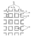
次に、図2〜図5を参照して、撮像素子1の動作について説明する。図2はフォトダイオードに蓄積された電荷を第1の画素電荷として垂直転送CCDに転送する様子を示す図、図3は第1の画素電荷読み出し後にフォトダイオードに蓄積された電荷を第2の画素電荷として水平転送CCDに転送しさらに水平方向に転送するとともに、第1の画素電荷を垂直方向に転送する様子を示す図、図4は第1の画素電荷と第2の画素電荷とを加算する様子を示す図、図5は加算された電荷を同一画素内における垂直転送CCDの電荷保持部に退避する様子を示す図である。
Next, the operation of the
撮像素子1には、被写体からの光線を受けて電荷を発生するフォトダイオード32が、複数、マトリクス状に配列されていて、マトリクス状に配列されたこれらのフォトダイオード32が光電変換部を構成している。
The
さらに、撮像素子1は、光電変換部のフォトダイオード32の各行に隣接して行方向に配置された水平転送レジスタでありぶれ補正部、加算部たる水平転送CCD33を備えている。この水平転送CCD33は、フォトダイオード32で発生した電荷を読み出して得られた第1画像を記憶するとともに、この第1画像を水平方向に転送するものである。
Further, the
また、撮像素子1は、光電変換部のフォトダイオード32の各列に隣接して列方向に配置された垂直転送レジスタでありぶれ補正部、加算部たる垂直転送CCD34を備えている。この垂直転送CCD34は、第1画像よりも前の時刻に得られた電荷を加算した加算電荷に係る第2画像を記憶するとともに、この第2画像を垂直方向に転送するものである。
The
そして、水平転送CCD33と垂直転送CCD34とが交差する位置に配置された電極部分(図6に示す電極φV0,φH0)は、後述するように、第1画像と第2画像とをアナログ加算する加算部として機能するようになっている。
An electrode portion (electrodes φV0 and φH0 shown in FIG. 6) arranged at a position where the
なお、ここでは、複数のフォトダイオード32が、縦方向と、この縦方向に垂直な横方向と、に配列されてマトリクス状をなしている例を示しているが、実質的なマトリクス状をなす配列であればこれに限るものではない。例えば、一方向と、この一方向に斜めに交差する他方向と、に配列されてマトリクス状をなしているものでも構わない。このときには、水平転送CCD33と垂直転送CCD34とを、互いに斜めに交差する方向に配置すれば良い。さらに、フォトダイオード32の形状も正方形や矩形に限るものではなく、平行四辺形や三角形、六角形等の各種の形状であっても構わない。
Here, an example is shown in which a plurality of
そして、撮像素子1における1画素31は、1つのフォトダイオード32と、このフォトダイオード32に隣接する水平転送CCD33の部分および垂直転送CCD34の部分と、を含んでいる。なお、この撮像素子1の転送電極の構造については後述することにする。従って、撮像素子1の1画素に含まれる電極についても後述する。また、1画素31のサイズを、水平方向(横方向)の長さがLx、垂直方向(縦方向)の長さがLyであるとする。
One
このような構成の撮像素子1の作用の概略について説明する。
An outline of the operation of the
以下では、撮像素子1の左上角に配置されたフォトダイオードをP1,1 と表記し、水平方向右側へ向かってi(iは1以上の整数)番目、垂直方向下側へ向かってj(jは1以上の整数)番目の位置に配置されたフォトダイオードをPi,j と表記することにする。
In the following, the photodiode disposed at the upper left corner of the
図2は、最初に光電変換し蓄積されたフォトダイオードPi,j の電荷(第1の画素電荷)(図中において丸印で示している)を、このフォトダイオードPi,j に隣接する垂直転送CCD34にシフトした(読み出した)ところを示している。なお、この図2においては、フォトダイオードPi,j に係る第1の画素電荷のみを図示しているが、他の全てのフォトダイオードにおいて同一の時間だけ光電変換し蓄積された電荷も、同様に垂直転送CCD34に一斉にシフトされることになる。
FIG. 2 shows the vertical transfer of the charge (first pixel charge) of the photodiode Pi, j (photographed by a circle in the figure) first photoelectrically converted and accumulated. A position shifted (read out) to the
図3は、第1の画素電荷をシフトした直後から光電変換し蓄積されたフォトダイオードPi-1,j-1 の電荷(第2の画素電荷)を、このフォトダイオードPi-1,j-1 に隣接する水平転送CCD33にまずシフトした(読み出した)ことを示している。なお、この図3においても、フォトダイオードPi-1,j-1 に係る第2の画素電荷のみを図示しているが、他の全てのフォトダイオードにおいて同一の時間だけ光電変換し蓄積された電荷が、同様に水平転送CCD33に一斉にシフトされることになる。ここに、第1の画素電荷蓄積時にフォトダイオードPi,j に到達していた被写体からの光が、第2の画素電荷蓄積時には手ぶれ等によりフォトダイオードPi-1,j-1 に到達する位置に移っているものとする。この光の到達位置の変化は、第2の画素電荷の蓄積が終わった時点で初めて判明するために、図2に示した状態においては、第1の画素電荷はまだ転送されず、垂直転送CCD34に保持(記憶)されるのみである。しかし、第2の画素電荷を読み出した後は、角速度センサ19,20の出力により光の到達位置の変化が判明するために、同一の被写体光に係る第1の画素電荷と第2の画素電荷との位置関係が分かり、後述する加算を行うために、互いに近接する位置(同一の1画素31内の位置)への転送が行われる。すなわち、図3には、第2の画素電荷が水平転送CCD33上を紙面右方向に1画素分転送されるとともに、第1の画素電荷が垂直転送CCD34上を紙面上方向に1画素分転送される例が示されている。水平転送CCD33による1画素分以上の画素電荷の転送と、垂直転送CCD34による1画素分以上の画素電荷の転送と、は後述する図6に示すような構成では同時に行うことができない(もちろん、同時に行うことができるように構成しても構わない(例えば、水平転送CCD33と垂直転送CCD34とを撮像素子1の厚み方向に異なる位置に独立に設けて、さらに独立に加算部を設けるようにすれば良い。))ために、何れか一方の転送を先に行い、その後に他方の転送を行うことになる。なお、第1の画素電荷の転送と第2の画素電荷の転送とが、全てのフォトダイオードに係る画素電荷について行われるのは上述と同様である。このような水平転送CCD33による転送と垂直転送CCD34による転送とを行うためには、各転送CCDが交差する位置において水平転送CCD33内の電荷と垂直転送CCD34内の電荷とが干渉することのないように、転送電極の配置を工夫する必要があるが、これについては後で説明する。
FIG. 3 shows the charge (second pixel charge) of the photodiode Pi-1, j-1 that has been photoelectrically converted and stored immediately after shifting the first pixel charge, and this photodiode Pi-1, j-1. It is shown that the data is first shifted (read out) to the
図4は、第1の画素電荷と第2の画素電荷とを、水平転送CCD33と垂直転送CCD34とが交差する位置にシフトして、該交差位置において加算した様子(加算であることを、図4中において「+」により示している)を示している。この加算は、全てのフォトダイオードに係る第1の画素電荷と、全てのフォトダイオードに係る第2の加算電荷と、について行われることは勿論である。
FIG. 4 shows a state in which the first pixel charge and the second pixel charge are shifted to a position where the
これにより、第1の画像(全ての第1の画素電荷で構成される画像)と、この第1の画像の直後に連続して撮影された第2の画像(全ての第2の画素電荷で構成される画像)と、がぶれ量だけシフトされた後に、つまりぶれを補正された後に、合成されたことになる。 As a result, the first image (image composed of all the first pixel charges) and the second image (all the second pixel charges captured continuously immediately after the first image). The image is composed after being shifted by the blur amount, that is, after the blur is corrected.
なお、3番目以降の時分割画像を新たに読み出した場合には、第1の画像に相当するのは、それまでの時分割画像を加算して得られた加算画像(最初の時分割画像から最新の1つ前の時分割画像までを順次ぶれ補正して加算して得られた画像)となるために、この図4に示すような動作を行うことにより、新たな時分割画像(全ての新たな画素電荷で構成される画像)と、加算画像と、の相対的なぶれ量が補正された後に、合成されることになる。 When the third and subsequent time-division images are newly read out, the first image corresponds to the addition image obtained by adding the time-division images obtained so far (from the first time-division image). In order to obtain an image obtained by sequentially correcting and adding up to the latest one time-division image, an operation as shown in FIG. An image composed of new pixel charges) and the added image are combined and corrected after being corrected.
図5は、水平転送CCD33と垂直転送CCD34との交差位置において加算された画素電荷を、同一画素内における例えば垂直転送CCD34の電荷保持部に転送した(退避させた)様子を示している。交差位置は、水平転送と垂直転送との両方に用いられるために、該交差位置に加算電荷を保持したままであると、次に読み出した画素電荷との加算を行うことができない。
FIG. 5 shows a state in which the pixel charge added at the intersection of the
そこで、ここでは、加算後の電荷を、一旦、垂直転送CCD34の電荷保持部へ退避させるようにしたものである。これにより、次の画素電荷を水平転送CCD33へ読み出せば、上述と同様に、画素の加算を行うことが可能となる。
Therefore, here, the added charge is temporarily saved in the charge holding unit of the
なお、ここでは、加算後の電荷を同一画素内における垂直転送CCD34の電荷保持部へ転送した(退避させた)が、これに代えて、同一画素内における水平転送CCD33の電荷保持部へ転送しても(退避させても)構わない。このときには、次の画素電荷は、垂直転送CCD34へ読み出されることになる。また、加算後の画素電荷を退避させるのは、必ずしも同一画素内に限るものではない。
Here, the added charge is transferred (retracted) to the charge holding unit of the
従って、図2〜図5に示したような例に限らず、加算電荷は、水平転送CCD33と垂直転送CCD34との何れか一方の記憶部に記憶させれば良く、新たな画素電荷は、水平転送CCD33と垂直転送CCD34との何れか他方の記憶部へ読み出して記憶させれば良い。
Therefore, the added charge is not limited to the examples shown in FIGS. 2 to 5, and the added charge may be stored in one of the storage units of the
以上説明したように、
画像の水平転送CCDへのシフト
→ 相対的なぶれ補正のための電荷転送
→ 電荷の加算
→ 加算した電荷を水平転送CCDと垂直転送CCDとが交差する位置から退避する
というシーケンスを繰り返し行うようになっている。ただし、複数の時分割露光の内の最初の時分割露光による時分割画像については、ぶれ量が0、垂直転送CCDの電荷の加算値が0であるとして、同様のシーケンスを実行すれば足りる。
As explained above,
Shift of image to horizontal transfer CCD → Charge transfer for relative blur correction → Addition of charge → Repeat the sequence of saving the added charge from the position where horizontal transfer CCD and vertical transfer CCD intersect It has become. However, for the time-division image obtained by the first time-division exposure among a plurality of time-division exposures, it is sufficient to execute the same sequence on the assumption that the blur amount is 0 and the charge transfer value of the vertical transfer CCD is 0.
なお、図2〜図5においては、加算画像に対して新たな時分割画像が左方向に1画素かつ上方向に1画素だけずれている例を示したが、一般的には、ずれ量に応じた適宜の画素数だけ水平方向および垂直方向に移動させることになる。これについては、後で図13〜図22等を参照して説明する。 2 to 5 show an example in which a new time-division image is shifted by one pixel in the left direction and by one pixel in the upward direction with respect to the added image. The appropriate number of pixels is moved in the horizontal and vertical directions. This will be described later with reference to FIGS.
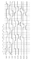
続いて、図6は、固体撮像素子に設けられたフォトダイオードおよび電極の構成を示す図である。 Subsequently, FIG. 6 is a diagram illustrating a configuration of a photodiode and an electrode provided in the solid-state imaging device.
図6に示す各電極は、多結晶シリコンから構成されており、隣接する電極同士は層間絶縁層を介して配置されている。そして、隣接する電極同士は、撮像面に垂直な方向から見たときに、端面同士が一部重なるように配設されている。この図6において、電極の破線で示されている端面は、該電極の端面部分が他方の電極の下部に配置されていることを意味している。 Each electrode shown in FIG. 6 is made of polycrystalline silicon, and adjacent electrodes are arranged via an interlayer insulating layer. The adjacent electrodes are arranged such that the end faces partially overlap each other when viewed from the direction perpendicular to the imaging surface. In FIG. 6, the end face indicated by a broken line of the electrode means that the end face portion of the electrode is disposed below the other electrode.
そして、同一の駆動パルスを印加する電極同士は、コンタクト部を介して所定の配線層により相互に接続されている。ただし、この図6においては、電極の配置を明瞭にするために、電極同士の配線については図示を省略している。 The electrodes to which the same drive pulse is applied are connected to each other by a predetermined wiring layer via a contact portion. However, in FIG. 6, in order to clarify the arrangement of the electrodes, the wiring between the electrodes is not shown.
上述したように、撮像素子1には、複数の(実質的には、多数の)フォトダイオード(図6中、「PD」と記載している)32が、マトリクス状に配列されている。
As described above, the
1つの画素には、1つのフォトダイオード32と、水平転送CCD33を構成する4つの電極、すなわち、左から右へ向かって順にφH1,φH2,φH3,φH0と、垂直転送CCD34を構成する4つの電極、すなわち、上から下へ向かって順にφV0,φV1,φV2,φV3と、が含まれている。
One pixel includes one
なお、φV0〜φV3,φH0〜φH3は、後述するように電荷転送用の駆動パルスを示すものであるが、例えば「転送電極φV0」なる記載は、「駆動パルスφV0を印加する電極」を意味するものとする。 Note that φV0 to φV3 and φH0 to φH3 indicate drive pulses for charge transfer as described later. For example, the description “transfer electrode φV0” means “electrode to which the drive pulse φV0 is applied”. Shall.
上述した各転送電極の内の、垂直転送電極φV2と水平転送電極φH2とはフォトダイオード32の電荷を読み出すための読み出し電極を兼ねたものとなっている。さらに、これらの垂直転送電極φV2と水平転送電極φH2とは、上述した電荷保持部を構成する電極となっている。すなわち、垂直転送電極φV2は、水平転送CCD33を構成する電極φH0,φH1,φH2,φH3の何れとも隣接していないために、φV1およびφV3をVL(例えば、−5[V])にした状態で、φV2をVM(例えば、0[V])にすれば、この垂直転送電極φV2下に加算後の電荷を保持したまま、水平転送CCD33による転送を行うことが可能である(垂直転送電極φV2下の電荷が、水平転送CCD33により転送される電荷と混合することはない)。同様に、水平転送電極φH2は、垂直転送CCD34を構成する電極φV0,φV1,φV2,φV3の何れとも隣接していないために、φH1およびφH3をVLにした状態で、φH2をVMとすれば、この水平転送電極φH2下に加算後の電荷を保持したまま、垂直転送CCD34による転送を行うことが可能である(水平転送電極φH2下の電荷が、垂直転送CCD34により転送される電荷と混合することはない)。このような電荷の混合を避ける機能を果たすために、撮像素子1は、1画素に対して、垂直方向転送用に4つの電極を配置するとともに、水平転送用に4つの電極を配置した構成としている。
Of the transfer electrodes described above, the vertical transfer electrode φV2 and the horizontal transfer electrode φH2 also serve as read electrodes for reading the charge of the
また、垂直転送CCD34と水平転送CCD33とが交差する位置に配置された転送電極は、垂直転送電極φV0と水平転送電極φH0とを兼用したものとなっている。従って、同一の電極ではあるが、用途等に応じて、適宜、垂直転送電極φV0、水平転送電極φH0、あるいは転送電極φV0,φH0などと称することにする。この転送電極φV0,φH0は、電荷の垂直方向または水平方向への転送に用いられるだけでなく、電極φH2と電極φV2との何れか一方の電荷保持部に保持されている電荷と、フォトダイオード32から電極φH2と電極φV2との何れか他方へ新たに読み出された電荷と、を加算するための上記加算部として機能するようになっている。
The transfer electrodes arranged at the positions where the
なお、垂直転送電極φV0,φV1,φV2,φV3を含む垂直転送CCD34を垂直転送レジスタといい、水平転送電極φH0,φH1,φH2,φH3を含む水平転送CCD33を水平転送レジスタという。これら垂直転送レジスタと水平転送レジスタとは、共に、上述したように、電荷を保持(記憶)して転送する機能を備えている。
The
また、本実施形態においては、複数回の撮影による画素の電荷が加算されるために、画素の電荷が転送レジスタの蓄積容量を超えてあふれる可能性がある。以下では、これを防止するための構成について、図7および図8を参照して説明する。図7は撮像素子が縦型オーバーフロー構造であることを説明するための断面図、図8は時分割露光の回数に応じて逆バイアス電圧を変化させオーバーフローが発生する蓄積電荷量を制御する様子を示す図である。 Further, in this embodiment, since the charge of the pixel from a plurality of shootings is added, the charge of the pixel may overflow beyond the storage capacity of the transfer register. Below, the structure for preventing this is demonstrated with reference to FIG. 7 and FIG. FIG. 7 is a cross-sectional view for explaining that the imaging device has a vertical overflow structure, and FIG. 8 shows a state in which the reverse charge voltage is changed according to the number of time-division exposures to control the amount of accumulated charge that causes overflow. FIG.
フォトダイオードに強い光が入射すると、フォトダイオードからあふれた電荷が隣のフォトダイオードに流れ込むことがある。このブルーミング現象を防止するために、従来から、様々な工夫が施されている。本実施形態においては、撮像素子1の内部で電荷を加算するために、例え、m(mは1以上の整数)回の時分割撮影におけるそれぞれの露光量を、通常撮影における露光量の1/mにしたとしても、各時分割画像を加算した画像の電荷は垂直転送CCDの転送容量をはるかに超えてしまう可能性がある。従って、加算した後の画像の電荷が垂直転送CCDの転送能力を超えないようにする必要がある。
When strong light is incident on a photodiode, charges overflowing from the photodiode may flow into the adjacent photodiode. In order to prevent this blooming phenomenon, various devices have been conventionally made. In the present embodiment, in order to add charges inside the
このために、本実施形態においては、縦型オーバーフロー構造のCCD固体撮像素子を採用している。これは、図7に示すように、n型基板(例えば、n型シリコン基板)の表面に作られたp型拡散領域(pウェル:p−well)の中にフォトダイオード(PD)を構成し、pウェルとn型基板との間の逆バイアス電圧VSUBにより、pウェルを完全に空乏化するようにしたものである。 For this reason, in this embodiment, a CCD solid-state imaging device having a vertical overflow structure is employed. As shown in FIG. 7, a photodiode (PD) is formed in a p-type diffusion region (p-well) formed on the surface of an n-type substrate (for example, an n-type silicon substrate). The p well is completely depleted by the reverse bias voltage VSUB between the p well and the n-type substrate.
図8に示すように、フォトダイオード(PD)から垂直転送CCDまたは水平転送CCDに読み出すためのゲートは、垂直転送電極φV2(または水平転送電極φH2)と共通になっている。そして、読み出しゲートの電位φVRGは、転送電極に低電圧(VL)または中電圧(VM)が印加されているときには、フォトダイオードの電位φVPDよりも所定電位だけ低くなっている。これに対して、転送電極に高い電圧(VH)のパルスを印加すると、読み出しゲートの電位φVRGがフォトダイオードの電位φVPDよりも高くなり、フォトダイオード内の信号電荷が垂直転送CCDまたは水平転送CCDへ読み出される。 As shown in FIG. 8, the gate for reading from the photodiode (PD) to the vertical transfer CCD or horizontal transfer CCD is common to the vertical transfer electrode φV2 (or horizontal transfer electrode φH2). The read gate potential φVRG is lower than the photodiode potential φVPD by a predetermined potential when a low voltage (VL) or a medium voltage (VM) is applied to the transfer electrode. In contrast, when a high voltage (VH) pulse is applied to the transfer electrode, the potential φVRG of the readout gate becomes higher than the potential φVPD of the photodiode, and the signal charge in the photodiode is transferred to the vertical transfer CCD or horizontal transfer CCD. Read out.
このとき、垂直転送CCDまたは水平転送CCDは、転送することが可能な最大の電荷量である取扱い電荷量が限られているために、強い光が入射したときに過剰な電荷を排出する動作が必要になる。この過剰な信号電荷は、転送CCD側や他のフォトダイオード側へあふれる前に、縦方向(基板厚み方向)のn+pnの経路を通って基板中に吸収される。すなわち、オーバーフローが行われるpウェルの電位φVOFGは、読み出しゲートを兼ねる転送電極の電圧がVM(0[V])またはVL(−5[V])のときには、読み出しゲート電圧φVRGよりも高くなるように設定されている。これにより、蓄積時に過剰な電荷が垂直転送CCDまたは水平転送CCDに漏れるブルーミングの現象を抑制するようになっている。 At this time, the vertical transfer CCD or the horizontal transfer CCD has a limited handling charge amount, which is the maximum charge amount that can be transferred, and therefore, an operation of discharging excessive charge when strong light is incident. I need it. This excess signal charge is absorbed into the substrate through an n + pn path in the vertical direction (substrate thickness direction) before overflowing to the transfer CCD side or another photodiode side. That is, the potential φVOFG of the p-well where overflow occurs is higher than the read gate voltage φVRG when the voltage of the transfer electrode that also serves as the read gate is VM (0 [V]) or VL (−5 [V]). Is set to This suppresses the phenomenon of blooming in which excessive charges leak to the vertical transfer CCD or horizontal transfer CCD during storage.
さらに、本実施形態においては、上記pウェルとn型基板との間の逆バイアス電圧VSUBを、時分割撮影の回数m(後述する図14のステップS214において選択する)に応じて通常撮影におけるときに比べて高い電圧(図8に示すような逆バイアス電圧VSUB’)に設定する(つまり、VSUB’はmに依存する)ことにより、オーバーフローが行われるpウェルの電位をφVOFG’(>φVOFG)として、通常撮影のときにフォトダイオードに蓄積される最大電荷量の1/mを超える過剰電荷を基板側に排出するようにしている。このようにすることにより、m回の時分割撮影による画像を加算しても、加算後の総電荷量を垂直転送CCDまたは水平転送CCDの取扱い電荷量以内に抑えることができる。 Further, in the present embodiment, the reverse bias voltage VSUB between the p-well and the n-type substrate is set in the normal photographing according to the number m of time-division photographing (selected in step S214 in FIG. 14 described later). Is set to a higher voltage (reverse bias voltage VSUB ′ as shown in FIG. 8) (that is, VSUB ′ depends on m), so that the potential of the p-well where overflow occurs is φVOFG ′ (> φVOFG) As described above, excess charges exceeding 1 / m of the maximum charge accumulated in the photodiode during normal photographing are discharged to the substrate side. In this way, even if images obtained by m time-division photographing are added, the total charge amount after the addition can be suppressed within the charge amount handled by the vertical transfer CCD or the horizontal transfer CCD.
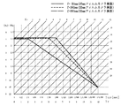
図9は、基板電圧VSUBにより変化するフォトダイオード32の蓄積電荷量の最大値Q(max)を時分割撮影の回数mに応じて設定する様子の幾つかの例を示す線図である。この図9においては、横軸に基板電圧VSUBを、縦軸にフォトダイオード32の蓄積電荷量の最大値Q(max)を、それぞれとっている。
FIG. 9 is a diagram showing several examples of how the maximum value Q (max) of the accumulated charge amount of the
本実施形態では、時分割撮影の回数mとして、m=1〜10の10通りの値を設定することが可能となっていて(図9には、m=1,2,4,8の例を示している。このときには、VSUBは、図示のようなV1,V2,V4,V8の各値となる。)、この時分割撮影の回数として選択可能なmが、例えばEEPROM24に予め記憶されている。フォトダイオード32の蓄積電荷量の最大値Q(max)は、m=1のときを1とすると、mが2〜10の値をとるときには各mに対して1/mとなる(なお、mが11以上の値を取り得るように設定したときにも、Q(max)が1/mとなる規則はそのまま適用可能である。)。また、m=1は通常の撮影(時分割撮影によらない撮影)の場合のフォトダイオード32の蓄積電荷量の最大値に対応する。
In the present embodiment, 10 values of m = 1 to 10 can be set as the number m of time-division shooting (in FIG. 9, examples of m = 1, 2, 4, 8). In this case, VSUB is V1, V2, V4, and V8 as shown in the figure.) M that can be selected as the number of times of time-division shooting is stored in advance in, for example, the
なお、mの最大値を10にしたのは、あまり大きな値にすると、画像データのS/Nを高い値に保持するのが困難になるためである。 The reason why the maximum value of m is set to 10 is that if the value is too large, it is difficult to maintain the S / N of the image data at a high value.
また、本実施形態の技術は、ぶれ限界露光時間TLimit (ここに、ぶれ限界露光時間TLimit は、後で詳しく説明するように、ぶれの発生を実質的に無視し得る程度以下となるような露光時間である。)でm回の時分割撮影を行って画像を加算するものである。従って、ぶれを抑制し得る最長の露光時間をTExp0とすると、本実施形態においては、TExp0は、m(max)・TLimit となる。ここに、m(max)は、mの最大値であって、本実施形態においては上述したようにm(max)=10となる。具体的には、35mmフィルムカメラに換算した撮影レンズの焦点距離が300mmである場合には、ぶれ限界露光時間TLimit は約1/300秒のシャッタスピードとなり、ぶれ補正可能な最長露光時間TExp0は、およそ1/30秒となる。 In addition, the technique of the present embodiment uses the blur limit exposure time TLimit (where the blur limit exposure time TLimit is less than the extent that the occurrence of blur can be substantially ignored, as will be described in detail later). Time), and the image is added m times of time-division shooting. Accordingly, when the longest exposure time that can suppress blur is TExp0, in this embodiment, TExp0 is m (max) · TLimit. Here, m (max) is the maximum value of m, and in this embodiment, m (max) = 10 as described above. Specifically, when the focal length of the photographic lens converted to a 35 mm film camera is 300 mm, the blur limit exposure time TLimit is about 1/300 second shutter speed, and the longest exposure time TExp0 capable of blur correction is Approximately 1/30 second.
こうして、mの値が大きいほど、より長い時間露光に対してぶれ補正を行うことが可能となるが、上述したように、mの値をあまり大きくすると画像データのS/Nが低くなる可能性がある。従って、mの値は、制御の安定性と、時分割撮影による画像のS/Nと、等のバランスを考慮して決めることが望ましい。このような理由から、本実施形態においてはmの最大値を10に設定しているが、これに限る必要はない。 Thus, as the value of m is larger, it is possible to perform blur correction for a longer time exposure. However, as described above, if the value of m is too large, the S / N of the image data may be lowered. There is. Therefore, the value of m is preferably determined in consideration of the balance between the stability of control and the S / N of the image obtained by time-division shooting. For this reason, the maximum value of m is set to 10 in the present embodiment, but this need not be limited.
図10は、撮像時における固体撮像素子1の基本的な動作を示すタイミングチャートである。
FIG. 10 is a timing chart showing the basic operation of the solid-
この図10において、VSUBは、フォトダイオード32に蓄積された電荷を半導体基板(サブストレート)へ強制排出するための基板印加高電圧パルスである。また、φV0〜φV3は4相の垂直転送パルス、φH0〜φH3は4相の水平転送パルスである。
In FIG. 10, VSUB is a high voltage pulse applied to the substrate for forcibly discharging the charge accumulated in the
撮影動作を開始すると、所定のタイミングとなる時刻t01から露光(電荷蓄積)開始時刻t02までの間、VSUBに高電圧のパルスを印加すると同時に、φV0〜φV3に高周波の垂直転送パルスを、φH0〜φH3に高周波の水平転送パルスを、それぞれ印加する。すると、フォトダイオード32に蓄積されている電荷と、水平転送CCD33に残っている電荷と、垂直転送CCD34に残っている電荷と、が全て排出される。
When the photographing operation is started, a high-voltage pulse is applied to VSUB from time t01 at a predetermined timing to exposure (charge accumulation) start time t02, and at the same time, a high-frequency vertical transfer pulse is applied to φV0 to φV3 and φH0 to φH0. A high-frequency horizontal transfer pulse is applied to φH3. Then, all the charges accumulated in the
その後、露光動作開始の信号を受けると、時刻t02のタイミングにおいてVSUBへの高電圧パルスの印加を停止することにより、受けた光の強度に応じた電荷がフォトダイオード32に蓄積される。このフォトダイオード32への電荷の蓄積は、時刻t02から時刻t03までの露光時間TExp において継続的に行われる。そして、この露光時間TExp をぶれが発生しないような時間間隔に時分割して、各時分割画像をぶれに応じて繰り返し転送し加算することにより、ぶれ補正が行われた露光時間TExp の1枚の画像データを得るようになっている。この露光時間TExp における撮像素子1の動作については、後でより詳しく説明する。
Thereafter, when an exposure operation start signal is received, the application of the high voltage pulse to VSUB is stopped at the timing of time t02, whereby charges corresponding to the intensity of the received light are accumulated in the
時刻t03において露光が終了すると、垂直転送CCD34に蓄積されているぶれの補正された画像が、上記垂直転送CCD34と、撮像領域から外部へ出力するための読出部および転送部たる水平転送CCD42(図12参照)と、を介して、通常の読み出し速度で撮像素子1から読み出される。
When the exposure is completed at time t03, the blur-corrected image accumulated in the
図11は、フォトダイオードから画素電荷を読み出して固体撮像素子内で転送し加算するときに各電極に印加される信号の様子を示すタイミングチャートである。なお、ここでは、図6に示すような構成の撮像素子1により、図2〜図5を参照して説明したような動作を行うときの例について示している。また、電極φV0と電極φH0とは共通であるために、この図11においてはまとめて記載している。
FIG. 11 is a timing chart showing a state of signals applied to the respective electrodes when pixel charges are read from the photodiodes, transferred in the solid-state imaging device, and added. Here, an example in which the operation described with reference to FIGS. 2 to 5 is performed by the
今、時刻t1までに、垂直転送CCD34の電荷保持部(電極φV2下)には既に加算された電荷が記憶されているものとし、かつ、時刻t1において最新の時分割露光が終了したものとする。ただし、時刻t1が複数の時分割露光の内の最初の時分割露光が終了した時点であるときは、上述したように、垂直転送CCD中34で加算され記憶されている電荷が0であるとすれば、一般化することができる。
Now, it is assumed that the added charge has already been stored in the charge holding portion (below the electrode φV2) of the
時刻t1に所定の露光時間が経過したら、電極φH2に読み出し用の高電圧(トランスファーパルス)VH(15[V])を印加する。このときには、加算電荷を保持する電極φV2が中電圧VM(0[V])で、それ以外の電極φV0,φV1,φV3,φH1,φH3は、全て低電圧VL(−5[V])に設定されている。これにより、フォトダイオード32に蓄積された電荷が、水平転送CCD33の電極φH2下にシフトされる。シフトが行われたら、電極φH2への印加電圧は中電圧VM(0[V])になり、読み出された電荷がこの電極φH2下において保持(蓄積)される(図3参照)。
When a predetermined exposure time elapses at time t1, a high voltage (transfer pulse) VH (15 [V]) for reading is applied to the electrode φH2. At this time, the electrode φV2 holding the added charge is set to the medium voltage VM (0 [V]), and the other electrodes φV0, φV1, φV3, φH1, and φH3 are all set to the low voltage VL (−5 [V]). Has been. As a result, the charge accumulated in the
電極φH2に印加される電圧が高電圧VH(15[V])から中電圧VM(0[V])に変化すると同時に、フォトダイオード32では次の撮影のための電荷の蓄積が開始される。すなわち、次の時分割撮影の開始である。
At the same time as the voltage applied to the electrode φH2 changes from the high voltage VH (15 [V]) to the medium voltage VM (0 [V]), the
その後、時刻t2を過ぎたタイミングで、電極φH3に中電圧VMが印加される。これにより、電極φH2下において保持されていた電荷が、一部、電極φH3下へ転送され、電極φH2および電極φH3の両方の電極下のポテンシャル井戸(以下、単に「電極下」という。)に保持される。 Thereafter, the intermediate voltage VM is applied to the electrode φH3 at a timing after the time t2. As a result, the charge held under the electrode φH2 is partially transferred under the electrode φH3 and held in a potential well (hereinafter simply referred to as “under the electrode”) under both the electrodes φH2 and φH3. Is done.
次に、時刻t3を過ぎたタイミングで、電極φH2が低電圧VLに設定される。これにより、電極φH2および電極φH3の両方の電極下に保持されていた電荷は、全部、電極φH3下へ転送され、この電極φH3下に保持される。 Next, at the timing after time t3, the electrode φH2 is set to the low voltage VL. As a result, the charges held under both electrodes φH2 and φH3 are all transferred under electrode φH3 and held under electrode φH3.
電極φH2が低電圧VLに設定された直後に、電極φH0(電極φV0)が中電圧VMに設定される。これにより、電極φH3下に保持されていた電荷が、一部、電極φH0下へ転送され、電極φH3および電極φH0の両方の電極下に保持される。 Immediately after the electrode φH2 is set to the low voltage VL, the electrode φH0 (electrode φV0) is set to the medium voltage VM. Thereby, a part of the electric charge held under the electrode φH3 is transferred under the electrode φH0 and held under both the electrodes φH3 and φH0.
その後、時刻t4を過ぎたタイミングで、電極φH3が低電圧VLに設定される。これにより、電極φH3および電極φH0の両方の電極下に保持されていた電荷は、全部、電極φH0下へ転送され、この電極φH0下に保持される。 Thereafter, at a timing after time t4, the electrode φH3 is set to the low voltage VL. As a result, all the charges held under both electrodes φH3 and φH0 are transferred under electrode φH0 and held under electrode φH0.
電極φH3が低電圧VLに設定された直後に、電極φH1が中電圧VMに設定される。これにより、電極φH0下に保持されていた電荷が、一部、隣接する画素の電極φH1下へ転送され、電極φH0および電極φH1の両方の電極下に保持される。 Immediately after the electrode φH3 is set to the low voltage VL, the electrode φH1 is set to the medium voltage VM. As a result, a part of the electric charge held under the electrode φH0 is transferred under the electrode φH1 of the adjacent pixel, and is held under both the electrodes φH0 and φH1.
時刻t5を過ぎたタイミングで、電極φH0が低電圧VLに設定される。これにより、電極φH0および電極φH1の両方の電極下に保持されていた電荷は、全部、電極φH1下へ転送され、この電極φH1下に保持される。 At the timing after time t5, the electrode φH0 is set to the low voltage VL. As a result, all the charges held under both electrodes φH0 and φH1 are transferred under electrode φH1 and held under electrode φH1.
電極φH0が低電圧VLに設定された直後に、電極φH2が中電圧VMに設定される。これにより、電極φH1下に保持されていた電荷が、一部、電極φH2下へ転送され、電極φH1および電極φH2の両方の電極下に保持される。 Immediately after the electrode φH0 is set to the low voltage VL, the electrode φH2 is set to the medium voltage VM. As a result, a part of the electric charge held under the electrode φH1 is transferred under the electrode φH2 and held under both the electrodes φH1 and φH2.
その後、時刻t6を過ぎたタイミングで、電極φH1が低電圧VLに設定される。これにより、電極φH1および電極φH2の両方の電極下に保持されていた電荷は、全部、電極φH2下へ転送され、この電極φH2下に保持される。 Thereafter, at a timing after time t6, the electrode φH1 is set to the low voltage VL. As a result, all the charges held under both electrodes φH1 and φH2 are transferred under electrode φH2 and held under electrode φH2.
このようにして、水平転送CCD33のある画素の電極φH2下に保持されていた電荷が、右に隣接する画素の電極φH2下まで、
電極φH2下 → 電極φH3下 → 電極φH0下 → 電極φH1下 → 電極φH2下
のように転送される。
In this way, the charge held under the electrode φH2 of the pixel with the
The transfer is performed in the following order: under
この隣接する画素の電極φH2下の電荷は、時刻t11を過ぎるタイミングまで引き続き該電極φH2下に保持(記憶)される(図3参照)。 The charge under the electrode φH2 of the adjacent pixel is continuously held (stored) under the electrode φH2 until the timing after the time t11 (see FIG. 3).
なお、ここでは、水平転送CCD33により電荷を1画素分右方向に転送するとき(図3参照)の動作について説明したが、より一般に、n(nは1以上の整数)画素分の転送を行うときには、上述したようなφH0〜φH3の信号をn回繰り返して与えれば良い。また、水平転送CCD33により電荷を左方向に転送することも可能である。このときには、上述とは時間反転させた信号を、各電極φH0〜φH3に与えれば良い。そして、左方向にn画素分の転送を行うときには、この時間反転させた信号をn回繰り返して各電極φH0〜φH3に与えることになる。
Here, the operation when the charge is transferred rightward by one pixel by the horizontal transfer CCD 33 (see FIG. 3) has been described, but transfer of n (n is an integer of 1 or more) pixels is more generally performed. In some cases, the signals of φH0 to φH3 as described above may be repeated n times. It is also possible to transfer charges in the left direction by the
続いて、時刻t7を過ぎたタイミングで、電極φV1が中電圧VMに設定される。これにより、電極φV2下に保持されていた加算電荷が、一部、電極φV1下へ転送され、電極φV2および電極φV1の両方の電極下に保持される。 Subsequently, at the timing after time t7, the electrode φV1 is set to the medium voltage VM. Thereby, a part of the added charge held under the electrode φV2 is transferred under the electrode φV1 and held under both the electrodes φV2 and φV1.
その後、時刻t8を過ぎたタイミングで、電極φV2が低電圧VLに設定される。これにより、電極φV2および電極φV1の両方の電極下に保持されていた電荷は、全部、電極φV1下へ転送され、この電極φV1下に保持される。 Thereafter, at the timing after time t8, the electrode φV2 is set to the low voltage VL. As a result, all the charges held under both electrodes φV2 and φV1 are transferred under electrode φV1 and held under electrode φV1.
電極φV2が低電圧VLに設定された直後に、電極φV0(電極φH0)が中電圧VMに設定される。これにより、電極φV1下に保持されていた電荷が、一部、電極φV0下へ転送され、電極φV1および電極φV0の両方の電極下に保持される。 Immediately after the electrode φV2 is set to the low voltage VL, the electrode φV0 (electrode φH0) is set to the medium voltage VM. Thereby, a part of the electric charge held under electrode φV1 is transferred under electrode φV0 and held under both electrodes φV1 and φV0.
次に、時刻t9を過ぎたタイミングで、電極φV1が低電圧VLに設定される。これにより、電極φV1および電極φV0の両方の電極下に保持されていた電荷は、全部、電極φV0下へ転送され、この電極φV0下に保持される。 Next, at the timing after time t9, the electrode φV1 is set to the low voltage VL. As a result, all of the charges held under both electrodes φV1 and φV0 are transferred under electrode φV0 and held under electrode φV0.
電極φV1が低電圧VLに設定された直後に、電極φV3が中電圧VMに設定される。これにより、電極φV0下に保持されていた電荷が、一部、電極φV3下へ転送され、電極φV0および電極φV3の両方の電極下に保持される。 Immediately after the electrode φV1 is set to the low voltage VL, the electrode φV3 is set to the medium voltage VM. Thereby, a part of the electric charge held under electrode φV0 is transferred under electrode φV3 and held under both electrodes φV0 and φV3.
時刻t10を過ぎたタイミングで、電極φV0が低電圧VLに設定される。これにより、電極φV0および電極φV3の両方の電極下に保持されていた電荷は、全部、電極φV3下へ転送され、この電極φV3下に保持される。 At the timing after time t10, the electrode φV0 is set to the low voltage VL. As a result, all the charges held under both electrodes φV0 and φV3 are transferred under electrode φV3 and held under electrode φV3.
電極φV0が低電圧VLに設定された直後に、電極φV2が中電圧VMに設定される。これにより、電極φV3下に保持されていた電荷が、一部、電極φV2下へ転送され、電極φV3および電極φV2の両方の電極下に保持される。 Immediately after the electrode φV0 is set to the low voltage VL, the electrode φV2 is set to the medium voltage VM. Thereby, a part of the electric charge held under the electrode φV3 is transferred to the lower side of the electrode φV2 and is held under both the electrodes φV3 and φV2.
その後、時刻t11を過ぎたタイミングで、電極φV3が低電圧VLに設定される。これにより、電極φV3および電極φV2の両方の電極下に保持されていた電荷は、全部、電極φV2下へ転送され、この電極φV2下に保持される。 Thereafter, at the timing after time t11, the electrode φV3 is set to the low voltage VL. As a result, all the charges held under both electrodes φV3 and φV2 are transferred under electrode φV2 and held under electrode φV2.
このようにして、垂直転送CCD34のある画素の電極φV2下に保持されていた電荷が、上に隣接する画素の電極φV2下まで、
電極φV2下 → 電極φV1下 → 電極φV0下 → 電極φV3下 → 電極φV2下
のように転送される。
In this way, the electric charge held under the electrode φV2 of the pixel having the
It is transferred in the following order: under
なお、ここでは、垂直転送CCD34により電荷を1画素分上方向に転送するとき(図3参照)の動作について説明したが、より一般に、n(nは1以上の整数)画素分の転送を行うときには、上述したようなφV0〜φV3の信号をn回繰り返して与えれば良い。また、垂直転送CCD34により電荷を下方向に転送することも可能である。このときには、上述とは時間反転させた信号を、各電極φV0〜φV3に与えれば良い。そして、下方向にn画素分の転送を行うときには、この時間反転させた信号をn回繰り返して各電極φV0〜φV3に与えることになる。
Here, the operation when the charge is transferred upward by one pixel by the vertical transfer CCD 34 (see FIG. 3) has been described, but more generally transfer of n (n is an integer of 1 or more) pixels is performed. In some cases, the above-described signals of φV0 to φV3 may be repeated n times. It is also possible to transfer charges downward by the
時刻t11を過ぎたタイミングにおいて、電極φV3が低電圧VLに設定された直後に、電極φV1が中電圧VMに設定される。これにより、電極φV2下に保持されていた電荷が、一部、電極φV1下へ転送され、電極φV2および電極φV1の両方の電極下に保持される。 At a timing after time t11, immediately after the electrode φV3 is set to the low voltage VL, the electrode φV1 is set to the medium voltage VM. As a result, a part of the electric charge held under the electrode φV2 is transferred under the electrode φV1 and held under both the electrodes φV2 and φV1.
これと同時に、電極φH3が中電圧VMに設定される。これにより、電極φH2下に保持されていた電荷が、一部、電極φH3下へ転送され、電極φH2および電極φH3の両方の電極下に保持される。 At the same time, the electrode φH3 is set to the medium voltage VM. Thereby, a part of the electric charge held under the electrode φH2 is transferred under the electrode φH3 and held under both the electrodes φH2 and φH3.
時刻t12を過ぎたタイミングにおいて、電極φV2が低電圧VLに設定される。これにより、電極φV2および電極φV1の両方の電極下に保持されていた電荷は、全部、電極φV1下へ転送され、この電極φV1下に保持される。 At the timing after time t12, the electrode φV2 is set to the low voltage VL. As a result, all the charges held under both electrodes φV2 and φV1 are transferred under electrode φV1 and held under electrode φV1.
これと同時に、電極φH2が低電圧VLに設定される。これにより、電極φH2および電極φH3の両方の電極下に保持されていた電荷は、全部、電極φH3下へ転送され、この電極φH3下に保持される。 At the same time, the electrode φH2 is set to the low voltage VL. As a result, the charges held under both electrodes φH2 and φH3 are all transferred under electrode φH3 and held under electrode φH3.
電極φV2が低電圧VLに設定され、かつ電極φH2が低電圧VLに設定された直後に、電極φV0,φH0が中電圧VMに設定される。これにより、電極φV1下に保持されていた電荷が、一部、電極φV0,φH0下および電極φH3下へ転送されるとともに、電極φH3下に保持されていた電荷が、一部、電極φV0,φH0下および電極φV1下へ転送される。従って、この時点で、電荷の混合(加算)が生じることになる(図4参照)。 Immediately after the electrode φV2 is set to the low voltage VL and the electrode φH2 is set to the low voltage VL, the electrodes φV0 and φH0 are set to the medium voltage VM. Thereby, a part of the electric charge held under the electrode φV1 is transferred to the electrodes φV0, φH0 and the electrode φH3, and a part of the electric charge held under the electrode φH3 is partially transferred to the electrodes φV0, φH0. Is transferred down and below the electrode φV1. Therefore, at this time, charge mixing (addition) occurs (see FIG. 4).
その後、時刻t13を過ぎたタイミングにおいて、電極φH3が低電圧VLに設定される。これにより、電極φH3、電極φV0,φH0、および電極φV1の各電極下に保持されていた電荷は、電極φV0,φH0および電極φV1の両電極下にのみ保持される。 Thereafter, at a timing after time t13, the electrode φH3 is set to the low voltage VL. As a result, the charges held under the electrodes φH3, φV0, φH0, and electrode φV1 are held only under the electrodes φV0, φH0, and electrode φV1.
続いて、時刻t14を過ぎたタイミングにおいて、電極φV0,φH0が低電圧VLに設定される。これにより、電極φV0,φH0および電極φV1の両方の電極下に保持されていた電荷が、全部、電極φV1下へ転送され、この電極φV1下に保持される。 Subsequently, at the timing after time t14, the electrodes φV0 and φH0 are set to the low voltage VL. As a result, the charges held under both of the electrodes φV0, φH0 and electrode φV1 are all transferred below electrode φV1 and held under electrode φV1.
電極φV0,φH0が低電圧VLに設定された直後に、電極φV2が中電圧VMに設定される。これにより、電極φV1下に保持されていた電荷が、一部、電極φV2下へ転送され、電極φV1および電極φV2の両方の電極下に保持される。 Immediately after the electrodes φV0 and φH0 are set to the low voltage VL, the electrode φV2 is set to the medium voltage VM. As a result, a part of the electric charge held under the electrode φV1 is transferred to the lower side of the electrode φV2 and held under both the electrodes φV1 and φV2.
時刻t15を過ぎたタイミングにおいて、電極φV1が低電圧に設定される。これにより、電極φV1および電極φV2の両方の電極下に保持されていた電荷が、全部、電極φV2下へ転送され、この電極φV2下に保持される(図5参照)。この状態は、時刻t16においても継続しており、加算電荷が電極φV2下に保持されていることが分かる。 At the timing after time t15, the electrode φV1 is set to a low voltage. As a result, all the charges held under both electrodes φV1 and φV2 are transferred under electrode φV2 and held under electrode φV2 (see FIG. 5). This state continues even at time t16, and it can be seen that the added charge is held under the electrode φV2.
このように上記時刻t12を過ぎたタイミングで加算された電荷を、同一画素内の電極φV2下に転送して記憶することにより、この記憶した画像と次回の時分割露光による画像との加算を、同様のシーケンスで行うことができる。こうして、複数回の撮影による画像のぶれを補正しながら加算して、最終的にぶれのない(「ぶれのない」とは、ぶれが実質的に無視し得る程度以下であることを意味している。)露光時間TExp の画像を得ることができる。 In this way, by adding and storing the charges added at the timing after the time t12 under the electrode φV2 in the same pixel, the addition of the stored image and the image by the next time-division exposure is performed. A similar sequence can be performed. In this way, the image blur caused by multiple shooting is corrected and added, and finally there is no blur (“no blur” means that the blur is substantially less than negligible. An image with an exposure time TExp can be obtained.
上述したように、水平転送CCD33に記憶された画像は、水平方向のぶれ量だけ転送されることにより、水平方向の相対的なぶれが補正される。また、垂直転送CCD34に記憶された画像は、垂直方向のぶれ量だけ転送されることにより、垂直方向の相対的なぶれが補正される。このために、水平転送CCD33および垂直転送CCD34の各々の電極下のポテンシャル井戸には、多数回に渡り隣接するポテンシャル井戸から電荷が転送されて来る。従って、水平転送CCD33の両端および垂直転送CCD34の両端に転送されてくる電荷は、行き場を失ってここに蓄積されてしまう。蓄積された電荷は、やがてポテンシャル井戸に蓄積可能なレベルを越えてしまい、隣接するポテンシャル井戸に流れ込んで、画像の劣化を招くことになる。このような課題を解決する一つの手段として、水平転送CCD33の両端および垂直転送CCD34の両端の電極下のポテンシャル井戸の容量を、電荷が飽和することのないような大きな容量にすることが考えられる。しかし、累積される電荷の量は、被写体の輝度やぶれ量に応じて異なるために、全てのケースにおいて電荷が飽和しないようにするためには、相当に大きな容量のポテンシャル井戸を必要とする。
As described above, the image stored in the
そこで、本実施形態においては、図32に示すように、水平転送CCD33の端部および垂直転送CCD34の端部の転送電極71に隣接してn+拡散領域のドレイン72を設け、転送電極71下のポテンシャル井戸に転送された電荷をドレイン72を介して排出するようにしている。ここに、図32は、水平転送CCD33の端部および垂直転送CCD34の端部に転送された電荷をドレイン72に排出するようにした構成を示す図である。
Therefore, in the present embodiment, as shown in FIG. 32, the
なお、垂直転送CCD34の両端の転送電極の内、水平転送CCD42(図12参照)に面した側については、同様の排出機構を設けることができない。そこで、この水平転送CCD42に面した側については、ぶれ補正を行う間、水平転送CCD42を駆動することにより、垂直転送CCD34から送られて来る電荷を水平転送CCD42の出力部へ排出するようにしている。
A similar discharge mechanism cannot be provided on the side facing the horizontal transfer CCD 42 (see FIG. 12) among the transfer electrodes at both ends of the
図12は、固体撮像素子全体の構成を模式化して示す図である。なお、実用的な固体撮像素子1は例えば数十万〜数百万画素以上の画素数を備えているが、全部を図示することは不可能であるために、この図12においては、これよりも画素数を少なくする模式化を行っている。
FIG. 12 is a diagram schematically showing the configuration of the entire solid-state imaging device. The practical solid-
撮像領域41は、図2〜図5、あるいは図6に示したような、フォトダイオード32と、水平転送CCD33と、垂直転送CCD34と、を含む、撮像部、光電変換部である。
The
上記撮像領域41の上記垂直転送CCD34が突き当たる水平方向位置には、水平転送CCD42が配設されている。この水平転送CCD42は、撮像領域41の垂直転送CCD34において加算された画像を、図10の時刻t03から時刻t04の間に、通常のCCD撮像素子(つまり、例えば、上述したような水平転送CCD33を備えていないCCD撮像素子)と同様に、外部へ読み出すためのものである。なお、この水平転送CCD42には、上述した水平転送CCD33とは異なる水平転送パルスφH4,φH5が印加され、画素電荷の転送を行うようになっている。
A
上記水平転送CCD42の出力側には、該水平転送CCD42から転送されたアナログ信号を増幅するためのアンプ43が配設されている。こうして、撮像素子1からは、アンプ43により増幅された信号が出力されるようになっている。
An
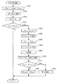
次に、図13は、デジタルカメラにより画像を撮像して記録するときの処理を示すフローチャートである。 Next, FIG. 13 is a flowchart showing processing when an image is captured and recorded by a digital camera.
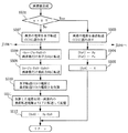
デジタルカメラの電源が投入される(例えば、電池が交換されるなど)か、または、図示しない動作開始スイッチ(例えば、電源スイッチ)が操作されると、このデジタルカメラの動作がスタートする。 When the power of the digital camera is turned on (for example, the battery is replaced) or an operation start switch (not shown) (for example, a power switch) is operated, the operation of the digital camera starts.
処理を開始すると、所定の初期値設定等を行った後に、まず、撮影者のレリーズ操作によって第1レリーズスイッチ18aが閉じた状態になったか否かを判定する(ステップS101)。
When the process is started, after setting a predetermined initial value and the like, first, it is determined whether or not the
ここで、第1レリーズスイッチ18aが閉じていない場合には、J101に分岐して、第1レリーズスイッチ18aの検出を同様に繰り返して行う。ただし、実際には、J101とステップS101との間に、表示を行ったり、その他の図示しないキー入力の状態を検出したりする動作等を行うが、こうした一般的な動作については以下においても適宜説明を省略することにする。
If the
ステップS101において第1レリーズスイッチ18aが閉じたことが検出された場合には、次に、ぶれ限界露光時間TLimit を演算する(ステップS102)。このぶれ限界露光時間TLimit は、露光開始からのぶれ量が許容限界のぶれ量に達すると想定される時間である。
If it is detected in step S101 that the
ここで、ぶれ限界露光時間TLimit について説明する。35ミリフィルムカメラにおける縦24mm×横36mm(対角 43.28mm)のいわゆるライカ版フレーム(別称:ダブルフレーム)カメラに関する長年の経験則として、ミリメートル単位の撮影レンズの焦点距離をfとしたときに、ぶれ限界露光時間TLimit が、TLimit ≒1/f(秒)になるということが知られている。本実施形態においては、この経験則を、デジタルカメラの撮像素子の有効撮像エリア内に設定した撮影画枠の大きさを考慮の上、応用することにする。以下の説明においては、単位mmについての記載を適宜省略して、数値のみを表記することにする。 Here, the blur limit exposure time TLimit will be described. As a long-standing empirical rule for a so-called Leica frame (also known as double frame) camera with a length of 24 mm and a width of 36 mm (diagonal 43.28 mm) in a 35 mm film camera, when the focal length of the taking lens in millimeters is f It is known that the blur limit exposure time TLimit becomes TLimit≈1 / f (seconds). In the present embodiment, this rule of thumb is applied in consideration of the size of the photographic image frame set in the effective imaging area of the imaging device of the digital camera. In the following description, description about the unit mm is omitted as appropriate, and only numerical values are described.
デジタルカメラにおける被写体撮像範囲(撮影画角)は、撮影レンズの焦点距離に反比例し、かつフレームの大きさに比例するために、フレームに対する相対的な像倍率は、焦点距離に比例し、かつフレームの大きさに反比例する。従って、(フレームに対する相対的な)像ぶれもフレームの大きさに反比例する。そこで、上記経験則に対してフレームの大きさ比率に応じた換算係数を乗じて、これを適用すれば良いことになる。この場合、アスペクト比の違いを考慮する必要があるが、本実施形態に係るデジタルカメラにおいては、対角線換算を用いることにする。 Since the subject imaging range (shooting angle of view) in a digital camera is inversely proportional to the focal length of the taking lens and proportional to the size of the frame, the relative image magnification relative to the frame is proportional to the focal length and the frame. Is inversely proportional to the size of Therefore, image blur (relative to the frame) is also inversely proportional to the frame size. Therefore, it is only necessary to multiply the empirical rule by a conversion factor corresponding to the frame size ratio and apply this. In this case, it is necessary to consider the difference in aspect ratio, but in the digital camera according to the present embodiment, diagonal conversion is used.
撮影画枠の対角長をd[mm]とすると、TLimit は次の数式1により表される。
[数1]

[Equation 1]
なお、この数式1の分母(43.28×f/d)は、デジタルカメラの撮影レンズの焦点距離fを、同一画角のライカ版フレームのフィルムカメラの撮影レンズの焦点距離に換算した値になっている。
The denominator (43.28 × f / d) of
この数式1からも明らかなように、このぶれ限界露光時間TLimit は、デジタルカメラの撮影レンズ15が単焦点距離の撮影レンズである場合は該焦点距離に応じた1つの値のみを適用すれば良いが、撮影レンズ15がズームレンズである場合には、焦点距離に応じた異なる値を適用する必要がある。
As is apparent from the
なお、ぶれ限界露光時間TLimit は、必ずしも、数式1で与えられる値を用いる必要はなく、要するに、ぶれが実質的に発生することのないような露光時間を用いれば良い。従って、ぶれ限界露光時間TLimit は、概略、数式1により与えられる露光時間よりも短い時間であれば構わない。
Note that the blur limit exposure time TLimit does not necessarily need to use the value given by
次に、被写体の明るさを測光する(ステップS103)。この測光は、撮像素子1から繰り返し出力される画像信号のレベルをモニタして、被写体の明るさを演算するものである。すなわち、撮像素子1から読み出された画像信号は、CDS2により処理されゲインコントロールアンプ3により増幅された後にA/D変換器4によりデジタル値に変換され、情報処理部8を経てDRAM9に一時的に記憶される。このDRAM9に記憶された画像信号の内、画像全体の中の例えば中央部付近の所定領域の画像信号がCPU7により読み出されて、そのレベルの加算平均値が求められる。そして、CPU7は、求めた加算平均値に基づいて被写体の明るさ(Bv)を計算する。
Next, the brightness of the subject is measured (step S103). In this photometry, the level of an image signal repeatedly output from the
続いて、CPU7は、適正露光を得るために必要なシャッタ速度値(露光時間)TExp や絞り17の絞り値を計算するとともに、計算結果に基づき絞り駆動系16を介して絞り17の絞り設定を行うためのサブルーチン(図14参照)を実行する(ステップS104)。
Subsequently, the
ここに、図14は、TExp と絞り値の演算と絞り設定のサブルーチンを示すフローチャートである。 FIG. 14 is a flowchart showing a subroutine for calculating TExp and the aperture value and setting the aperture.
この図14に示すサブルーチンは、デジタルカメラが制御不能な露出値の場合には警告表示を行い、撮影モードが、シャッタ優先撮影モード、絞り優先撮影モード、プログラム撮影モードの何れに設定されていても、手ぶれ防止を行うようにしたものとなっている。さらに、このサブルーチンは、仮に露光時間が手ぶれが発生する可能性がある露光時間(の閾値)よりも長いときには、予め警告表示をして、手ぶれ防止を優先する撮影モードに自動的に設定し、撮影を行うようにしたものとなっている。 The subroutine shown in FIG. 14 displays a warning when the exposure value is uncontrollable by the digital camera, and the shooting mode is set to any one of the shutter priority shooting mode, the aperture priority shooting mode, and the program shooting mode. It is designed to prevent camera shake. Furthermore, this subroutine automatically displays a warning when the exposure time is longer than the exposure time (threshold value) at which camera shake may occur, and automatically sets the shooting mode to give priority to camera shake prevention. It is designed to take a picture.
このサブルーチンに移行すると、まず、(Bv+Sv)>Ev(max)であるか否かを判定する(ステップS201)。ここに、Bv(Brightness value)はアペックス(APEX(Additive System of Photographic Exposure))方式に基く指数で表わした(以下、「アペックス値としての」という。)被写体の明るさ、Sv(Sensitive Value)はアペックス値としてのISO感度、Ev(Exposure Value)はアペックス値としての露出値、Ev(max)はデジタルカメラが制御可能なアペックス値としての露出値の最大値である。また、アペックス値としての露光時間をTv(Time Value)、アペックス値としての絞り値(Fナンバー)をAv(Aperture Value)とすると、次の式が成り立つ。
Ev=Tv+Av=Bv+Sv
When this subroutine is entered, it is first determined whether (Bv + Sv)> Ev (max) is satisfied (step S201). Here, Bv (Brightness value) is expressed by an index based on the APEX (Additive System of Photographic Exposure) (hereinafter referred to as “APEX value”) object brightness, Sv (Sensitive Value) is ISO sensitivity as an apex value, Ev (Exposure Value) is an exposure value as an apex value, and Ev (max) is a maximum exposure value as an apex value that can be controlled by the digital camera. Further, when the exposure time as the apex value is Tv (Time Value) and the aperture value (F number) as the apex value is Av (Aperture Value), the following equation is established.
Ev = Tv + Av = Bv + Sv
従って、測光により得られた被写体の明るさ(Bv)と、撮影条件設定部26により設定されたISO感度(Sv)と、が分かれば露出値(Ev)が決定され、TvとAvとを演算することができる。図17は、露出に係る各要素の基準値と、その指数の基準値と、を示す図表である。
Therefore, if the brightness (Bv) of the subject obtained by photometry and the ISO sensitivity (Sv) set by the photographing
このステップS201において、(Bv+Sv)>Ev(max)であると判定された場合には、露出オーバー警告を行う(ステップS202)。この露出オーバー警告は、例えば液晶表示部12に警告表示を行ったり、あるいは警告表示とともに図示しないスピーカ等を介して警告音を発音する等により行われる。この警告を行ったら、その後はJ201に移行する。
If it is determined in this step S201 that (Bv + Sv)> Ev (max), an overexposure warning is given (step S202). This overexposure warning is performed by, for example, displaying a warning on the liquid
また、ステップS201において、Bv+Sv>Ev(max)でないと判定された場合には、次に、Bv+Sv<Ev(min)であるか否かを判定する(ステップS203)。ここに、Ev(min)は、デジタルカメラが制御可能なアペックス値としての露出値の最小値である。 If it is determined in step S201 that Bv + Sv> Ev (max) is not satisfied, it is next determined whether or not Bv + Sv <Ev (min) is satisfied (step S203). Here, Ev (min) is the minimum value of the exposure value as an apex value that can be controlled by the digital camera.
このステップS203において、Bv+Sv<Ev(min)であると判定された場合には、露出アンダー警告を行う(ステップS204)。この露出アンダー警告も、上述した露出オーバー警告と同様に、液晶表示部12に警告表示を行ったり、警告表示とともに図示しないスピーカ等を介して警告音を発音したりする等により行われる。この警告を行ったら、その後はJ201に移行する。
If it is determined in this step S203 that Bv + Sv <Ev (min), an underexposure warning is given (step S204). This under-exposure warning is also performed by displaying a warning on the liquid
また、ステップS203において、Bv+Sv<Ev(min)でないと判定された場合、または、上述したステップS202またはステップS204からJ201に移行した場合には、シャッタ優先撮影モードに設定されているか否かを判定する(ステップS205)。 If it is determined in step S203 that Bv + Sv <Ev (min) is not satisfied, or if the process proceeds from step S202 or step S204 described above to J201, it is determined whether or not the shutter priority shooting mode is set. (Step S205).
ここで、このデジタルカメラがシャッタ優先撮影モードに設定されている場合には、Av=Bv+Sv−Tvにより絞り値(Av)を演算する(ステップS206)。 If the digital camera is set to the shutter priority shooting mode, the aperture value (Av) is calculated by Av = Bv + Sv−Tv (step S206).
一方、ステップS205においてシャッタ優先撮影モードでないと判定された場合には、このデジタルカメラが絞り優先モードに設定されているか否かを判定する(ステップS207)。 On the other hand, if it is determined in step S205 that the mode is not the shutter priority shooting mode, it is determined whether or not the digital camera is set to the aperture priority mode (step S207).
ここで、絞り優先撮影モードに設定されている場合には、露光時間TExp を演算する(ステップS208)。なお、この露光時間TExp はTvに対応するものであり、Tv=Bv+Sv−Avにより、露光時間のアペックス値Tvを求めて、アペックス値を実際の露光時間TExp に換算することにより求める。この処理が終了したら、その後は、J202へ移行する。 If the aperture priority shooting mode is set, the exposure time TExp is calculated (step S208). The exposure time TExp corresponds to Tv, and the apex value Tv of the exposure time is obtained by Tv = Bv + Sv-Av, and is obtained by converting the apex value into the actual exposure time TExp. After this process is completed, the process proceeds to J202.
また、ステップS207において、絞り優先撮影モードでないと判定された場合には、つまりプログラム撮影モードであるということになり、図18に示すようなプログラム線図を参照して露光時間TExp を求めるとともに(ステップS209)、該プログラム線図を参照して絞り値(Av)を求める(ステップS210)。 If it is determined in step S207 that the aperture priority shooting mode is not set, that is, the program shooting mode is set, and the exposure time TExp is obtained with reference to a program diagram as shown in FIG. In step S209), the aperture value (Av) is obtained with reference to the program diagram (step S210).
ここに、図18は、撮影レンズ15の焦点距離に応じた幾つかの例を示すプログラム線図である。
FIG. 18 is a program diagram showing several examples according to the focal length of the photographing
このプログラム線図は、図18に示すように、同一の露出値Evである場合に、撮影レンズ15の焦点距離が長いほど、露光時間TExp が短く、絞り値が小さくなる(絞り開口が大きくなる)ように設計されている。これは、撮影レンズ15の焦点距離が長いほど、撮像素子1の撮像面上における手ぶれの影響が大きくなるために、露光時間TExp を短くすることにより、この手ぶれの発生を抑制するようにしているためである。なお、この図18には、最大の絞り開口に対応する絞り値(Fナンバー)が1.4、最小の絞り開口に対応する絞り値(Fナンバー)が16、最も速いシャッタ速度が1/4000秒であるデジタルカメラを例に挙げたものである。ただし、レンズの焦点距離fについては、35mmフィルムカメラに換算した数値例を挙げている。
In this program diagram, as shown in FIG. 18, when the exposure value Ev is the same, the longer the focal length of the taking
こうして、このステップS210の処理が終了したら、その後はJ202へ移行する。 Thus, when the process of step S210 is completed, the process proceeds to J202.
ステップS206,S208,S210の何れかの処理が終了したら、次に、TExp >m(max)・TLimit であるか否かを判定する(ステップS211)。ここに、mは、上述したように時分割露光の回数を表わしており、mは1〜10(mは整数値)の何れかのみを取り得るようになっている。このmは、CPU7に内蔵されたメモリ(ROM(例えば、上述したEEPROM24))に予め記憶されている。そして、m(max)は、上述したようにmの最大値であって、本実施形態においては、m(max)=10となる。
When the process in any of steps S206, S208, and S210 is completed, it is next determined whether TExp> m (max) · TLimit (step S211). Here, m represents the number of times of time-division exposure as described above, and m can take only one of 1 to 10 (m is an integer value). This m is stored in advance in a memory (ROM (for example, the above-described EEPROM 24) described above) built in the
このステップS211において、TExp >m(max)・TLimit であると判定された場合には、手ぶれ防止優先表示を行う(ステップS212)。この手ぶれ防止優先表示は、設定されている撮影モードがどの撮影モードであるかに関わらず、該撮影モードで設定された露光時間(Tv)や絞り値(Av)を変更して、手ぶれ防止を優先することを表示してユーザに告知するものとなっている。すなわち、TExp >m(max)・TLimit であるときには、撮影者が設定した露光時間TExp を時分割露光の最大回数m(max)で割った値が、ぶれ限界露光時間TLimit を超えてしまうために、ぶれ防止を保証することができなくなる。そこで、次のステップS213において、露光時間を手ぶれを有効に防止可能な限界露光時間m(max)・TLimit に固定するとともに、絞り値(Av)を変更するようにしているために、各撮影モードでの設定値が用いられなくなる(特に、シャッタ優先撮影モードで設定されたシャッタ速度(露光時間)が変更され、あるいは、絞り優先撮影モードで設定された絞り値が変更されてしまう)ことになる。こうして、撮影者自身が設定したシャッタ速度や絞り値が、警告なしに変更される場合のような戸惑いをなくすために、ここで手ぶれ防止優先表示を行って、告知するようにしたものである。 If it is determined in this step S211 that TExp> m (max) · TLimit, camera shake prevention priority display is performed (step S212). This anti-shake priority display prevents camera shake by changing the exposure time (Tv) and aperture value (Av) set in the shooting mode, regardless of which shooting mode is set. The priority is displayed and the user is notified. That is, when TExp> m (max) · TLimit, the value obtained by dividing the exposure time TExp set by the photographer by the maximum number of time-division exposures m (max) exceeds the blur limit exposure time TLimit. It will not be possible to guarantee the prevention of shaking. Therefore, in the next step S213, the exposure time is fixed to the limit exposure time m (max) · TLimit that can effectively prevent camera shake, and the aperture value (Av) is changed. The setting value in is not used (especially, the shutter speed (exposure time) set in the shutter priority shooting mode is changed, or the aperture value set in the aperture priority shooting mode is changed). . In this way, in order to eliminate the confusion that occurs when the shutter speed and aperture value set by the photographer themselves are changed without warning, camera shake prevention priority display is performed here for notification.
こうして手ぶれ防止優先表示を行った後に、手ぶれ防止優先処理のサブルーチンを実行する(ステップS213)。 After the camera shake prevention priority display is performed in this way, a camera shake prevention priority processing subroutine is executed (step S213).
ここで、図16を参照して、ステップS213における手ぶれ防止優先処理のサブルーチンの動作について説明する。図16は、手ぶれ防止優先処理のサブルーチンを示すフローチャートである。 Here, with reference to FIG. 16, the operation of the subroutine for camera shake prevention priority processing in step S213 will be described. FIG. 16 is a flowchart illustrating a subroutine for camera shake prevention priority processing.
このサブルーチンに移行すると、まず、m(max)・TLimit をメモリ〔TExp 〕に記憶する(ステップS301)。ここに、〔〕は、括弧内のデータを記憶するメモリを意味している。 When this subroutine is entered, m (max) · TLimit is first stored in the memory [TExp] (step S301). Here, [] means a memory for storing data in parentheses.
次に、Av=Bv+Sv−Tvに基いて、絞り値Avを演算する(ステップS302)。なお、このステップS302の演算において用いられるTvは、ステップS301においてメモリ〔TExp 〕に記憶したTExp のアペックス値である。そして演算した絞り値Avをメモリ〔Av〕に記憶する(ステップS303)。 Next, the aperture value Av is calculated based on Av = Bv + Sv−Tv (step S302). Note that Tv used in the calculation in step S302 is the apex value of TExp stored in the memory [TExp] in step S301. The calculated aperture value Av is stored in the memory [Av] (step S303).
続いて、Av<Av(min)であるか否かを判定する(ステップS304)。ここに、Av(min)は、絞り値のとり得る最小値(絞りを最大に開いたときに対応する)である。 Subsequently, it is determined whether Av <Av (min) is satisfied (step S304). Here, Av (min) is the minimum value that the aperture value can take (corresponding to when the aperture is fully opened).
このステップS304において、Av<Av(min)であると判定された場合には、上述したステップS302で演算した絞り値(Av)は、実際に絞り17に設定することが不可能な絞り値であるということになるために、Av(min)を改めてメモリ〔Av〕に記憶する(ステップS305)。
When it is determined in this step S304 that Av <Av (min), the aperture value (Av) calculated in step S302 described above is an aperture value that cannot actually be set to the
そして、ISO感度SvをTv+Av−Bvに基づき演算する(ステップS306)。 Then, the ISO sensitivity Sv is calculated based on Tv + Av−Bv (step S306).
このISO感度Svは、ゲインコントロールアンプ3の増幅率に対応している。例えばISO感度100のときの増幅率を1とすると、ISO感度200では増幅率は2となる。そして、増幅率をあまり大きくすると、ノイズが目立つようになるために、実用上は適宜の増幅率が上限として設定されていて、具体例としてはISO感度800(増幅率8)あるいは、ISO感度1600(増幅率16)などが上限となる。ISO感度Svの値は、実際には、連続的な値ではなく段階的な値にしか設定することができないために、実際に設定可能なSvの内、ステップS306において求めたSvに最も近い値を《Sv》とする。こうして求めた《Sv》を、メモリ〔Sv〕に記憶する(ステップS307)。
This ISO sensitivity Sv corresponds to the amplification factor of the
次に、上記Sv,Bv,Avに対応する露光時間Tvを、Tv=Sv+Bv−Avにより求める(ステップS308)。 Next, an exposure time Tv corresponding to the above Sv, Bv, Av is obtained by Tv = Sv + Bv-Av (step S308).
続いて、ステップS308において求めた露光時間のアペックス値Tvを、実際の露光時間TExp に変換する(ステップS309)。 Subsequently, the apex value Tv of the exposure time obtained in step S308 is converted into the actual exposure time TExp (step S309).
その後、TLimit'(=TExp /m(max))を演算する(ステップS310)。このTLimit ’は、上記ステップS301において求めたTLimit より大きい場合もあり得るし、小さい場合もあり得る。 Thereafter, TLimit ′ (= TExp / m (max)) is calculated (step S310). This TLimit 'may be larger or smaller than the TLimit obtained in step S301.
そして、TLimit'/TLimit が2よりも大きいか否かを判定する(ステップS311)。このTLimit'/TLimit が2よりも大きいと判定された場合は、時分割露光の露光時間がぶれ限界露光時間TLimit よりも2倍以上長いことになるために、ぶれが許容レベルを大きく越えるとして、手ぶれ警告を液晶表示部12により表示する。なお、この手ぶれ警告を表示するときには、さらに、図示しないスピーカ等を介して警告音を発音する等を行うようにしても構わない。
And it is determined whether TLimit '/ TLimit is larger than 2 (step S311). If it is determined that TLimit '/ TLimit is greater than 2, the exposure time of time-division exposure is longer than the blur limit exposure time TLimit. A camera shake warning is displayed on the liquid
また、ステップS311において、TLimit'/TLimit が2以下であると判定された場合には、TLimit ’をメモリ〔TLimit 〕に記憶する(ステップS313)。 If it is determined in step S311 that TLimit '/ TLimit is 2 or less, TLimit' is stored in the memory [TLimit] (step S313).
こうして、上記ステップS304においてAv<Av(min)でないと判定されたとき、ステップS312の処理が終了したとき、またはステップS313の処理が終了したときには、この図16に示すサブルーチンから図14に示した処理へリターンする。 Thus, when it is determined that Av <Av (min) is not satisfied in step S304, when the process of step S312 is completed, or when the process of step S313 is completed, the subroutine shown in FIG. Return to processing.
図14の説明に戻って、図16に示したような手ぶれ防止優先処理のサブルーチンからリターンすると、J203に移行して、後述するような処理を行う。 Returning to the description of FIG. 14, when returning from the camera shake prevention priority processing subroutine as shown in FIG. 16, the processing shifts to J <b> 203 and performs the processing described later.
上記ステップS211において、TExp >m(max)・TLimit でないと判定された場合には、時分割露光回数mを選択する(ステップS214)。具体的には、TExp /TLimit を演算して、これと等しいかまたはこれよりも大きく最も近いm(1〜10の整数値)を選択する。例えば、TExp /TLimit の値が2.5である場合には、m=3に設定し、TExp /TLimit の値が4である場合にはm=4に設定する。 If it is determined in step S211 that TExp> m (max) · TLimit is not satisfied, the time-division exposure count m is selected (step S214). Specifically, TExp / TLimit is calculated, and m (an integer value of 1 to 10) that is equal to or larger than this is selected. For example, when the value of TExp / TLimit is 2.5, m = 3 is set, and when the value of TExp / TLimit is 4, m = 4 is set.
次に、メモリ〔TLimit 〕にTExp /mを記憶する(ステップS215)。このように、TExp /mにより新たにTLimit を演算し、このぶれ限界露光時間TLimit に基いて時分割撮影の露光時間を制御することにより、時分割撮影して加算した後の画像の露光量を適正にすることができる。また、上記ステップS214においてTExp /TLimit が整数値でない場合に、それよりも大きく最も近いm(1〜10の整数値)を選択したのは、ステップS215において新たに演算したTLimit がぶれ限界露光時間よりも大きくならないようにするためである。 Next, TExp / m is stored in the memory [TLimit] (step S215). In this way, by newly calculating TLimit by TExp / m and controlling the exposure time of time-division shooting based on this blur limit exposure time TLimit, the exposure amount of the image after adding by time-division shooting is calculated. Can be appropriate. In addition, when TExp / TLimit is not an integer value in step S214, the closest larger m (an integer value of 1 to 10) is selected because the Tlimit newly calculated in step S215 is the blur limit exposure time. This is to prevent it from becoming larger.
ステップS213において、手ぶれ防止優先処理のサブルーチンからリターンしたとき、またはステップS215の処理が終了した場合には、絞り駆動系16を介して絞り17を駆動し、メモリ〔Av〕に記憶されている絞り値に対応する絞り開口になるように絞りを設定する(ステップS216)。
In step S213, when returning from the subroutine for camera shake prevention priority processing, or when the processing in step S215 ends, the
その後は、この図14に示すサブルーチンから図13に示した処理にリターンする。 Thereafter, the process returns from the subroutine shown in FIG. 14 to the process shown in FIG.
なお、図14に示した処理では、ステップS211において、TExp >m(max)・TLimit であると判定されると、TExp ≦m(max)・TLimit となるようにAv(絞り値)またはISO感度を修正するようにしていた。このような手段を用いると、ぶれ防止については十分に満足できるレベルに抑制することができる一方で、撮影者の意図した撮影モードが忠実に反映されないことになる。すなわち、撮影者が例えばシャッタ優先撮影モードを選択して撮影したにもかかわらず、シャッタスピード(露光時間)が意図したシャッタスピードよりも高速になり、作画意図を反映した撮影を行うことができない場合が生ずる可能性がある。 In the process shown in FIG. 14, if it is determined in step S211 that TExp> m (max) · TLimit, Av (aperture value) or ISO sensitivity is set so that TExp ≦ m (max) · TLimit. Had to be fixed. When such a means is used, blur prevention can be suppressed to a sufficiently satisfactory level, but the photographing mode intended by the photographer is not faithfully reflected. That is, when the photographer selects, for example, the shutter priority shooting mode and takes a picture, the shutter speed (exposure time) becomes faster than the intended shutter speed, and it is not possible to take a picture reflecting the drawing intention. May occur.
このような点を改善するようにした変形例が、図15に示すものである。図15は、TExp と絞り値の演算と絞り設定のサブルーチンの他の例を示すフローチャートである。この図15において、図14に示す処理と同様である部分には、同一の符号を付して説明を省略する。 FIG. 15 shows a modification in which such a point is improved. FIG. 15 is a flowchart showing another example of a subroutine for calculating TExp and an aperture value and setting an aperture. In FIG. 15, parts that are the same as those shown in FIG. 14 are given the same reference numerals, and descriptions thereof are omitted.
上述したステップS211において、TExp >m(max)・TLimit であると判定されたときには、ぶれ警告表示を液晶表示部12により行う(ステップS212’)。このぶれ警告表示は、ぶれが生じる可能性がある旨の注意を喚起する表示である。なお、このぶれ警告表示を行うときには、さらに、図示しないスピーカ等を介して警告音を発音する等を行うようにしても構わない。 When it is determined in step S211 described above that TExp> m (max) · TLimit, a shake warning display is performed by the liquid crystal display unit 12 (step S212 '). This shake warning display is a display that calls attention to the possibility that shake may occur. When this blur warning display is performed, a warning sound may be generated via a speaker (not shown) or the like.
次に、ぶれ限界露光時間TLimit を記憶するメモリ〔TLimit 〕に、TExp /m(max)を記憶する(ステップS213’)。その後は、J203に移行する。 Next, TExp / m (max) is stored in the memory [TLimit] for storing the blur limit exposure time TLimit (step S213 '). Thereafter, the process proceeds to J203.
この図15に示すような処理を行うことにより、撮影者の意図した撮影モードで撮影を行うことができる。また、ぶれ警告表示をするとともに、最大限ぶれの発生しないような高速のシャッタスピード(つまり、露光時間TExp をmの最大値m(max)で割って得られたシャッタスピード)で撮影を行うことができるために、ぶれも満足できるレベルに抑制されると期待される。 By performing the processing as shown in FIG. 15, it is possible to perform photographing in the photographing mode intended by the photographer. In addition, a blur warning is displayed and shooting is performed at a high shutter speed (that is, a shutter speed obtained by dividing the exposure time TExp by the maximum value m (max) of m) so as not to cause a maximum blur. Therefore, it is expected that blurring will be suppressed to a satisfactory level.
上述した図14、図15に示すフローチャートにおいては、ステップS214で、予めメモリに記憶された複数の時分割撮影回数mの中から最適なmを選択するようにしたが、mの値を所定の大きな値(例えばm=10)の一種類のみとし、ぶれ限界露光時間TLimit はTExp /mに設定するようにしても良い。このようにすることにより、フォトダイオード32の蓄積電荷量Q(max)の制御をする基板電圧VSUBの値を、通常撮影時と時分割撮影時の2種類設定可能にすれば足りるために、撮像素子の特性の管理が容易になり、撮像素子の歩留まり向上に寄与するとともに、構成を簡単にすることができる。
In the flowcharts shown in FIGS. 14 and 15 described above, in step S214, the optimum m is selected from a plurality of time-division shooting times m stored in advance in the memory. Only one type of large value (for example, m = 10) may be used, and the blur limit exposure time TLimit may be set to TExp / m. By doing so, it is sufficient to be able to set two types of values for the substrate voltage VSUB for controlling the stored charge amount Q (max) of the
以上、図14または図15を参照して説明したように、この実施形態においては、算出された露出値がデジタルカメラによる制御が不能な値である場合には、露出オーバー側であるか露出アンダー側であるかに応じてその旨の警告表示を行うようにしている。さらに、図14および図16を参照して説明したように、上述では、デジタルカメラの撮影モードが、シャッタ優先撮影モード、絞り優先撮影モード、プログラム撮影モードの何れに設定されている場合でも、手ぶれ防止を行うようにするとともに、算出された露光時間が手ぶれが発生する可能性を無視し得る上限の露光時間よりも長い(シャッタ速度が低速である)場合には、予め警告表示を行って、手ぶれ防止を優先する撮影モードで撮影することを告知するようにしている。こうして、撮影者に誤解を与えることなく、確実に手ぶれ防止を行うことが可能となっている。 As described above with reference to FIG. 14 or FIG. 15, in this embodiment, when the calculated exposure value is a value that cannot be controlled by the digital camera, it is overexposed or underexposed. Depending on whether it is the side, a warning display to that effect is made. Furthermore, as described with reference to FIGS. 14 and 16, in the above description, camera shake occurs regardless of whether the shooting mode of the digital camera is set to the shutter priority shooting mode, the aperture priority shooting mode, or the program shooting mode. When the calculated exposure time is longer than the upper limit exposure time that can ignore the possibility of camera shake (shutter speed is low), a warning is displayed in advance. Announces shooting in shooting mode that prioritizes camera shake prevention. In this way, it is possible to surely prevent camera shake without giving a misunderstanding to the photographer.
図13の説明に戻って、上述したようなステップS104のサブルーチンからリターンしたら、次に、第2レリーズスイッチ18bが閉じているか否かを判定する(ステップS105)。ここで、第2レリーズスイッチ18bが閉じていない場合には、第1レリーズスイッチ18aが閉じている限り、J102へ分岐して、上述したようなステップS102〜S105の処理を繰り返して行いながら、この第2レリーズスイッチ18bが閉じるのを待機する。
Returning to the description of FIG. 13, after returning from the subroutine of step S104 as described above, it is next determined whether or not the second release switch 18b is closed (step S105). Here, when the second release switch 18b is not closed, as long as the
こうして、ステップS105において、第2レリーズスイッチ18bが閉じていると判定された場合には、ぶれ限界露光時間TLimit による露光が実際に行われた回数nを記憶するメモリ〔n〕に、初期値「0」を記憶する(ステップS106)。なお、上述したように、〔〕は、括弧内のデータを記憶するメモリを意味している。従って、〔n〕は、括弧内の変数nを記憶するメモリを意味する。 Thus, if it is determined in step S105 that the second release switch 18b is closed, the initial value “in” is stored in the memory [n] that stores the number n of times of actual exposure using the blur limit exposure time TLimit. “0” is stored (step S106). As described above, [] means a memory for storing data in parentheses. Therefore, [n] means a memory for storing the variable n in parentheses.
次に、露光を開始する(ステップS107)。撮像素子1には、露光開始直前から、フォトダイオード32に蓄積された電荷を半導体基板(サブストレート=縦形オーバーフロードレインVOFD)へ強制排出するための基板印加高電圧パルスVSUBが図10に示したように繰り返し印加されており、この高電圧パルスVSUBの印加が終了し、VSUBの値を上記mに応じた値(図8に示すVSUB’)に設定した時点が、このステップS107の露光開始の時点となる。
Next, exposure is started (step S107). As shown in FIG. 10, the
次に、1回分の時分割露光が終了したか否かを判定する(ステップS108)。ここで、1回分の時分割露光が終了するまでは、J103へ分岐して、時分割露光の終了を待機する。 Next, it is determined whether or not one time-division exposure has been completed (step S108). Here, until one time-division exposure is completed, the process branches to J103 and waits for completion of the time-division exposure.
また、1回分の時分割露光が終了した場合には、後述する露光開始位置からのX方向のぶれ量の絶対値|Px−Px0|、または露光開始位置からのY方向のぶれ量の絶対値|Py−Py0|が、予め設定した所定の値αよりも大きいか否かを判定する(ステップS118)。 When one time-division exposure is completed, the absolute value | Px−Px0 | of the blur amount in the X direction from the exposure start position, which will be described later, or the absolute value of the blur amount in the Y direction from the exposure start position. It is determined whether or not | Py−Py0 | is larger than a predetermined value α set in advance (step S118).
ここで、何れかが所定の値αよりも大きいと判定された場合には、露光を終了して、フラグFLGに1を設定した後に(ステップS119)、後述するステップS112の画像の読み出しの処理へ移行する。これは、ぶれ量が所定以上に大きいときはぶれが正常に補正された画像の有効領域が狭くなるために、時分割撮影を終了して、所定の大きさの有効領域を確保するためである。これについては、後で詳細に説明する。 Here, when it is determined that any of the values is larger than the predetermined value α, after the exposure is ended and the flag FLG is set to 1 (step S119), the image reading process in step S112 described later is performed. Migrate to This is because when the amount of blur is larger than a predetermined amount, the effective area of the image in which the blur is corrected normally becomes narrow, so that the time-division photographing is finished and the effective area of a predetermined size is secured. . This will be described in detail later.
なお、ステップS119において設定されるフラグFLGは、撮影を開始するときに予め0に設定されているものであり、FLGに1を設定することにより、時分割撮影の回数が規定値mに達する前に時分割撮影が終了したことを示すようになっている。 Note that the flag FLG set in step S119 is set to 0 in advance when shooting starts, and by setting FLG to 1, before the number of time-division shooting reaches the specified value m. Indicates that the time-division shooting has been completed.
また、ステップS118において、|Px−Px0|と|Py−Py0|との何れもがα以下であると判定された場合には、時分割撮影により得られた画像を合成するサブルーチン「画素値合成」(図22参照)を実行する(ステップS109)。 If it is determined in step S118 that both | Px−Px0 | and | Py−Py0 | are equal to or less than α, a subroutine “pixel value synthesis for synthesizing images obtained by time-division imaging” is performed. (See FIG. 22) is executed (step S109).
この画素値合成のサブルーチンについて説明する前に、図19〜図21を参照して、デジタルカメラにおけるぶれ量の検出について説明する。まず、図19は、デジタルカメラに設定した座標軸と2つの角速度センサの配置とを示す図である。 Before describing this pixel value composition subroutine, the detection of the amount of blur in the digital camera will be described with reference to FIGS. First, FIG. 19 is a diagram showing the coordinate axes set in the digital camera and the arrangement of two angular velocity sensors.
この図19において、ある時刻における、撮影レンズ15の光軸Oに沿った被写体側をZ軸の正方向、Z軸に垂直な撮像面内におけるデジタルカメラの左右方向の被写体側からデジタルカメラを見て右側をX軸の正方向、Z軸とX軸との交点を通りZ軸およびX軸に直交するデジタルカメラの上方向をY軸の正方向、とするように、X軸,Y軸,Z軸を設定するものとする。そして、これらX軸,Y軸,Z軸周りの回転角を、それぞれθx ,θy ,θz とする。なお、上述したある時刻においては、撮影レンズ15の光軸OとZ軸とは一致しているが、別の時刻においてぶれが発生している場合には、撮影レンズ15の光軸Oは一般にZ軸とは一致しない。
In FIG. 19, at a certain time, the subject side along the optical axis O of the
このデジタルカメラのカメラ本体51には、上述したように、角速度センサ19と角速度センサ20とが設けられている。
The
角速度センサ19は、X軸回りの回転角θx の単位時間当たりの変化量である角速度を検出するためのものである。
The
角速度センサ20は、Y軸回りの回転角θy の単位時間当たりの変化量である角速度を検出するためのものである。
The
これら2つの角速度センサ19,20は、図19に示すように、デジタルカメラにおける上述したX軸,Y軸,Z軸に関連した配置となるように設けられている。
As shown in FIG. 19, these two
これら2つの角速度センサ19,20から各出力される検出信号は、それぞれA/D変換器21,22によりデジタルデータに変換されて、CPU7に入力される。
The detection signals output from the two
このCPU7は、撮影レンズ15から、焦点距離fに関する情報を取得する(例えば、撮影レンズ15が電動ズームである場合には、レンズ駆動系14を介して情報の取得を行い、あるいは、撮影レンズ15が交換式のレンズ鏡筒である場合には通信接点等を介して情報の取得を行う)。
The
また、CPU7は、距離検出部23から被写体距離情報を取得する。
In addition, the
これら、焦点距離fの情報と、被写体距離情報とは、後述するように、X方向のぶれ量の演算、およびY方向のぶれ量の演算に用いられる。 The information on the focal length f and the subject distance information are used for calculating the blur amount in the X direction and calculating the blur amount in the Y direction, as will be described later.
次に、図20を参照して、ぶれ量とぶれ補正量との関係について説明する。図20は、カメラ本体51が回転角θx だけぶれた場合の、撮像面上における被写体63の像の移動状態を示す図である。
Next, with reference to FIG. 20, the relationship between the shake amount and the shake correction amount will be described. FIG. 20 is a diagram illustrating a moving state of the image of the subject 63 on the imaging surface when the
デジタルカメラがぶれ等によって回転角θx だけ回転したとすると、撮影レンズ15が、符号15’に示す位置まで回転して移動するとともに、撮像素子1の撮像面61も角度θx だけ傾いたC−D面の位置に回転する。
Assuming that the digital camera is rotated by a rotation angle θx due to a shake or the like, the photographing
また、ぶれが発生していないときには符号62に示す中心位置にあった被写体63の像が、回転角θx のぶれが発生した後には、撮像面C−D上の符号62’に示す位置に移動する。
Further, when no blur has occurred, the image of the subject 63 at the center position indicated by
ここで、撮影レンズ15の焦点距離をf、ぶれが発生していないときの撮影レンズ15の物空間焦点から被写体63までの距離をL、ぶれが発生していないときの撮影レンズ15の像空間焦点から像位置までの距離をL’、ぶれによる像位置の移動量をΔY、とそれぞれすると、図20に示すような幾何学的位置関係と、次の数式2に示すニュートン(Newton)の結像公式
[数2]
[数3]
[Equation 3]
この数式3における値fは、上述したように、レンズ情報としてCPU7に入力される。また、βを算出するために必要な距離Lは、図1に示したような距離検出部23からの情報に基づき算出することができる(または、被写体にピントを合わせたときの撮影レンズ15の繰り出し量から距離Lを求めても良い。)。さらに、数式3における角度θx は、上述したような角速度センサ19からの出力に基いて、算出することができる。
As described above, the value f in
こうして、数式3に基づいて得られる移動量ΔYに係る実質的な補正を行うことにより、デジタルカメラにぶれが発生したとしても、撮像素子1から出力される画像信号に係る画像にはぶれの影響が生じないようにすることができる。
Thus, even if blurring occurs in the digital camera by performing substantial correction related to the movement amount ΔY obtained based on
なお、上述したように、角度θx は微小量であるために、図20に示すように撮像面C−DがX軸周りにY軸に対して角度θx だけ傾いても、撮像面の傾きにより生じる像への影響は、上述した移動量ΔY以外には問題になることはない。 As described above, since the angle θx is a minute amount, even if the imaging surface CD is inclined about the X axis by the angle θx with respect to the Y axis as shown in FIG. The effect on the generated image is not a problem other than the movement amount ΔY described above.
また、Y軸回りに回転角θy だけぶれが発生したときの像位置の移動量ΔXも、上記数式3と同様に、次の数式4に示すように求められる。
[数4]
[Equation 4]
上述した数式3の両辺を時間で微分することにより、次の数式5が得られる。
[数5]
[Equation 5]
この数式5において、右辺におけるd(θx )/dtは、X軸周りの角速度そのものであるために、角速度センサ19の出力をそのまま用いることが可能である。また、数式5の左辺におけるd(ΔY)/dtは、d(θx )/dtの角速度が生じた場合のY軸方向の像移動速度Vy となる。
In
同様に、Y軸回りに回転角θy だけぶれが発生したときのX軸方向の像位置の移動量ΔXに関しても、数式4の両辺を時間で微分することにより、次の数式6が得られる。
[数6]
[Equation 6]
この数式6において、右辺におけるd(θy )/dtは、Y軸周りの角速度そのものであるために、角速度センサ20の出力をそのまま用いることが可能である。また、数式6の左辺におけるd(ΔX)/dtは、d(θy )/dtの角速度が生じた場合のX軸方向の像移動速度Vx となる。
In
今、所定時間ΔT(なお、このΔTは、A/D変換器21,22が角速度センサ19,20の出力をデジタル信号に変換するサンプリング間隔であって、ぶれ限界露光時間TLimit と同じか、またはそれよりも短い時間であることが望ましい。)周期で検出した角速度センサ19の出力d(θx )/dtが、ωx1,ωx2,ωx3,…,ωx(n-1),ωxnであったとすると、n×ΔTの時間が経過した後のY軸方向の像位置の移動量ΔYは、次の数式7に示すように与えられる。
[数7]
[Equation 7]
同様に、所定時間ΔT毎に(所定時間ΔT周期で)検出した角速度センサ20の出力d(θy )/dtが、ωy1,ωy2,ωy3,…,ωy(n-1),ωynであったとすると、n×ΔTの時間が経過した後のX軸方向の像位置の移動量ΔXは、次の数式8に示すように与えられる。
[数8]
[Equation 8]
撮像素子1により、n×ΔTの時間間隔で露光された2つの画像のぶれ量は、数式7および数式8により計算することができる。従って、これらの数式により算出された移動量(ぶれ量)ΔX,ΔYに基いて、2つの画像のぶれを補正するような画素電荷の移動を行ってから加算することにより、ぶれの補正された画像を生成することが可能となる。
The blur amount of two images exposed by the
図21は、CPU7により移動量ΔX,ΔY等を算出する処理の流れを示すフローチャートである。この処理は、第2レリーズスイッチ18bが閉じたときから露光が終了するまでの間、図13等に示した処理とは独立なプロセスとして実行されるようになっている。
FIG. 21 is a flowchart showing the flow of processing for calculating the movement amounts ΔX, ΔY and the like by the
すなわち、この処理を開始すると、まず、第2レリーズスイッチ18bが閉じるのを待機する(すなわち、第2レリーズスイッチ18bが閉じるまではJ401へ分岐する)(ステップS401)。 That is, when this process is started, first, it waits for the second release switch 18b to close (that is, branches to J401 until the second release switch 18b is closed) (step S401).
そして、第2レリーズスイッチ18bが閉じたことが検出された場合には、次に、撮影レンズ15の焦点距離fと、被写体距離Lと、を入力する(ステップS402)。これらの焦点距離fと被写体距離Lとは、この図21に示すような処理の中において演算するようにしても良いが、より高速なサイクルでぶれ量を演算するために、別途のプロセッサ等を用いて焦点距離fと被写体距離Lとを演算し、CPU7はこの演算されたデータをステップS402において入力するようにすると良い。これにより、処理の高速化を図るとともに、リアルタイムへの高い追従性を図ることが可能となる。
If it is detected that the second release switch 18b is closed, next, the focal length f of the taking
次に、CPU7は、A/D変換器21,22を各介して角速度センサ19,20の出力を読み込むことにより、角速度ωx ,ωy を入力する(ステップS403)。
Next, the
そして、入力した角速度ωx ,ωy を、前回検出した値までの累積加算値に加算することにより、今回検出した値までの累積加算値Σωx ,Σωy を演算する(ステップS404)。 Then, by adding the input angular velocities ωx and ωy to the cumulative addition value up to the previously detected value, the cumulative addition values Σωx and Σωy up to the currently detected value are calculated (step S404).
このステップS404で演算した累積加算値Σωx ,Σωy を上述した数式7,数式8に代入することにより、複数の時分割画像の内の最初の時分割画像の撮影終了時点からの像位置の移動量ΔY,ΔXをそれぞれ算出する(ステップS405)。
By substituting the cumulative addition values Σωx and Σωy calculated in step S404 into the above-described
次に、Px=「ΔX/Lx」と、Py=「ΔY/Ly」と、を演算する(ステップS406)。なお、Lx,Lyは、図2に示した1画素31のX方向、Y方向のサイズをそれぞれ表し、「」は小数以下を四捨五入した整数値を意味するものとする。従って、Px,Pyは、最初の時分割画像の撮影終了時点からの像位置の移動量ΔX,ΔYを画素単位で表したものである。
Next, Px = “ΔX / Lx” and Py = “ΔY / Ly” are calculated (step S406). Lx and Ly represent the sizes of one
続いて、上記Px,Pyを、各対応するメモリ〔Px〕,〔Py〕にそれぞれ記憶する(ステップS407)。上述したように、記号〔〕は、括弧内のデータを記憶するメモリを示している。 Subsequently, the Px and Py are stored in the corresponding memories [Px] and [Py], respectively (step S407). As described above, the symbol [] indicates a memory that stores data in parentheses.
その後、露光時間TExp の露光が終了しているか否かを判定し(ステップS408)、露光が終了していない場合にはJ402へ分岐して、ステップS403から上述と同様の処理を繰り返して行う。 Thereafter, it is determined whether or not the exposure for the exposure time TExp has been completed (step S408). If the exposure has not ended, the process branches to J402, and the same processing as described above is repeated from step S403.
一方、ステップS408において露光が終了していると判定された場合には、この処理を終了する。 On the other hand, if it is determined in step S408 that the exposure has been completed, this process ends.
続いて、図22は、画素値合成のサブルーチンを示すフローチャートである。 FIG. 22 is a flowchart showing a subroutine for pixel value synthesis.
図13のステップS109においてこの処理が開始されると、まず、ぶれ限界露光時間TLimit による露光を行った回数nが0であるか否かを判定する(ステップS501)。 When this process is started in step S109 in FIG. 13, it is first determined whether or not the number n of exposures with the blur limit exposure time TLimit is 0 (step S501).
ここで、nが0である場合には、垂直転送電極φV2にVH(15V)のトランスファーパルスを印加することにより、撮像素子1の各画素(より詳しくは、各フォトダイオード32)の電荷を垂直転送CCD34に読み出す(ステップS503)。このステップS503の次に示した点線の矢印は、図13のJ104に分岐して、フォトダイオード32に蓄積された電荷の読み出し完了と同時に次の露光が自動的にスタートすることを意味している。
Here, when n is 0, by applying a transfer pulse of VH (15 V) to the vertical transfer electrode φV2, the charge of each pixel (more specifically, each photodiode 32) of the
続いて、上記Py,Pxをメモリ〔Py0〕,〔Px0〕にそれぞれ記憶し、これらの値をそれぞれ新たなPy0,Px0とする(ステップS504)。これらPy0,Px0は、CPU7が角速度ωx ,ωy の入力を開始してから、フォトダイオード32により最初の露光を開始した直後までの、画素数単位で表したぶれ量Py,Px(図21のステップS407においてメモリ〔Px〕,〔Py〕にそれぞれ記憶した値)であり、つまり、露光開始時のオフセット量である。
Subsequently, the Py and Px are stored in the memories [Py0] and [Px0], respectively, and these values are set as new Py0 and Px0, respectively (step S504). These Py0 and Px0 are the blur amounts Py and Px expressed in units of the number of pixels from when the
そして、複数回の露光動作における最後の(前回の)時分割露光までの、Y方向のぶれ補正量の累積加算値を記憶するメモリ〔Sy0〕に0を記憶する(ステップS505)。 Then, 0 is stored in the memory [Sy0] that stores the cumulative addition value of the blur correction amount in the Y direction until the last (previous) time-division exposure in the plurality of exposure operations (step S505).
一方、ステップS501においてn=0でない場合には、水平転送電極φH2にVH(15V)のトランスファーパルスを印加することにより、撮像素子1の各画素(より詳しくは、各フォトダイオード32)の電荷を水平転送CCD33に読み出す(ステップS507)。このステップS507の次に示した点線の矢印は、図13のJ104に分岐して、フォトダイオード32に蓄積された電荷の読み出し完了と同時に次の露光が自動的にスタートすることを意味している。
On the other hand, if n = 0 is not satisfied in step S501, the charge of each pixel (more specifically, each photodiode 32) of the
続いて、ステップS507で読み出した画像を、−Sx(=−(Px−Px0))の画素数だけ水平(X)方向へ転送する(図3参照)(ステップS508)。ここで(Px−Px0)は最初の露光開始直後からの(つまり、オフセット分を取り除いた)X方向のぶれ量である。また、転送画素数を示す式にマイナスの記号を付したのは、ぶれと反対方向へ画素電荷を移動することにより、新たな読み出し画素電荷を、それまでの加算された画素電荷側へ接近させるためである(図3等参照)。 Subsequently, the image read in step S507 is transferred in the horizontal (X) direction by the number of pixels of −Sx (= − (Px−Px0)) (see FIG. 3) (step S508). Here, (Px−Px0) is the amount of shake in the X direction immediately after the start of the first exposure (that is, the offset is removed). In addition, the minus sign is added to the expression indicating the number of transfer pixels, and the pixel charge is moved in the direction opposite to the blur so that a new readout pixel charge is brought closer to the pixel charge side added so far. (See FIG. 3 etc.).
さらに、前回までの加算画像を、Sy(=(Py−Py0)−Sy0)の画素数だけ垂直(Y)方向へ転送する(図3参照)(ステップS509)。ここで(Py−Py0)は最初の露光開始直後からの(つまり、オフセット分を取り除いた)Y方向のぶれ量であり、Sy0は最初の露光開始直後から前回の時分割露光までに行われたY方向のぶれ補正量(累積ぶれ補正量)である。従って、このステップS509においては、最初の露光開始直後からの今回の時分割露光までのY方向のぶれ量と、前回の時分割露光までに実際に補正したぶれ量と、の差分をとったものを、今回の時分割露光に係る補正量としていることになる。このような演算を採用することにより、前後に連続する2回の露光動作の内の、前の画像のぶれ量を基準にして後の画像のぶれ量を求めて補正するのに比して、演算誤差が累積するのを防止することができる。上述したように、ステップS406の演算においては、画素数単位への四捨五入を行っているために、このステップS509に示したような処理を採用することは有効である。 Further, the previous addition image is transferred in the vertical (Y) direction by the number of pixels of Sy (= (Py−Py0) −Sy0) (see FIG. 3) (step S509). Here, (Py−Py0) is a shake amount in the Y direction immediately after the start of the first exposure (that is, the offset is removed), and Sy0 was performed immediately after the start of the first exposure and before the previous time-division exposure. This is the blur correction amount in the Y direction (cumulative blur correction amount). Therefore, in this step S509, the difference between the amount of shake in the Y direction from immediately after the start of the first exposure to the current time-division exposure and the amount of shake actually corrected by the previous time-division exposure is obtained. Is the correction amount related to the current time-division exposure. By adopting such a calculation, compared with the case of obtaining and correcting the blur amount of the subsequent image based on the blur amount of the previous image in two consecutive exposure operations before and after, Accumulation of calculation errors can be prevented. As described above, in the calculation in step S406, since rounding is performed to the number of pixels, it is effective to employ the processing as shown in step S509.
なお、ここで説明している処理においては、最初の時分割露光に係る画像、そして、この画像に順次加算される加算画像は、原則的に、同一の垂直転送CCD34から移動することがない(水平転送CCD33に移動することがなく、他の垂直転送CCD34に移動することもない)ために、上述したステップS508においては、ステップS509で説明したようなSy0に相当する前回分までの累積ぶれ補正量(例えば、Sx0)を算出する必要がない。
In the processing described here, the image related to the first time-division exposure and the added image sequentially added to this image are not moved from the same
これらステップS508,S509の処理は、1画素分の整数倍のずれを補正して2つの画像を加算する処理である。しかし、単板式のカラー撮像素子、つまり撮像面の前面にモザイク状のカラーフィルタを配置した撮像素子の場合には、さらに、色信号の混合が発生しないように工夫しなければならない。例えば、ベイヤー配列のカラーフィルタでは、2×2のカラーフィルタを単位とするモザイク状フィルタが繰り返し配列されているために、奇数画素分のぶれを補正して加算すると異なる色の信号が加算されてしまい、正常な色を再現することができなくなる。従って、このような課題を解決するためには、カラーフィルタの水平方向の最小繰り返し周期および垂直方向の最小繰り返し周期(ベイヤー配列の場合はそれぞれ2画素)を最小単位として画像を転送(またはシフト)することにより、ぶれを補正するようにすれば良い。今、ベイヤー配列を例にとると、垂直方向のぶれ補正量を2・「Sy/2」、水平方向のぶれ補正量を2・「Sx/2」、とそれぞれすれば良い。ここに、Sx,Syは、上述したステップS508,S509において求めた値である。 The processing in these steps S508 and S509 is processing for correcting two integer multiples for one pixel and adding two images. However, in the case of a single-plate color image pickup device, that is, an image pickup device in which a mosaic color filter is arranged in front of the image pickup surface, it must be further devised so that color signal mixing does not occur. For example, in a Bayer color filter, a mosaic filter having a 2 × 2 color filter as a unit is repeatedly arranged. Therefore, when a blur of odd pixels is corrected and added, signals of different colors are added. As a result, normal colors cannot be reproduced. Therefore, in order to solve such a problem, the image is transferred (or shifted) with the minimum repetition period in the horizontal direction and the minimum repetition period in the vertical direction (two pixels in the case of Bayer array) as the minimum unit. By doing so, it is only necessary to correct the shake. Taking the Bayer array as an example, the blur correction amount in the vertical direction may be 2 · “Sy / 2” and the blur correction amount in the horizontal direction may be 2 · “Sx / 2”. Here, Sx and Sy are values obtained in steps S508 and S509 described above.
次に、垂直転送CCD34に記憶した画像と、水平転送CCD33に記憶した画像と、を転送電極φH0(または転送電極φV0)下(つまり、水平転送CCD33と垂直転送CCD34とが交差する位置)に転送することにより、2つの画像を加算する(ステップS510)。
Next, the image stored in the
続いて、加算した電荷を、同一画素内の電荷保持部である垂直転送電極φV2下に転送して記憶する(ステップS511)。このようにするのは、上述したように、転送電極φV0は水平転送電極φH0と兼用しているために、加算した電荷が水平転送CCD33内の電荷と干渉することのないようにするためである。
Subsequently, the added charge is transferred and stored under the vertical transfer electrode φV2 which is a charge holding unit in the same pixel (step S511). This is because the transfer electrode φV0 is also used as the horizontal transfer electrode φH0 as described above, so that the added charge does not interfere with the charge in the
そして、上記転送量Syと前回の転送量Sy0とを加算してメモリ〔Sy0〕に記憶することにより上記加算した値を新たにSy0とする(ステップS512)。これにより、メモリ〔Sy0〕には、最後の(前回の)時分割露光までのY方向の転送量の累積加算値が記憶されることになる。 Then, by adding the transfer amount Sy and the previous transfer amount Sy0 and storing them in the memory [Sy0], the added value is newly set as Sy0 (step S512). As a result, the memory [Sy0] stores the cumulative addition value of the transfer amount in the Y direction until the last (previous) time-division exposure.
このステップS512、または上述したステップS505の処理を終えたところで、この画素値合成のサブルーチンから図13に示したメインルーチンへリターンする。 When the processing in step S512 or step S505 described above is completed, the process returns from the pixel value synthesis subroutine to the main routine shown in FIG.
なお、図22に示したステップS503においては、1回目の時分割露光に係る画素の電荷を垂直転送CCD34に読み出すようにしているが、これに代えて、画素の電荷を水平転送CCD33にまず読み出して、その後に、この読み出した電荷を同一画素内の垂直転送CCD34の垂直転送電極φV2下へ転送して一時的に記憶するようにしても構わない。このような処理を行うようにしても、2回目の時分割露光以降は、上述したのと同一の動作を行うことができる。従って、図6に示した構成においては、フォトダイオード32の電荷を読み出し可能な電極としてφH2およびφV2の2つが設けられていたが、これに限るものではなく、φH2またはφV2の何れか一方の電極のみがフォトダイオード32の電荷を読み出し可能な電極となるように構成されていても構わない。
In step S503 shown in FIG. 22, the charge of the pixel related to the first time-division exposure is read out to the
また、図22に示した例では、2つの画像の内の前回撮影した画像を垂直転送CCD34に記憶し、今回撮影した画像を水平転送CCD33に記憶して相互に所定量ずらすことにより加算して、ぶれの補正された画像を生成するようにしたが、水平転送CCD33と垂直転送CCD34との役割を入れ替えて、2つの画像の内の前回撮影した画像を水平転送CCD33に記憶し、今回撮影した画像を垂直転送CCD34に記憶するようにしても勿論構わない。
Further, in the example shown in FIG. 22, the image captured last time out of the two images is stored in the
図13の説明に戻って、ステップS109における画素値合成のサブルーチンからリターンすると、次に、既に行われた時分割撮影の回数nを記憶するメモリ〔n〕にn+1を記憶する(ステップS110)。 Returning to the description of FIG. 13, when returning from the pixel value synthesis subroutine in step S109, next, n + 1 is stored in the memory [n] for storing the number n of time-division photographing that has already been performed (step S110).
そして、既に行われた時分割撮影の回数nが、設定された時分割撮影の回数mに等しいか否かを判定する(ステップS111)。 Then, it is determined whether or not the number n of time-division photographing that has already been performed is equal to the set number m of time-division photographing (step S111).
ここで、まだn=mになっていない場合には、J103に分岐して、時分割露光の処理と画素値合成の処理とを上述したように繰り返して行う。 If n = m has not yet been reached, the process branches to J103, and the time-division exposure process and the pixel value composition process are repeated as described above.
また、ステップS111においてn=mであると判定された場合には、垂直転送CCD34内の画像信号を、水平転送CCD42およびアンプ43(図12参照)を介して、この撮像素子1の外部へ読み出す(ステップS112)。
If it is determined in step S111 that n = m, the image signal in the
次に、撮像素子1から読み出した画像信号を、CDS2により処理し、ゲインコントロールアンプ(AMP)3により増幅した後に、A/D変換器4によりデジタル信号に変換する(ステップS113)。
Next, the image signal read from the
続いて、画像信号をデジタル化して得られた画像データに、情報処理部8により所定の信号処理を施す(ステップS114)。
Subsequently, predetermined signal processing is performed by the
この情報処理部8は、上述したように、撮像素子1から出力された画像データの中から、ぶれ補正が有効に行われたとみなされる領域の画像を抽出するための有効領域抽出部としての機能も有する。次に、この有効領域抽出部の動作について説明する。
As described above, the
図33は、時分割画像の位置とぶれを補正した合成画像の位置との関係を示す図である。この図33を参照して、有効領域抽出部の動作について説明する。 FIG. 33 is a diagram illustrating the relationship between the position of the time-division image and the position of the synthesized image with the shake corrected. With reference to FIG. 33, the operation of the effective area extracting unit will be described.
今、ぶれを許容可能な露光時間で画像(以下「時分割画像」とする)Aを撮影して、図6に示したような垂直転送CCD34に一時的に記憶したとする。
Now, it is assumed that an image A (hereinafter referred to as “time-division image”) A is taken with an exposure time that allows for blurring and is temporarily stored in a
次に、時分割画像Bを撮影して、図6に示したような水平転送CCD33に記憶したとする。なお、この図33における時分割画像A,Bの相対的なずれは、画像のぶれを示している。
Next, it is assumed that the time-division image B is photographed and stored in the
続いて、時分割画像Aが、垂直転送CCD34により、時分割画像Bと長辺部の端面が重なるように垂直方向に転送される。
Subsequently, the time-division image A is transferred in the vertical direction by the
さらに、時分割画像Bが、水平転送CCD33により、時分割画像Aと短辺部の端面が重なるように水平方向に転送される。
Further, the time division image B is transferred by the
その後、垂直方向および水平方向に相対的な位置が補正された時分割画像A,Bは、合成(加算)されて、垂直転送CCD34に記憶される。以下では、この合成画像を、合成画像A+Bと呼ぶことにする。
Thereafter, the time-division images A and B whose relative positions are corrected in the vertical direction and the horizontal direction are combined (added) and stored in the
次に、時分割画像Cが撮影されて、水平転送CCD33に記憶される。そして、上述したような時分割画像A,Bのぶれ補正と同様にして、上記合成画像A+Bと時分割画像Cとの相対的なぶれが補正された後に合成されて、合成画像A+B+Cが生成される。
Next, a time-division image C is taken and stored in the
3枚の時分割撮影により撮影が終了する場合には、この合成画像A+B+Cが撮像素子1から出力されることになる。
When shooting is completed by three time-division shooting, the composite image A + B + C is output from the
図33から明らかなように、上記合成画像A+B+Cにおける斜線を施した領域は、時分割画像A,B,Cの内の少なくとも1つの時分割画像のデータが不足している領域である。すなわち、この斜線部は、ぶれが適正に補正されていないと見なすことができる。従って、合成画像A+B+Cの中からぶれが適正に補正された有効領域(例えば、符号Dに示す領域)の画像を抽出する必要がある。 As is apparent from FIG. 33, the hatched area in the composite image A + B + C is an area where data of at least one time-division image among the time-division images A, B, and C is insufficient. That is, it can be considered that the shaded portion is that the shake is not properly corrected. Therefore, it is necessary to extract an image of an effective area (for example, an area indicated by reference sign D) in which blurring is appropriately corrected from the composite image A + B + C.
今、画面の水平(X)方向のぶれ量Sxの正(0を含む)の最大値をSx(max+)、負(0を含む)の最大値をSx(max−)とする。また、画面の垂直(Y)方向のぶれ量Sy0の正(0を含む)の最大値をSy0(max+)、負(0を含む)の最大値をSy0(max−)とする。このとき、合成画像A+B+Cの左端からSx(max+)(ただし、図33における画面右方向のぶれを正、画面左方向のぶれを負とする)、右端から−Sx(max−)、下端からSy0(max+)(ただし、図33の画面上方向へのぶれを正、下方向へのぶれを負とする)、上端から−Sy0(max−)、の領域を除いた領域が、時分割撮影の回数に等しい数の画素が加算された領域(ぶれ補正が正常に行われた領域)になる。図33に示した具体例においては、例えば合成画像Dがぶれが正常に補正された画像となる。 Now, it is assumed that the maximum positive value (including 0) of the blur amount Sx in the horizontal (X) direction of the screen is Sx (max +) and the maximum negative value (including 0) is Sx (max−). Further, the maximum positive value (including 0) of the shake amount Sy0 in the vertical (Y) direction of the screen is Sy0 (max +) and the maximum negative value (including 0) is Sy0 (max-). At this time, Sx (max +) from the left end of the composite image A + B + C (however, the rightward shake in the screen in FIG. 33 is positive and the leftward shake is negative), −Sx (max−) from the right end, and Sy0 from the lower end. The area excluding the area of (max +) (upward in the screen in FIG. 33 is positive and negative in the downward direction) and −Sy0 (max−) from the upper end is the time-division shooting. This is a region in which a number of pixels equal to the number of times are added (a region where shake correction has been normally performed). In the specific example shown in FIG. 33, for example, the composite image D is an image in which blurring is normally corrected.
ところで、デジタルカメラを保持して撮影するときのぶれは、各画像を撮影する毎に異なるために、何らかの工夫を凝らさないと、合成画像Dの大きさが各画像毎に異なることになってしまう。しかし、これでは得られる画像に統一性がなくなってしまい、その後に画像処理等を行う上で都合が良くない。そこで、この点を解決するために、上述したような各最大値Sx(max+),−Sx(max−),Sy0(max+),−Sy0(max−)が全て等しい値をとると仮定して所定値αに設定し、合成画像Dをこの所定値αに基づいて抽出することにする。 By the way, blurring when shooting with a digital camera is different every time each image is shot. Therefore, unless some device is used, the size of the composite image D will be different for each image. . However, this makes the obtained image inconsistent, which is not convenient for performing image processing and the like thereafter. Therefore, in order to solve this point, it is assumed that the maximum values Sx (max +), −Sx (max−), Sy0 (max +), and −Sy0 (max−) as described above all have the same value. The predetermined value α is set, and the composite image D is extracted based on the predetermined value α.
すなわち、図34に示すように、ぶれが正常に補正されたとみなされる領域(有効領域)の合成画像Dとして、合成画像A+B+Cの中の予め決められた領域を設定するようにする。ここに、図34は、合成画像と有効領域との関係を示す図である。このような、所定値αに基づく合成画像Dの決定を行うことにより、処理が簡単になる利点がある。 That is, as shown in FIG. 34, a predetermined region in the composite image A + B + C is set as the composite image D of the region (effective region) in which the blur is normally corrected. FIG. 34 is a diagram showing the relationship between the composite image and the effective area. By determining the composite image D based on the predetermined value α as described above, there is an advantage that the processing is simplified.
しかし、所定値αをあまり大きい値に設定すると、合成画像A+B+Cの有効領域が狭くなってしまう。そこで、次に、この有効領域の大きさをどの程度に設定すれば良いかを概算してみる。 However, if the predetermined value α is set to a very large value, the effective area of the composite image A + B + C becomes narrow. Then, next, it will be approximated how much the size of the effective area should be set.
視力が1.0である人が、肉眼の2点を識別し得る視角(以下では、2点識別分解能という)はおよそ1分である。そして、画像のぶれの大きさがこの2点識別分解能を越えると、画像を観察する人にはぶれとして認識される。従って、上述したようなぶれ限界露光時間TLimit は、画像をモニタや印画紙に拡大して観察したときに、露光時間内における画像のぶれ量が2点識別分解能1分の視角に相当する大きさまたはそれ以下の大きさになるような露光時間ということになる。本実施形態に係るぶれ補正の技術は、この2点識別分解能に相当するぶれを生じるような露光時間で複数回時分割撮影を行い、この時分割撮影により得られた画像同士の相対的なぶれを補正した後に加算するものである。こうして、この技術により補正可能な最大ぶれ量は、時分割撮影回数の最大値をm(max)とすると、視角にしてm(max)×1分となる。 A viewing angle at which a person with visual acuity of 1.0 can discriminate two points of the naked eye (hereinafter referred to as two-point discrimination resolution) is approximately 1 minute. Then, if the magnitude of the image blur exceeds the two-point identification resolution, it is recognized as a blur by the person observing the image. Therefore, the blur limit exposure time TLimit as described above has a magnitude corresponding to the viewing angle at which the blurring amount of the image within the exposure time is one minute with a two-point identification resolution when the image is observed on a monitor or photographic paper. Or the exposure time is such that it is less than that. The shake correction technique according to the present embodiment performs time-division shooting a plurality of times with an exposure time that causes a shake corresponding to the two-point identification resolution, and the relative shake between images obtained by this time-division shooting. Is added after correction. Thus, the maximum blur amount that can be corrected by this technique is m (max) × 1 minute in terms of viewing angle, where m (max) is the maximum number of time-division shootings.
今、撮影した画像をキャビネサイズ(165[mm]×120[mm])の印画紙にプリントして、プリントした印画紙を30cmの距離において観察する場合における、m(max)×1´(記号「´」は分を表す)の視角により観察される印画紙上の長さΔLは、
ΔL=m(max)×300×2×3.14×1´/360×60´[mm]
のように計算される。
Now, when the photographed image is printed on a photographic paper having a cabinet size (165 [mm] × 120 [mm]) and the printed photographic paper is observed at a distance of 30 cm, m (max) × 1 ′ (symbol The length ΔL on the photographic paper observed by the viewing angle of “′” represents minutes)
ΔL = m (max) × 300 × 2 × 3.14 × 1 ′ / 360 × 60 ′ [mm]
It is calculated as follows.
例えば、m(max)を8とすると、ΔL=0.7mmとなる。実際のぶれ限界露光時間内のぶれ量には個人差があることから、幾らかの余裕を見込めば、ΔLは、印画紙の縦横の各全長に対しておよそ1%(上述したキャビネサイズの例では、1〜2[mm]程度)とすれば良いことになる。そして、画面の左右上下の端面のこのΔLにより示される領域は、有効領域抽出部による抽出は行われないことになる。なお、ここではm(max)を8とした例について説明したが、より一般的には、時分割撮影回数の最大値m(max)の大きさに応じて有効領域の大きさを決めれば良い。また、図33,図34は、分かり易くするためにぶれを極端に誇張して図示しており、有効領域がかなり狭いように見えるが、実際のぶれは極めて小さいために、有効領域を抽出しても、画像のサイズに殆ど影響を与えないことがわかる。 For example, if m (max) is 8, ΔL = 0.7 mm. Since there is an individual difference in the amount of blur within the actual blur limit exposure time, ΔL is approximately 1% with respect to the total length of the photographic paper in the vertical and horizontal directions (example of the cabinet size described above). Then, it may be about 1-2 [mm]. Then, the areas indicated by ΔL on the left, right, top and bottom end faces of the screen are not extracted by the effective area extraction unit. Although an example in which m (max) is 8 has been described here, more generally, the size of the effective area may be determined in accordance with the size of the maximum value m (max) of the time-division shooting times. . 33 and 34 show the shake exaggerated for the sake of clarity, and the effective area looks quite narrow, but the actual blur is extremely small, so the effective area is extracted. However, it can be seen that the image size is hardly affected.
ただし、上述したように予め決められた有効領域Dを設定すると、撮影者によっては予想以上のぶれを生じる人もいる可能性があるために、この対策を講じることが望ましい。例えば、ぶれ量が大きいために、予め決められた有効領域Dの画像の一部を欠く(有効領域D内の少なくとも一部において規定の時分割撮影回数が満たされていない)と判定される場合は、その時点で時分割撮影を終了する。そして、規定の時分割撮影回数に満たない程度に応じて合成画像Dを増幅する。このとき、もしデジタルカメラがシャッタ優先撮影モードに設定されている場合には、実際の露光時間が、撮影者が設定した露光時間よりも短くなってしまうが、このようなケースは稀であろうし、規定数に満たない時分割撮影の回数もそれ程多くないであろうことから、実際にはほとんど問題になることはないと考えられる。 However, if a predetermined effective area D is set as described above, some photographers may cause more blur than expected, so it is desirable to take this measure. For example, when the amount of blur is large, it is determined that a part of the image of the predetermined effective area D is missing (the prescribed time-division shooting count is not satisfied in at least a part of the effective area D). Ends the time-division shooting at that time. Then, the composite image D is amplified in accordance with the degree of less than the prescribed number of time-division photographing. At this time, if the digital camera is set to the shutter priority shooting mode, the actual exposure time will be shorter than the exposure time set by the photographer, but such a case will be rare. Since the number of time-division shots that are less than the specified number will not be so many, it is considered that there is almost no problem in practice.
次に、上述した有効領域抽出部の動作について、図35を参照して説明する。図35は、有効領域の画像データを抽出する処理を示すフローチャートである。この図35に示す処理は、図13に示すステップS114において、必要に応じてコールされるサブルーチンとなっている。 Next, the operation of the above-described effective area extracting unit will be described with reference to FIG. FIG. 35 is a flowchart showing a process for extracting image data of an effective area. The process shown in FIG. 35 is a subroutine called as necessary in step S114 shown in FIG.
情報処理部8の有効領域抽出部は、A/D変換器4によってデジタル化された画像データ(図34に示す画像A+B+Cに対応)から予め決められた領域(図34に示す有効領域D)の画像データを抽出する(ステップS1001)。
The effective area extraction unit of the
次に、FLG=1であるか否かを判定する(ステップS1002)。このフラグFLGは、図13の説明において既に述べているように、初期設定では「0」であり、時分割撮影の回数が規定値mに達しないときに「1」に設定されるものである。 Next, it is determined whether FLG = 1 (step S1002). As already described in the description of FIG. 13, this flag FLG is “0” by default, and is set to “1” when the number of time-division shooting does not reach the specified value m. .
ここで、FLG=1である場合には、情報処理部8の有効領域抽出部は、画像データをm/m’倍にデジタル的に増幅する(ステップS1003)。ここにm’は、実際の時分割撮影の回数である。
Here, if FLG = 1, the effective area extraction unit of the
このステップS1003の処理が終了するか、またはステップS1002においてFLG=1ではないと判定された場合(つまり、規定のm回の時分割撮影が行われた場合)(分岐J1001)には、このサブルーチンから、図13のステップS114にリターンして、情報処理部8におけるその他の必要な信号処理を行う。
When the process of step S1003 ends or when it is determined in step S1002 that FLG = 1 is not satisfied (that is, when the prescribed m time-division shooting is performed) (branch J1001), this subroutine is executed. Then, the process returns to step S114 in FIG. 13 to perform other necessary signal processing in the
なお、上述した図35の処理においては、予め決められた有効領域の画像を撮像装置内部で抽出したが、必ずしもこれに限る必要はない。例えば、画像データの付属情報として、上述したようなSx,Sy0(あるいはさらに、各時分割撮影時のSxおよびSy等)を記録媒体11に記憶しておき、この情報に基づいて、有効領域の画像を抽出する処理を別途のパーソナルコンピュータ等で行っても良い。
In the process of FIG. 35 described above, an image of a predetermined effective area is extracted inside the imaging apparatus, but this is not necessarily limited to this. For example, Sx, Sy0 as described above (or Sx and Sy at the time of each time-division shooting) are stored in the
図13のステップS114の処理が終了したら、次に、信号処理された画像データを、DRAM9に一時的に記憶する(ステップS115)。 When the process of step S114 in FIG. 13 is completed, the image data subjected to signal processing is temporarily stored in the DRAM 9 (step S115).
その後、圧縮伸張部10によりDRAM9に記憶された画像データを画像圧縮し(ステップS116)、圧縮した画像データを記録媒体11に記録して(ステップS117)、この処理を終了する。
Thereafter, the image data stored in the
なお、上述では、図13のステップS102において説明したように、ぶれ限界露光時間TLimit として、数式1で示したような、撮影レンズの焦点距離fから一意的に定まる値を設定していた。しかし、数式1に示される値は、あくまでも経験則により得られた平均的な値である。これに対して、実際に単位時間に発生するぶれ量は、個人差、カメラの大きさ、あるいはカメラの形状等によってばらつくことになる。このようなばらつきに対応可能な技術の例(変形例)について、以下に説明する。
In the above description, as described in step S102 of FIG. 13, a value that is uniquely determined from the focal length f of the photographing lens as shown in
この変形例は、実際のぶれを補正する前にぶれ限界露光時間TLimit を実測して、上述したようなばらつきを考慮したより正確なぶれ補正を行うようにするものである。 In this modification, the blur limit exposure time TLimit is actually measured before the actual blur is corrected, and more accurate blur correction considering the above-described variation is performed.
すなわち、この変形例は、上述した図13のステップS102の処理に代えて、ぶれ限界露光時間TLimit を実測により求める処理を行うようにしたものである。従って、全体の処理については、ステップS102を除く図13の処理が適用されるものとして、説明を省略する。 That is, in this modified example, instead of the process of step S102 in FIG. 13 described above, a process for obtaining the blur limit exposure time TLimit by actual measurement is performed. Therefore, as for the entire process, the process of FIG. 13 excluding step S102 is applied, and the description is omitted.
ここに、ぶれ限界露光時間TLimit は、X方向のぶれ量が所定の許容し得るぶれ量(許容限界ぶれ量)αxに達するまでの時間TLimit (x)と、Y方向のぶれ量が所定の許容限界ぶれ量αyに達するまでの時間TLimit (y)と、の内の長くない方(つまり、等しくない場合には、短い方となる。)の時間として設定されるようになっている。 Here, the blur limit exposure time TLimit is the time TLimit (x) until the blur amount in the X direction reaches a predetermined allowable blur amount (allowable limit blur amount) αx, and the blur amount in the Y direction is a predetermined allowable amount. It is set as the time of the time TLimit (y) until reaching the limit shake amount αy, which is not the longer one (that is, the shorter one when it is not equal).
ここで上記許容限界ぶれ量αx,αyについて説明する。 Here, the allowable limit blur amounts αx and αy will be described.
今、画像を印画紙にプリントして観察する場合を考える。観察者の眼から印画紙までの距離をK、印画紙の対角長をDp とし、画像のぶれ量が上記印画紙の対角線上で距離ΔDp であったとする。もし、ΔDp /K[ラジアン]が観察者の肉眼の2点識別分解能Δφ以下、すなわち、
[数9]
[Equation 9]
ところで、撮像素子の(有効撮像領域の)対角長をDi 、撮像素子の撮像面上におけるぶれ量(上記ΔDp に対応する長さ)をΔDi とすると、印画紙の大きさに対する印画紙上のぶれ量の大きさと、撮像素子の大きさに対する撮像素子上のぶれ量の大きさと、は一致するから、次の数式10が成り立つ。
[数10]
[Equation 10]
従って、この数式10に示す関係を用いて、数式9からΔDp を消去すると、次の数式11が得られる。
[数11]
[Equation 11]
この数式11から明らかなように、撮像素子上における許容ぶれ量となるΔDi は、撮像素子のサイズ(Di )や画像の観察条件(Dp ,K)により一義的に決まる値である。この対角方向の許容ぶれ量の例と全く同様にして、撮像素子の撮像面上における、X方向の画像の許容ぶれ量ΔXi と、Y方向の画像の許容ぶれ量ΔYi と、を求めることができる。
As is apparent from
今、X方向の許容ぶれ量ΔXi とY方向の許容ぶれ量ΔYi とが等しく、ΔXi=ΔYi=γであるものとする。 Now, it is assumed that the allowable blur amount ΔXi in the X direction is equal to the allowable blur amount ΔYi in the Y direction, and ΔXi = ΔYi = γ.
なお、一般には、肉眼の2点識別分解能Δφはおよそ1分とされているが、この値は画像の種類やぶれの態様、さらに個人差によってもばらつくと思われるために、商品の達成目標に応じてΔφを適宜選べば良い。 In general, the two-point identification resolution Δφ for the naked eye is approximately 1 minute, but this value may vary depending on the type of image, the mode of blurring, and individual differences. Δφ may be selected as appropriate.
次に、図23および図24を参照して、個人毎のぶれ限界露光時間TLimit を測定する変形例について説明する。まず、図23は、ぶれ量演算の処理を示すフローチャートである。この図23の説明において、上述した図21と重複する部分については、詳細な説明を省略する。 Next, with reference to FIG. 23 and FIG. 24, a modified example of measuring the blur limit exposure time TLimit for each individual will be described. First, FIG. 23 is a flowchart showing a shake amount calculation process. In the description of FIG. 23, detailed description of the same parts as those in FIG.
なお、この図23に示す処理は、第1レリーズスイッチ18aが閉じたときからFLG1が1になるまでの間、図13等に示した処理とは独立なプロセスとして実行されるようになっている。
The process shown in FIG. 23 is executed as a process independent of the process shown in FIG. 13 and the like from when the
この処理を開始すると、まず、第1レリーズスイッチ18aが閉じるのを待機する(ステップS601)。
When this process is started, first, it waits for the
そして、第1レリーズスイッチ18aが閉じたこと(第1信号が発生したこと)が検出された場合には、次に、撮影レンズ15の焦点距離fと、被写体距離Lと、を入力する(ステップS602)。これらの焦点距離fと被写体距離Lとは、この図23に示すような処理の中において演算するようにしても良いが、上述と同様に、より高速なサイクルでぶれ量を演算するために、別途のプロセッサ等を用いて焦点距離fと被写体距離Lとを演算し、CPU7はこの演算されたデータをステップS602において入力するようにすると良い。これにより、処理の高速化を図るとともに、リアルタイムへの高い追従性を図ることが可能となる。
If it is detected that the
続くステップS603〜S605の処理は、図21に示したステップS403〜S405の処理と同様である。 The subsequent steps S603 to S605 are the same as the steps S403 to S405 shown in FIG.
その後、ステップS605において算出されたΔXをメモリ〔ΔX〕に、ΔYをメモリ〔ΔY〕に、それぞれ記憶する(ステップS606)。 Thereafter, ΔX calculated in step S605 is stored in the memory [ΔX], and ΔY is stored in the memory [ΔY] (step S606).
そして、FLG1が1であるか否かを判定する(ステップS607)。このFLG1は、図13に示したような全体の処理が開始されたところで、予め0に初期設定されているものとする。そして、後で図24を参照して説明するように、ぶれ限界露光時間TLimit の測定が終了した時点で、1に設定されるようになっている。 Then, it is determined whether FLG1 is 1 (step S607). This FLG1 is assumed to be initialized to 0 in advance when the entire processing as shown in FIG. 13 is started. Then, as will be described later with reference to FIG. 24, it is set to 1 when the measurement of the blur limit exposure time TLimit is completed.
このステップS607において、FLG1が1でない(0である)と判定された場合には、J601へ分岐して、上述したようなぶれ量の演算と累積加算値の演算とを繰り返して行う。 If it is determined in step S607 that FLG1 is not 1 (0), the process branches to J601, and the above-described blur amount calculation and cumulative addition value calculation are repeated.
一方、ステップS607において、FLG1が1であると判定された場合には、この処理を終了する。 On the other hand, if it is determined in step S607 that FLG1 is 1, this process ends.
次に、図24は、TLimit の測定のサブルーチンを示すフローチャートである。この図24に示すサブルーチンは、図13のステップS102のTLimit の演算の処理に代えて実行されるものとなっている。 FIG. 24 is a flowchart showing a subroutine for measuring TLimit. The subroutine shown in FIG. 24 is executed instead of the TLimit calculation process in step S102 of FIG.
この処理を開始すると、まず、CPU7に内蔵される図示しないタイマカウンタをリセットする(ステップS701)。
When this process is started, first, a timer counter (not shown) built in the
次に、図23に示した処理により演算されたΔX,ΔYを、各対応するメモリ〔ΔX〕,〔ΔY〕から読み取り、読み取ったΔX,ΔYの値を、メモリ〔ΔX(ini)〕、〔ΔY(ini)〕にそれぞれ新たに記憶する(ステップS702)。これらΔX(ini),ΔY(ini)は、ΔX,ΔYの初期値である。 Next, ΔX and ΔY calculated by the processing shown in FIG. 23 are read from the corresponding memories [ΔX] and [ΔY], and the read ΔX and ΔY values are read from the memories [ΔX (ini)] and [ [Delta Y (ini)] are newly stored (step S702). These ΔX (ini) and ΔY (ini) are initial values of ΔX and ΔY.
続いて、上記ΔX(ini)と新たにメモリから読み出したΔXとの差の絶対値を求めて、これをメモリ〔ΔΔX〕に記憶する。同様にして、上記ΔY(ini)と新たにメモリから読み出したΔYとの差の絶対値を求めて、これをメモリ〔ΔΔY〕に記憶する(ステップS703)。 Subsequently, the absolute value of the difference between ΔX (ini) and ΔX newly read from the memory is obtained and stored in the memory [ΔΔX]. Similarly, the absolute value of the difference between ΔY (ini) and ΔY newly read out from the memory is obtained and stored in the memory [ΔΔY] (step S703).
そして、ΔΔX<γ、かつΔΔY<γであるか否かを判定する(ステップS704)。ここにγは、上述において数式9〜数式11等を参照して説明したような、X方向とY方向とが等しいとしたときの許容ぶれ量γである。
Then, it is determined whether or not ΔΔX <γ and ΔΔY <γ (step S704). Here, γ is an allowable shake amount γ when the X direction and the Y direction are equal, as described above with reference to
ここでΔΔX<γ、かつΔΔY<γである場合には、J701に分岐して、上述したようなステップS703の処理を繰り返して行う。このような処理を行うことにより、上述したステップS701においてタイマカウンタをリセットした直後からのX方向のぶれ量ΔΔXとY方向のぶれ量ΔΔYとを求めることができる。 If ΔΔX <γ and ΔΔY <γ, the process branches to J701, and the process of step S703 as described above is repeated. By performing such processing, it is possible to obtain the shake amount ΔΔX in the X direction and the shake amount ΔΔY in the Y direction immediately after the timer counter is reset in step S701 described above.
また、ステップS704において、ΔΔXとΔΔYとの少なくとも一方がγ未満でない(少なくとも一方が許容ぶれ量γ以上となった)場合には、メモリ〔TLimit 〕にタイマカウンタの情報を記憶する(ステップS705)。従って、このTLimit は、ぶれ量が許容限界ぶれ量γに達するまでの時間、すなわちぶれ限界露光時間となる。 In step S704, if at least one of ΔΔX and ΔΔY is not less than γ (at least one is equal to or greater than the allowable blur amount γ), information on the timer counter is stored in the memory [TLimit] (step S705). . Therefore, this TLimit is the time until the blur amount reaches the allowable limit blur amount γ, that is, the blur limit exposure time.
その後、メモリ〔FLG1〕に1を記憶して(ステップS706)、この処理から図13に示したような処理に復帰する。 Thereafter, 1 is stored in the memory [FLG1] (step S706), and the process returns to the process shown in FIG. 13 from this process.
また、他の変形例として、撮影者が実際に被写体の撮影を行う前に上記手ぶれを許容し得る露光時間TLimit を演算するためのテスト撮影を行い、このときの露光時のぶれ量に基づいてぶれ限界露光時間TLimit を演算して登録しておき(EEPROM24等に記憶しておき)、実際の撮影において、EEPROM24等からこのぶれ限界露光時間TLimit を読み出して利用するようにしても良い。また、複数のぶれ限界露光時間TLimit を上述したように求めてその平均値を登録するようにしても良い。このようにすると、撮影の都度にぶれ限界露光時間TLimit を求める必要がなくなるとともに、より正確なTLimit を求めることが可能となる。このとき、同一のデジタルカメラ等を複数の撮影者が使用することも考えられるが、ぶれ量は、各撮影者の熟練によっても異なる。そこで、撮影者毎にぶれ量を予め測定して登録し、使用時に撮影者の設定を呼び出して使用するようにすると良い。
As another modification, a test shooting is performed to calculate the exposure time TLimit that allows the above-mentioned camera shake before the photographer actually shoots the subject, and based on the amount of blur at the time of exposure. The blur limit exposure time TLimit may be calculated and registered (stored in the
加えて、更なる他の変形例として、実際のぶれ補正における露光期間(TExp )内におけるX方向のぶれ量とY方向のぶれ量との何れか小さくない方(つまり、等しくない場合には、大きい方)のぶれ量LBLURを記録しておき、
TLimit =TExp ・γ/LBLUR
によりTLimit を求めるようにしても良い。ただし、γは、上述したような許容ぶれ量である。
In addition, as yet another modification, the blur amount in the X direction and the blur amount in the Y direction within the exposure period (TExp) in the actual blur correction are not smaller (that is, if they are not equal, Record the blur amount LBLUR of the larger one)
TLimit = TExp ・ γ / LBLUR
TLimit may be obtained by the following. However, γ is an allowable blur amount as described above.
上述した撮像素子1は、図6の構成からもわかるように、フォトダイオード32毎に垂直転送電極と水平転送電極とを有しているために、フォトダイオード32の占める面積が狭くなって感度が低下することが考えられる。この点を改善するために、撮像素子として、公知の光導電膜積層型の固体撮像素子を用いるようにすると良い。この光導電膜積層型の固体撮像素子は、光電変換機能と走査−読み出し機能とをそれぞれ別の平面で行うことができるようにした三次元構造をもつ固体撮像素子であり、通常のIC技術で走査部だけを集積したシリコン(Si)基板上に、均質な光導電膜を積層し、そこで光電変換を行わせるものである。このような構成を採用すれば、フォトダイオードの感度を高めることが可能となる。
As can be seen from the configuration of FIG. 6, the
このような実施形態1によれば、デジタルカメラにぶれが発生し得るときには、そのぶれ量に応じて露光時間を時分割し、時分割して得られた複数の画像信号に対してぶれを補正し、この補正された各画像信号を撮像素子内部で高速にアナログ加算するようにしたために、ぶれを補正するための複雑なメカニカル機構や撮像素子外部の電気回路等が不要になるとともに、幅広いシャッタスピードに対応可能なぶれを実質的に無視し得る高画質の画像を得ることができる。また、ぶれが補正された合成画像の中から、時分割撮影によって撮影された全ての画像が共有するとみなされる有効領域の画像を抽出するようにしたために、ぶれの補正された高画質の画像を簡単に得ることができる。 According to the first embodiment, when blurring may occur in the digital camera, the exposure time is time-divided according to the blur amount, and blurring is corrected for a plurality of image signals obtained by the time-sharing. In addition, since the corrected image signals are analog-added at high speed inside the image sensor, a complicated mechanical mechanism for correcting blurring, an electric circuit outside the image sensor, and the like are not required, and a wide shutter is provided. It is possible to obtain a high-quality image that can substantially ignore the shake that can be accommodated to the speed. In addition, since an image of an effective area that is considered to be shared by all images taken by time-division shooting is extracted from the composite image in which the shake is corrected, a high-quality image with the shake corrected is extracted. Can be easily obtained.
このとき、連続して撮影された時分割画像を垂直転送レジスタと水平転送レジスタとに記憶し、その後に、これら垂直転送レジスタと水平転送レジスタとを用いて転送することによりぶれ補正を行うようにしているために、連続して撮影された時分割画像の位置調整を、極めて高速に行うことが可能となる。 At this time, the time-division images taken continuously are stored in the vertical transfer register and the horizontal transfer register, and then the image is transferred using the vertical transfer register and the horizontal transfer register to perform blur correction. Therefore, it is possible to adjust the position of time-divided images taken continuously, at extremely high speed.
そして、垂直転送レジスタおよび水平転送レジスタに、各々、1つの画素に対して4相の駆動パルスが印加される4つの転送電極を設けたために、垂直転送レジスタに記憶された電荷と水平転送レジスタに記憶された電荷とを混交させることなく、転送することが可能となる。 Since the vertical transfer register and the horizontal transfer register are each provided with four transfer electrodes to which four-phase drive pulses are applied to one pixel, the charges stored in the vertical transfer register and the horizontal transfer register The stored charge can be transferred without being mixed.
さらに、垂直方向または水平方向における画素電荷をシフトしてぶれ補正するためのぶれ補正量として、最初の時分割露光を開始した直後から今回の時分割露光までのぶれ量から、最初の時分割露光時から前回の時分割露光時までのぶれ補正量(転送量)の累積加算値を減算したものを用いるようにしたために、演算誤差が累積するのを防止して、正確なぶれ補正を行うことが可能となる。 Furthermore, as the amount of blur correction for shifting the pixel charge in the vertical direction or the horizontal direction to correct the blur, the first time-division exposure is performed based on the blur amount from the start of the first time-division exposure to the current time-division exposure. Since the cumulative addition value of the shake correction amount (transfer amount) from the time to the previous time-division exposure is used, it is possible to prevent the calculation error from accumulating and perform accurate shake correction. Is possible.
また、被写体が低輝度であるときには、絞り開口の大きさをより大きくするように設定し、ぶれ量が許容限界に達する露光時間での撮像素子の電荷蓄積量をなるべく大きくするようにしたために、ぶれを実質的に無視し得る、かつS/Nの良好な画像を得ることが可能となる。 In addition, when the subject has low brightness, the size of the aperture opening is set to be larger, and the charge accumulation amount of the image sensor at the exposure time when the blur amount reaches the allowable limit is increased as much as possible. It is possible to obtain an image in which blurring can be substantially ignored and S / N is good.
このとき、絞り開口の大きさを調整するだけではぶれが発生する可能性がある場合には、さらにISO感度も調整するようにしたために、より広い範囲の被写体の明るさに対応してぶれ補正を行うことが可能となる。 At this time, if there is a possibility of blurring only by adjusting the size of the aperture opening, the ISO sensitivity is also adjusted, so that the blur correction is performed according to the brightness of the subject in a wider range. Can be performed.
そして、本実施形態で説明した技術は、露光時間中に撮像面に入射する被写体光の位置が変化するぶれに対応可能なぶれ補正の技術であるために、特に、静止画撮影におけるぶれ補正に適したものとなる。 The technique described in this embodiment is a shake correction technique that can cope with a shake in which the position of the subject light incident on the imaging surface changes during the exposure time, and is particularly suitable for shake correction in still image shooting. It will be suitable.
加えて、上述した技術は、ぶれ補正を撮像素子において行う技術であるために、この技術をレンズ交換式のデジタルカメラのカメラ本体側に適用すれば、ぶれ補正機能を備えない従来の撮影レンズと組み合わせたときにも、ぶれ補正を行うことができる利点がある。 In addition, since the above-described technique is a technique for performing shake correction in the image sensor, if this technique is applied to the camera body side of a lens-interchangeable digital camera, Even when combined, there is an advantage that blur correction can be performed.
また、デジタルカメラが制御不能な露出値の場合は警告表示を行い、何れの撮影モードにおいても手ぶれ防止を行うとともに、演算された露光時間が手ぶれが発生する可能性がある露光時間(の閾値)よりも長いときには、予め警告表示をして、手ぶれ防止を優先する撮影モードに設定し撮影を行うようにしたために、撮影者に誤解を与えることなく確実に手ぶれ防止を行うことができる。 When the exposure value is uncontrollable by the digital camera, a warning is displayed to prevent camera shake in any shooting mode, and the exposure time (threshold) at which the calculated exposure time may cause camera shake. If it is longer than that, a warning is displayed in advance, and shooting is set in a shooting mode that prioritizes camera shake prevention, so that camera shake can be reliably prevented without misleading the photographer.
また、撮影モードがシャッタ優先撮影モード、絞り優先撮影モードなどの何れであるかによらず、各撮影モードによる露出制御を最大限優先した適正な露光量制御を行ないつつ、撮像素子内部で電子的にぶれを補正することができ、ぶれを実質的に無視し得る画像を得ることが可能となる。 Regardless of whether the shooting mode is shutter-priority shooting mode, aperture-priority shooting mode, etc., the appropriate exposure amount control giving the highest priority to the exposure control in each shooting mode is performed, and the electronic sensor is used inside the image sensor. The image blur can be corrected, and an image in which the image blur can be substantially ignored can be obtained.
[実施形態2]
図25から図31は本発明の実施形態2を示したものである。この実施形態2において、上述の実施形態1と同様である部分については同一の符号を付して説明を省略し、主として異なる点についてのみ説明する。
[Embodiment 2]
25 to 31 show the second embodiment of the present invention. In the second embodiment, parts that are the same as those in the first embodiment are given the same reference numerals and description thereof is omitted, and only differences are mainly described.
実施形態1において、図6等を参照して説明したような構成の撮像素子1は、従来のインターライン・フレーム転送型CCD撮像素子の撮像部に大幅な変更を加える必要がある。しかし、従来のインターライン・フレーム転送型CCD撮像素子は、長年の技術蓄積の成果として、様々な改良が行われて現在の優れた性能を持つに至ったものである。また、従来のインターライン・フレーム転送型CCD撮像素子は、垂直転送電極の構成を工夫して画素加算を行うなど、機能面でも様々な改良が行われている。従って、撮像部に大幅な改良を加えることは、新たな技術課題の解決に時間を要する可能性があるとともに、これまでの長年の技術をそのまま継承する妨げにもなり兼ねない。
In the first embodiment, the
そこで、本実施形態は、上記したような課題を解決するべく、撮像部については従来型のインターライン・トランスファー型CCD撮像素子の構成をそのまま採用して、蓄積部のみを改良したものとなっていて、フレーム・インターライン・トランスファー型の撮像素子を応用した例である。 Therefore, in the present embodiment, in order to solve the above-described problems, the configuration of the conventional interline transfer type CCD imaging device is adopted as it is for the imaging unit, and only the storage unit is improved. In this example, a frame interline transfer type imaging device is applied.
本実施形態に係るデジタルカメラ全体の構成は、図1に示したものと基本的に同様であり、デジタルカメラ全体の動作についても、図13に示したものと基本的に同様である。ただし、固体撮像素子1の構成が異なって後で図25を参照して説明するようになり、それに応じて、図13に示した処理の内の、ステップS109における画素値合成の処理の内容が異なっている。従って、本実施形態においては、撮像素子1の構成と、画素値合成の動作とを主として説明し、その他の部分については詳細な説明を適宜省略する。
The configuration of the entire digital camera according to the present embodiment is basically the same as that shown in FIG. 1, and the operation of the entire digital camera is also basically the same as that shown in FIG. However, the configuration of the solid-
まず、図25は、固体撮像素子1全体の構成の概略を示す図である。
First, FIG. 25 is a diagram showing an outline of the overall configuration of the solid-
この撮像素子1は、図25に示すように、撮像部41Bと、補正/加算部40と、水平転送部42Bと、を有している。
As shown in FIG. 25, the
撮像部41Bは、撮影レンズ15により結像された光学像を電気信号に変換する光電変換部である。すなわち、撮像部41Bは、複数の(実質的には、多数の)フォトダイオード(PD)32(図26参照)がマトリクス状に配列されていて、このフォトダイオード32の各列に隣接して列方向に配置された垂直転送CCDでなる垂直転送部35を備えている。この垂直転送部35は、各フォトダイオード32で光電変換し蓄積した電荷を、次に述べる補正/加算部40(=レジスタ部)へ転送するための電荷転送部であり第1転送部である。
The imaging unit 41B is a photoelectric conversion unit that converts an optical image formed by the photographing
補正/加算部40は、撮像部41Bに隣接して配設されており、この撮像部41Bから転送される複数の時分割画像の相対的なぶれを補正して、補正した時分割画像同士を加算し、加算した画像を記憶する加算部、ぶれ補正部、レジスタ部となっている。この補正/加算部40の構成については、後で図26を参照してより詳細に説明する。
The correction /
水平転送部42Bは、補正/加算部40でぶれが補正された画像を撮像素子1の外部へ読み出すための読出部、転送部(第2転送部)である。
The
この水平転送部42Bから読み出された信号は、アンプ43によりアナログ増幅されるようになっている。
The signal read from the horizontal transfer section 42B is analog amplified by the
この図25に示すような構成から明らかなように、本実施形態の撮像素子1は、フレーム・インターライン・トランスファー方式(FIT方式)を応用したものとなっており、撮像部41Bは、後で図26にも示すように、インターライン・トランスファー方式で構成されている。
As is apparent from the configuration shown in FIG. 25, the
次に、図26は、固体撮像素子1の撮像部41Bと補正/加算部40との構成を拡大して示す図である。
Next, FIG. 26 is an enlarged view illustrating the configuration of the
なお、IφV0〜IφV3,SφH0〜SφH3,S1φV0〜S1φV3,S2φV0〜S2φV3は、後述するように電荷転送用の駆動パルスを示すものであるが、例えば「転送電極IφV0」なる記載は、「駆動パルスIφV0を印加する電極」を意味するものとする。 Note that IφV0 to IφV3, SφH0 to SφH3, S1φV0 to S1φV3, S2φV0 to S2φV3 indicate drive pulses for charge transfer as will be described later. Means an electrode to which is applied.
撮像部41Bは、マトリクス状に配列された複数のフォトダイオード(PD)32と、これらのフォトダイオード32により光電変換され蓄積された電荷を補正/加算部40へ転送するための垂直転送部35と、を備えている。ここに、垂直転送部35は、転送パルスを印加するための垂直転送電極IφV0〜IφV3を含んで構成されている。
The imaging unit 41B includes a plurality of photodiodes (PD) 32 arranged in a matrix, and a
また、撮像部41Bの1画素31は、1つのフォトダイオード32と、2つの垂直転送電極と、を含んで構成されている。このとき、1画素31には2つのタイプがあり、1つめはフォトダイオード32と垂直転送電極IφV0,IφV1を含むもの、2つめはフォトダイオード32と垂直転送電極IφV2,IφV3を含むものである。そして、この1画素31は、水平方向(X方向)のサイズがLx、垂直方向(Y方向)のサイズがLyであるものとする。
Further, one
また、補正/加算部40は、X方向転送部33Bと、Y方向転送部34Bと、分割画像転送部36と、を含んで構成されている。
The correction /
分割画像転送部36は、フォトダイオード32で蓄積された電荷を補正/加算部40へ転送する転送部であり、撮像部41Bの垂直転送部35と連続するように垂直方向に配列された垂直転送電極S1φV0〜S1φV3を含んで構成されている。これらの垂直転送電極S1φV0〜S1φV3は、撮像部41Bから転送された電荷を補正/加算部40へ転送するパルスを印加するための電極である。
The divided image transfer unit 36 is a transfer unit that transfers the charges accumulated in the
X方向転送部33Bは、分割画像転送部36により転送されてきた電荷を水平方向へ転送する転送部(第1転送レジスタ)であり、上述した分割画像転送部36と交差するように水平方向に配列された水平転送電極SφH0〜SφH3を含んで構成されている。これらの水平転送電極SφH0〜SφH3は、上述した垂直転送電極S1φV0〜S1φV3の内の電極S1φV0と電極S1φV2との下に転送された電荷を、デジタルカメラのX方向のぶれに応じた量だけ水平方向へ転送する転送パルスを印加するための電極である。
The
Y方向転送部34Bは、時分割露光による複数の電荷を加算してこの加算した電荷を垂直方向へ転送する転送部(第2転送レジスタ)であり、上述した分割画像転送部36の垂直方向の各配列に隣接してX方向転送部33Bと交差するように垂直方向に配列された垂直転送電極S2φV0〜S2φV3を含んで構成されている。これらの垂直転送電極S2φV0〜S2φV3は、ぶれが補正された複数の時分割画像を加算して得られる画像を記憶するとともに、この加算された画像をデジタルカメラのY方向のぶれに応じた量だけ垂直方向へ転送する転送パルスを印加するための電極である。
The Y-direction transfer unit 34B is a transfer unit (second transfer register) that adds a plurality of charges by time-division exposure and transfers the added charges in the vertical direction. The Y-direction transfer unit 34B in the vertical direction of the divided image transfer unit 36 described above. The vertical transfer electrodes S2φV0 to S2φV3 arranged in the vertical direction so as to cross the
なお、上述したような各電極の内、電極SφH2と、電極S1φV0または電極S1φV2と、は共通である。さらに、電極SφH0と電極S2φV0とは共通である。 Of the electrodes as described above, the electrode SφH2 and the electrode S1φV0 or the electrode S1φV2 are common. Furthermore, the electrode SφH0 and the electrode S2φV0 are common.
また、上述した各電極は、多結晶シリコンから構成されており、隣接する電極同士は層間絶縁層を介して配置されている。そして、隣接する電極同士は、撮像面に垂直な方向から見たときに、端面同士が一部重なるように配設されている。この図26において、電極の破線で示されている端面は、該電極の端面部分が他方の電極の下部に配置されていることを意味している。 Moreover, each electrode mentioned above is comprised from the polycrystalline silicon, and adjacent electrodes are arrange | positioned through the interlayer insulation layer. The adjacent electrodes are arranged such that the end faces partially overlap each other when viewed from the direction perpendicular to the imaging surface. In FIG. 26, the end face indicated by a broken line of the electrode means that the end face portion of the electrode is disposed below the other electrode.
そして、同一の駆動パルスを印加する電極同士は、コンタクト部を介して所定の配線層により相互に接続されている。ただし、この図26においては、電極の配置を明瞭にするために、電極同士の配線については図示を省略している。 The electrodes to which the same drive pulse is applied are connected to each other by a predetermined wiring layer via a contact portion. However, in FIG. 26, in order to clarify the arrangement of the electrodes, the wiring between the electrodes is not shown.
この補正/加算部40は、撮像部41Bの1画素31に各対応して、図26において一点鎖線で囲んだ範囲に示すような1単位のレジスタ37を、複数備えている(なお、本実施形態の撮像素子1は、後述するように、動画撮影に適したフィールド読み出しを行うことができるとともに、静止画撮影に適した全画素読み出しも行うことができるようになっている。これらの内のフィールド読み出しを行う場合には、補正/加算部40に設けられた全てのレジスタ37の内の半分(水平方向の数は同一であるが、垂直方向の数が半分)の数のレジスタ37を用いることになる。一方、全画素読み出しを行う場合には、補正/加算部40に設けられた全てのレジスタ37を用いることになる。)。
The correction /
このレジスタ37にも、2つのタイプの電極構成が存在している。
This
まず、第1のレジスタ37は、電極SφH0,SφH3,SφH2,SφH1と、電極S1φV0,S1φV1と、電極S2φV0〜S2φV3と、を含む電極群である。これらの中には、上述したように、共通する電極が2カ所あるために、この第1のレジスタ37に含まれる電極の数は8である。
First, the
また、第2のレジスタ37は、電極SφH0,SφH3,SφH2,SφH1と、電極S1φV2,S1φV3と、電極S2φV0〜S2φV3と、を含む電極群である。これらの中にも共通する電極が2カ所あるために、この第2のレジスタ37に含まれる電極の数も8である。
The
従って、X方向転送部33Bを構成する水平転送電極SφH0〜SφH3と、Y方向転送部34Bを構成する垂直転送電極S2φV0〜S2φV3とは、第1のレジスタ37と第2のレジスタ37との何れにおいても、全ての種類の電極が1つずつ配置されていることになる。これは、ぶれに応じて電荷を転送するときに、水平転送電極SφH0〜SφH3下に記憶している電荷と、垂直転送電極S2φV0〜S2φV3下に記憶している電荷とが、相互に干渉しないようにするためである。
Accordingly, the horizontal transfer electrodes SφH0 to SφH3 constituting the X
一方、分割画像転送部36を構成する垂直転送電極S1φV0〜S1φV3は、加算する直前の電荷を記憶する機能を備える必要がない(この機能は、X方向転送部33BとY方向転送部34Bとが担っている)ために、1つのレジスタ37内には2種類の電極しか配置されていない。従って、1つの第1のレジスタ37と1つの第2のレジスタ37とを組にしたときに、初めて分割画像転送部36を構成する全ての種類の垂直転送電極S1φV0〜S1φV3が1つずつ揃うことになる。こうして、可能な範囲内で、電極の構成をなるべく簡単にするようにしている。
On the other hand, the vertical transfer electrodes S1φV0 to S1φV3 constituting the divided image transfer unit 36 do not need to have a function of storing charges immediately before addition (this function is provided by the
そして、X方向転送部33Bの電極SφH1および電極SφH3の面積は、電極SφH0および電極SφH2の面積に比べて狭く、Y方向転送部34Bの電極S2φV1および電極S2φV3の面積は、電極S2φV0および電極S2φV2の面積に比べて狭くなっている。こうして、X方向転送部33BとY方向転送部34Bとは、相対的に広い面積の電極と相対的に狭い面積の電極とを交互に配置して構成された4相CCDとなっている。
The areas of the electrodes SφH1 and SφH3 of the
このとき、X方向転送部33Bの電極SφH1と電極SφH3とは電荷の転送にのみ用い、電荷の蓄積は電極SφH0と電極SφH2との下においてのみ行うようにしている。同様に、Y方向転送部34Bの電極S2φV1と電極S2φV3とは電荷の転送にのみ用い、電荷の蓄積は電極S2φV0と電極S2φV2との下においてのみに行うようにしている。
At this time, the electrode SφH1 and the electrode SφH3 of the
このような非均等な電極構成を採用することにより、X方向転送部33BとY方向転送部34Bとにおける電荷の蓄積容量を大きくすることが可能となるとともに、補正/加算部40の面積を狭くして撮像素子の小型化を図ることが可能となる。また、基板面積を小さくすることは、製造時の撮像素子の歩留まりを向上させ、製造コストを下げることにも貢献する。
By adopting such a non-uniform electrode configuration, it is possible to increase the charge storage capacity in the
なお、X方向転送部33Bの端部およびY方向転送部34Bの端部の転送電極下のポテンシャル井戸の電荷があふれるのを防止するために、実施形態1で述べたような、電荷をドレインに排出する機構を設ける(図32参照)。ただし、水平転送部42Bに面した側については同様の排出機構を設けることができないために、ぶれ補正のための転送動作中に水平転送部42Bに面した側の端部に転送されてきた電荷は、水平転送部42Bを介して該水平転送部42Bの出力部から排出するようにする。
In order to prevent the charge in the potential well below the transfer electrode at the end of the
このような構成において、補正/加算部40から水平転送部42Bへの画素電荷の読み出しは、2種類の経路により行い得るようになっている。すなわち、Y方向転送部34Bと、分割画像転送部36とは、何れも、水平転送部42Bへ接続されていて、画素電荷を該水平転送部42Bへ転送することが可能となっている。従って、第1の経路は、Y方向転送部34Bを介して水平転送部42Bから撮像素子1の外部へ読み出される経路、第2の経路は、分割画像転送部36を介して水平転送部42Bから撮像素子1の外部へ読み出される経路である。
In such a configuration, readout of pixel charges from the correction /
第1の経路は、後述するような、時分割撮影され、ぶれ補正され、加算されてY方向転送部34Bの垂直転送電極S2φV2下に蓄積された電荷、を転送する際に用いられる。 The first path is used when transferring the electric charge accumulated under the vertical transfer electrode S2φV2 of the Y-direction transfer unit 34B, which will be described later, which is time-division photographed, shake-corrected, added, and added.
また、第2の経路は、通常の撮影を行い、その電荷を通常のフレーム・インターライン・トランスファー方式と同様にして分割画像転送部36を介して転送する際に用いられる。後述するように、演算された露光時間がぶれ限界露光時間TLimit よりも短く通常の撮影(1回のみの露光)が行われるときや、動画撮影のためにフィールド読み出しをおこなうときなどには、この第2の経路が用いられる。 The second path is used when normal photographing is performed and the charges are transferred via the divided image transfer unit 36 in the same manner as in the normal frame interline transfer method. As will be described later, when the calculated exposure time is shorter than the blur limit exposure time TLimit, when normal shooting (only one exposure) is performed, or when field reading is performed for moving image shooting, etc. A second path is used.
そして、既に述べているように、垂直転送電極(S1φV0〜S1φV3)が配置されていて、フォトダイオードPDで蓄積された電荷を補正/加算部40に転送するための転送部を、分割画像転送部36と呼ぶことにする。また、水平転送電極(SφH0〜SφH3)が配置されていて、分割画像転送部36に蓄積された電荷を水平方向に転送する転送部を、X方向転送部33Bと呼ぶことにする。さらに、垂直転送電極(S2φV0〜S2φV3)が配置されていて、時分割露光による複数の画像を加算して、この加算した電荷を垂直方向に転送する転送部を、Y方向転送部34Bと呼ぶことにする。
As already described, the vertical transfer electrodes (S1φV0 to S1φV3) are arranged, and the transfer unit for transferring the charge accumulated in the photodiode PD to the correction /
また、電荷を記憶して垂直方向へ転送するための垂直転送電極を含む垂直転送CCDを垂直転送レジスタと呼ぶ。また、電荷を記憶して水平方向へ転送するための水平転送電極を含む水平転送CCDを水平転送レジスタと呼ぶ。 A vertical transfer CCD including a vertical transfer electrode for storing charges and transferring them in the vertical direction is called a vertical transfer register. A horizontal transfer CCD including a horizontal transfer electrode for storing charges and transferring them in the horizontal direction is called a horizontal transfer register.
次に、図27は、撮像時における固体撮像素子1の基本的な動作を示すタイミングチャートである。
Next, FIG. 27 is a timing chart showing the basic operation of the solid-
この図27において、VSUBは、フォトダイオード32に蓄積された電荷を半導体基板(サブストレート)へ強制排出するための基板印加高電圧パルスである。また、φV,φHは、図26に示したような全ての転送電極を総称した記載である。
In FIG. 27, VSUB is a high voltage pulse applied to the substrate for forcibly discharging charges accumulated in the
撮影動作を開始すると、所定のタイミングとなる時刻t01から露光(電荷蓄積)開始時刻t02までの間、VSUBに高電圧のパルスを印加すると同時に、電極φV,φHに高周波の転送パルスを印加する。すると、フォトダイオード32に蓄積されている電荷と、各転送CCDに残っている電荷と、が全て排出される。
When the photographing operation is started, a high voltage pulse is applied to VSUB and a high-frequency transfer pulse is applied to electrodes φV and φH from time t01 at a predetermined timing to exposure (charge accumulation) start time t02. Then, all the charges accumulated in the
その後、露光動作開始の信号を受けると、時刻t02のタイミングにおいてVSUBへの高電圧パルスの印加を停止することにより、受けた光の強度に応じた電荷がフォトダイオード32に蓄積される。このフォトダイオード32への電荷の蓄積は、時刻t02から時刻t03までの露光時間TExp において継続的に行われる。そして、この露光時間TExp をぶれが発生しないような時間間隔に時分割して、各時分割画像を繰り返しぶれ量に応じて転送し加算することにより、ぶれ補正が行われた露光時間TExp の1枚の画像データを得るようになっている。この露光時間TExp における撮像素子1の動作については、後で図28および図29を参照してより詳しく説明する。
Thereafter, when an exposure operation start signal is received, the application of the high voltage pulse to VSUB is stopped at the timing of time t02, whereby charges corresponding to the intensity of the received light are accumulated in the
時刻t03において露光が終了すると、補正/加算部40のY方向転送部34Bの垂直転送電極S2φV2の下のポテンシャル(以下では、「ポテンシャル」を省略する。)に蓄積されているぶれの補正された画像が、水平転送部42B(図25参照)を介して、通常の読み出し速度で撮像素子1から読み出される。
When the exposure is completed at time t03, the shake accumulated in the potential below the vertical transfer electrode S2φV2 (hereinafter, “potential” is omitted) of the Y-direction transfer unit 34B of the correction /
次に、図28は、固体撮像素子1の撮像部41Bにより撮像された画像を補正/加算部40へ転送する動作を示すタイミングチャートである。
Next, FIG. 28 is a timing chart illustrating an operation of transferring an image captured by the imaging unit 41B of the solid-
なお、電極に印加される駆動パルスの電圧は、読み出し用のトランスファーパルスとなる高電圧VH(15[V])、電荷保持用の中電圧VM(0[V])、異なる電極下に保持されている電荷同士の混在を防ぐポテンシャルバリアーを形成するための低電圧VL(−5[V])の3値となっている。ただし、これらの3値の内、高電圧VHが印加されるのは、ゲート電極を兼ねた電極IφV0,IφV2のみである。 Note that the voltage of the drive pulse applied to the electrodes is held under a high voltage VH (15 [V]) serving as a transfer pulse for reading, a medium voltage VM (0 [V]) for holding charges, and different electrodes. The three values of the low voltage VL (−5 [V]) for forming a potential barrier that prevents the mixed charges are mixed. However, among these three values, the high voltage VH is applied only to the electrodes IφV0 and IφV2 that also serve as the gate electrodes.
今、複数回の時分割露光の内の1回の時分割露光が終了したとすると、時刻t_1において電極IφV0および電極IφV2に高電圧VH(15[V])を印加する。このときには、電極IφV1,IφV3および電極S1φV0〜S1φV3は、全て低電圧VL(−5[V])に設定されている。これにより、フォトダイオード32に蓄積された電荷が、垂直転送部35の電極IφV0,IφV2下へそれぞれシフトされる。シフトが行われたら、電極IφV0,IφV2への印加電圧は中電圧VM(0[V])になり、読み出された電荷がこの電極φH2下において保持(蓄積)される。
Assuming that one time-division exposure of a plurality of time-division exposures is completed, a high voltage VH (15 [V]) is applied to the electrode IφV0 and the electrode IφV2 at time t_1. At this time, the electrodes IφV1 and IφV3 and the electrodes S1φV0 to S1φV3 are all set to the low voltage VL (−5 [V]). As a result, the charges accumulated in the
電極IφV0,IφV2に印加される電圧が高電圧VH(15[V])から中電圧VM(0[V])に変化すると同時に、フォトダイオード32では次の撮影のための電荷の蓄積が開始される。すなわち、次の時分割撮影の開始である。
At the same time as the voltage applied to the electrodes IφV0 and IφV2 changes from the high voltage VH (15 [V]) to the medium voltage VM (0 [V]), the
時刻t_2では、電極IφV1が中電圧VMとなって、電極IφV0〜IφV2が中電圧VMであるために、時刻t_1においてフォトダイオード32からIφV0,IφV2下にシフトした電荷は、電極IφV0〜IφV2下に拡散して混合する。従って、ここでは垂直に連続する2つの画素に係る電荷の混合が行われるが、これは、通常のフレームインターライン転送型CCDの動作と同様に、フィールド読み出しを行うためである。従って、次のフィールドにおいては、垂直に連続する2つの画素の組み合わせを異ならせて読み出すことになる。
At time t_2, since the electrode IφV1 becomes the intermediate voltage VM and the electrodes IφV0 to IφV2 are the intermediate voltage VM, the charges shifted from the
時刻t_3では、電極IφV0が低電圧VLとなって、電極IφV1,IφV2が中電圧VMであるために、時刻t_2で電極IφV0〜IφV2下に蓄積されていた電荷は、電極IφV1,IφV2下に移動する。 At time t_3, since the electrode IφV0 becomes the low voltage VL and the electrodes IφV1 and IφV2 are at the medium voltage VM, the charges accumulated under the electrodes IφV0 to IφV2 at time t_2 move to the electrodes IφV1 and IφV2. To do.
時刻t_4では、電極IφV3が中電圧VMとなって、電極IφV1〜IφV3が中電圧VMであるために、時刻t_3で電極IφV1,IφV2下に蓄積された電荷は、電極IφV1〜IφV3の電極下に移動する。さらにこのとき、補正/加算部40の電極S1φV0が中電圧VMとなって、撮像部41Bの最終段の画素に対応する電極IφV1〜IφV3下の電荷は、補正/加算部40の最初の電極S1φV0下にも拡散する。
At time t_4, the electrode IφV3 becomes the medium voltage VM, and the electrodes IφV1 to IφV3 are at the medium voltage VM. Moving. Further, at this time, the electrode S1φV0 of the correction /
時刻t_5では、電極IφV1が低電圧VLとなって、電極IφV2,IφV3が中電圧VMであるために、時刻t_4で電極IφV1〜IφV3下に蓄積されていた電荷は、電極IφV2,IφV3下に移動する。また、撮像部41Bの最終段の画素の電荷は、電極IφV2,IφV3および補正/加算部40の最初の電極S1φV0下に移動する。
At time t_5, since the electrode IφV1 becomes the low voltage VL and the electrodes IφV2 and IφV3 are at the medium voltage VM, the charges accumulated under the electrodes IφV1 to IφV3 at time t_4 move below the electrodes IφV2 and IφV3. To do. Further, the charge of the pixel at the final stage of the imaging unit 41B moves below the electrodes IφV2 and IφV3 and the first electrode S1φV0 of the correction /
時刻t_6では、電極IφV0が中電圧VMとなって、電極IφV0,IφV2,IφV3が中電圧VMであるために、時刻t_5で電極IφV2,IφV3下に蓄積された電荷は、電極IφV0,IφV2,IφV3下に移動する。また、撮像部41Bの最終段の画素の電荷は、電極IφV2,IφV3および補正/加算部40の最初の電極S1φV0下に蓄積されたままである。
At time t_6, the electrode IφV0 becomes the medium voltage VM, and the electrodes IφV0, IφV2, and IφV3 are the medium voltage VM. Therefore, the charges accumulated under the electrodes IφV2, IφV3 at the time t_5 are the electrodes IφV0, IφV2, and IφV3. Move down. In addition, the charge of the pixel at the final stage of the imaging unit 41B remains accumulated under the electrodes IφV2 and IφV3 and the first electrode S1φV0 of the correction /
時刻t_7では、電極IφV2が低電圧VLとなって、電極IφV0,IφV3が中電圧VMであるために、時刻t_6で電極IφV0,IφV2,IφV3の電極下に蓄積されていた電荷は、電極IφV0,IφV3下に移動する。また、撮像部41Bの最終段の画素の電荷は、電極IφV3および補正/加算部40の最初の電極S1φV0下に移動する。
At time t_7, since the electrode IφV2 becomes the low voltage VL and the electrodes IφV0 and IφV3 are the medium voltage VM, the charges accumulated under the electrodes IφV0, IφV2 and IφV3 at the time t_6 are the electrodes IφV0, Move down to IφV3. Further, the charge of the pixel at the final stage of the imaging unit 41B moves below the electrode IφV3 and the first electrode S1φV0 of the correction /
時刻t_8では、電極IφV1が中電圧VMとなって、電極IφV0,IφV1,IφV3が中電圧VMであるために、時刻t_7で電極IφV0,IφV3下に蓄積されていた電荷は、電極IφV0,IφV1,IφV3下に移動する。また、撮像部41Bの最終段の画素の電荷は、電極IφV3および補正/加算部40の最初の電極S1φV0下に蓄積されたままである。
At the time t_8, the electrode IφV1 becomes the medium voltage VM and the electrodes IφV0, IφV1, and IφV3 are the medium voltage VM. Therefore, the charges accumulated under the electrodes IφV0 and IφV3 at the time t_7 are the electrodes IφV0, IφV1, Move down to IφV3. In addition, the charge of the pixel at the final stage of the imaging unit 41B is accumulated under the electrode IφV3 and the first electrode S1φV0 of the correction /
時刻t_9では、電極IφV3が低電圧VLとなって、電極IφV0,IφV1が中電圧VMであるために、時刻t_8で電極IφV0,IφV1,IφV3下に蓄積されていた電荷は、電極IφV0,IφV1下に移動する。さらにこのとき、補正/加算部40の電極S1φV1が中電圧VMとなって、補正/加算部40の電極S1φV0,S1φV1が中電圧VMであるために、時刻t_8で電極IφV3,S1φV0下に蓄積されていた電荷は、電極S1φV0,S1φV1下に移動する。
At time t_9, since the electrode IφV3 becomes the low voltage VL and the electrodes IφV0 and IφV1 are at the medium voltage VM, the charges accumulated under the electrodes IφV0, IφV1 and IφV3 at time t_8 are below the electrodes IφV0 and IφV1. Move to. Further, at this time, since the electrode S1φV1 of the correction /
時刻t_10 では、電極IφV2が中電圧VMとなって、電極IφV0〜IφV2が中電圧VMであるために、時刻t_9で電極IφV0,IφV1下に蓄積されていた電荷は、電極IφV0〜IφV2下に移動する。さらにこのとき、補正/加算部40の電極S1φV0が低電圧VLとなり、電極S1φV2が中電圧VMとなって、電極S1φV1,S1φV2が中電圧VMであるために、時刻t_9で電極S1φV0,S1φV1下に蓄積されていた電荷は、電極S1φV1,S1φV2下に移動する。
At time t_10, the electrode IφV2 is at the intermediate voltage VM and the electrodes IφV0 to IφV2 are at the intermediate voltage VM. Therefore, the charges accumulated under the electrodes IφV0 and IφV1 at time t_9 move below the electrodes IφV0 to IφV2. To do. Further, at this time, since the electrode S1φV0 of the correction /
以上のような動作を繰り返すことにより、補正/加算部40の電極S1φV0〜S1φV3下(図26に示した分割画像転送部36)には、フィールド蓄積モードで転送された電荷が蓄積される。 By repeating the operation as described above, the charges transferred in the field accumulation mode are accumulated below the electrodes S1φV0 to S1φV3 of the correction / addition unit 40 (the divided image transfer unit 36 shown in FIG. 26).
なお、撮像部41Bから補正/加算部40への画像転送が終了した時点では、補正/加算部40においては、電極S1φV0,S1φV2が中電圧VMで、その他の電極S1φV1,S1φV3は低電圧VLとなっている。従って、電荷は、電極S1φV0および電極S1φV2下に蓄積されている。
When the image transfer from the imaging unit 41B to the correction /
また、この図28においては、撮像素子1からフィールド読み出しを行う例について説明したが、本実施形態の撮像素子1は、各電極に印加するパルスを変更することにより、全画素読み出しを行うこともできるようになっている。ここに、全画素読み出しとは、撮像部41Bに設けられた全てのフォトダイオード32から垂直転送部35へ画素電荷を一斉に転送し、その後に、上記時刻t_2において説明したような2つの画素に係る電荷の混合(フィールド読み出しに係る電荷の混合)を行うことなく、各画素電荷を補正/加算部40の分割画像転送部36へ転送する読み出しのことである。この全画素読み出しを行った場合には、撮像部41Bから補正/加算部40への画像転送が終了した時点では、補正/加算部40においては、電極S1φV0および電極S1φV2が中電圧VMで、その他の電極S1φV1,S1φV3は低電圧VLとなる。従って、電荷は、電極S1φV0,S1φV2下に蓄積されることになる。
In addition, in FIG. 28, the example of performing field readout from the
次に、図29は、補正/加算部40において行われるぶれ補正動作と加算動作とを示すタイミングチャートである。
Next, FIG. 29 is a timing chart showing a shake correction operation and an addition operation performed in the correction /
この撮像素子1の補正/加算部40におけるぶれ補正動作および加算動作の概要は、次のようになっている。すなわち、補正/加算部40は、Y方向転送部34Bに記憶されている前回までの加算画像を、垂直方向のぶれ量を補正するように、まずY方向転送部34B内で垂直方向へ転送した後に、撮像部41Bから補正/加算部40へ転送されてX方向転送部33Bに記憶されている最新の画像を、前回の撮像からの水平方向のぶれ量を補正するようにX方向転送部33B内で水平方向へ転送し、その後に、最新の画像と加算画像とをY方向転送部34Bの電極S2φV0〜S2φV2等の下で加算し、記憶するようにしたものとなっている。
The outline of the shake correction operation and the addition operation in the correction /
なお、この図29には、加算画像を紙面上方向へ1画素分シフトする例を示している。 FIG. 29 shows an example in which the added image is shifted by one pixel in the upward direction on the paper.
時刻t-1では、電極SφH2および電極S2φV2が中電圧VMとなっていて、補正/加算部40のX方向転送部33Bにおける電極SφH2(電極S1φV0および電極S1φV2)下には最新の画像が、Y方向転送部34Bにおける電極S2φV2下には加算画像が、それぞれ記憶されている。これらの内の最新の画像に係る電荷は、後の時刻t-9に至るまでは、電極SφH2下にそのまま保持(記憶)される。
At time t−1, the electrode SφH2 and the electrode S2φV2 are at the medium voltage VM, and the latest image is displayed below the electrode SφH2 (electrode S1φV0 and electrode S1φV2) in the
時刻t-2では、電極S2φV1が中電圧VMとなって、電極S2φV1,S2φV2が中電圧VMであるために、時刻t-1で電極S2φV2下に記憶されていた画像(加算画像)は、電極S2φV1,S2φV2下に移動する。 At the time t−2, the electrode S2φV1 becomes the medium voltage VM and the electrodes S2φV1 and S2φV2 are the medium voltage VM. Therefore, the image (addition image) stored under the electrode S2φV2 at the time t−1 is the electrode Move down S2φV1, S2φV2.
時刻t-3では、電極S2φV0が中電圧VMとなって、電極S2φV0〜S2φV2が中電圧VMであるために、時刻t-2で電極S2φV1と電極S2φV2下に記憶されていた画像(加算画像)は、電極S2φV0〜S2φV2下に移動する。 At time t-3, the electrode S2φV0 becomes the medium voltage VM, and the electrodes S2φV0 to S2φV2 are the medium voltage VM, so that the image (addition image) stored under the electrodes S2φV1 and the electrode S2φV2 at the time t-2 Move below the electrodes S2φV0 to S2φV2.
時刻t-4では、電極S2φV2が低電圧VLとなって、電極S2φV0,S2φV1が中電圧VMであるために、時刻t-3で電極S2φV0〜S2φV2下に記憶されていた画像(加算画像)は、電極S2φV0,S2φV1下に移動する。 At time t-4, since the electrode S2φV2 becomes the low voltage VL and the electrodes S2φV0 and S2φV1 are the medium voltage VM, the image (addition image) stored under the electrodes S2φV0 to S2φV2 at the time t-3 is , Move to electrodes S2φV0 and S2φV1.
時刻t-5では、電極S2φV3が中電圧VMとなって、電極S2φV0,S2φV1,S2φV3が中電圧VMであるために、時刻t-4で電極S2φV0と電極S2φV1下に記憶されていた画像(加算画像)は、電極S2φV0,S2φV1,S2φV3下に移動する。 At time t-5, the electrode S2φV3 becomes the medium voltage VM, and the electrodes S2φV0, S2φV1, and S2φV3 are at the medium voltage VM. The image) moves below the electrodes S2φV0, S2φV1, S2φV3.
時刻t-6では、電極S2φV1が低電圧VLとなって、電極S2φV0,S2φV3が中電圧VMであるために、時刻t-5で電極S2φV0,S2φV1,S2φV3下に記憶されていた画像(加算画像)は、電極S2φV0,S2φV3下に移動する。 At time t-6, since the electrode S2φV1 becomes the low voltage VL and the electrodes S2φV0, S2φV3 are at the medium voltage VM, the images (additional images) stored under the electrodes S2φV0, S2φV1, S2φV3 at the time t-5 ) Moves below the electrodes S2φV0 and S2φV3.
時刻t-7では、電極S2φV2が中電圧VMとなって、電極S2φV0,S2φV2,S2φV3が中電圧VMであるために、時刻t-6で電極S2φV0,S2φV3下に記憶されていた画像(加算画像)は、電極S2φV0,S2φV2,S2φV3下に移動する。 At time t-7, the electrode S2φV2 is at the medium voltage VM and the electrodes S2φV0, S2φV2, and S2φV3 are at the medium voltage VM, so the image (addition image) stored under the electrodes S2φV0 and S2φV3 at the time t-6 ) Moves below the electrodes S2φV0, S2φV2, and S2φV3.
時刻t-8では、電極S2φV0が低電圧VLとなって、電極S2φV2,S2φV3が中電圧VMであるために、時刻t-7で電極S2φV0,S2φV2,S2φV3下に記憶されていた画像(加算画像)は、電極S2φV2,S2φV3下に移動する。 At time t-8, since the electrode S2φV0 becomes the low voltage VL and the electrodes S2φV2 and S2φV3 are at the medium voltage VM, the images (additional images) stored under the electrodes S2φV0, S2φV2, and S2φV3 at time t-7 ) Moves below the electrodes S2φV2 and S2φV3.
時刻t-9では、電極S2φV3が低電圧VLとなって、電極S2φV2が中電圧VMであるために、時刻t-8で電極S2φV2,S2φV3下に記憶されていた画像(加算画像)は、電極S2φV2下に移動する。 At time t-9, since the electrode S2φV3 is at the low voltage VL and the electrode S2φV2 is at the medium voltage VM, the image (added image) stored under the electrodes S2φV2 and S2φV3 at time t-8 is Move down S2φV2.
このような動作を行うことにより、Y方向転送部34Bに記憶されている加算画像が、図26の紙面上方向へ1画素分シフトされたことになる。なお、複数画素分の移動を行う場合には、同様の動作を画素数分繰り返して行えば良い。そして、この電極S2φV2下の加算画像に係る電荷は、後の時刻t-12 に至るまでは、そのまま保持(記憶)される。 By performing such an operation, the added image stored in the Y-direction transfer unit 34B is shifted by one pixel in the upward direction in FIG. In addition, when moving for a plurality of pixels, the same operation may be repeated for the number of pixels. Then, the charge related to the added image under the electrode S2φV2 is held (stored) as it is until a later time t-12.
こうして加算画像をY方向転送部34Bを介して所定画素分だけ転送したところで、電極S2φV3が低電圧VLになったことと同期して、X方向転送部33Bの電極SφH3を中電圧VMにする。
In this way, when the addition image is transferred by a predetermined number of pixels via the Y-direction transfer unit 34B, the electrode SφH3 of the
すると、時刻t-10 では、電極SφH2,SφH3が中電圧VMであるために、撮像部41Bから補正/加算部40へ転送され、時刻t-9まで電極SφH2下に記憶されていた最新の画像は、電極SφH2,SφH3下に移動する。
At time t-10, since the electrodes S.phi.H2 and S.phi.H3 are at the medium voltage VM, the latest image transferred from the imaging unit 41B to the correction /
時刻t-11 では、電極SφH0が中電圧VMとなって、電極SφH0,SφH2,SφH3が中電圧VMであるために、時刻t-10 で電極SφH2,SφH3下に記憶されていた画像は、電極SφH0,SφH2,SφH3下に移動する。 At time t-11, the electrode SφH0 is at the medium voltage VM and the electrodes SφH0, SφH2, SφH3 are at the medium voltage VM, so that the image stored under the electrodes SφH2, SφH3 at time t-10 It moves under SφH0, SφH2, and SφH3.
時刻t-12 では、電極SφH2が低電圧VLとなって、電極SφH0,SφH3が中電圧VMであるために、時刻t-11 で電極SφH0,SφH2,SφH3下に記憶されていた画像は、電極SφH0,SφH3下に移動する。 At time t-12, since the electrode SφH2 is at the low voltage VL and the electrodes SφH0, SφH3 are at the medium voltage VM, the image stored under the electrodes SφH0, SφH2, SφH3 at the time t-11 It moves under SφH0 and SφH3.
時刻t-13 では、電極S2φV1が中電圧VMとなって、電極SφH0(S2φV0),SφH3,S2φV1,S2φV2が中電圧VMであるために、時刻t-12 で電極SφH0,SφH3下に記憶されていた最新の画像に係る電荷と、電極S2φV2下に記憶されていた画像(加算画像)に係る電荷とは、電極SφH0(S2φV0),SφH3,S2φV1,S2φV2下に拡散される。従って、この時点で、最新の画像に係る電荷と、加算画像に係る電荷と、の混合が行われる。 At time t-13, the electrode S2φV1 becomes the medium voltage VM, and the electrodes SφH0 (S2φV0), SφH3, S2φV1, and S2φV2 are at the medium voltage VM. The charge related to the latest image and the charge related to the image (added image) stored under the electrode S2φV2 are diffused under the electrodes SφH0 (S2φV0), SφH3, S2φV1, and S2φV2. Therefore, at this time, the charge related to the latest image and the charge related to the added image are mixed.
時刻t-14 では、電極SφH3が低電圧VLとなって、電極SφH0(S2φV0),S2φV1,S2φV2が中電圧VMであるために、時刻t-13 で電極SφH0(S2φV0),SφH3,S2φV1,S2φV2下に記憶されていた画像は、電極SφH0(S2φV0),S2φV1,S2φV2下に移動する。 At time t-14, the electrode SφH3 is at the low voltage VL, and the electrodes SφH0 (S2φV0), S2φV1, and S2φV2 are at the medium voltage VM. The image stored below moves below the electrodes SφH0 (S2φV0), S2φV1, and S2φV2.
時刻t-15 では、電極SφH0(S2φV0)が低電圧VLとなって、電極S2φV1,S2φV2が中電圧VMであるために、時刻t-14 で電極SφH0(S2φV0),S2φV1,S2φV2下に記憶されていた画像は、電極S2φV1,S2φV2下に移動する。 At time t-15, since the electrode SφH0 (S2φV0) becomes the low voltage VL and the electrodes S2φV1 and S2φV2 are at the medium voltage VM, they are stored under the electrodes SφH0 (S2φV0), S2φV1, S2φV2 at time t-14. The image that has been moved moves below the electrodes S2φV1 and S2φV2.
時刻t-16 では、電極S2φV1が低電圧VLとなって、電極S2φV2が中電圧VMであるために、時刻t-15 で電極S2φV1,S2φV2下に記憶されていた画像は、電極S2φV2下に移動する。 At time t-16, since the electrode S2φV1 is at the low voltage VL and the electrode S2φV2 is at the medium voltage VM, the image stored under the electrodes S2φV1 and S2φV2 at time t-15 moves below the electrode S2φV2. To do.
このような動作を行うことにより、最新の画像と、前回までのぶれが補正されて加算された時分割画像(加算画像)とが、加算された状態で、Y方向転送部34Bの電極S2φV2下に記憶される。 By performing such an operation, the latest image and the time-division image (added image) obtained by correcting and adding the shake up to the previous time are added, and are added under the electrode S2φV2 of the Y-direction transfer unit 34B. Is remembered.
なお、新たに加算した画像を時刻t-16 で電極S2φV2下に記憶するようにしたのは、上述したように、次回の時分割画像をX方向転送部33B(図26)内で転送する際に、既に加算した画像と最新の画像とが相互に干渉しないようにするためである。
The newly added image is stored under the electrode S2φV2 at time t-16, as described above, when the next time-division image is transferred in the
また、上述では、最新の画像をX方向転送部33Bの電極SφH2から、同一レジスタ37内の電極SφH0まで転送する動作についてのみ説明したが、同様の動作を繰り返して行うことにより、紙面左方向へ1画素分シフトすることが可能である。
In the above description, only the operation of transferring the latest image from the electrode SφH2 of the
そして、上述では、Y方向のぶれ量が1画素分である例について示したが、より一般のぶれ量の場合には、そのぶれ量に応じた量だけX方向およびY方向へ上述したように転送すれば良い。このとき、X方向のぶれが、該X方向における正方向あるいは負方向の何れであっても、電極に印加するパルスの位相を制御することにより、自由にぶれ補正を行うことができる。これは、Y方向のぶれについても全く同様である。 In the above description, an example in which the blur amount in the Y direction is one pixel has been described. However, in the case of a more general blur amount, as described above in the X direction and the Y direction by an amount corresponding to the blur amount. Just forward. At this time, regardless of whether the shake in the X direction is the positive direction or the negative direction in the X direction, the shake correction can be freely performed by controlling the phase of the pulse applied to the electrode. The same applies to the blur in the Y direction.
このような動作を行うことにより、Y方向転送部34Bに記憶されている加算画像が、図26の紙面上方向へ1画素分シフトされたことになる。なお、複数画素分の移動を行う場合には、同様の動作を画素数分繰り返して行えば良い。そして、この電極S2φV2下の加算画像に係る電荷は、後の時刻t-12 に至るまでは、そのまま保持(記憶)される。 By performing such an operation, the added image stored in the Y-direction transfer unit 34B is shifted by one pixel in the upward direction in FIG. In addition, when moving for a plurality of pixels, the same operation may be repeated for the number of pixels. Then, the charge related to the added image under the electrode S2φV2 is held (stored) as it is until a later time t-12.
こうして、撮像素子1の補正/加算部40におけるX方向転送部33BおよびY方向転送部34Bの電極を、1画素相当分当たり4つ設ける(ただし、交差位置の電極(SφH0,S2φV0)は共通である)ことにより、ぶれを補正するためにぶれ量に応じた任意の量の転送を行う際に、X方向転送部33B内の新たな画像に係る電荷と、Y方向転送部34Bの加算画像に係る電荷と、が相互に干渉することのないようにしている。
In this way, four electrodes for the
なお、図28のタイミングチャートを参照して説明したようなフィールド読み出し、つまり垂直転送部35の中で奇数行の信号電荷と偶数行との信号電荷とを混合する読み出しを行う場合には、図26に示したY方向転送部34Bの1つの電極S2φV2下に記憶される画像データは、撮像部41Bの画素の内、水平方向1×垂直方向2画素(つまり、垂直方向に連続する2画素)分に対応している。
Note that when performing field readout as described with reference to the timing chart of FIG. 28, that is, readout in which the signal charges in the odd-numbered rows and the signal charges in the even-numbered rows are mixed in the
これに対して、上述したような全画素読み出しを行う場合には、図26に示したY方向転送部34Bの1つの電極S2φV2下に記憶される画像データは、撮像部41Bの画素の内、水平方向1×垂直方向1画素(つまり、1画素)分に対応している。 On the other hand, when all-pixel readout as described above is performed, the image data stored under one electrode S2φV2 of the Y-direction transfer unit 34B illustrated in FIG. This corresponds to 1 pixel in the horizontal direction and 1 pixel in the vertical direction (that is, one pixel).
従って、Y方向のぶれ量ΔYからY方向の画素の転送量Pyを求める場合に、フィールド読み出しではPy=「ΔY/(2・Ly)」となり、全画素読み出しではPy=「ΔY/Ly」となる。 Therefore, when the transfer amount Py of the pixel in the Y direction is obtained from the blur amount ΔY in the Y direction, Py = “ΔY / (2 · Ly)” in the field readout, and Py = “ΔY / Ly” in the all pixel readout. Become.
図30は、CPU7により移動量ΔX,ΔY等を算出する処理の流れを示すフローチャートであって、このような読み出し方式に応じて、Y方向の画素の転送量Pyを求める場合を示している。この図30において、図21と同様である部分については、適宜説明を省略する。
FIG. 30 is a flowchart showing a flow of processing for calculating the movement amounts ΔX, ΔY and the like by the
まず、図30におけるステップS801〜S805の処理は、図21におけるステップS401〜S405の処理と同様である。 First, the processes in steps S801 to S805 in FIG. 30 are the same as the processes in steps S401 to S405 in FIG.
そして、ステップS805の処理を行った後に、撮像素子1からの読み出しがフィールド読み出しに設定されているか否かを判定する(ステップS806)。
Then, after performing the process of step S805, it is determined whether or not readout from the
ここで、フィールド読み出しに設定されている場合には、Px=「ΔX/Lx」と、Py=「ΔY/(2・Ly)」と、を演算する(ステップS807)。 If the field readout is set, Px = “ΔX / Lx” and Py = “ΔY / (2 · Ly)” are calculated (step S807).
一方、ステップS806において、フィールド読み出しでないと判定された場合、すなわち、全画素読み出しであると判定された場合には、Px=「ΔX/Lx」と、Py=「ΔY/Ly」と、を演算する(ステップS808)。 On the other hand, if it is determined in step S806 that it is not field readout, that is, if it is determined that all pixels are readout, Px = “ΔX / Lx” and Py = “ΔY / Ly” are calculated. (Step S808).
その後のステップS809,S810の処理は、図21のステップS407,S408の処理と同様である。 The subsequent processing in steps S809 and S810 is the same as the processing in steps S407 and S408 in FIG.
続いて、図31は、画素値合成のサブルーチンを示すフローチャートである。この図31に示す画素値合成のサブルーチンは、上述した実施形態1と同様に、図13に示した処理におけるステップS109において実行されるようになっている。 FIG. 31 is a flowchart showing a subroutine for pixel value synthesis. The pixel value synthesis subroutine shown in FIG. 31 is executed in step S109 in the process shown in FIG. 13, as in the first embodiment.
すなわち、図13のステップS109においてこの処理が開始されると、まず、撮像部41Bにおいてフォトダイオード32の電荷を垂直転送部35へシフトし、さらに補正/加算部40の分割画像転送部36へ転送する(ステップS901)。なお、フォトダイオード32は、画素電荷を垂直転送部35へシフトした直後から、次の時分割露光を開始する。
That is, when this process is started in step S109 of FIG. 13, first, the charge of the
次に、前回撮影した画像を垂直方向(Y方向)へ転送する転送量(上述したように、補正/加算部40における画素数に換算した転送量)Sy(=(Py−Sy0))を演算する(ステップS902)。ここに、Pyは、最初の露光開始直後からのY方向のぶれ量であり、Sy0は最初の時分割露光を開始した直後から前回の時分割露光までに行われたY方向のぶれ補正量(累積ぶれ補正量)である。従って、このステップS902においては、最初の時分割露光を開始した直後から今回の時分割露光までのY方向のぶれ量と、前回の時分割露光までに実際に補正したぶれ量と、の差分をとったものを、今回の時分割露光に係る補正量としていることになる。このような手段を用いることにより、前後に連続する2回の露光動作の内の、前の画像のぶれ量を基準にして後の画像のぶれ量を求めて補正するのに比して、演算誤差が累積するのを防止することができる。上述したように、ステップS807またはステップS808の演算においては、画素数単位への四捨五入を行っているために、このステップS902に示したような処理を採用することは有効である。 Next, a transfer amount (transfer amount converted into the number of pixels in the correction / addition unit 40) Sy (= (Py−Sy0)) is calculated for transferring the previously captured image in the vertical direction (Y direction). (Step S902). Here, Py is the amount of blurring in the Y direction immediately after the start of the first exposure, and Sy0 is the amount of blurring correction in the Y direction performed immediately after the start of the first time-division exposure until the previous time-division exposure ( Cumulative blur correction amount). Accordingly, in this step S902, the difference between the amount of shake in the Y direction from the start of the first time-division exposure to the current time-division exposure and the amount of shake actually corrected by the previous time-division exposure is calculated. The obtained value is used as the correction amount related to the current time-division exposure. By using such means, it is possible to calculate the amount of blurring of the subsequent image on the basis of the amount of blurring of the previous image in the two consecutive exposure operations before and after. Accumulation of errors can be prevented. As described above, in the calculation in step S807 or step S808, since rounding is performed to the unit of the number of pixels, it is effective to employ the processing as shown in step S902.
続いて、同様に、今回撮影した最新の画像を水平方向(X方向)へ転送する転送量(上述したように、補正/加算部40における画素数に換算した転送量)−Sx(=−Px)を演算する(ステップS903)。ここでPxは上述したように最初の時分割露光を開始した直後から今回の時分割露光までのX方向のぶれ量である。また、転送画素数を示す式にマイナスの記号を付したのは、ぶれと反対方向へ画素電荷を移動することにより、新たな読み出し画素電荷を、それまでの加算された画素電荷側へ接近させるためである。 Subsequently, similarly, the transfer amount for transferring the latest image taken this time in the horizontal direction (X direction) (as described above, the transfer amount converted into the number of pixels in the correction / addition unit 40) -Sx (= -Px ) Is calculated (step S903). Here, as described above, Px is the amount of shake in the X direction from the start of the first time-division exposure to the current time-division exposure. In addition, the minus sign is added to the expression indicating the number of transfer pixels, and the pixel charge is moved in the direction opposite to the blur so that a new readout pixel charge is brought closer to the pixel charge side added so far. Because.
なお、ここで説明している処理においては、加算画像は、Y方向転送部34Bに記憶された後は、原則的に、同一のY方向転送部34Bから移動することがない(X方向転送部33B上を移動することがなく、他のY方向転送部34Bへ移動することもない)ために、上述したステップS903においては、ステップS902で説明したようなSy0に相当する前回分までの累積ぶれ補正量(例えば、Sx0)を算出する必要がない。 In the processing described here, the added image is not moved from the same Y direction transfer unit 34B in principle after being stored in the Y direction transfer unit 34B (X direction transfer unit). Therefore, in step S903 described above, cumulative blurring up to the previous time corresponding to Sy0 as described in step S902 is performed. There is no need to calculate a correction amount (for example, Sx0).
次に、前回までに撮影され加算された画像(相対的なぶれが補正されて加算された画像)を、Y方向転送部34Bを介して、Syの画素数だけ垂直方向(Y方向)へ転送する(ステップS904)。 Next, images that have been captured and added up to the previous time (images that have been corrected for relative blur and added) are transferred in the vertical direction (Y direction) by the number of Sy pixels via the Y direction transfer unit 34B. (Step S904).
続いて、今回撮影した最新の画像を、X方向転送部33Bを介して、−Sxの画素数だけ水平方向(X方向)へ転送する(ステップS905)。
Subsequently, the latest image captured this time is transferred in the horizontal direction (X direction) by the number of pixels of −Sx via the X
そして、X方向転送部33Bに記憶した画像とY方向転送部34Bに記憶した画像とを、図29を参照して説明したように加算する(ステップS906)。
Then, the image stored in the
その後、この加算した画像を、X方向転送部33BとY方向転送部34Bとが交差する位置の電極S2φV0(SφH0)に最近接する紙面下方の(つまり、同一レジスタ37内の)電極S2φV2下へ転送する(ステップS907)。これは、上述したように、X方向転送電極SφH0とY方向転送電極S2φV0とが兼用されているために、次回の時分割撮影により撮影した画像がX方向転送部33Bを転送されるときに、加算画像と干渉しないようにするためである。
Thereafter, the added image is transferred to the lower side of the sheet (that is, in the same register 37) below the electrode S2φV2 closest to the electrode S2φV0 (SφH0) at the position where the
次に、上記転送量Syと前回までの転送量Sy0とを加算して、メモリ〔Sy0〕に記憶することにより、この加算した値を新たにSy0とする(ステップS908)。これにより、メモリ〔Sy0〕には、最後の(前回の)時分割露光までのY方向の転送量の累積加算値が記憶されることになる。 Next, the transfer amount Sy and the previous transfer amount Sy0 are added and stored in the memory [Sy0], so that the added value is newly set as Sy0 (step S908). As a result, the memory [Sy0] stores the cumulative addition value of the transfer amount in the Y direction until the last (previous) time-division exposure.
このステップS908の処理を行ったところで、この図31に示す画素値合成のサブルーチンから、図13に示した処理へリターンする。 When the processing in step S908 is performed, the process returns from the pixel value synthesis subroutine shown in FIG. 31 to the processing shown in FIG.
ところで、撮像素子1が精細な静止画を撮像可能なように多画素化されると、静止画よりも少ない画素数で済む動画撮影においては、高速化や画質の向上を図るために、複数の画素データを加算して読み出す処理が行われることが多い。このような画素加算を例えば撮像部41Bにおいて行った場合(具体例としては、フィールド読み出しにおいて奇数ラインの電荷と偶数ラインの電荷とを加算して読み出す場合)には、加算を行わない場合に比して、ぶれ量の補正が異なることになる。3以上の画素データを加算する場合には、同様に、加算数に応じてぶれ量の補正が異なってきてしまう。さらに、画素加算が行われると、補正/加算部40において画像データを記憶するために必要なレジスタの数も異なる。このような個々のケースに応じて、時分割撮影と補正/加算部40における画素値加算との制御を異ならせると、制御が複雑化してしまうことになる。
By the way, when the
そこで、制御を簡潔にするためには、例えば、静止画撮影で多用される全画素読み出しの場合にのみ、時分割撮影および補正/加算部40における画素値加算を行うことにすることが考えられ、このときには、その他の読み出し(例えば、フィールド読み出し等)においては時分割撮影を行わないことになる(ただし、もちろんこれに限るものではない。)。そして、複数回の時分割撮影を行う場合には、X方向転送部33Bの画像とY方向転送部34Bの画像とを加算してY方向転送部34Bに蓄積し、最終的にY方向転送部34Bに蓄積された加算画像を水平転送部42Bに転送することにする。これに対して、全画素読み出しであっても時分割撮影を行わない場合、あるいはその他の読み出しを行う場合には、垂直転送部35から分割画像転送部36へ転送された画像を、そのまま直接水平転送部42Bへ転送するようにする。これにより、静止画ぶれ補正に対応することができ、かつ、従来型の撮像素子と同様の画素加算などの機能を有する、制御が比較的簡単な撮像素子となる。このときにはさらに、X方向転送部33Bは、時分割画像を2回以上転送する機能を備えれば足りるために(つまり、X方向転送部33Bには加算後の画素を蓄積する機能は不要であるために)、X方向転送部33Bにおける電極の面積をかなり狭くすることができる。ここで、撮像素子1全体の面積を狭くすることに着眼すれば、X方向転送部33Bの縦の幅が短くなるように、該X方向転送部33Bを構成する各電極の形状や大きさを決定すれば良い。これにより、補正/加算部40全体の面積を小さくすることが可能となる。
Therefore, in order to simplify the control, for example, it is conceivable to perform time-division shooting and pixel value addition in the correction /
このような実施形態2によれば、上述した実施形態1とほぼ同様の効果を奏するとともに、フレーム・インターライン・トランスファー方式の撮像素子を採用し、撮像素子上に、撮像部と、画像を蓄積してぶれ補正する補正/加算部と、を別個に設けたために、撮像部として、従来型の撮像素子の構成をそのまま適用することができる。従って、フレーム・インターライン・トランスファー方式CCDイメージセンサーの利点と、長年蓄積されてきた固体撮像素子の製造ノウハウと、をそのまま引き継いで使用することができる。また、固体撮像素子の汎用性を高めることもできる。 According to the second embodiment, substantially the same effect as that of the first embodiment described above can be obtained, and an image pickup device of a frame interline transfer system is employed, and an image pickup unit and an image are stored on the image pickup device. Since the correction / addition unit for correcting the shake is separately provided, the configuration of the conventional imaging device can be applied as it is as the imaging unit. Therefore, the advantages of the frame interline transfer type CCD image sensor and the manufacturing know-how of the solid-state imaging device accumulated for many years can be used as they are. Moreover, the versatility of the solid-state imaging device can be enhanced.
なお、上述した技術では、1枚の画像に係る全露光時間を、ぶれ限界露光時間TLimit 単位で基本的に等時間間隔となるように時分割して各時分割露光を行うようにしているが、これに限るものではなく、ぶれを許容し得るような部分露光時間であれば、非均一な時間間隔に時分割しても構わない。例えば、角速度センサにより大きな角速度が検出される場合には、部分露光時間をより短くするようにしても構わない。このように、適応的に部分露光時間を変更すると、時分割画像におけるぶれの発生をより精度良く抑制することが可能となる。 In the above-described technique, the total exposure time for one image is time-divided so as to be basically equal time intervals in units of blur limit exposure time TLimit, and each time-division exposure is performed. However, the present invention is not limited to this, and as long as the partial exposure time can tolerate blurring, time division may be performed at non-uniform time intervals. For example, when a large angular velocity is detected by the angular velocity sensor, the partial exposure time may be shortened. Thus, if the partial exposure time is adaptively changed, it is possible to suppress the occurrence of blurring in the time-division image with higher accuracy.
また、上述したようなデジタルカメラの技術は、静止画像を撮影する際のぶれ補正に特に適しているが、動画像の1フレームを撮影する際のぶれ補正にも勿論適用することが可能である。従って、このデジタルカメラの技術は、デジタルスチルカメラやアナログスチルカメラに適用し得るだけでなく、デジタルビデオカメラやアナログビデオカメラにも適用することが可能であり、これらに限らず、固体撮像素子を用いて画像を撮影する装置に広く適用することが可能である。 In addition, the digital camera technology as described above is particularly suitable for blur correction when shooting a still image, but can naturally be applied to blur correction when shooting one frame of a moving image. . Therefore, this digital camera technology can be applied not only to digital still cameras and analog still cameras, but also to digital video cameras and analog video cameras. The present invention can be widely applied to apparatuses that use it to capture images.
さらに、上述では、2次元の撮像素子を例に挙げて、ぶれ補正を行う技術を説明したが、例えば1次元の撮像素子(ラインセンサ等)を用いるスキャナ(特に、ハンディスキャナなど)、コピー機、ファクシミリ等においても、上述と同様の技術を適用してぶれ補正を行うことが可能である。ただし、このときには、センサの配列方向に沿った転送CCDが1つあれば足りる。 Furthermore, in the above description, a technique for performing blur correction has been described using a two-dimensional image sensor as an example. For example, a scanner (particularly, a handy scanner, etc.), a copier using a one-dimensional image sensor (line sensor, etc.) In a facsimile or the like, blur correction can be performed by applying the same technique as described above. However, at this time, only one transfer CCD along the sensor arrangement direction is sufficient.
そして、上述した技術は、略同一時刻に撮像された複数の画像を加算するものであるために、該技術を、ぶれ補正以外の他の用途に応用することも考えられる。例えば、フォトダイオードに蓄積可能な電荷量よりも垂直転送CCDや水平転送CCDに蓄積可能な電荷量の方が多い場合には、よりダイナミックレンジの広い画像を生成する技術として用いることも可能となる。 And since the technique mentioned above adds the some image imaged at the substantially same time, it is also considered that this technique is applied to uses other than blur correction. For example, when the amount of charge that can be stored in a vertical transfer CCD or horizontal transfer CCD is larger than the amount of charge that can be stored in a photodiode, it can be used as a technique for generating an image with a wider dynamic range. .
なお、本発明は上述した実施形態に限定されるものではなく、発明の主旨を逸脱しない範囲内において種々の変形や応用が可能であることは勿論である。 It should be noted that the present invention is not limited to the above-described embodiments, and various modifications and applications can be made without departing from the spirit of the invention.
[付記]
(付記1)
マトリクス状に配列された複数の画素を有する固体撮像素子の撮像面に結像される画像のぶれを補正して、ぶれの補正された画像を生成するための電子的ぶれ補正装置であって、
上記固体撮像素子の撮像面に像を結像するための撮像光学系と、
上記画像のぶれを検出するぶれ検出部と、
上記固体撮像素子の露光量を制御する露光量制御部と、
上記露光量制御部の制御に基づき上記固体撮像素子により所定の露光量で複数の画像を撮像する撮像部と、
上記撮像部により撮影された複数の画像を上記ぶれ検出部により検出されたぶれに基づき該固体撮像素子の内部で相対的にシフトした後にアナログ的に加算し、ぶれの補正された画像を生成する加算部と、
上記加算部により加算された画素の電荷を上記固体撮像素子から読み出す読出部と、
を具備したことを特徴とする電子的ぶれ補正装置。
[Appendix]
(Appendix 1)
An electronic shake correction apparatus for correcting a shake of an image formed on an imaging surface of a solid-state imaging device having a plurality of pixels arranged in a matrix, and generating a shake-corrected image,
An imaging optical system for forming an image on the imaging surface of the solid-state imaging device;
A blur detection unit for detecting the blur of the image;
An exposure amount control unit for controlling the exposure amount of the solid-state imaging device;
An imaging unit that captures a plurality of images with a predetermined exposure amount by the solid-state imaging device based on the control of the exposure amount control unit;
A plurality of images taken by the imaging unit are relatively shifted inside the solid-state imaging device based on the shake detected by the shake detection unit, and then added in an analog manner to generate a shake-corrected image. An adder;
A readout unit for reading out the charges of the pixels added by the addition unit from the solid-state imaging device;
An electronic shake correction apparatus comprising:
<効果>
時分割で撮像した画像のぶれを補正して撮像素子の内部でアナログ的に加算して出力するために、ぶれを補正するための複雑なメカニカル機構が不要になるとともに、幅広いシャッタスピードに対応可能な精度の高い電子的ぶれ補正装置となる。また、ごく短時間でぶれ補正が可能であるために、特に静止画撮影におけるぶれ補正に適した電子的ぶれ補正装置となる。
<Effect>
Corrects blurring of images captured in time-sharing, adds them in analog form inside the image sensor, and outputs them, eliminating the need for complex mechanical mechanisms for correcting blurring and supporting a wide range of shutter speeds It becomes a highly accurate electronic shake correction apparatus. In addition, since the camera shake correction can be performed in a very short time, it is an electronic camera shake correction apparatus that is particularly suitable for camera shake correction in still image shooting.
(付記2)
上記加算部は、時間的に相前後して撮影された2つの画像の相対的なぶれを補正してから上記2つの画像をアナログ的に加算し、さらにこの加算した画像とその次に撮影した画像との相対的なぶれを補正してからこれら2つの画像をアナログ的に加算するという動作を繰り返し行うように制御するものであることを特徴とする付記1に記載の電子的ぶれ補正装置。
(Appendix 2)
The adding unit corrects the relative blur between the two images taken in time sequence, adds the two images in an analog manner, and then takes the added image and the next image. The electronic shake correction apparatus according to
<効果>
ぶれ補正と時分割画像の加算処理とを高速に行うことができる。
<Effect>
Blur correction and time-division image addition processing can be performed at high speed.
(付記3)
上記加算部は、上記撮影された複数の画像の内の最初の画像の撮影における露光開始から最新の画像の撮影における露光終了までの画像のぶれ量と、該複数の画像の内の最初の画像から最新の1つ前の画像までのぶれ補正量の累積加算値と、の差に基いて、最新の画像と既に加算した画像とのぶれを補正して、ぶれを補正したこれら2つの画像をアナログ的に加算するように制御するものであることを特徴とする付記2に記載の電子的ぶれ補正装置。
(Appendix 3)
The adding unit includes a blur amount of an image from the start of exposure in capturing the first image of the plurality of captured images to the end of exposure in capturing of the latest image, and the first image in the plurality of images. Based on the difference between the cumulative addition value of the blur correction amount from the previous image to the latest previous image, the blur between the latest image and the already added image is corrected, and these two images with corrected blur are corrected. The electronic blur correction device according to
<効果>
精度の高いぶれ量の演算を行うことができる。
<Effect>
It is possible to calculate the shake amount with high accuracy.
(付記4)
上記露光量制御部は、ぶれを許容し得るようなぶれ限界露光時間以下の予め設定された露光時間で所定回数の露光を上記固体撮像素子に行わせるように制御するものであることを特徴とする付記1に記載の電子的ぶれ補正装置。
(Appendix 4)
The exposure amount control unit controls the solid-state imaging device to perform a predetermined number of exposures with a preset exposure time that is equal to or less than a blur limit exposure time that allows blurring. The electronic shake correction apparatus according to
<効果>
ぶれを実質的に無視し得る時分割画像を撮影することができる。
<Effect>
It is possible to take a time-division image in which blurring can be substantially ignored.
(付記5)
上記露光量制御部は、撮像光学系の焦点距離の情報に基いて、上記ぶれ限界露光時間を生成するものであることを特徴とする付記4に記載の電子的ぶれ補正装置。
(Appendix 5)
The electronic blur correction device according to
<効果>
撮像光学系の焦点距離の情報に基づいて、経験則によるぶれ限界露光時間を設定することができるために、別途の測定等を要することなく簡単に設定することができる。
<Effect>
Since the blur limit exposure time based on empirical rules can be set based on information on the focal length of the imaging optical system, it can be easily set without requiring separate measurement.
(付記6)
上記ぶれ検出部は、露光開始前においてもぶれ量の演算を行うものであり、
上記露光量制御部は、露光開始前に上記ぶれ量検出部により演算したぶれ量が許容可能なぶれ量の上限に達するまでの露光時間を演算し、この露光時間に基づいて上記ぶれ限界露光時間を生成するものであることを特徴とする付記4に記載の電子的ぶれ補正装置。
(Appendix 6)
The blur detection unit calculates the blur amount even before the start of exposure,
The exposure amount control unit calculates an exposure time until the blur amount calculated by the blur amount detection unit reaches an upper limit of an allowable blur amount before the start of exposure, and the blur limit exposure time is calculated based on the exposure time. The electronic blur correction device according to
<効果>
撮影者のぶれ特性に応じたぶれ補正を行うことができる。
<Effect>
It is possible to perform shake correction according to the shake characteristics of the photographer.
(付記7)
上記露光量制御部は、露光時に上記ぶれ量演算部により演算したぶれ量が許容可能なぶれ量の上限に達するまでの露光時間を演算し、この露光時間に基づいて上記ぶれ限界露光時間を生成するものであることを特徴とする付記4に記載の電子的ぶれ補正装置。
(Appendix 7)
The exposure amount control unit calculates an exposure time until the blur amount calculated by the blur amount calculation unit at the time of exposure reaches an upper limit of an allowable blur amount, and generates the blur limit exposure time based on the exposure time. The electronic blur correction device according to
<効果>
撮影者のぶれ特性に応じたぶれ補正を行うことができる。
<Effect>
It is possible to perform shake correction according to the shake characteristics of the photographer.
(付記8)
上記露光量制御部は、
被写体の明るさを取得する測光部と、
上記測光部により取得された被写体の明るさに基づき、適正露光を得るための第1露光時間を生成する第1露光時間生成部と、
第2露光時間を生成する第2露光時間生成部と、
上記第2露光時間で連続して予め定められた撮影回数の撮影を行ったときの露光時間の合計が上記第1露光時間に等しくなるように制御する露光時間制御部と、
を備えたものであることを特徴とする付記1に記載の電子的ぶれ補正装置。
(Appendix 8)
The exposure amount control unit
A metering unit that obtains the brightness of the subject;
A first exposure time generation unit that generates a first exposure time for obtaining appropriate exposure based on the brightness of the subject acquired by the photometry unit;
A second exposure time generator for generating a second exposure time;
An exposure time control unit for controlling the total exposure time when the predetermined number of times of shooting are continuously performed in the second exposure time to be equal to the first exposure time;
The electronic blur correction device according to
<効果>
露光量が適正になるように制御することができる。
<Effect>
It is possible to control the exposure amount to be appropriate.
(付記9)
上記連続して撮影する予め定められた撮影回数を記憶するメモリをさらに具備し、
上記露光時間制御部は、上記第1露光時間を上記撮影回数により割って得られた時間を第2露光時間として生成させるように上記第2露光時間生成部を制御するものであることを特徴とする付記8に記載の電子的ぶれ補正装置。
(Appendix 9)
A memory for storing a predetermined number of times of continuous shooting,
The exposure time control unit controls the second exposure time generation unit to generate a time obtained by dividing the first exposure time by the number of photographing times as a second exposure time. The electronic shake correction apparatus according to
<効果>
第2露光時間として確実にぶれの発生しない露光時間を設定することができるとともに、複数画像を合成した画像の露光量を適正にすることが可能となる。また、撮影回数が予め定められているために、固体撮像素子の画像信号の飽和電荷量の制御等を容易に行うことが可能となる。
<Effect>
As the second exposure time, it is possible to reliably set an exposure time that does not cause blurring, and it is possible to make the exposure amount of an image obtained by combining a plurality of images appropriate. Further, since the number of times of photographing is determined in advance, it is possible to easily control the saturation charge amount of the image signal of the solid-state imaging device.
(付記10)
上記第2露光時間生成部により生成された上記第2露光時間が、ぶれを許容可能なレベルに抑制し得る露光時間より長いときは、ぶれが発生する可能性があることを示す警告表示を行う表示部をさらに具備したことを特徴とする付記9に記載の電子的ぶれ補正装置。
(Appendix 10)
When the second exposure time generated by the second exposure time generation unit is longer than an exposure time that can suppress blurring to an acceptable level, a warning display indicating that blurring may occur is displayed. The electronic shake correction apparatus according to
<効果>
撮影者は、ぶれが発生する可能性があるのを認識することができる。
<Effect>
The photographer can recognize the possibility of blurring.
(付記11)
上記連続して撮影する予め定められた撮影回数として選択可能な複数の撮影回数を記憶するメモリをさらに具備し、
上記露光時間制御部は、上記メモリに記憶されている撮影回数の中から、上記第1露光時間を上記第2露光時間で割った値以上の該値に最も近い整数を撮影回数として選択し、上記第1露光時間を上記撮影回数により割って得られた時間を上記第2露光時間に代えて新たな第2露光時間として生成させるように上記第2露光時間生成部を制御するものであることを特徴とする付記8に記載の電子的ぶれ補正装置。
(Appendix 11)
Further comprising a memory for storing a plurality of shooting times that can be selected as a predetermined number of shootings for continuous shooting,
The exposure time control unit selects an integer closest to the value equal to or greater than a value obtained by dividing the first exposure time by the second exposure time, from the number of times stored in the memory, The second exposure time generation unit is controlled so that a time obtained by dividing the first exposure time by the number of photographing times is generated as a new second exposure time instead of the second exposure time. The electronic blur correction device according to
<効果>
第2露光時間として確実にぶれの発生しない露光時間を設定することができるとともに、複数画像を合成した画像の露光量を適正にすることが可能となる。
<Effect>
As the second exposure time, it is possible to reliably set an exposure time that does not cause blurring, and it is possible to make the exposure amount of an image obtained by combining a plurality of images appropriate.
(付記12)
上記撮像光学系は絞りを有して構成されたものであって、
当該電子的ぶれ補正装置は、
上記撮像光学系の絞り値を設定する絞り値設定部と、
上記連続して撮影する撮影回数を記憶するメモリと、
をさらに具備し、
上記絞り値設定部は、上記第1露光時間が、上記第2露光時間と、上記メモリに記憶されている撮影回数の内の最大値と、の積である第3露光時間よりも長いときには、該第1露光時間が該第3露光時間以下になるように上記撮像光学系の絞り値を変更するものであることを特徴とする付記8に記載の電子的ぶれ補正装置。
(Appendix 12)
The imaging optical system is configured with a diaphragm,
The electronic shake correction device is
An aperture value setting unit for setting the aperture value of the imaging optical system;
A memory for storing the number of times of continuous shooting,
Further comprising
When the first exposure time is longer than a third exposure time which is a product of the second exposure time and the maximum value of the number of photographing stored in the memory, 9. The electronic blur correction device according to
<効果>
適正露光を得るための第1の露光時間が、撮影回数の上限内で、ぶれを許容可能なレベルに抑制し得る第2露光時間に分割しきれない場合には、絞り値を自動的に制御するようにしたために、例えば、シャッタ優先撮影モード、絞り優先撮影モード、またはプログラム撮影モードなどに連動しない範囲であっても、ぶれ防止をしながら適正な露光制御を行うことができる。
<Effect>
The aperture value is automatically controlled when the first exposure time for obtaining proper exposure cannot be divided into the second exposure time within the upper limit of the number of times of photographing so that blurring can be suppressed to an acceptable level. Thus, for example, even in a range that is not linked to the shutter priority shooting mode, the aperture priority shooting mode, or the program shooting mode, appropriate exposure control can be performed while preventing blurring.
(付記13)
上記絞り値設定部により上記撮像光学系の絞り値を変更するときには、その旨を表示する表示部をさらに具備したことを特徴とする付記12に記載の電子的ぶれ補正装置。
(Appendix 13)
The electronic shake correction apparatus according to
<効果>
絞り値を変更するときにその旨を表示するようにしたために、撮影者に誤解を与えることがない。
<Effect>
Since the fact is displayed when the aperture value is changed, the photographer is not misunderstood.
(付記14)
上記撮像素子から得られる画像の増幅率を変更することにより、実質的にISO感度を変更するためのISO感度変更部をさらに具備し、
上記ISO感度変更部は、上記絞り値設定部が変更しようとする絞り値が、上記撮像光学系の絞り値として設定可能な範囲を逸脱しているときには、該設定可能な範囲内に入るようにISO感度を変更するものであることを特徴とする付記12に記載の電子的ぶれ補正装置。
(Appendix 14)
An ISO sensitivity changing unit for changing the ISO sensitivity substantially by changing the amplification factor of the image obtained from the imaging device is further provided.
The ISO sensitivity changing unit, when the aperture value to be changed by the aperture value setting unit deviates from the range that can be set as the aperture value of the imaging optical system, so as to fall within the settable range. The electronic blur correction device according to
<効果>
露光時間および絞り値が設定可能な限界値であっても、さらにISO感度を変更するようにしたために、より広い範囲でぶれを防止しながら、適正な露光制御を行うことができる。
<Effect>
Even if the exposure time and the aperture value are settable limit values, the ISO sensitivity is further changed, so that appropriate exposure control can be performed while preventing blurring in a wider range.
(付記15)
上記ISO感度変更部が変更しようとするISO感度が、設定可能な範囲を逸脱しているときには、ぶれが発生する可能性があることを示す警告表示を行う表示部をさらに具備したことを特徴とする付記14に記載の電子的ぶれ補正装置。
(Appendix 15)
When the ISO sensitivity to be changed by the ISO sensitivity changing unit is out of a settable range, the ISO sensitivity changing unit further includes a display unit that displays a warning indicating that a shake may occur. The electronic shake correction apparatus according to
<効果>
撮影者は、ぶれが発生する可能性があることを認識することができる。
<Effect>
The photographer can recognize that a shake may occur.
(付記16)
上記加算部により加算する画像の数が多くなるほど、上記固体撮像素子の上記画素に蓄積可能な最大蓄積電荷量が少なくなるように制御する蓄積電荷量制御部をさらに具備したことを特徴とする付記1に記載の電子的ぶれ補正装置。
(Appendix 16)
The apparatus further includes an accumulated charge amount control unit that performs control so that the maximum accumulated charge amount that can be accumulated in the pixel of the solid-state imaging device decreases as the number of images added by the addition unit increases. 2. The electronic blur correction device according to 1.
<効果>
画素に蓄積する電荷を撮影回数に応じて制御するようにしたために、合成された画像の電荷がレジスタ部で溢れるのを防止することができる。
<Effect>
Since the charge accumulated in the pixel is controlled according to the number of times of photographing, it is possible to prevent the charge of the synthesized image from overflowing in the register portion.
(付記17)
上記固体撮像素子は、半導体基板上に構成された縦型オーバーフロー構造のCCD固体撮像素子であり、
上記蓄積電荷量制御部は、上記半導体基板に印加する逆バイアス電圧の電圧レベルを制御することにより、画素に蓄積された電荷が該半導体基板側に排出され始める最大蓄積電荷量を制御するものであることを特徴とする付記16に記載の電子的ぶれ補正装置。
(Appendix 17)
The solid-state imaging device is a CCD solid-state imaging device having a vertical overflow structure configured on a semiconductor substrate,
The accumulated charge amount control unit controls the maximum accumulated charge amount at which the charge accumulated in the pixels starts to be discharged to the semiconductor substrate side by controlling the voltage level of the reverse bias voltage applied to the semiconductor substrate. The electronic shake correction apparatus according to
<効果>
画素に蓄積される電荷量のレベルを正確に制御することができるために、合成画像を蓄積するレジスタにおける電荷の溢れを確実に防止することができる。
<Effect>
Since the level of the amount of charge accumulated in the pixel can be accurately controlled, it is possible to reliably prevent the overflow of the charge in the register that accumulates the composite image.
(付記18)
上記加算部により加算された合成画像の中から、上記撮像部によって撮影された全ての画像が共有するとみなされる有効領域の画像を抽出する有効領域抽出部をさらに具備したことを特徴とする付記1に記載の電子的ぶれ補正装置。
(Appendix 18)
<効果>
加算部により加算された合成画像の中から、撮像部によって撮影された全ての画像が共有するとみなされる有効領域の画像を抽出するようにしたために、ぶれの補正された高画質の画像を簡単に得ることができる。
<Effect>
Since an image of an effective area that is considered to be shared by all images captured by the imaging unit is extracted from the composite image added by the addition unit, a high-quality image with corrected blur can be easily obtained. Obtainable.
(付記19)
上記有効領域の画像の、大きさおよび上記合成画像の中での位置は、予め定められたものであることを特徴とする付記18に記載の電子的ぶれ補正装置。
(Appendix 19)
19. The electronic blur correction device according to
<効果>
有効領域の画像の大きさおよび合成画像の中での位置が予め定められているために、簡単な処理で有効領域の画像データを抽出することができる。
<Effect>
Since the image size of the effective area and the position in the composite image are determined in advance, the image data of the effective area can be extracted with a simple process.
(付記20)
上記露光量制御部は、上記撮像部によって撮影される画像が上記有効領域の画像の一部を欠くと判断するときには、上記撮像部による撮影を終了するように制御するものであることを特徴とする付記18に記載の電子的ぶれ補正装置。
(Appendix 20)
When the exposure amount control unit determines that the image captured by the imaging unit lacks a part of the image of the effective area, the exposure amount control unit controls to end the imaging by the imaging unit. The electronic shake correction device according to
<効果>
有効とみなされる領域が、ぶれが適正に補正されない領域を含まないようにすることができるために、ぶれの補正された高画質の画像を簡単に得ることができる。
<Effect>
Since it is possible to prevent an area regarded as effective from including an area in which blur is not appropriately corrected, it is possible to easily obtain a high-quality image in which blur is corrected.
(付記21)
上記有効領域抽出部は、上記撮像部による撮影回数が所定数に達することなく撮影を終了したときには、上記有効領域の合成画像を増幅するものであることを特徴とする付記20に記載の電子的ぶれ補正装置。
(Appendix 21)
The electronic device according to
<効果>
撮影が露光不足で終了したときには、その分を補う増幅を行うために、適正露光の画像を得ることができる。
<Effect>
When shooting is completed due to underexposure, an image with proper exposure can be obtained in order to perform amplification to compensate for this.
(付記22)
上記加算部は、
上記撮像部により撮像した第1画像を記憶するとともに該第1画像を第1方向に転送する第1転送レジスタと、
上記第1画像とは異なる時刻に撮像した第2画像を記憶するとともに該第2画像を上記第1方向と交差する第2方向に転送する第2転送レジスタと、
を有し、上記第1画像および上記第2画像をそれぞれ上記第1転送レジスタおよび上記第2転送レジスタ内で相対的にシフトした後に加算して、上記第1転送レジスタまたは上記第2転送レジスタ内に記憶するものであることを特徴とする付記1に記載の電子的ぶれ補正装置。
(Appendix 22)
The adder is
A first transfer register for storing a first image captured by the imaging unit and transferring the first image in a first direction;
A second transfer register for storing a second image captured at a different time from the first image and transferring the second image in a second direction intersecting the first direction;
And adding the first image and the second image after relatively shifting them in the first transfer register and the second transfer register, respectively, in the first transfer register or the second transfer register. The electronic blur correction device according to
<効果>
第1転送レジスタに記憶された画像と第2転送レジスタに記憶された画像とのぶれを高速に補正することが可能となる。
<Effect>
The blur between the image stored in the first transfer register and the image stored in the second transfer register can be corrected at high speed.
(付記23)
上記撮像部は、行方向および列方向にマトリクス状に配置された複数の画素を有する光電変換部を備え、
上記第1転送レジスタは、上記光電変換部の各画素行に隣接して配置されたものであり、
上記第2転送レジスタは、上記光電変換部の各画素列に隣接して配置されたものであることを特徴とする付記22に記載の電子的ぶれ補正装置。
(Appendix 23)
The imaging unit includes a photoelectric conversion unit having a plurality of pixels arranged in a matrix in the row direction and the column direction,
The first transfer register is disposed adjacent to each pixel row of the photoelectric conversion unit,
The electronic shake correction apparatus according to
<効果>
従来のインターライン・トランスファー方式の固体撮像素子の垂直転送レジスタを、ぶれ補正のための転送レジスタに兼用することができるために、構成が比較的簡単になる利点がある。
<Effect>
Since the conventional vertical transfer register of the interline transfer type solid-state imaging device can be used as a transfer register for blur correction, there is an advantage that the configuration becomes relatively simple.
(付記24)
上記第1転送レジスタおよび上記第2転送レジスタは、上記固体撮像素子の内部に上記撮像部とは別個に設けられたものであることを特徴とする付記22に記載の電子的ぶれ補正装置。
(Appendix 24)
23. The electronic blur correction device according to
<効果>
従来のインターライン・トランスファー方式の撮像部の画素行間にぶれ補正用の転送レジスタを新たに設ける必要がないために、画素(フォトダイオード)の開口率が低下することがない。
<Effect>
Since it is not necessary to newly provide a blur correction transfer register between the pixel rows of the conventional interline transfer type imaging unit, the aperture ratio of the pixel (photodiode) does not decrease.
(付記25)
上記第1転送レジスタおよび上記第2転送レジスタの端面に転送されてきた電荷を、上記第1転送レジスタおよび上記第2転送レジスタから排出するための電荷排出部をさらに具備したことを特徴とする付記22に記載の電子的ぶれ補正装置。
(Appendix 25)
The apparatus further includes a charge discharging unit for discharging the charges transferred to the end faces of the first transfer register and the second transfer register from the first transfer register and the second transfer register. 23. The electronic blur correction device according to 22.
<効果>
ぶれ補正に伴う転送レジスタ内の電荷転送により、転送レジスタの端面に電荷が蓄積してオーバーフローしてしまうのを、防止することができる。
<Effect>
It is possible to prevent the charge from being accumulated in the end face of the transfer register and overflowing due to the charge transfer in the transfer register accompanying the blur correction.
(付記26)
上記固体撮像素子は、撮像面の前面にモザイク状のカラーフィルタを配置した単板式のカラー固体撮像素子であり、
上記加算部は、上記複数の画像を上記ぶれ検出部により検出されたぶれに基づき該固体撮像素子の内部で上記カラーフィルタの水平方向の最小繰り返し周期および垂直方向の最小繰り返し周期を最小単位として相対的にシフトした後にアナログ的に加算し、ぶれの補正された画像を生成するものであることを特徴とする付記1に記載の電子的ぶれ補正装置。
(Appendix 26)
The solid-state image sensor is a single-plate color solid-state image sensor in which a mosaic color filter is arranged in front of the imaging surface,
The adding unit is configured to make the plurality of images relative to each other using the minimum horizontal repetition period and the minimum vertical repetition period of the color filter as a minimum unit within the solid-state imaging device based on the blur detected by the blur detection unit. 2. The electronic shake correction apparatus according to
(付記27)
マトリクス状に配列された複数の画素を有する光電変換部と、
該光電変換部の電荷を読み出して得られた第1画像を記憶するとともに、該第1画像を第1方向に転送する第1転送レジスタと、
上記第1画像の撮像された時刻とは異なる時刻に上記光電変換部の電荷を読み出して得られた第2画像を記憶するとともに、該第2画像を上記第1方向と交差する第2方向に転送する第2転送レジスタと、
上記第1転送レジスタにより所定量転送された上記第1画像と、上記第2転送レジスタにより所定量転送された上記第2画像と、をアナログ的に加算する加算部と、
を具備したことを特徴とする固体撮像素子。
(Appendix 27)
A photoelectric conversion unit having a plurality of pixels arranged in a matrix;
A first transfer register for storing the first image obtained by reading out the electric charge of the photoelectric conversion unit and transferring the first image in the first direction;
The second image obtained by reading out the charge of the photoelectric conversion unit at a time different from the time when the first image was captured is stored, and the second image is stored in a second direction intersecting the first direction. A second transfer register to transfer;
An adder for analogally adding the first image transferred by a predetermined amount by the first transfer register and the second image transferred by a predetermined amount by the second transfer register;
A solid-state imaging device comprising:
<効果>
2つの画像の一方を第1転送レジスタに、他方を第2転送レジスタに、それぞれ記憶して相対的な位置を調整して画像を加算することが可能であるために、画像間のずれ補正を極めて高速に行うことが可能な固体撮像素子となる。
<Effect>
Since one of the two images can be stored in the first transfer register and the other in the second transfer register, and the relative position can be adjusted and the images can be added. It becomes a solid-state image sensor that can be performed at extremely high speed.
(付記28)
上記第1転送レジスタは、上記光電変換部の各画素行に隣接して配置されたものであり、
上記第2転送レジスタは、上記光電変換部の各画素列に隣接して配置されたものであることを特徴とする付記27に記載の固体撮像素子。
(Appendix 28)
The first transfer register is disposed adjacent to each pixel row of the photoelectric conversion unit,
28. The solid-state imaging device according to appendix 27, wherein the second transfer register is disposed adjacent to each pixel column of the photoelectric conversion unit.
<効果>
ぶれ補正のための転送レジスタの一方と、従来のインターライン・トランスファーCCDの垂直転送レジスタと、を兼用することができるために、撮像素子全体の大きさを小さくすることができる。
<Effect>
Since one of the transfer registers for blur correction and the vertical transfer register of the conventional interline transfer CCD can be used in common, the size of the entire image sensor can be reduced.
(付記29)
上記光電変換部により生成した電荷を上記第1転送レジスタおよび上記第2転送レジスタを含むレジスタ部へ転送するための電荷転送部をさらに具備したことを特徴とする付記27に記載の固体撮像素子。
(Appendix 29)
28. The solid-state imaging device according to appendix 27, further comprising a charge transfer unit for transferring charges generated by the photoelectric conversion unit to a register unit including the first transfer register and the second transfer register.
<効果>
ぶれ補正のためのレジスタ部を撮像部とは異なる領域に設けたために、撮像部の設計が容易になるとともに、従来型の撮像部の技術をそのまま継承することが可能となる。そして、フレーム・インターライン・トランスファー型CCDの特性を有するように構成することで、スミアが少なくなるという利点がある。
<Effect>
Since the register unit for blur correction is provided in a different area from the imaging unit, the imaging unit can be easily designed, and the technology of the conventional imaging unit can be inherited as it is. And, it has the advantage that smear is reduced by configuring it to have the characteristics of a frame interline transfer type CCD.
(付記30)
上記レジスタ部に記憶された画像を外部へ読み出すための転送部をさらに具備し、
複数の画像を加算して外部へ読み出すときには上記第2転送レジスタに記憶した画像を上記転送部を介して外部へ読み出し、画像を加算しないで外部へ読み出すときには上記光電変換部から上記電荷転送部を介して転送された画像を上記転送部を介して外部へ読み出すように制御され得ることを特徴とする付記29に記載の固体撮像素子。
(Appendix 30)
A transfer unit for reading the image stored in the register unit to the outside;
When a plurality of images are added and read out to the outside, the image stored in the second transfer register is read out through the transfer unit, and when read out to the outside without adding the image, the photoelectric transfer unit is connected to the charge transfer unit. 30. The solid-state imaging device according to appendix 29, wherein the image can be controlled to be read out to the outside via the transfer unit.
<効果>
第1転送レジスタは、時分割画像を転送するものであれば良いために、レジスタの面積を小さくすることができる。
<Effect>
Since the first transfer register only needs to transfer a time-division image, the area of the register can be reduced.
(付記31)
上記第1転送レジスタおよび上記第2転送レジスタは、各々、画像を構成する最小単位である1つの画素あたり4相の駆動パルスが印加される4つの転送電極を有して構成されたものであることを特徴とする付記27に記載の固体撮像素子。
(Appendix 31)
Each of the first transfer register and the second transfer register includes four transfer electrodes to which four-phase drive pulses are applied per pixel, which is a minimum unit constituting an image. 28. The solid-state imaging device according to appendix 27, wherein
<効果>
第1転送レジスタと第2転送レジスタとが例えば垂直/水平方向に相互に交差するように配置されているとしても、各転送レジスタに記憶された2つの画像を独立に転送することが可能となる。
<Effect>
Even if the first transfer register and the second transfer register are arranged so as to cross each other in the vertical / horizontal direction, for example, the two images stored in each transfer register can be transferred independently. .
(付記32)
上記第1転送レジスタが有する4つの転送電極の内の1つの転送電極と、上記第2転送レジスタが有する4つの転送電極の内の1つの転送電極と、は同一の電極を兼用したものであり、該第1転送レジスタと該第2転送レジスタとはこの兼用した電極の位置で交差していることを特徴とする付記31に記載の固体撮像素子。
(Appendix 32)
One transfer electrode of the four transfer electrodes of the first transfer register and one transfer electrode of the four transfer electrodes of the second transfer register are also used as the same electrode. 32. The solid-state image pickup device according to
<効果>
第1転送レジスタと第2転送レジスタとの電極の一部を兼用することにより、固体撮像素子の面積を小さくすることができるとともに、画素加算を容易に行うことが可能となる。
<Effect>
By sharing part of the electrodes of the first transfer register and the second transfer register, it is possible to reduce the area of the solid-state imaging device and to easily perform pixel addition.
(付記33)
上記転送電極は、相対的に広い面積を有する電極と、相対的に狭い面積を有する電極と、を交互に配置したものであることを特徴とする付記31に記載の固体撮像素子。
(Appendix 33)
32. The solid-state imaging element according to
<効果>
必要な機能を満たしながら、各転送レジスタの面積を小さくすることができる。
<Effect>
The area of each transfer register can be reduced while satisfying the necessary functions.
(付記34)
上記第1転送レジスタは、上記第1画像を上記第2画像に対して相対的に所定量シフトするものであり、
上記第2転送レジスタは、上記第2画像を上記第1画像に対して相対的に所定量シフトするものであって、
上記加算部は、所定量シフトされた後の第1画像と第2画像とを、上記第1転送レジスタまたは上記第2転送レジスタにおいて加算するものであることを特徴とする付記32に記載の固体撮像素子。
(Appendix 34)
The first transfer register shifts the first image relative to the second image by a predetermined amount;
The second transfer register shifts the second image by a predetermined amount relative to the first image;
The solid image according to
<効果>
画素加算を、複雑な制御を要することなく高速に行うことができる。
<Effect>
Pixel addition can be performed at high speed without requiring complicated control.
(付記35)
当該固体撮像素子は、光導電膜積層型の固体撮像素子であることを特徴とする付記27に記載の固体撮像素子。
(Appendix 35)
28. The solid-state image sensor according to appendix 27, wherein the solid-state image sensor is a photoconductive film laminated solid-state image sensor.
<効果>
光電変換を行う例えばフォトダイオードの開口率を大きくすることができる。
<Effect>
For example, the aperture ratio of a photodiode that performs photoelectric conversion can be increased.
(付記36)
上記第1転送レジスタおよび上記第2転送レジスタの端面に転送されてきた電荷を、上記第1転送レジスタおよび上記第2転送レジスタから外部に排出するための電荷排出部をさらに具備したことを特徴とする付記27に記載の固体撮像素子。
(Appendix 36)
And a charge discharging unit for discharging charges transferred to the end faces of the first transfer register and the second transfer register from the first transfer register and the second transfer register to the outside. The solid-state imaging device according to appendix 27.
<効果>
ぶれ補正に伴う転送レジスタ内の電荷転送により、転送レジスタの端面に電荷が蓄積してオーバーフローしてしまうのを、防止することができる。
<Effect>
It is possible to prevent the charge from being accumulated in the end face of the transfer register and overflowing due to the charge transfer in the transfer register accompanying the blur correction.
本発明は、固体撮像素子に結像される画像のぶれを電子的に補正する電子的ぶれ補正装置に好適に利用することができる。 The present invention can be suitably used for an electronic shake correction apparatus that electronically corrects a shake of an image formed on a solid-state imaging device.
1…固体撮像素子
2…相関二重サンプリング回路(CDS)
3…ゲインコントロールアンプ(AMP)(ISO感度変更部)
4…A/D変換器(アナログ・デジタル変換部)
5…タイミングジェネレータ(TG)
6…シグナルジェネレータ(SG)
7…CPU(ぶれ検出部、露光量制御部、絞り制御部、記録部、測光部、露出情報演算部、第1露光時間生成部、第2露光時間生成部、露光時間制御部、ぶれ量演算部、絞り値設定部、蓄積電荷量制御部)
8…情報処理部(記録部、有効領域抽出部)
9…DRAM
10…圧縮伸張部
11…記録媒体(記録部)
12…液晶表示部(表示部)
13…インタフェース部
14…レンズ駆動系
15…撮影レンズ(撮像光学系)
16…絞り駆動系(絞り制御部)
17…絞り(撮像光学系)
18a…第1レリーズスイッチ
18b…第2レリーズスイッチ
19,20…角速度センサ(ぶれ検出部)
21,22…A/D変換器
23…距離検出部
24…EEPROM(メモリ)
25…撮影モード設定部
26…撮影条件設定部
31…1画素
32…フォトダイオード(PD)
33…水平転送CCD(加算部、ぶれ補正部)
33B…X方向転送部
34…垂直転送CCD(加算部、ぶれ補正部)
34B…Y方向転送部
35…垂直転送部(電荷転送部)
36…分割画像転送部
37…レジスタ
40…補正/加算部(加算部、ぶれ補正部、レジスタ部)
41…撮像領域(撮像部、光電変換部)
41B…撮像部(光電変換部)
42…水平転送CCD(読出部、転送部)
42B…水平転送部(読出部、転送部)
43…アンプ
51…カメラ本体
61…撮像面
63…被写体
DESCRIPTION OF
3 ... Gain control amplifier (AMP) (ISO sensitivity changer)
4 ... A / D converter (analog / digital converter)
5. Timing generator (TG)
6 ... Signal generator (SG)
7 ... CPU (blur detection unit, exposure amount control unit, aperture control unit, recording unit, photometry unit, exposure information calculation unit, first exposure time generation unit, second exposure time generation unit, exposure time control unit, blur amount calculation Part, aperture value setting part, accumulated charge amount control part)
8 ... Information processing section (recording section, effective area extraction section)
9 ... DRAM
DESCRIPTION OF
12 ... Liquid crystal display (display)
DESCRIPTION OF
16. Diaphragm drive system (diaphragm controller)
17 ... Aperture (imaging optical system)
18a ... 1st release switch 18b ...
21, 22 ... A / D converter 23 ...
25 ... Shooting
33 ... Horizontal transfer CCD (adder, blur corrector)
33B: X-direction transfer unit 34: Vertical transfer CCD (addition unit, shake correction unit)
34B ... Y-
36 ... Divided
41 ... Imaging region (imaging unit, photoelectric conversion unit)
41B ... Imaging unit (photoelectric conversion unit)
42. Horizontal transfer CCD (reading unit, transfer unit)
42B: Horizontal transfer unit (reading unit, transfer unit)
43 ...
Claims (25)
上記固体撮像素子の撮像面に像を結像するための撮像光学系と、
上記画像のぶれを検出するぶれ検出部と、
上記固体撮像素子の露光量を制御する露光量制御部と、
上記露光量制御部の制御に基づき上記固体撮像素子により所定の露光量で複数の画像を撮影する撮像部と、
上記撮像部により撮影された第1画像を第1方向に沿った画素行単位で記憶するとともに該第1画像を該第1方向に転送する第1転送レジスタと、
上記第1画像とは異なる時刻に撮影された第2画像を上記第1方向と直交する第2方向に沿った画素列単位で記憶するとともに該第2画像を該第2方向に転送する第2転送レジスタと、
上記第1画像及び上記第2画像をそれぞれ上記第1転送レジスタ及び上記第2転送レジスタ内で相対的にシフトした後に加算して、上記第1転送レジスタ又は上記第2転送レジスタ内に記憶する加算部と、
上記加算部により加算された画素の電荷を上記固体撮像素子から読み出す読出部と、
を具備し、
上記第1転送レジスタと上記第2転送レジスタとを、互いに交差して格子状となるように、かつ互いの交差箇所において転送レジスタを共有するように、形成したことを特徴とする電子的ぶれ補正装置。 An electronic shake correction apparatus for correcting a shake of an image formed on an imaging surface of a solid-state imaging device having a plurality of pixels arranged in a matrix, and generating a shake-corrected image,
An imaging optical system for forming an image on the imaging surface of the solid-state imaging device;
A blur detection unit for detecting the blur of the image;
An exposure amount control unit for controlling the exposure amount of the solid-state imaging device;
An imaging unit that captures a plurality of images with a predetermined exposure amount by the solid-state imaging device based on the control of the exposure amount control unit;
A first transfer register that transfers the first image to the first direction stores the first image captured by the imaging unit, in units of pixel row along the first direction,
Second transferring the second image stores the second images taken at different time from the first image with pixel column basis along the second direction perpendicular to the first direction to the second direction A transfer register;
Addition after the first image and the second image are shifted relative to each other in the first transfer register and the second transfer register, respectively, and stored in the first transfer register or the second transfer register And
A readout unit for reading out the charges of the pixels added by the addition unit from the solid-state imaging device;
Equipped with,
Electronic blur correction characterized in that said first transfer register and said second transfer register are formed so as to cross each other in a lattice shape and to share a transfer register at each crossing point. apparatus.
露光開始前に上記ぶれ量検出部により演算したぶれ量が許容可能なぶれ量の上限に達するまでの露光時間を演算し、この露光時間に基づいて上記ぶれ限界露光時間を生成するものであることを特徴とする請求項4に記載の電子的ぶれ補正装置。 The blur detection unit calculates the blur amount even before the start of exposure,
Calculate the exposure time until the blur amount calculated by the blur amount detection unit reaches the upper limit of the allowable blur amount before the start of exposure, and generate the blur limit exposure time based on the exposure time. The electronic shake correction apparatus according to claim 4, wherein
を備えことを特徴とする請求項1に記載の電子的ぶれ補正装置。 The exposure amount control unit is a photometric unit that acquires the brightness of the subject, and a first exposure time generation that generates a first exposure time for obtaining an appropriate exposure based on the brightness of the subject acquired by the photometry unit. And a second exposure time generation unit that generates a second exposure time, and a total of exposure times when a predetermined number of times of photographing are continuously performed in the second exposure time are equal to the first exposure time. An exposure time control unit to control,
The electronic shake correction apparatus according to claim 1, further comprising:
上記露光時間制御部は、上記第1露光時間を上記撮影回数により割って得られた時間を第2露光時間として生成させるように上記第2露光時間生成部を制御するものであることを特徴とする請求項8に記載の電子的ぶれ補正装置。 A memory for storing a predetermined number of times of continuous shooting,
The exposure time control unit controls the second exposure time generation unit to generate a time obtained by dividing the first exposure time by the number of photographing times as a second exposure time. The electronic blur correction device according to claim 8.
上記露光時間制御部は、上記メモリに記憶されている撮影回数の中から、上記第1露光時間を上記第2露光時間で割った値以上の該値に最も近い整数を撮影回数として選択し、上記第1露光時間を上記撮影回数により割って得られた時間を上記第2露光時間に代えて新たな第2露光時間として生成させるように上記第2露光時間生成部を制御するものであることを特徴とする請求項8に記載の電子的ぶれ補正装置。 A memory for storing a predetermined number of times that can be selected as the number of times of continuous shooting;
The exposure time control unit selects an integer closest to the value equal to or greater than a value obtained by dividing the first exposure time by the second exposure time, from the number of times stored in the memory, The second exposure time generation unit is controlled so that a time obtained by dividing the first exposure time by the number of photographing times is generated as a new second exposure time instead of the second exposure time. The electronic blur correction device according to claim 8.
上記撮像光学系の絞り値を設定する絞り値設定部と、
上記連続して撮影する撮影回数を記憶するメモリと、
をさらに具備し、
上記絞り値設定部は、上記第1露光時間が、上記第2露光時間と、上記メモリに記憶されている撮影回数の内の最大値と、の積である第3露光時間よりも長いときには、該第1露光時間が該第3露光時間以下になるように上記撮像光学系の絞り値を変更するものであることを特徴とする請求項8に記載の電子的ぶれ補正装置。 An image pickup optical system for forming an image on an image pickup surface of the solid-state image pickup device, and having an aperture;
An aperture value setting unit for setting the aperture value of the imaging optical system;
A memory for storing the number of times of continuous shooting,
Further comprising
When the first exposure time is longer than a third exposure time which is a product of the second exposure time and the maximum value of the number of photographing stored in the memory, 9. The electronic blur correction device according to claim 8, wherein the aperture value of the imaging optical system is changed so that the first exposure time is equal to or shorter than the third exposure time.
上記ISO感度変更部は、上記絞り値設定部が変更しようとする絞り値が、上記撮像光学系の絞り値として設定可能な範囲を逸脱しているときには、該設定可能な範囲内に入るようにISO感度を変更するものであることを特徴とする請求項12に記載の電子的ぶれ補正装置。 An ISO sensitivity changing unit for changing the ISO sensitivity substantially by changing the amplification factor of the image obtained from the imaging device is further provided.
The ISO sensitivity changing unit, when the aperture value to be changed by the aperture value setting unit deviates from the range that can be set as the aperture value of the imaging optical system, so as to fall within the settable range. 13. The electronic blur correction apparatus according to claim 12, wherein the ISO sensitivity is changed.
をさらに具備したことを特徴とする請求項1に記載の電子的ぶれ補正装置。 An accumulated charge amount control unit that controls so that the maximum accumulated charge amount that can be accumulated in the pixel of the solid-state imaging device decreases as the number of images to be added by the addition unit increases;
The electronic shake correction apparatus according to claim 1, further comprising:
上記蓄積電荷量制御部は、上記半導体基板に印加する逆バイアス電圧(VSUB)の電圧レベルを制御することにより、画素に蓄積された電荷が該半導体基板側に排出され始める最大蓄積電荷量を制御するものであることを特徴とする請求項16に記載の電子的ぶれ補正装置。 The solid-state imaging device is a CCD solid-state imaging device having a vertical overflow structure configured on a semiconductor substrate,
The accumulated charge amount control unit controls the maximum accumulated charge amount at which the charge accumulated in the pixels starts to be discharged to the semiconductor substrate side by controlling the voltage level of the reverse bias voltage (VSUB) applied to the semiconductor substrate. The electronic blur correction device according to claim 16, wherein
上記第1転送レジスタは上記光電変換部の各画素行に隣接して配置され、上記第2転送レジスタは上記光電変換部の各画素列に隣接して配置されていることを特徴とする請求項1に記載の電子的ぶれ補正装置。 The imaging unit has a photoelectric conversion unit having a plurality of pixels arranged in a matrix in the row direction and the column direction,
The first transfer register is disposed adjacent to each pixel row of the photoelectric conversion unit, and the second transfer register is disposed adjacent to each pixel column of the photoelectric conversion unit. 2. The electronic blur correction device according to 1.
Priority Applications (3)
| Application Number | Priority Date | Filing Date | Title |
|---|---|---|---|
| JP2005278748A JP4530961B2 (en) | 2005-06-30 | 2005-09-26 | Electronic image stabilization device |
| US11/472,067 US7623154B2 (en) | 2005-06-30 | 2006-06-21 | Electronic blurring correction apparatus |
| CNB2006100943434A CN100426845C (en) | 2005-06-30 | 2006-06-30 | Electronic jitter correction device |
Applications Claiming Priority (4)
| Application Number | Priority Date | Filing Date | Title |
|---|---|---|---|
| JP2005192624 | 2005-06-30 | ||
| JP2005221760 | 2005-07-29 | ||
| JP2005244687 | 2005-08-25 | ||
| JP2005278748A JP4530961B2 (en) | 2005-06-30 | 2005-09-26 | Electronic image stabilization device |
Publications (3)
| Publication Number | Publication Date |
|---|---|
| JP2007089091A JP2007089091A (en) | 2007-04-05 |
| JP2007089091A5 JP2007089091A5 (en) | 2008-05-08 |
| JP4530961B2 true JP4530961B2 (en) | 2010-08-25 |
Family
ID=37975588
Family Applications (1)
| Application Number | Title | Priority Date | Filing Date |
|---|---|---|---|
| JP2005278748A Expired - Fee Related JP4530961B2 (en) | 2005-06-30 | 2005-09-26 | Electronic image stabilization device |
Country Status (3)
| Country | Link |
|---|---|
| US (1) | US7623154B2 (en) |
| JP (1) | JP4530961B2 (en) |
| CN (1) | CN100426845C (en) |
Families Citing this family (46)
| Publication number | Priority date | Publication date | Assignee | Title |
|---|---|---|---|---|
| EP1695549B1 (en) * | 2003-12-11 | 2010-08-11 | Advasense Technologics (2004) Ltd. | Method and apparatus for camera shake compensation |
| US20060247765A1 (en) * | 2005-05-02 | 2006-11-02 | Peter Fedor | Method of selecting an intraocular lens |
| JP4580838B2 (en) * | 2005-07-29 | 2010-11-17 | オリンパスイメージング株式会社 | Electronic image stabilization device |
| JP5125010B2 (en) * | 2006-07-20 | 2013-01-23 | ソニー株式会社 | Solid-state imaging device and control system |
| CN101241294B (en) * | 2007-02-06 | 2010-09-01 | 亚洲光学股份有限公司 | Camera shooting control method and its device |
| JP2009116742A (en) * | 2007-11-08 | 2009-05-28 | Aisin Seiki Co Ltd | Onboard image processor, image processing method, and program |
| CN101577791B (en) * | 2008-05-07 | 2011-01-12 | 华晶科技股份有限公司 | Digital image processing method for correcting handshake fuzziness |
| EP2133918B1 (en) | 2008-06-09 | 2015-01-28 | Sony Corporation | Solid-state imaging device, drive method thereof and electronic apparatus |
| JP2010073901A (en) * | 2008-09-18 | 2010-04-02 | Sony Corp | Solid-state imaging device, method for manufacturing solid-state imaging device, and electronic apparatus |
| JP2010161521A (en) * | 2009-01-07 | 2010-07-22 | Nec Corp | Image processing apparatus, imaging apparatus, image blur correction method, and program |
| JP5446750B2 (en) * | 2009-11-10 | 2014-03-19 | 株式会社リコー | Lens unit, main unit, and imaging device |
| JP5521518B2 (en) * | 2009-12-01 | 2014-06-18 | ソニー株式会社 | Imaging apparatus, imaging method, and program |
| CN102104737A (en) * | 2009-12-21 | 2011-06-22 | 展讯通信(上海)有限公司 | Method and system for imaging high dynamic range image |
| TWI405459B (en) * | 2009-12-31 | 2013-08-11 | Altek Corp | Automatic adjustment method of camera safe shutter |
| JP5595505B2 (en) * | 2010-09-10 | 2014-09-24 | 富士フイルム株式会社 | Stereo imaging device and stereo imaging method |
| CN102487429A (en) * | 2010-12-01 | 2012-06-06 | 华晶科技股份有限公司 | Multiple anti-hand vibration system and method thereof |
| US8964045B2 (en) * | 2012-01-31 | 2015-02-24 | Microsoft Corporation | Image blur detection |
| US8446481B1 (en) | 2012-09-11 | 2013-05-21 | Google Inc. | Interleaved capture for high dynamic range image acquisition and synthesis |
| US9087391B2 (en) | 2012-12-13 | 2015-07-21 | Google Inc. | Determining an image capture payload burst structure |
| US8866927B2 (en) | 2012-12-13 | 2014-10-21 | Google Inc. | Determining an image capture payload burst structure based on a metering image capture sweep |
| US8866928B2 (en) | 2012-12-18 | 2014-10-21 | Google Inc. | Determining exposure times using split paxels |
| US9247152B2 (en) | 2012-12-20 | 2016-01-26 | Google Inc. | Determining image alignment failure |
| US8995784B2 (en) | 2013-01-17 | 2015-03-31 | Google Inc. | Structure descriptors for image processing |
| US9686537B2 (en) | 2013-02-05 | 2017-06-20 | Google Inc. | Noise models for image processing |
| US9117134B1 (en) | 2013-03-19 | 2015-08-25 | Google Inc. | Image merging with blending |
| US9066017B2 (en) | 2013-03-25 | 2015-06-23 | Google Inc. | Viewfinder display based on metering images |
| US9077913B2 (en) | 2013-05-24 | 2015-07-07 | Google Inc. | Simulating high dynamic range imaging with virtual long-exposure images |
| US9131201B1 (en) | 2013-05-24 | 2015-09-08 | Google Inc. | Color correcting virtual long exposures with true long exposures |
| US9615012B2 (en) | 2013-09-30 | 2017-04-04 | Google Inc. | Using a second camera to adjust settings of first camera |
| CN103634524A (en) * | 2013-11-15 | 2014-03-12 | 北京智谷睿拓技术服务有限公司 | Control method and control equipment of camera system and camera system |
| CN103747171A (en) * | 2013-11-15 | 2014-04-23 | 北京智谷睿拓技术服务有限公司 | Camera system control method and camera system |
| CN104796595B (en) * | 2014-01-17 | 2018-04-27 | 联想(北京)有限公司 | Image processing method and electronic equipment |
| JP5888348B2 (en) * | 2014-01-23 | 2016-03-22 | カシオ計算機株式会社 | Imaging apparatus, imaging control method, and program |
| FR3027143B1 (en) * | 2014-10-10 | 2016-11-11 | Parrot | MOBILE APPARATUS, IN PARTICULAR ROTATING SAIL DRONE, PROVIDED WITH A VIDEO CAMERA DELIVERING IMAGE SEQUENCES DYNAMICALLY CORRECTED BY THE "WOBBLE" EFFECT |
| JP6582926B2 (en) * | 2015-11-27 | 2019-10-02 | カシオ計算機株式会社 | Movement information acquisition apparatus, movement information acquisition method, and program |
| JP6833461B2 (en) * | 2015-12-08 | 2021-02-24 | キヤノン株式会社 | Control device and control method, imaging device |
| CN109417593B (en) * | 2016-03-30 | 2021-01-08 | 富士胶片株式会社 | Imaging device, operation method, image processing device, and image processing method |
| WO2017177407A1 (en) * | 2016-04-13 | 2017-10-19 | 华为技术有限公司 | Method and apparatus for setting exposure duration, and photographic device |
| JP6797566B2 (en) * | 2016-06-02 | 2020-12-09 | キヤノン株式会社 | Image pickup device, control method of image pickup device, and image processing device |
| JP6685843B2 (en) * | 2016-06-06 | 2020-04-22 | オリンパス株式会社 | Imaging device |
| CN107613190B (en) * | 2016-07-11 | 2020-11-03 | 中兴通讯股份有限公司 | Photographing method and terminal |
| JP7207888B2 (en) * | 2018-07-31 | 2023-01-18 | キヤノン株式会社 | CONTROL DEVICE, IMAGING DEVICE, CONTROL METHOD OF CONTROL DEVICE, AND PROGRAM |
| CN109218627B (en) * | 2018-09-18 | 2021-04-09 | Oppo广东移动通信有限公司 | Image processing method, image processing device, electronic equipment and storage medium |
| CN109218628B (en) * | 2018-09-20 | 2020-12-08 | Oppo广东移动通信有限公司 | Image processing method, image processing device, electronic equipment and storage medium |
| CN112949392B (en) * | 2021-01-28 | 2023-04-28 | 展讯通信(天津)有限公司 | Image processing method and device, storage medium and terminal |
| CN114584209A (en) * | 2022-02-25 | 2022-06-03 | 青岛海信宽带多媒体技术有限公司 | Optical module |
Citations (4)
| Publication number | Priority date | Publication date | Assignee | Title |
|---|---|---|---|---|
| JPH05115041A (en) * | 1992-04-17 | 1993-05-07 | Matsushita Electric Ind Co Ltd | Solid-state image pickup device |
| JPH10276361A (en) * | 1997-01-31 | 1998-10-13 | Sony Corp | Image pickup device and method, image pickup system, image information service device and method, image data processing unit and method, and transmission medium |
| JP2002135659A (en) * | 2000-10-27 | 2002-05-10 | Nikon Corp | Imaging unit |
| JP2006270657A (en) * | 2005-03-25 | 2006-10-05 | Casio Comput Co Ltd | Image pickup apparatus, solid-state image sensor, and driving method of solid-state image sensor |
Family Cites Families (27)
| Publication number | Priority date | Publication date | Assignee | Title |
|---|---|---|---|---|
| US4905033A (en) * | 1987-01-06 | 1990-02-27 | Minolta Camera Kabushiki Kaisha | Image sensing system |
| US4985760A (en) * | 1987-10-09 | 1991-01-15 | Canon Kabushiki Kaisha | Color imager having varying filter aperture sizes to compensate for luminance differences between colors |
| EP0479272B1 (en) * | 1990-10-04 | 1998-01-07 | Canon Kabushiki Kaisha | Image sensing apparatus |
| JP2584383B2 (en) | 1992-03-02 | 1997-02-26 | 三洋電機株式会社 | Video camera shake control device |
| JP3437239B2 (en) * | 1994-02-16 | 2003-08-18 | オリンパス光学工業株式会社 | Information playback device |
| US5786852A (en) * | 1994-06-20 | 1998-07-28 | Canon Kabushiki Kaisha | Image pick-up apparatus having an image sensing device including a photoelectric conversion part and a vertical transfer part |
| JP3302204B2 (en) | 1994-11-24 | 2002-07-15 | 株式会社東芝 | Solid-state imaging device |
| US5835137A (en) * | 1995-06-21 | 1998-11-10 | Eastman Kodak Company | Method and system for compensating for motion during imaging |
| JPH10108081A (en) * | 1996-10-02 | 1998-04-24 | Sony Corp | Solid-state image-pickup device, signal processing method therefor and camera |
| US6219468B1 (en) * | 1996-10-17 | 2001-04-17 | Minolta Co., Ltd. | Image detection system |
| JPH10336510A (en) | 1997-06-03 | 1998-12-18 | Sony Corp | Solid-state image-pickup device |
| US7027087B2 (en) * | 1998-08-21 | 2006-04-11 | Nikon Corporation | Electronic camera |
| US6507365B1 (en) * | 1998-11-30 | 2003-01-14 | Kabushiki Kaisha Toshiba | Solid-state imaging device |
| JP2001086398A (en) | 1999-07-15 | 2001-03-30 | Olympus Optical Co Ltd | Image-pickup unit |
| US6778210B1 (en) * | 1999-07-15 | 2004-08-17 | Olympus Optical Co., Ltd. | Image pickup apparatus with blur compensation |
| JP3636291B2 (en) * | 2000-01-31 | 2005-04-06 | オリンパス株式会社 | Imaging device |
| US7042507B2 (en) * | 2000-07-05 | 2006-05-09 | Minolta Co., Ltd. | Digital camera, pixel data read-out control apparatus and method, blur-detection apparatus and method |
| JP2002287197A (en) | 2001-03-28 | 2002-10-03 | Tamron Co Ltd | Image stabilizing device for image pickup device |
| JP3877565B2 (en) * | 2001-10-04 | 2007-02-07 | 松下電器産業株式会社 | Imaging device |
| US7379094B2 (en) * | 2002-04-18 | 2008-05-27 | Olympus Corporation | Electronic still imaging apparatus and method having function for acquiring synthesis image having wide-dynamic range |
| JP3829773B2 (en) | 2002-07-22 | 2006-10-04 | コニカミノルタフォトイメージング株式会社 | Imaging apparatus and centering information acquisition method |
| EP3404479A1 (en) * | 2002-12-25 | 2018-11-21 | Nikon Corporation | Blur correction camera system |
| JP2004299198A (en) * | 2003-03-31 | 2004-10-28 | Sumitomo Chem Co Ltd | Transparent base having cured coat formed thereon |
| JP4444719B2 (en) * | 2003-07-07 | 2010-03-31 | 株式会社リコー | Image forming apparatus |
| JP2005077886A (en) * | 2003-09-02 | 2005-03-24 | Canon Inc | Photographing equipment |
| EP1695549B1 (en) * | 2003-12-11 | 2010-08-11 | Advasense Technologics (2004) Ltd. | Method and apparatus for camera shake compensation |
| JP4718196B2 (en) * | 2005-02-01 | 2011-07-06 | 株式会社日立製作所 | Imaging device |
-
2005
- 2005-09-26 JP JP2005278748A patent/JP4530961B2/en not_active Expired - Fee Related
-
2006
- 2006-06-21 US US11/472,067 patent/US7623154B2/en not_active Expired - Fee Related
- 2006-06-30 CN CNB2006100943434A patent/CN100426845C/en not_active Expired - Fee Related
Patent Citations (4)
| Publication number | Priority date | Publication date | Assignee | Title |
|---|---|---|---|---|
| JPH05115041A (en) * | 1992-04-17 | 1993-05-07 | Matsushita Electric Ind Co Ltd | Solid-state image pickup device |
| JPH10276361A (en) * | 1997-01-31 | 1998-10-13 | Sony Corp | Image pickup device and method, image pickup system, image information service device and method, image data processing unit and method, and transmission medium |
| JP2002135659A (en) * | 2000-10-27 | 2002-05-10 | Nikon Corp | Imaging unit |
| JP2006270657A (en) * | 2005-03-25 | 2006-10-05 | Casio Comput Co Ltd | Image pickup apparatus, solid-state image sensor, and driving method of solid-state image sensor |
Also Published As
| Publication number | Publication date |
|---|---|
| CN100426845C (en) | 2008-10-15 |
| US20070003261A1 (en) | 2007-01-04 |
| US7623154B2 (en) | 2009-11-24 |
| JP2007089091A (en) | 2007-04-05 |
| CN1893558A (en) | 2007-01-10 |
Similar Documents
| Publication | Publication Date | Title |
|---|---|---|
| JP4530961B2 (en) | Electronic image stabilization device | |
| US9979874B2 (en) | Image capturing apparatus and pixel scanning method for image generation | |
| EP2181349B1 (en) | Image sensing apparatus | |
| JP5489641B2 (en) | Focus detection apparatus and control method thereof | |
| US8063978B2 (en) | Image pickup device, focus detection device, image pickup apparatus, method for manufacturing image pickup device, method for manufacturing focus detection device, and method for manufacturing image pickup apparatus | |
| JP5086357B2 (en) | Multiple video signal supply from signal sensor | |
| JP5817154B2 (en) | Imaging device | |
| JP4912694B2 (en) | Electronic shake correction apparatus and electronic shake correction method | |
| JP2012226213A (en) | Imaging apparatus and control method therefor | |
| JP4736173B2 (en) | Imaging device | |
| US10044957B2 (en) | Imaging device and imaging method | |
| JP5187039B2 (en) | Solid-state imaging device and electronic camera using the same | |
| JP2017112420A (en) | Imaging element and imaging device | |
| US20170310908A1 (en) | Imaging device and imaging method | |
| JP4580838B2 (en) | Electronic image stabilization device | |
| US11171169B2 (en) | Image sensor, imaging device and imaging method | |
| JP2012237769A (en) | Imaging device | |
| JP2007020109A (en) | Electronic blur correction apparatus | |
| JP6656584B2 (en) | Imaging equipment | |
| JP2014165778A (en) | Solid state image sensor, imaging device and focus detector | |
| JPH11258492A (en) | Focus detecting device and its method and storage medium readable through computer | |
| JP7422466B2 (en) | Image stabilization control device, imaging device, and control method thereof | |
| JPH11258491A (en) | Focus detecting device and its method and storage medium readable through computer | |
| JPH11258489A (en) | Focus detecting device and its method and storage medium readable through computer | |
| JP7458495B2 (en) | IMAGING APPARATUS, DRIVING METHOD OF IMAGING APPARATUS, AND PROGRAM |
Legal Events
| Date | Code | Title | Description |
|---|---|---|---|
| A521 | Request for written amendment filed |
Free format text: JAPANESE INTERMEDIATE CODE: A523 Effective date: 20080319 |
|
| A621 | Written request for application examination |
Free format text: JAPANESE INTERMEDIATE CODE: A621 Effective date: 20080520 |
|
| A977 | Report on retrieval |
Free format text: JAPANESE INTERMEDIATE CODE: A971007 Effective date: 20100413 |
|
| A131 | Notification of reasons for refusal |
Free format text: JAPANESE INTERMEDIATE CODE: A131 Effective date: 20100420 |
|
| A521 | Request for written amendment filed |
Free format text: JAPANESE INTERMEDIATE CODE: A523 Effective date: 20100513 |
|
| TRDD | Decision of grant or rejection written | ||
| A01 | Written decision to grant a patent or to grant a registration (utility model) |
Free format text: JAPANESE INTERMEDIATE CODE: A01 Effective date: 20100601 |
|
| A01 | Written decision to grant a patent or to grant a registration (utility model) |
Free format text: JAPANESE INTERMEDIATE CODE: A01 |
|
| A61 | First payment of annual fees (during grant procedure) |
Free format text: JAPANESE INTERMEDIATE CODE: A61 Effective date: 20100608 |
|
| FPAY | Renewal fee payment (event date is renewal date of database) |
Free format text: PAYMENT UNTIL: 20130618 Year of fee payment: 3 |
|
| S111 | Request for change of ownership or part of ownership |
Free format text: JAPANESE INTERMEDIATE CODE: R313111 |
|
| R350 | Written notification of registration of transfer |
Free format text: JAPANESE INTERMEDIATE CODE: R350 |
|
| S531 | Written request for registration of change of domicile |
Free format text: JAPANESE INTERMEDIATE CODE: R313531 |
|
| R350 | Written notification of registration of transfer |
Free format text: JAPANESE INTERMEDIATE CODE: R350 |
|
| LAPS | Cancellation because of no payment of annual fees |