JP4530487B2 - Multi-channel optical communication system and optical transmission apparatus therefor - Google Patents
Multi-channel optical communication system and optical transmission apparatus therefor Download PDFInfo
- Publication number
- JP4530487B2 JP4530487B2 JP2000170514A JP2000170514A JP4530487B2 JP 4530487 B2 JP4530487 B2 JP 4530487B2 JP 2000170514 A JP2000170514 A JP 2000170514A JP 2000170514 A JP2000170514 A JP 2000170514A JP 4530487 B2 JP4530487 B2 JP 4530487B2
- Authority
- JP
- Japan
- Prior art keywords
- light
- condition control
- channel
- total reflection
- transmission signal
- Prior art date
- Legal status (The legal status is an assumption and is not a legal conclusion. Google has not performed a legal analysis and makes no representation as to the accuracy of the status listed.)
- Expired - Fee Related
Links
Images


Classifications
-
- H—ELECTRICITY
- H04—ELECTRIC COMMUNICATION TECHNIQUE
- H04B—TRANSMISSION
- H04B10/00—Transmission systems employing electromagnetic waves other than radio-waves, e.g. infrared, visible or ultraviolet light, or employing corpuscular radiation, e.g. quantum communication
- H04B10/40—Transceivers
Landscapes
- Physics & Mathematics (AREA)
- Electromagnetism (AREA)
- Engineering & Computer Science (AREA)
- Computer Networks & Wireless Communication (AREA)
- Signal Processing (AREA)
- Mechanical Light Control Or Optical Switches (AREA)
- Optical Communication System (AREA)
Description
【0001】
【発明の属する技術分野】
この発明は光を媒体として用いる光通信システムに関し、特に、コーナキューブに代表される再帰的反射装置を用いた多チャンネル光通信システムおよびそのための光送信装置に関する。
【0002】
【従来の技術】
さまざまな法律の制約を受ける電波を用いた通信に代えることによって、電波通信のような法律上の制約を受けない光を用いた通信システムに関する研究が行なわれている。この様な光通信システムの一例が「コーナキューブにおける減衰全反射を用いた光強度変調の高速化について」(津村俊弘他、信学技報SANE94−91、SAT94−91、pp.111−114)に開示されている。
【0003】
ここに開示されている通信システムは、レーザを利用した双方向空間光通信システムであって、一方にはレーザ発振器を、他方にはコーナキューブを設ける。レーザ発振器から出射されるレーザ光を外部信号により変調することによって受光側では受光したレーザ光から信号を復調することができる。
【0004】
この入射した光をコーナキューブはレーザ発振器側に反射する。この際コーナキューブの特性として、ある方向から入射した光は同一方向に反射する。したがって反射光は必ずレーザ発振器のごく近傍に達する。コーナキューブの1面に、このコーナキューブ面の反射を全反射とするか、無反射とするかによって反射光を変調するための変調器を設ける。この変調器を外部信号で駆動することにより反射光上に情報を載せることができる。レーザ発振器側ではこの反射光を受光する受光センサを設け、この受光センサの出力から、コーナキューブ側から送信されてくる信号を復調することができる。
【0005】
【発明が解決しようとする課題】
しかしながら、上記した通信システムでは、双方向の光通信が行なえるものの、送受信に対してそれぞれ1チャンネルの割当てしかできないという問題がある。特に画像情報などを光通信により伝送しようとする場合、情報量が非常に多くなるので、1チャンネルのみを用いて行なうと1シンボル当りの信号区間が短くなり、特に光電変換素子を用いる光通信の場合にはその復調が困難となるという問題がある。
【0006】
また光を用いた多チャンネル通信システムのための媒体として、光ファイバを用いたものがある。光ファイバを用いると効率よく光通信が行なえるが、光ファイバを広い地域にわたって張り巡らさなければならず、インフラストラクチャを構築するために莫大な資金が必要となるという問題がある。また、移動体との相互通信、および移動体と移動体との間の相互空間通信においては、光ファイバは有効ではない。
【0007】
それゆえにこの発明の目的は、安価に大容量の光通信を行なうことができる多チャンネル光通信システムおよびそのための光送信装置を提供することである。
【0008】
【課題を解決するための手段】
本発明の第1の局面にかかる多チャンネル光通信システムは、入射する光を、入射方向と同一方向に反射する再帰反射手段と、再帰反射手段によって反射される光を、多チャンネルの伝送信号に基づいて変調するための変調手段とを含む光送信装置と、光を出射する光出射手段と、光出射手段から出射され再帰反射手段によって反射された光から、変調手段によって変調された多チャンネルの伝送信号を復調するための復調手段とを含む光受信装置とを含む多チャンネル光通信システムである。変調手段は、再帰反射手段の反射面上に、多チャンネルの伝送信号に対応して配列され、各々独立に光の反射を制御することが可能な複数個の全反射条件制御素子と、全反射条件制御素子の各々を、多チャンネルの伝送信号の内、各反射条件制御素子に対応するチャンネルの伝送信号に基づいて独立に制御するための駆動手段とを含み、復調手段は、反射された光を受光するための、複数個の全反射条件制御素子の配列に対応して配列された複数個の受光素子を有する受光手段と、複数個の受光素子の出力から、多チャンネルの伝送信号の内で各受光素子に対応する全反射条件制御素子に対応するチャンネルの伝送信号をそれぞれ再構築するための手段とを含む。
【0009】
複数個の全反射条件制御素子がそれぞれ独立に光の反射を制御することができる。したがって、これら複数個の全反射条件制御素子の反射をそれぞれ別々の情報により制御することで、光送信装置から光受信装置に向けて、それぞれ別の情報により変調された光ビームの束として、信号を多チャンネルで送信することができる。多チャンネルで光通信を行なうので、シンボル期間を長くすることができ、光受信装置の受光手段では安定した光電変換を行なうことが可能になる。
【0014】
請求項1に記載の発明にかかる多チャンネル光通信システムでは、全反射条件制御素子は、反射面上に配置され、透明カプセル中に封入された不透明な磁性体と、透明カプセル中の磁性体を磁力により移動させることにより全反射条件制御素子における光の反射率の分布を変化させるための磁力発生手段とを含む。
【0015】
不透明な磁性体の分布を磁力で変えることにより、反射面における全反射と無反射とを制御できる。反射時には全反射が行なわれるので、光の損失が少なく、伝送誤りのおこるおそれが比較的少ない安定した通信が行える。
【0016】
請求項2に記載の発明にかかる多チャンネル光通信システムでは、全反射条件制御素子は、再帰反射手段の全反射面に光が入射する方向とは逆の方向から再帰反射手段の全反射面に臨むように配置され、特定の波長の光が照射されたことに応答して、全反射面に密着した第1の形状と、全反射面との間に空隙が形成された第2の形状との間で形状を変化させる光駆動素子を含み、光駆動素子に対して特定の波長の光を照射することにより、全反射面の反射が制御される。
【0017】
光によって全反射条件制御素子が駆動されるので、全反射条件制御素子に対して信号を送るための配線が不要となる。装置の構成が単純となり、全反射条件制御素子を小型化し、密度を高めることができる。そのため、利用できるチャンネル数が多くなる。
【0018】
本発明の他の局面にかかる多チャンネル光通信システムのための光送信装置は、入射する光を、入射方向と同一方向に反射する再帰反射手段と、再帰反射手段によって反射される光を、多チャンネルの伝送信号に基づいて変調するための変調手段とを含む光送信装置であって、変調手段は、再帰反射手段の反射面上に、多チャンネルの伝送信号に対応して配列され、各々独立に光の反射を制御することが可能な複数個の反射条件制御素子と、反射条件制御素子の各々を、多チャンネルの伝送信号の内で各反射条件制御素子に対応するチャンネルの伝送信号に基づいて独立に制御するための駆動手段とを含む。
【0019】
複数個の反射条件制御素子がそれぞれ独立に光の反射を制御することができる。したがって、これら複数個の反射条件制御素子の反射をそれぞれ別々の情報により制御することで、光送信装置から光受信装置に向けて、それぞれ別の情報により変調された光ビームの束として、信号を多チャンネルで送信することができる。多チャンネルで光通信を行なうので、シンボル期間を長くすることができ、光受信装置の受光手段では安定した光電変換を行なうことが可能になる。
【0028】
請求項3に記載の発明にかかる多チャンネル光通信システムのための光送信装置では、反射条件制御素子は光反射面上に配置され、透明カプセル中に封入された不透明な磁性体と、透明カプセル中の磁性体を磁力により移動させることにより反射条件制御素子における光の反射率の分布を変化させるための磁力発生手段とを含む。
【0029】
不透明な磁性体の分布を磁力で変えることにより、反射面における全反射と無反射とを制御できる。反射時には全反射が行なわれるので、光の損失が少なく、伝送誤りのおこるおそれが比較的少ない安定した通信が行える。
【0030】
請求項4に記載の発明にかかる多チャンネル光通信システムのための光送信装置では、反射条件制御素子は、再帰反射手段の反射面を構成する透明板の裏面に配置され、特定の波長の光が照射されたことに応答して、裏面に密着した第1の形状と、裏面との間に空隙が形成された第2の形状との間で形状を変化させる光駆動素子を含み、光駆動素子に対して特定の波長の光を照射することにより、透明板の裏面の反射が制御される。
【0031】
光によって反射条件制御素子が駆動されるので、反射条件制御素子に対して信号を送るための配線が不要となる。装置の構成が単純となり、反射条件制御素子を小型化し、密度を高めることができる。そのため、利用できるチャンネル数が多くなる。
【0036】
【発明の実施の形態】
第1の実施の形態
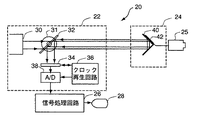
図1を参照して、この発明の第1の実施の形態に係る多チャンネル光学通信システム20は、光送信装置24および光受信装置22を含む。光送信装置24にはたとえばビデオカメラ25が接続される。光送信装置24はこのビデオカメラ25から受けた信号を光を用いて光受信装置22に伝送する。光受信装置22はこの光信号からビデオカメラ25の出力した映像信号を再生し信号処理回路26およびモニタ28に与えて表示する。
【0037】
光受信装置22は、やや広がりを持つ光束を光送信装置24に向けて出射するための光源30と、光源30の光路上に置かれ、光送信装置24側から反射してくる光を分岐するためのビームスプリッタ32と、ビームスプリッタ32によって分岐された光を受ける位置に配置されたCCD(固体撮像素子)34と、ビームスプリッタ32を中心軸周りに回転させることにより、ビームスプリッタ32で反射される光をCCD34の受光面上に導くためのステッピングモータ31と、CCD34の出力に基づいて、光送信装置24から送信されてくる信号中のクロック成分を再生するためのクロック再生回路36と、クロック再生回路36が再生するクロックに従ってCCD34が出力する信号を、クロック再生回路36の出力するクロック信号を逓倍した信号に従ってアナログ/デジタル変換するためのA/D(アナログ/デジタル)変換回路38とを含む。A/D変換回路38の出力は信号処理回路26に与えられ、モニタ28に表示される。
【0038】
光送信装置24は、1面が多数の画素に分割されたコーナキューブ40と、コーナキューブ40の上記した1面の各画素の反射/無反射をビデオカメラ25から与えられる映像信号に従って制御するための変調装置42とを含む。
【0039】
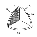
図2を参照して、コーナキューブ40は互いに垂直に組合された3つの反射面52、54および56を有する。これら反射面52、54および56のうちたとえば反射面52上が複数個の画素58に分割されている。各画素58は、変調装置42によって各画素ごとにその全反射/無反射が制御される。
【0040】
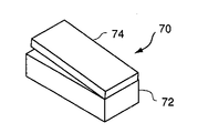
図4を参照して、図1に示す変調装置42は、図2に示される多数の画素58の配列と一致して配列された多数のデジタルマイクロミラーデバイス70を含む。各デジタルマイクロミラーデバイス70は、マイクロミラー74と、印加される電圧によってマイクロミラー74の方向を変化させるマイクロアクチュエータ72とを含む。たとえばデジタルマイクロミラーデバイス70に何ら電圧が印加されていない場合にはマイクロミラー74は図4に示されるようにマイクロアクチュエータ72と少し角度を持った方向を向き、デジタルマイクロミラーデバイス70に対して所定の電圧が印加されると図5に示されるようにマイクロミラー74はマイクロアクチュエータ72の上面に密着する。
【0041】
こうしたデジタルマイクロミラーデバイスについては「液晶より上?次世代ディスプレイの本命」(日経ビジネス、1999年11月15日号pp.60−64)に記載されている。
【0042】
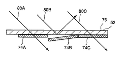
図6を参照して、反射面52は透明なガラス板76と、ガラス板76の裏面に配置された多数のデジタルマイクロミラーデバイス70(図4参照)とを含む。これらデジタルマイクロミラーデバイス70はいずれも、電圧が印加されているときにはマイクロミラーの反射面がガラス板76の裏面に密着し、電圧が印加されていないときにはマイクロミラー74がガラス板76の裏面から離れるような位置に配置されているものとする。マイクロミラー74の屈折率がガラス板76のそれと異なっていると、図6に示すように、電圧が印加されていないデジタルマイクロミラーデバイス70に対応する位置(マイクロミラー74Aおよび74C)では、光80Aおよび80Cは反射せず、電圧が印加されるデジタルマイクロミラーデバイスに対応する反射面74Bの位置では光80Bは反射される。
【0043】
したがって図2に示されるコーナキューブ40では、複数の画素58の各々について、対応するデジタルマイクロミラーデバイスに対する印加電圧を図1に示すビデオカメラ25からの映像信号に従って変化させることにより、各画素ごとに全反射/無反射を制御することができる。本実施の形態の装置では、こうして各画素ごとにコーナキューブ40における光の反射/無反射を制御し、それを光受信装置22側で各画素ごとに受光し復調することによって各画素ごとの信号を復調することができる。
【0044】
なおこの実施の形態のシステムではデジタルマイクロミラーデバイスを用いているが、この例のように光反射面を構成する透明板の背面に反射面74を配置する場合には、反射面74は必ずしも光を反射する性質のものである必要はない。透明板と反射面74との屈折率が相違してさえいれば、透明板の裏面に反射面74を密着させることにより光が全反射し、ある間隔を設ければ光が反射しなくなるからである。
【0045】
この第1の実施の形態に係る光通信システム20は以下のように動作する。なお光源30とコーナキューブ40とは、その相対的位置がほぼ一定となるように予め調整されているものとするが、後述するように光受信装置22および光送信装置24の一方またはその双方が移動体上にある場合のようにその相対的位置がずれたとしても、ビームスプリッタ32の回転角度を調整することにより、安定してCCD34が光送信装置24からの反射光を受光するようにできる。
【0046】
まず光源30がコーナキューブ40に向けて光束を出射する。この光はコーナキューブ40に入射し反射され、光源30に向けて戻る。このとき、コーナキューブ40上の1つの反射面52上の各画素58における反射/無反射をビデオカメラ25からの映像信号に従って制御することにより、ある画素に対応する位置では光が反射され、他の画素に対応する位置では光が反射されないことになる。
【0047】
ビームスプリッタ32はコーナキューブ40から反射されてくる光の光路を90°横方向に分岐させ、CCD34の受光面上に導く。CCD34は、予め定められた周期で受光と受光信号の出力とを繰返しているが、クロック再生回路36の制御によってその受光期間が、光送信装置24から送られてくる送信信号の1周期とできるだけ一致するように制御される。クロック再生回路36はCCD34の出力に基づいて上記したようにクロック信号を再生しCCD34の動作を制御するとともに、このクロック信号を所定数で逓倍した信号をA/D変換回路38に与える。A/D変換回路38は、CCD34から出力されるシリアルなアナログ信号を、クロック再生回路36から与えられる逓倍されたクロック信号に従ってデジタル変換し信号処理回路26に与える。信号処理回路26に与えられる信号は、結果としてビデオカメラ25から出力されるデジタルのシリアル信号と同様のものとなる。信号処理回路26によってこの信号を処理しモニタ28上に表示することにより、ビデオカメラ25で撮影した映像がモニタ28上に再生される。
【0048】
このとき、光送信装置24から光受信装置22に向けて送信される光信号は、各画素ごとに並列となった多チャンネルの光信号である。したがって1チャンネルで映像信号をシリアルに伝送する場合と比較して、各チャンネルごとの信号周期ははるかに長くなる。そのためCCD34による受光期間も長くすることができ、安定した復調を行なうことが可能となる。
【0049】
なお本実施の形態では図6に示すようにガラス板76上にマイクロミラー74が密着するように配置し、それによってガラス板76とマイクロミラー74の界面(全反射面)における全反射を制御した。しかし本発明はこうした構成には限定されず、たとえばマイクロミラー74を図2に示す反射面52自体を形成するようにマトリックス状に配置してもよい。この場合通常位置ではマイクロミラーが光を正しく反射し、所定の電圧が印加されるとマイクロミラーが位置を変え光を所定方向とは別の方向に反射するようにしてもよいし、その逆の構成にしてもよい。この例については図15、図16を参照して後述する。
【0050】
また、図6に示すようにマイクロミラー74をガラス板76と密着するように配置する場合、マイクロミラー74の密度がガラス板76の密度よりも高ければ前述のような全反射の制御が可能となる。マイクロミラー74の上面自体が反射能を有する必要はない。
【0051】
図3を参照して、光送信装置24の、光受信装置22に対する相対位置が図1に示す状態から変化した場合を想定する。前述したとおり光源30から出射される光ビームは広がりを持っている。そのため、光送信装置24の位置がずれたとしても一部の光ビームはコーナキューブ40によって反射されて戻ってくる。この反射光はコーナキューブ40への入射光と同じ向きであるから、図1の場合と比較してビームスプリッタ32への入射角度が変化している。そのため、ビームスプリッタ32の向きをそのままにしておくと、CCD34の受光面にこの反射光を導くことができない。
【0052】
この場合には、ステッピングモータ31によって、ビームスプリッタ32の角度を調整することにより、入射ビームの反射方向を調整すれば、コーナキューブ40からの反射光をCCD34の受光面に導くことができる。
【0053】
第2の実施の形態
上記した第1の実施の形態の光学通信システムでは、光通信自体はマルチチャンネルであるが、そのための入力信号および送信された後の復調信号はいずれもシリアル信号となっている。そのため結果として1チャンネル分の信号の送信が行なわれている。しかし本発明はそうした実施の形態のみに限定されるわけではない。たとえば複数チャンネルの信号を多数のチャンネルの光通信で送信し、受信側でそれぞれ別々の信号として復調することもできる。第2の実施の形態の光通信システム120はそのようなシステムである。
【0054】
図7を参照して、この光通信システム120は、光受信装置122および光送信装置124を含む。
【0055】
光送信装置124は、第1の実施の形態の光送信装置24と同様に1つの面が複数の画素に分割されたコーナキューブ140と、この各画素を別々に駆動するための変調装置142とを含む。
【0056】
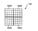
図8を参照して、変調装置142はこの実施の形態では4つの部分変調回路152A〜152Dを含む。そして図7に示されるように各部分変調回路152A〜152Dは別々の信号源125A〜125Dからの信号によって駆動される。この例の場合、各信号源125A〜125Dからシリアルに入力された信号を一旦図8に示すような形に配列された記憶素子に保持させた後、保持された信号を一斉に変調装置142の各素子部分に与える。こうすることによりシリアルに入力された信号をパラレルに、かつその信号周期を長くして転送することができる。
【0057】
光受信装置122は、第1の実施の形態の場合と同様に配置された光源30およびビームスプリッタ32と、ビームスプリッタ32により分岐された光束を受光するためのCCD134と、CCD134の出力に基づいてクロック信号を再生しCCD134による受光期間を制御するとともに、このクロック信号を逓倍した信号を出力するためのクロック再生回路138と、CCD134のそれぞれ4つの領域から出力されるシリアル信号をパラレルに受け、クロック再生回路138から与えられる逓倍されたクロック信号に従ってアナログ/デジタル変換するためのA/D変換回路136A〜136Dとを含む。これらA/D変換回路136A〜136Dの出力はそれぞれ信号源125A〜125Dに対応する送信先126A〜126Dに与えられる。
【0058】
この第2の実施の形態の光通信システム120は以下のように動作する。各信号源125A〜125Dはそれぞれ独立に変調装置142に対して信号を与える。変調装置142の部分変調回路152A〜152Dはこれらシリアルに与えられた信号を順次各画素ごとに格納し、あるタイミングで対応するデジタルマイクロミラーデバイスに与える。その結果光源30から出射される光がコーナキューブ140で反射される際に、各画素ごとにその反射/無反射が制御される。こうして元の信号により変調された光がビームスプリッタ32に入射し、さらにCCD134の受光面上に入射する。クロック再生回路138はCCD134の出力に基づいてクロック信号を再生しCCD134の出力周期を制御する。同時にクロック再生回路138はこのクロック信号を所定数で逓倍した信号を作り、A/D変換回路136A〜136Dに与える。各A/D変換回路136A〜136Dは、CCD134の対応する1/4面からシリアルに出力される信号をデジタル信号に変換し対応する送信先126A〜126Dに与える。こうして、複数の信号源125A〜125Dから与えられた信号が、1つの多チャンネル光通信路を介して同時に光受信装置122に送信され、それぞれ対応の送信先126A〜126Dに独立に送信される。
【0059】
この第2の実施の形態では、画像信号ではないシリアル信号をまとめた形で光通信することができる。この場合にも光通信自体は多チャンネルで行なわれるため、各信号をシリアルで通信する場合と比較してシンボル期間を長くすることができ、安定した光通信を行なうことができる。
【0060】
第3の実施の形態
第1の実施の形態の装置では、一旦ビデオカメラ25(図1参照)から出力されたシリアルな映像信号を変調装置42に与え、多チャンネルの信号として光通信により送信した。しかし本発明は、画像の伝送に使用した場合に限っても第1の実施の形態の形に限定されるものではない。たとえばこの第3の実施の形態の光通信システム220のように、画像信号の入力をパラレルに行なうこともできる。
【0061】
図9を参照して、この光通信システム220は光送信装置224と光受信装置222とを含む。
【0062】
光送信装置224はコーナキューブ240と、コーナキューブ240の1面の裏に配置され、固体撮像素子と上記したデジタルマイクロミラーデバイスとが一体に成形された受光・変調装置242と、受光・変調装置242のCCDの撮像面(受光面)上に被写体の光学像を結像させるための光学系246と、受光・変調装置242による受光期間と、デジタルマイクロミラーデバイスへの電荷の転送とを制御するためのドライバ装置248とを含む。
【0063】
ドライバ装置248は、ある期間に受光/変調装置242の受光面に生成された電荷を、一斉にデジタルマイクロミラーデバイスに与えることによりデジタルマイクロミラーデバイスの各反射面の向きを制御する。同時にドライバ装置248は受光面上の電荷を消去し、次の期間の受光を行なうという作業を繰返す。
【0064】
光受信装置222は、既に述べた光源30およびビームスプリッタ32と、ビームスプリッタ32によって分岐された光を受光する位置に配置されたCCD234と、CCD234の各受光素子からの電荷を並列に受け保持し、シリアルに出力するための固体撮像素子と同様の構成を有する電荷転送素子236と、CCD234の出力に基づいて送信信号に含まれるクロック成分を再生し、CCD234と電荷転送素子236の動作を制御するためのクロック信号を生成し出力するとともに、このクロック信号を逓倍した信号を出力するためのクロック再生回路238と、クロック再生回路238から与えられる逓倍されたクロック信号に従って、電荷転送素子236から出力されるシリアルの信号をデジタル信号に変換するためのA/D変換回路238とを含む。A/D変換回路238の出力は第1の実施の形態の場合と同様に信号処理回路26に与えられ、さらにモニタ28により表示される。
【0065】
この第3の実施の形態の光通信システム220は以下のように動作する。ドライバ装置248は受光/変調装置242の受光面の電荷を消去し受光を開始する。光学系246により受光面上に被写体の光学像が形成され、受光面上の光電変換素子はそれぞれ入射光量に応じた電荷を蓄積する。ドライバ装置248は所定のタイミングでこの電荷を対応するデジタルマイクロミラーデバイスに転送するとともに、CCDの受光素子上の電荷を消去する。このドライバ装置248の制御により、受光/変調装置242を構成する各マイクロミラーデバイスの反射面はそれぞれ全反射位置または無反射位置に変化する。
【0066】
光受信装置222の光源30から出射された光はコーナキューブ240により反射されビームスプリッタ32に入射する。このとき、コーナキューブ240の1面において、受光・変調装置242によりある画素に対応する位置では光の反射はなく、他の画素に対応する位置では光の反射が行なわれる。その結果コーナキューブ240からビームスプリッタ32に向けて反射される光は、これら各素子の状態に応じて各反射光が変調された多チャンネルの光束となっている。ビームスプリッタ32で反射されたこの光束がCCD234上に入射することにより、被写体の光学像により形成されるのと同様の電荷の分布がCCD234上に形成される。クロック再生回路238は、1シンボル区間に対応する期間だけCCD234で電荷を蓄積した後各電荷をパラレルに電荷転送素子236に転送する。同時にクロック再生回路238はCCD234上の各光電変換素子の電荷を消去する。
【0067】
電荷転送素子236はクロック再生回路238から与えられるクロック信号に応じて、蓄積された電荷をシリアルに出力しA/D変換回路238に与える。A/D変換回路238はクロック再生回路238から出力される逓倍されたクロック信号に従ってこの信号をデジタル信号に変換し信号処理回路26に与える。
【0068】
こうしてこの第3の実施の形態の光通信システムでは、光送信装置側で受光面上に形成された被写体の光学像を直接パラレルの信号に変換し、それをさらにパラレルの光信号として光受信装置側に転送することができる。この場合にも、受信側では1チャンネルを用いてパラレルにこの映像信号を送信する場合と比較してシンボル区間が長くなるため、安定して光通信を行なうことができる。
【0069】
なお図9に示す例では光学系246の位置が受光面上に被写体の像を結像するような位置に固定されている。しかし本発明はこれには限定されない。受光面上に被写体の光学像が結ばれることを条件として、光学系の配置はさまざまに変えることができる。
【0070】
第4の実施の形態
第1〜第3の実施の形態からも明らかなように、この光通信システムは複数の信号源からの信号をパラレルに送信することができる。そのためのチャンネル数の最大数は、コーナキューブ上に形成された各画素(以下に述べるように、反射面での全反射条件を制御する機能を持つもので、以下「全反射条件制御素子」と呼ぶ。)の数と同じである。もちろん反射面の周辺位置に存在する全反射条件制御素子については利用可能でない場合もあるが、コーナキューブの中央付近に設けられている全反射条件制御素子のみを用いてもかなり多数のチャンネルを用いた光通信が行なえる。この第4の実施の形態の光通信システムはそのように各チャンネルごとに独立した通信を行なうことができるものである。
【0071】
図10を参照してこの第4の実施の形態に係る光通信システム320は、光送信装置324および光受信装置322を含む。
【0072】
光送信装置324は、多数の信号源からの信号を集めるための集積装置344と、多数のデジタルマイクロミラーデバイスを含む変調装置342と、集積装置344により集積された各信号をそれぞれ独立に変調装置342の各デジタルマイクロミラーデバイスと接続するための接続線346と、変調装置342を駆動するためのドライバ装置348と、変調装置342がその反射面の1つの裏面に配置されたコーナキューブ340とを含む。
【0073】
光受信装置322は、光源30およびビームスプリッタ32と、ビームスプリッタ32により分岐された光束を受光する位置に配置されたCCD334と、CCD334の出力に基づいてCCD334を駆動するためのクロック信号を再生するためのクロック再生回路338と、CCD334の各光電変換素子の出力をパラレルに受けて増幅し、デジタル信号に変換して分岐して出力するための分岐回路336とを含む。
【0074】
クロック再生回路338は、1シンボル期間の間CCD334で光電変換を行なわせ、1期間が終了すると各光電変換素子の信号をパラレルに分岐回路336に出力させる。同時にクロック再生回路338はCCD334の各光電変換素子の電荷を消去し、次の期間の光電変換に備える処理を行なう。
【0075】
この第4の実施の形態の光通信システム320は次のように動作する。それぞれ別個の多数の信号源から集められた信号は集積装置344により集積され接続線346によって変調回路342に与えられる。変調回路342はドライバ装置348の制御に従って、所定区間ごとに接続線346から与えられる信号を取込み、対応するデジタルマイクロミラーデバイスに与える。各デジタルマイクロミラーデバイスはこれら信号の値に従ってその反射面の位置を変化させる。
【0076】
光源30から出射された光はコーナキューブ340に入射し反射する。このときコーナキューブ340の1つの反射面上において、デジタルマイクロミラーデバイスの反射面の位置に応じて、各素子ごとに反射/無反射が制御される。したがってコーナキューブ340からビームスプリッタ32に向けて反射される光は、各チャンネルごとに変調装置342によって変調された信号を搬送する多チャンネルの光信号となっている。
【0077】
ビームスプリッタ32によって反射されたこの光束はCCD334上に入射し、各素子に対応した電荷をCCD334の各素子ごとに生成する。クロック再生回路338の制御により各光電変換素子の出力は分岐回路336に与えられ、デジタル信号に変換されて各対応する送信先に向けて送信される。
【0078】
この第4の実施の形態の光通信システムでは、多数の信号源とコーナキューブ上の全反射条件制御素子とを1対1の関係とすることにより、全反射条件制御素子の数と同じ数だけの光通信チャンネルを設けることができる。その結果、非常にコンパクトに数多くのチャンネル信号を安定に送信することができるという効果を奏する。たとえば全反射条件制御素子の配列が1000×1000であれば提供されるチャンネル数は1000×1000=1,000,000となり、光通信を用いた広帯域の通信を行なうことができる。
【0079】
全反射条件制御素子の他の例
以上の説明では、光反射面の表面にデジタルマイクロミラーデバイスを、または光反射面を構成する透明板の裏面にデジタルマイクロアクチュエータを配置することにより全反射条件制御素子を形成したコーナキューブを用いている。しかし全反射条件制御素子の構成はこうしたものには限定されない。その一例を図11に示す。
【0080】
図11を参照して、このコーナキューブ400のひとつの反射面上には、複数個の、プリズムの全反射条件を制御する全反射条件制御素子402が配列されている。図12に示されるように、各全反射条件制御素子402は、透明カプセル404と、この透明カプセル404の中に封入された不透明な磁性流体410と、透明カプセル404のそれぞれ半分の領域に別々に形成され、電流が加えられると磁場を発生する二つの電磁石420および422とを含む。
【0081】
たとえば図12における電磁石420に電流を通ずると磁場が生じ、磁性流体410は電磁石420の方向に集まる。その結果、磁性流体410のない、透明な部分412が形成される。逆に電磁石422に電流を通ずると磁性流体410は電磁石422の方向に集まる。その結果図12とは逆に参照符号410で示した領域が透明になり、その結果プリズム面に磁性流体が接する領域がなくなり、この領域ではプリズムは全反射状態となる。また、参照符号412で示した領域が不透明になるので、磁性流体がプリズム面に接する部分となり、全反射が阻害その結果、この全反射条件制御素子402においては、電磁石420および422のいずれに電流を通ずるかにしたがって異なる反射率の分布ができ、これによって入射光を変調して反射することが可能になる。
【0082】
なお、図12に示した例では磁性流体を用いたが、たとえばその方向が同一方向固定された多数のごく小さな棒磁石を細長い管に封入し、その管を多数束ねたものを用いたものを磁性流体に代えて用いてもよい。この場合、透明カプセル404の一端にたとえばS極の磁場を置くことにより、これらすべての棒磁石がそれら自身の磁極とこのS極との間の磁力によって同一方向に移動し、このS極に代えてN極をおけばこんどはこれらすべての棒磁石が反対方向に移動する。その結果、磁性流体を用いた場合と同様に全反射制御素子群における全反射部分の分布を変化させることができる。
【0083】
なお、このようにごく小さな棒磁石を用いる場合、透明カプセル404の両端に同じ磁性の磁極を置くと、棒磁石に対して一方の磁極からは引力が、他方の磁極からは斥力が働く。この結果、この磁極の磁性を変化させたときの棒磁石の移動が早くなる。そのためそうした構成では磁極を一つしか使用しない場合と比較してレスポンスが向上するという効果がある。
【0084】
全反射条件制御素子のさらに他の例
全反射条件制御素子の他の例として、電流により制御されるのではなく、光により制御されるマイクロアクチュエータを用いることもできる。特にポリジアセチレンと呼ばれる高分子化合物のように、光があたると変形するような性質を持つ物質を用いると、応答速度の高いアクチュエータを実現できる。
【0085】
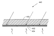
図13に、そうした光により制御されるマイクロアクチュエータを備えた全反射条件制御素子440の断面図を示す。図13を参照して、このマイクロアクチュエータは、コーナキューブのプリズム450の全反射面に配置されており、通常時にプリズム450の全反射面に密着するように配置される、薄くやや弾力のある、プリズム450の密度よりも高い密度を持つ物質からなる全反射制御体452と、全反射制御体452の、プリズム450と密着している面と反対側の面に接着された、前述のポリジアセチレンの薄膜454とを含む。全反射制御体452は、その周縁部分においてガラス面450の裏面に接着されている。全反射制御体452としては、プリズム450の全反射面に密着できることができ、かつ後述するように変形したときに、全反射面との間に生じる空隙が全反射を阻害する程度の大きさとなる弾力性を有するものが用いられる。
【0086】
図13に示されるように、第1の状態では全反射制御体452はプリズム450の全反射面に密着している。そのため、ガラス板450に入射する光はプリズム450の全反射面で全反射されず、全反射制御体452側に透過する。すなわち光は全反射面では反射されない。
【0087】
ポリジアセチレンは、波長が450〜550ナノメートルの光を当てると体積が3%ほど増え、350〜400ナノメートルの波長を持つ光を当てると元に戻る性質があることが知られている。
【0088】
そこで、図13の状態において、全反射をさせる部分に対応する全反射条件制御素子には、裏面から450〜550ナノメートルの波長を持つ光をあてる。この部分では、ポリジアセチレンの薄膜454は体積が増加し、図14の中央に示すようにプリズム450の全反射面との間に空隙が生じる。したがって当該全反射条件制御素子に入射する光は全反射される。
【0089】
一方、全反射をさせない部分に対応する全反射条件制御素子には、裏面から350〜400ナノメートルの波長を持つ光を当てる。すると、図14の左右に示されるように、ポリジアセチレンの薄膜454は体積が減少し、したがって全反射制御体452とともに全反射条件制御素子の全体が、その中央部がガラス面450に密着する様に変形する。その結果プリズム450の全反射面に入射する光は全反射されない。
【0090】
このように光により変形する性質を持つ物質によって反射条件制御素子を駆動するようにすると、応答速度が高く、構造も比較的単純である。また、反射条件制御素子を光により駆動するため、反射条件制御素子を信号で駆動するための配船が不要となる。したがって装置を一層小型化することができ、高密度で多チャンネル光通信を実現することが可能となる。
【0091】
反射条件制御素子の例
図2に示すコーナキューブ40の変形例を図15および図16に示す。図15に示す例では、コーナキューブ500は、図2に示すコーナキューブ40と比較して、図2における反射面52に替えて、光を反射しない物質からなる、反射面54および56と直交するように設けられた基板510と、基板510の、反射面54および56に面する面上にマトリクス状に配列された複数個のマイクロミラーデバイス512とを含む点が異なる。基板510は透明な物質でも、不透明な物質でもよい。また光を反射する物質からなっていてもよい。
【0092】
複数個のマイクロミラーデバイス512の各々は、いずれもその方向が第1の方向と第2の方向とに制御可能な反射面を有する。第1の方向とは、デジタルミラーマイクロデバイスの反射面が、反射面54および56と直交する面に含まれるような方向である。第2の方向は、第1の方向と異なる方向、すなわちマイクロミラーデバイスの反射面が反射面54および56と直交するような方向以外であればどのような方向でもよい。
【0093】
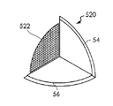
このコーナキューブ500を用いると、デジタルマイクロデバイスの反射面が第1の方向を向いているときにはそのデジタルマイクロデバイスの反射面に入射する光は、入射方向と平行に反射される。そしてデジタルマイクロデバイスの反射面が第2の方向を向いているときには、入射方向と異なる方向に反射される。したがって第1の実施の形態の場合と同様に、このコーナキューブ500を多チャンネル光通信に用いることができる。
【0094】
また、図16に示されるコーナキューブ520は、図15に示されるものと比較して、基板510を取り除いている点に特徴があり、マトリクス状に配列された複数個のデジタルマイクロデバイス522によって反射面を構成している。この場合にも、デジタルマイクロデバイス522の各々の反射面の方向を図15の場合と同様の第1の方向と第2の方向とに制御できれば、多チャンネル光通信に用いることができる。
【0095】
今回開示された実施の形態はすべての点で例示であって制限的なものではないと考えられるべきである。本発明の範囲は上記した説明ではなくて特許請求の範囲によって示され、特許請求の範囲と均等の意味および範囲内でのすべての変更が含まれることが意図される。
【図面の簡単な説明】
【図1】 この発明の第1の実施の形態に係る光通信システムのブロック図である。
【図2】 コーナキューブの外観を示す図である。
【図3】 第1の実施の形態に係る光通信システムにおいてビームスプリッタの角度を変えたときのブロック図である。
【図4】 デジタルマイクロミラーデバイスの動作を説明するための図である。
【図5】 デジタルマイクロミラーデバイスの動作を説明するための図である。
【図6】 デジタルマイクロミラーデバイスを用いた反射/無反射の制御を説明するための図である。
【図7】 この発明の第2の実施の形態に係る光通信システムのブロック図である。
【図8】 第2の実施の形態で用いられる部分変調回路の配置を示す図である。
【図9】 この発明の第3の実施の形態に係る光通信システムのブロック図である。
【図10】 この発明の第4の実施の形態に係る光通信システムのブロック図である。
【図11】 全反射条件制御素子を有する他のコーナキューブ面の他の例を示す図である。
【図12】 図11の例で用いられる全反射条件制御素子群の概略図である。
【図13】 全反射条件制御素子のさらに他の例を示す断面図である。
【図14】 図13に示す全反射条件制御素子の動作原理を示す断面図である。
【図15】 デジタルマイクロミラーデバイスを用いたコーナキューブの変形例を示す斜視図である。
【図16】 デジタルマイクロミラーデバイスを用いコーナキューブのさらに他の変形例を示す斜視図である。
【符号の説明】
20,120,220,320 光通信システム、22,122,222,322 光受信装置、24,124,224,324 光送信装置、30 光源、32 ビームスプリッタ、34,134,234,334 CCD、40,140,240,340 コーナキューブ、42,142,342 変調装置、70デジタルマイクロミラーデバイス、242 受光・変調装置。[0001]
BACKGROUND OF THE INVENTION
This invention uses light as a mediumHikariMulti-channel using recursive reflectors represented by corner cubesHikariSystem and optical transmitter for the sameIn placeRelated.
[0002]
[Prior art]
Research has been conducted on communication systems using light that are not subject to legal restrictions such as radio communications by replacing communications using radio waves subject to various legal restrictions. An example of such an optical communication system is “about speed-up of light intensity modulation using attenuated total reflection in a corner cube” (Toshihiro Tsumura et al., IEICE Technical Report SANE 94-91, SAT 94-91, pp. 111-114). Is disclosed.
[0003]
The communication system disclosed here is a bidirectional spatial optical communication system using a laser, and a laser oscillator is provided on one side and a corner cube is provided on the other side. By modulating the laser beam emitted from the laser oscillator with an external signal, the signal can be demodulated from the received laser beam on the light receiving side.
[0004]
The corner cube reflects this incident light to the laser oscillator side. At this time, as a characteristic of the corner cube, light incident from a certain direction is reflected in the same direction. Therefore, the reflected light always reaches very close to the laser oscillator. A modulator for modulating the reflected light is provided on one surface of the corner cube depending on whether the reflection on the corner cube surface is total reflection or non-reflection. Information can be placed on the reflected light by driving the modulator with an external signal. A light receiving sensor for receiving the reflected light is provided on the laser oscillator side, and a signal transmitted from the corner cube side can be demodulated from the output of the light receiving sensor.
[0005]
[Problems to be solved by the invention]
However, although the above-described communication system can perform bi-directional optical communication, there is a problem that only one channel can be assigned for each transmission / reception. In particular, when image information or the like is transmitted by optical communication, the amount of information becomes very large. Therefore, if only one channel is used, the signal interval per symbol is shortened, and particularly in optical communication using a photoelectric conversion element. In some cases, the demodulation becomes difficult.
[0006]
As a medium for a multi-channel communication system using light, there is a medium using an optical fiber. When optical fibers are used, optical communication can be performed efficiently, but there is a problem that an optical fiber must be spread over a wide area and enormous funds are required to construct an infrastructure. In addition, the optical fiber is not effective in the mutual communication with the mobile body and the mutual space communication between the mobile body and the mobile body.
[0007]
SUMMARY OF THE INVENTION Therefore, an object of the present invention is to provide a multi-channel capable of performing large-capacity optical communication at low cost.HikariSystemandOptical transmitter for that purposePlaceIs to provide.
[0008]
[Means for Solving the Problems]
BookinventionThe first aspect ofThe multi-channel optical communication system according to the present invention includes a retroreflective unit that reflects incident light in the same direction as the incident direction, and a light that is reflected by the retroreflective unit.Multi-channelAn optical transmitter including a modulating means for modulating based on a transmission signal, a light emitting means for emitting light, and light modulated by the modulating means from light emitted from the light emitting means and reflected by the retroreflecting meansMulti-channelAnd an optical receiver including a demodulator for demodulating the transmission signal.Multi-channel optical communication system.The modulation means is on the reflection surface of the retroreflection means.In response to multi-channel transmission signalsA plurality of total reflection condition control elements that are arranged and can independently control the reflection of light, and each of the total reflection condition control elements,Of the multi-channel transmission signals, the channel corresponding to each reflection condition control elementDrive means for independently controlling based on the transmission signal, and the demodulating means includes a plurality of total reflection condition control elements arranged in correspondence with the arrangement of the plurality of total reflection condition control elements for receiving the reflected light. Light receiving means having a plurality of light receiving elements and outputs of a plurality of light receiving elementsOf the channel corresponding to the total reflection condition control element corresponding to each light receiving element in the multi-channel transmission signal.Transmission signalRespectivelyMeans for reconstructing.
[0009]
A plurality of total reflection condition control elements can independently control the reflection of light. Therefore, by controlling the reflection of each of the plurality of total reflection condition control elements with different information, a signal beam bundle modulated by different information from the optical transmission device to the optical reception device is obtained. Can be transmitted over multiple channels. Since optical communication is performed using multiple channels, the symbol period can be extended, and the light receiving means of the optical receiver can perform stable photoelectric conversion.
[0014]
Claim1Multi-channel optical communication system according to the inventionThenThe total reflection condition control element is arranged on the reflection surface, and the light reflectance in the total reflection condition control element is obtained by moving the magnetic substance in the transparent capsule encapsulated in the transparent capsule by the magnetic force. And a magnetic force generating means for changing the distribution of.
[0015]
By changing the distribution of the opaque magnetic material by the magnetic force, total reflection and non-reflection on the reflecting surface can be controlled. Since total reflection is performed at the time of reflection, stable communication can be performed with little loss of light and relatively low risk of transmission errors.
[0016]
Claim2Multi-channel optical communication system according to the inventionThenThe total reflection condition control element is arranged so as to face the total reflection surface of the retroreflective means from the direction opposite to the direction in which the light is incident on the total reflection surface of the retroreflective means, and is irradiated with light of a specific wavelength. And a light driving element that changes the shape between a first shape that is in close contact with the total reflection surface and a second shape in which a gap is formed between the total reflection surface, The reflection of the total reflection surface is controlled by irradiating light with a specific wavelength.
[0017]
Since the total reflection condition control element is driven by light, wiring for sending a signal to the total reflection condition control element becomes unnecessary. The configuration of the apparatus is simplified, the total reflection condition control element can be reduced in size, and the density can be increased. Therefore, the number of channels that can be used increases.
[0018]
The present inventionOther aspects ofAn optical transmitter for a multi-channel optical communication system according to the present invention includes a retroreflective unit that reflects incident light in the same direction as the incident direction, and a light that is reflected by the retroreflective unit.Multi-channelOptical transmission device including modulation means for modulating based on transmission signalBecauseThe modulation means is on the reflection surface of the retroreflection means.In response to multi-channel transmission signalsA plurality of reflection condition control elements arranged and capable of independently controlling the reflection of light, and each of the reflection condition control elements,Of the multi-channel transmission signals, the channel corresponding to each reflection condition control elementDriving means for independently controlling based on the transmission signal.
[0019]
MultipleThe opposite ofIrradiation condition control elements can control the reflection of light independently of each other. Therefore, these multipleThe opposite ofBy controlling the reflection of the projection condition control element with separate information, the signal is transmitted in multiple channels from the optical transmitter to the optical receiver as a bundle of light beams modulated with different information. Can do. Since optical communication is performed using multiple channels, the symbol period can be extended, and the light receiving means of the optical receiver can perform stable photoelectric conversion.
[0028]
Claim3Transmitter for a multi-channel optical communication system according to the inventionThenThe reflection condition control element is arranged on the light reflection surface, and the opaque magnetic substance enclosed in the transparent capsule and the light reflectance distribution in the reflection condition control element by moving the magnetic substance in the transparent capsule by magnetic force. And a magnetic force generating means for changing.
[0029]
By changing the distribution of the opaque magnetic material by the magnetic force, total reflection and non-reflection on the reflecting surface can be controlled. Since total reflection is performed at the time of reflection, stable communication can be performed with little loss of light and relatively low risk of transmission errors.
[0030]
Claim4Transmitter for a multi-channel optical communication system according to the inventionThenThe reflection condition control element is disposed on the back surface of the transparent plate constituting the reflection surface of the retroreflective means, and responds to the irradiation with the light having a specific wavelength, and is in close contact with the back surface, Including a light driving element that changes its shape with the second shape in which a gap is formed, and by irradiating the light driving element with light of a specific wavelength, reflection on the back surface of the transparent plate Be controlled.
[0031]
By lightAntiBecause the shooting condition control element is driven, AntiWiring for sending a signal to the shooting condition control element becomes unnecessary. The equipment configuration is simplified, AntiThe irradiation condition control element can be miniaturized and the density can be increased. Therefore, the number of channels that can be used increases.
[0036]
DETAILED DESCRIPTION OF THE INVENTION
First embodiment
With reference to FIG. 1, a multi-channel
[0037]
The
[0038]
The
[0039]
Referring to FIG. 2,
[0040]
Referring to FIG. 4, the
[0041]
Such a digital micromirror device is described in “Beyond liquid crystal? A favorite of next-generation displays” (Nikkei Business, November 15, 1999, pp. 60-64).
[0042]
Referring to FIG. 6, the reflecting
[0043]
Therefore, in the
[0044]
Although the digital micromirror device is used in the system of this embodiment, when the reflecting
[0045]
The
[0046]
First, the
[0047]
The
[0048]
At this time, the optical signal transmitted from the
[0049]
In this embodiment, as shown in FIG. 6, the
[0050]
Further, when the
[0051]
Referring to FIG. 3, a case is assumed in which the relative position of
[0052]
In this case, the reflected light from the
[0053]
Second embodiment
In the optical communication system according to the first embodiment described above, the optical communication itself is multi-channel, but both the input signal and the demodulated signal after transmission are serial signals. As a result, signals for one channel are transmitted. However, the present invention is not limited to such an embodiment. For example, signals of a plurality of channels can be transmitted by optical communication of many channels and demodulated as separate signals on the receiving side. The
[0054]
Referring to FIG. 7, the
[0055]
Similar to the
[0056]
Referring to FIG. 8,
[0057]
The
[0058]
The
[0059]
In the second embodiment, optical communication can be performed in a form in which serial signals that are not image signals are combined. In this case as well, since the optical communication itself is performed with multiple channels, the symbol period can be lengthened compared to the case where each signal is communicated serially, and stable optical communication can be performed.
[0060]
Third embodiment
In the apparatus of the first embodiment, a serial video signal once output from the video camera 25 (see FIG. 1) is given to the
[0061]
Referring to FIG. 9, the
[0062]
The
[0063]
The
[0064]
The
[0065]
The
[0066]
Light emitted from the
[0067]
The
[0068]
Thus, in the optical communication system according to the third embodiment, the optical image of the subject formed on the light receiving surface on the optical transmission device side is directly converted into a parallel signal, which is further converted into a parallel optical signal. Can be transferred to the side. Also in this case, since the symbol section becomes longer as compared with the case where the video signal is transmitted in parallel using one channel on the receiving side, the optical communication can be performed stably.
[0069]
In the example shown in FIG. 9, the position of the optical system 246 is fixed at a position where an image of the subject is formed on the light receiving surface. However, the present invention is not limited to this. The arrangement of the optical system can be variously changed on condition that an optical image of the subject is formed on the light receiving surface.
[0070]
Fourth embodiment
As is clear from the first to third embodiments, this optical communication system can transmit signals from a plurality of signal sources in parallel. For this purpose, the maximum number of channels is the number of pixels formed on the corner cube (which has the function of controlling the total reflection condition on the reflection surface as described below, and is referred to as the “total reflection condition control element” hereinafter). Is the same as the number of Of course, it may not be possible to use the total reflection condition control element in the peripheral position of the reflection surface, but even if only the total reflection condition control element provided near the center of the corner cube is used, a considerably large number of channels are used. Optical communication. In this way, the optical communication system of the fourth embodiment can perform independent communication for each channel.
[0071]
Referring to FIG. 10, the
[0072]
The
[0073]
The
[0074]
The
[0075]
The
[0076]
The light emitted from the
[0077]
This light beam reflected by the
[0078]
In the optical communication system of the fourth embodiment, the number of signal sources and the total reflection condition control elements on the corner cube are in a one-to-one relationship, so that the number of total reflection condition control elements is the same as the number of total reflection condition control elements. Optical communication channels can be provided. As a result, it is possible to stably transmit a large number of channel signals in a very compact manner. For example, if the arrangement of the total reflection condition control elements is 1000 × 1000, the number of channels provided is 1000 × 1000 = 1,000,000, and broadband communication using optical communication can be performed.
[0079]
Other examples of total reflection condition control elements
In the above description, a digital micromirror device is formed on the surface of the light reflecting surface, or a corner cube having a total reflection condition control element formed by arranging a digital microactuator on the back surface of the transparent plate constituting the light reflecting surface is used. Yes. However, the configuration of the total reflection condition control element is not limited to this. An example is shown in FIG.
[0080]
Referring to FIG. 11, a plurality of total reflection
[0081]
For example, when a current is passed through the
[0082]
In the example shown in FIG. 12, a magnetic fluid is used. For example, a magnetic fluid in which a number of very small bar magnets whose directions are fixed in the same direction are sealed in an elongated tube and a large number of the tubes are bundled is used. A magnetic fluid may be used instead. In this case, for example, by placing a magnetic field of S pole on one end of the
[0083]
When such a very small bar magnet is used, if the same magnetic pole is placed on both ends of the
[0084]
Other examples of total reflection condition control elements
As another example of the total reflection condition control element, a microactuator that is not controlled by current but controlled by light can be used. In particular, an actuator having a high response speed can be realized by using a material having a property of being deformed when exposed to light, such as a polymer compound called polydiacetylene.
[0085]
FIG. 13 shows a cross-sectional view of a total reflection
[0086]
As shown in FIG. 13, the total
[0087]
It is known that polydiacetylene has the property of increasing its volume by about 3% when irradiated with light having a wavelength of 450 to 550 nanometers and returning to its original state when irradiated with light having a wavelength of 350 to 400 nanometers.
[0088]
Therefore, in the state of FIG. 13, light having a wavelength of 450 to 550 nanometers from the back surface is applied to the total reflection condition control element corresponding to the total reflection portion. In this portion, the volume of the polydiacetylene
[0089]
On the other hand, light having a wavelength of 350 to 400 nanometers is applied to the total reflection condition control element corresponding to the portion where total reflection is not performed. Then, as shown on the left and right of FIG. 14, the volume of the polydiacetylene
[0090]
In this way, depending on the substance that has the property of being deformed by light,AntiWhen the shooting condition control element is driven, the response speed is high and the structure is relatively simple. Also, AntiTo drive the lighting condition control element with light, AntiThere is no need for ship assignment to drive the firing condition control element with a signal. Therefore, the apparatus can be further miniaturized, and multi-channel optical communication can be realized with high density.
[0091]
Example of reflection condition control element
A modification of the
[0092]
Each of the plurality of
[0093]
When this
[0094]
Also, the
[0095]
The embodiment disclosed this time should be considered as illustrative in all points and not restrictive. The scope of the present invention is defined by the terms of the claims, rather than the description above, and is intended to include any modifications within the scope and meaning equivalent to the terms of the claims.
[Brief description of the drawings]
FIG. 1 is a block diagram of an optical communication system according to a first embodiment of the present invention.
FIG. 2 is a diagram showing an appearance of a corner cube.
FIG. 3 is a block diagram when the angle of the beam splitter is changed in the optical communication system according to the first embodiment.
FIG. 4 is a diagram for explaining the operation of the digital micromirror device.
FIG. 5 is a diagram for explaining the operation of the digital micromirror device.
FIG. 6 is a diagram for explaining reflection / non-reflection control using a digital micromirror device.
FIG. 7 is a block diagram of an optical communication system according to a second embodiment of the present invention.
FIG. 8 is a diagram showing an arrangement of partial modulation circuits used in the second embodiment.
FIG. 9 is a block diagram of an optical communication system according to a third embodiment of the present invention.
FIG. 10 is a block diagram of an optical communication system according to a fourth embodiment of the present invention.
FIG. 11 is a view showing another example of another corner cube surface having a total reflection condition control element.
12 is a schematic diagram of a total reflection condition control element group used in the example of FIG.
FIG. 13 is a cross-sectional view showing still another example of the total reflection condition control element.
14 is a cross-sectional view showing the operation principle of the total reflection condition control element shown in FIG.
FIG. 15 is a perspective view showing a modified example of a corner cube using a digital micromirror device.
FIG. 16 is a perspective view showing still another modified example of the corner cube using the digital micromirror device.
[Explanation of symbols]
20, 120, 220, 320 Optical communication system, 22, 122, 222, 322 Optical receiver, 24, 124, 224, 324 Optical transmitter, 30 Light source, 32 Beam splitter, 34, 134, 234, 334 CCD, 40 , 140, 240, 340 Corner cube, 42, 142, 342 Modulator, 70 digital micromirror device, 242 Light receiving / modulating device.
Claims (4)
前記再帰反射手段によって反射される光を、多チャンネルの伝送信号に基づいて変調するための変調手段とを含む光送信装置と、
光を出射する光出射手段と、
前記光出射手段から出射され前記再帰反射手段によって反射された光から、前記変調手段によって変調された前記多チャンネルの伝送信号を復調するための復調手段とを含む光受信装置とを含む多チャンネル光通信システムであって、
前記変調手段は、
前記再帰反射手段の反射面上に、前記多チャンネルの伝送信号に対応して配列され、各々独立に光の反射を制御することが可能な複数個の全反射条件制御素子と、
前記全反射条件制御素子の各々を、前記多チャンネルの伝送信号の内、各前記反射条件制御素子に対応するチャンネルの伝送信号に基づいて独立に制御するための駆動手段とを含み、
前記復調手段は、
前記反射された光を受光するための、前記複数個の全反射条件制御素子の配列に対応して配列された複数個の受光素子を有する受光手段と、
前記複数個の受光素子の出力から、前記多チャンネルの伝送信号の内で各受光素子に対応する前記全反射条件制御素子に対応するチャンネルの伝送信号をそれぞれ再構築するための手段とを含み、
前記全反射条件制御素子は、前記反射面上に配置され、透明カプセル中に封入された不透明な磁性体と、前記透明カプセル中の前記磁性体を磁力により移動させることにより前記全反射条件制御素子における光の反射率の分布を変化させるための磁力発生手段とを含む、多チャンネル光通信システム。Retroreflecting means for reflecting incident light in the same direction as the incident direction;
An optical transmission device including modulation means for modulating light reflected by the retroreflecting means based on a multi-channel transmission signal;
Light emitting means for emitting light;
A multi-channel light including a light receiving device including a demodulating means for demodulating the multi-channel transmission signal modulated by the modulating means from the light emitted from the light emitting means and reflected by the retroreflecting means A communication system,
The modulating means includes
A plurality of total reflection condition control elements arranged on the reflection surface of the retroreflective means in correspondence with the multi-channel transmission signal and capable of independently controlling the reflection of light;
Drive means for independently controlling each of the total reflection condition control elements based on a transmission signal of a channel corresponding to each of the reflection condition control elements in the multi-channel transmission signal;
The demodulating means includes
A light receiving means having a plurality of light receiving elements arranged corresponding to the arrangement of the plurality of total reflection condition control elements for receiving the reflected light;
From the output of the plurality of light receiving elements, look-containing and means for the transmission signal of the channel corresponding to the total reflection condition control device to reconstruct each corresponding to each light receiving element among the transmission signals of the multi-channel ,
The total reflection condition control element is disposed on the reflection surface, and the total reflection condition control element is moved by moving the magnetic substance in the transparent capsule, and an opaque magnetic substance enclosed in the transparent capsule. And a magnetic force generating means for changing the light reflectance distribution in the multi-channel optical communication system.
前記再帰反射手段によって反射される光を、多チャンネルの伝送信号に基づいて変調するための変調手段とを含む光送信装置と、
光を出射する光出射手段と、
前記光出射手段から出射され前記再帰反射手段によって反射された光から、前記変調手段によって変調された前記多チャンネルの伝送信号を復調するための復調手段とを含む光受信装置とを含む多チャンネル光通信システムであって、
前記変調手段は、
前記再帰反射手段の反射面上に、前記多チャンネルの伝送信号に対応して配列され、各々独立に光の反射を制御することが可能な複数個の全反射条件制御素子と、
前記全反射条件制御素子の各々を、前記多チャンネルの伝送信号の内、各前記反射条件制御素子に対応するチャンネルの伝送信号に基づいて独立に制御するための駆動手段とを含み、
前記復調手段は、
前記反射された光を受光するための、前記複数個の全反射条件制御素子の配列に対応して配列された複数個の受光素子を有する受光手段と、
前記複数個の受光素子の出力から、前記多チャンネルの伝送信号の内で各受光素子に対応する前記全反射条件制御素子に対応するチャンネルの伝送信号をそれぞれ再構築するための手段とを含み、
前記全反射条件制御素子は、前記再帰反射手段の全反射面に光が入射する方向とは逆の方向から前記再帰反射手段の前記全反射面に臨むように配置され、特定の波長の光が照射されたことに応答して、前記全反射面に密着した第1の形状と、前記全反射面との間に空隙が形成された第2の形状との間で形状を変化させる光駆動素子を含み、前記光駆動素子に対して前記特定の波長の光を照射することにより、前記全反射面の反射が制御される、多チャンネル光通信システム。 Retroreflecting means for reflecting incident light in the same direction as the incident direction;
An optical transmission device including modulation means for modulating light reflected by the retroreflecting means based on a multi-channel transmission signal;
Light emitting means for emitting light;
A multi-channel light including a light receiving device including a demodulating means for demodulating the multi-channel transmission signal modulated by the modulating means from the light emitted from the light emitting means and reflected by the retroreflecting means A communication system,
The modulating means includes
A plurality of total reflection condition control elements arranged on the reflection surface of the retroreflective means in correspondence with the multi-channel transmission signal and capable of independently controlling the reflection of light;
Drive means for independently controlling each of the total reflection condition control elements based on a transmission signal of a channel corresponding to each of the reflection condition control elements in the multi-channel transmission signal;
The demodulating means includes
A light receiving means having a plurality of light receiving elements arranged corresponding to the arrangement of the plurality of total reflection condition control elements for receiving the reflected light;
Means for reconstructing the transmission signals of the channels corresponding to the total reflection condition control elements corresponding to the respective light receiving elements from the outputs of the plurality of light receiving elements,
The total reflection condition control element is disposed so as to face the total reflection surface of the retroreflective means from a direction opposite to a direction in which light is incident on the total reflection surface of the retroreflective means, and light of a specific wavelength is transmitted. In response to the irradiation, an optical driving element that changes a shape between a first shape that is in close contact with the total reflection surface and a second shape in which a gap is formed between the total reflection surface hints, by irradiating the light of the specific wavelength to the optical drive device, the reflection of the total reflection surface is controlled, multi-channel optical communication system.
前記再帰反射手段によって反射される光を、多チャンネルの伝送信号に基づいて変調するための変調手段とを含む光送信装置であって、
前記変調手段は、
前記再帰反射手段の反射面上に、前記多チャンネルの伝送信号に対応して配列され、各々独立に光の反射を制御することが可能な複数個の反射条件制御素子と、
前記反射条件制御素子の各々を、前記多チャンネルの伝送信号の内で各前記反射条件制御素子に対応するチャンネルの伝送信号に基づいて独立に制御するための駆動手段とを含み、
前記反射条件制御素子は、前記反射面上に配置され、透明カプセル中に封入された不透明な磁性体と、前記透明カプセル中の前記磁性体を磁力により移動させることにより前記反射条件制御素子における光の反射率の分布を変化させるための磁力発生手段とを含む、多チャンネル光通信システムのための光送信装置。Retroreflecting means for reflecting incident light in the same direction as the incident direction;
An optical transmission device including modulation means for modulating light reflected by the retroreflection means based on a multi-channel transmission signal,
The modulating means includes
A plurality of reflection condition control elements arranged on the reflection surface of the retroreflective means in correspondence with the multi-channel transmission signal and capable of independently controlling the reflection of light;
Driving means for independently controlling each of the reflection condition control elements based on a transmission signal of a channel corresponding to each of the reflection condition control elements in the multi-channel transmission signal;
The reflection condition control element is disposed on the reflection surface, and an opaque magnetic body enclosed in a transparent capsule and light in the reflection condition control element by moving the magnetic body in the transparent capsule by a magnetic force. An optical transmitter for a multi-channel optical communication system, including magnetic force generating means for changing the reflectance distribution of the optical channel.
前記再帰反射手段によって反射される光を、多チャンネルの伝送信号に基づいて変調するための変調手段とを含む光送信装置であって、
前記変調手段は、
前記再帰反射手段の反射面上に、前記多チャンネルの伝送信号に対応して配列され、各々独立に光の反射を制御することが可能な複数個の反射条件制御素子と、
前記反射条件制御素子の各々を、前記多チャンネルの伝送信号の内で各前記反射条件制御素子に対応するチャンネルの伝送信号に基づいて独立に制御するための駆動手段とを含み、
前記反射条件制御素子は、前記再帰反射手段の前記反射面を構成する透明板の裏面に配置され、特定の波長の光が照射されたことに応答して、前記裏面に密着した第1の形状と、前記裏面との間に空隙が形成された第2の形状との間で形状を変化させる光駆動素子を含み、前記光駆動素子に対して前記特定の波長の光を照射することにより、前記透明板の裏面の反射が制御される、多チャンネル光通信システムのための光送信装置。Retroreflecting means for reflecting incident light in the same direction as the incident direction;
An optical transmission device including modulation means for modulating light reflected by the retroreflection means based on a multi-channel transmission signal,
The modulating means includes
A plurality of reflection condition control elements arranged on the reflection surface of the retroreflective means in correspondence with the multi-channel transmission signal and capable of independently controlling the reflection of light;
Driving means for independently controlling each of the reflection condition control elements based on a transmission signal of a channel corresponding to each of the reflection condition control elements in the multi-channel transmission signal;
The reflection condition control element is disposed on the back surface of the transparent plate that constitutes the reflection surface of the retroreflective means, and in response to being irradiated with light of a specific wavelength, the first shape is in close contact with the back surface And a light driving element that changes shape between the second shape in which a gap is formed between the back surface and the back surface, and irradiating the light driving element with light of the specific wavelength, An optical transmission device for a multi-channel optical communication system in which reflection of the back surface of the transparent plate is controlled.
Priority Applications (2)
| Application Number | Priority Date | Filing Date | Title |
|---|---|---|---|
| JP2000170514A JP4530487B2 (en) | 2000-02-10 | 2000-06-07 | Multi-channel optical communication system and optical transmission apparatus therefor |
| US09/775,514 US7054563B2 (en) | 2000-02-10 | 2001-02-05 | Multi-channel optical communication system that controls optical reflection for each channel and optical transmitting and receiving apparatus therefor |
Applications Claiming Priority (3)
| Application Number | Priority Date | Filing Date | Title |
|---|---|---|---|
| JP2000033858 | 2000-02-10 | ||
| JP2000-33858 | 2000-02-10 | ||
| JP2000170514A JP4530487B2 (en) | 2000-02-10 | 2000-06-07 | Multi-channel optical communication system and optical transmission apparatus therefor |
Publications (2)
| Publication Number | Publication Date |
|---|---|
| JP2001298420A JP2001298420A (en) | 2001-10-26 |
| JP4530487B2 true JP4530487B2 (en) | 2010-08-25 |
Family
ID=26585227
Family Applications (1)
| Application Number | Title | Priority Date | Filing Date |
|---|---|---|---|
| JP2000170514A Expired - Fee Related JP4530487B2 (en) | 2000-02-10 | 2000-06-07 | Multi-channel optical communication system and optical transmission apparatus therefor |
Country Status (2)
| Country | Link |
|---|---|
| US (1) | US7054563B2 (en) |
| JP (1) | JP4530487B2 (en) |
Families Citing this family (24)
| Publication number | Priority date | Publication date | Assignee | Title |
|---|---|---|---|---|
| GB2384635A (en) * | 2002-01-28 | 2003-07-30 | Phillip Andrew Haley | Infrared CCD video camera optical communication system |
| US7308202B2 (en) * | 2002-02-01 | 2007-12-11 | Cubic Corporation | Secure covert combat identification friend-or-foe (IFF) system for the dismounted soldier |
| US7693426B2 (en) | 2003-12-18 | 2010-04-06 | Hewlett-Packard Development Company, L.P. | Laser-based communications with a remote information source |
| GB0515523D0 (en) * | 2005-07-28 | 2005-12-07 | Bae Systems Plc | Transponder |
| US7715727B2 (en) * | 2005-08-01 | 2010-05-11 | The United States Of America As Represented By The Secretary Of The Navy | System and method for transmitting analog signals with a modulating retroreflector and hybrid amplitude and frequency modulation |
| US8411194B2 (en) | 2005-08-22 | 2013-04-02 | Texas Instruments Incorporated | Methods for combining camera and projector functions in a single device |
| GB0521256D0 (en) * | 2005-10-19 | 2005-11-30 | Qinetiq Ltd | Optical modulation |
| US7173426B1 (en) * | 2005-11-29 | 2007-02-06 | General Electric Company | Optical link for transmitting data through air from a plurality of receiver coils in a magnetic resonance imaging system |
| US7950812B2 (en) * | 2006-01-11 | 2011-05-31 | Cubic Corporation | Shutters for infra red communication at moderate bandwidths |
| JP2007225910A (en) * | 2006-02-23 | 2007-09-06 | Tsumura Sogo Kenkyusho:Kk | Image projector |
| US7345804B1 (en) * | 2006-06-19 | 2008-03-18 | Hrl Laboratories, Llc | Dynamic optical tag communicator and system using corner cube modulating retroreflector |
| US8224189B1 (en) | 2007-02-02 | 2012-07-17 | Sunlight Photonics Inc. | Retro-directive target for free-space optical communication and method of producing the same |
| US8027591B2 (en) * | 2007-10-29 | 2011-09-27 | Cubic Corporation | Resonant quantum well modulator driver |
| US7859675B2 (en) * | 2007-11-06 | 2010-12-28 | Cubic Corporation | Field test of a retro-reflector and detector assembly |
| JP2009239800A (en) * | 2008-03-28 | 2009-10-15 | Nec Corp | Communication device and communicating system |
| JP5181999B2 (en) * | 2008-10-10 | 2013-04-10 | ソニー株式会社 | Solid-state imaging device, optical device, signal processing device, and signal processing system |
| US8204384B2 (en) * | 2008-11-21 | 2012-06-19 | Cubic Corporation | Phase-modulating communication device |
| US8425059B2 (en) * | 2009-12-01 | 2013-04-23 | The Boeing Company | Low power retro-reflective communications system and method |
| US8655189B2 (en) | 2010-06-18 | 2014-02-18 | Exelis, Inc. | Optical modulation utilizing structures including metamaterials |
| WO2019209901A1 (en) * | 2018-04-25 | 2019-10-31 | Cubic Corporation | Long-range optical tag |
| CN110854657B (en) * | 2019-10-15 | 2020-10-02 | 同济大学 | A resonant optical communication device without intracavity interference based on optical frequency doubling |
| CN113746558B (en) | 2020-05-29 | 2023-07-11 | 华为技术有限公司 | Cluster light source and method for producing a cluster light source |
| EP4318975A1 (en) * | 2022-08-03 | 2024-02-07 | HENSOLDT Sensors GmbH | Network node for a non-detectable laser communication system |
| CN116661130B (en) * | 2023-07-26 | 2023-10-20 | 西安知象光电科技有限公司 | Single-chip integrated micro-mirror feedback element |
Family Cites Families (16)
| Publication number | Priority date | Publication date | Assignee | Title |
|---|---|---|---|---|
| FR2602346B1 (en) * | 1986-08-01 | 1988-09-16 | Thomson Csf | LOCATION SYSTEM USING A LASER BEAM RETROREFLECTOR AND MODULATOR ASSEMBLY |
| JP2899013B2 (en) * | 1989-07-03 | 1999-06-02 | 俊弘 津村 | Position information transmission system for moving objects |
| US5245404A (en) * | 1990-10-18 | 1993-09-14 | Physical Optics Corportion | Raman sensor |
| JP3092989B2 (en) * | 1991-08-20 | 2000-09-25 | 俊弘 津村 | Light modulator |
| US5355241A (en) * | 1991-12-09 | 1994-10-11 | Kelley Clifford W | Identification friend or foe discriminator |
| JPH05191361A (en) * | 1992-01-13 | 1993-07-30 | Ricoh Co Ltd | Optical space transmission system |
| US5371623A (en) * | 1992-07-01 | 1994-12-06 | Motorola, Inc. | High bit rate infrared communication system for overcoming multipath |
| JPH08237204A (en) * | 1995-02-24 | 1996-09-13 | Nippon Telegr & Teleph Corp <Ntt> | Optical space connection device |
| US5819164A (en) * | 1996-01-29 | 1998-10-06 | The United States Of America As Represented By The Secretary Of The Army | Modulated retroreflection system for secure communication and identification |
| JPH10200478A (en) * | 1997-01-14 | 1998-07-31 | Toshihiro Tsumura | Transmitter and communication equipment |
| US6624916B1 (en) * | 1997-02-11 | 2003-09-23 | Quantumbeam Limited | Signalling system |
| JP3661912B2 (en) * | 1997-09-12 | 2005-06-22 | 株式会社リコー | Optical access station and terminal device |
| JPH11202227A (en) * | 1998-01-09 | 1999-07-30 | Asahi Optical Co Ltd | Data transmitting device, data receiving device, and data communication system |
| US6154299A (en) * | 1998-06-15 | 2000-11-28 | The United States Of America As Represented By The Secretary Of The Navy | Modulating retroreflector using multiple quantum well technology |
| US6449406B1 (en) * | 1999-05-28 | 2002-09-10 | Omm, Inc. | Micromachined optomechanical switching devices |
| US6501877B1 (en) * | 1999-11-16 | 2002-12-31 | Network Photonics, Inc. | Wavelength router |
-
2000
- 2000-06-07 JP JP2000170514A patent/JP4530487B2/en not_active Expired - Fee Related
-
2001
- 2001-02-05 US US09/775,514 patent/US7054563B2/en not_active Expired - Fee Related
Also Published As
| Publication number | Publication date |
|---|---|
| US20010013967A1 (en) | 2001-08-16 |
| US7054563B2 (en) | 2006-05-30 |
| JP2001298420A (en) | 2001-10-26 |
Similar Documents
| Publication | Publication Date | Title |
|---|---|---|
| JP4530487B2 (en) | Multi-channel optical communication system and optical transmission apparatus therefor | |
| Khare | Fiber optics and optoelectronics | |
| US3831035A (en) | Switching network for information channels, preferably in the optical frequency range | |
| KR101368027B1 (en) | Lithography apparatus | |
| US6624916B1 (en) | Signalling system | |
| US8223195B2 (en) | Three-dimensional image pickup apparatus, three-dimensional display apparatus, three-dimensional image pickup and display apparatus and information recording method | |
| JPH11231232A (en) | Free space optical signal switching device | |
| US20090237761A1 (en) | Direction of Optical Signals by a Movable Diffractive Optical Element | |
| JP7740993B2 (en) | Waveguide Devices | |
| JP2010093754A (en) | Solid-state image pickup element and signal processing system | |
| Uchida et al. | Design and performance of 1× 8 core selective switch supporting 15 cores per port using bundle of three 5-core fibers | |
| KR20220158740A (en) | holographic storage device | |
| JP3754023B2 (en) | Optical fiber switch and associated method | |
| US4469941A (en) | Parallel-in, serial-out fiber optic image scanner | |
| US6335782B1 (en) | Method and device for switching wavelength division multiplexed optical signals using modulated emitter arrays | |
| CN212933046U (en) | Multichannel wavelength division multiplexing optical transmission device, receiving device and transceiving equipment | |
| JP2007011104A (en) | Light beam control device and stereoscopic image display device using the same | |
| EP2874334A1 (en) | Optical network and data processing system comprising such an optical network | |
| JPH04213896A (en) | Optical signal connection device for device insertable in rack | |
| JPS6155658B2 (en) | ||
| CN220962024U (en) | Optical module, optical system, optical transceiver module, laser radar and optical amplification system | |
| JP2827501B2 (en) | Optical self-routing circuit | |
| KR100447212B1 (en) | Electro-magnetically actuated optical switch | |
| Jinno | Enabling technologies for flexible and scalable spatial cross-connects | |
| US20040240014A1 (en) | Method and system for optical coupling using holographic recording media |
Legal Events
| Date | Code | Title | Description |
|---|---|---|---|
| A621 | Written request for application examination |
Free format text: JAPANESE INTERMEDIATE CODE: A621 Effective date: 20070413 |
|
| A977 | Report on retrieval |
Free format text: JAPANESE INTERMEDIATE CODE: A971007 Effective date: 20090615 |
|
| A131 | Notification of reasons for refusal |
Free format text: JAPANESE INTERMEDIATE CODE: A131 Effective date: 20090630 |
|
| A521 | Request for written amendment filed |
Free format text: JAPANESE INTERMEDIATE CODE: A523 Effective date: 20090813 |
|
| A131 | Notification of reasons for refusal |
Free format text: JAPANESE INTERMEDIATE CODE: A131 Effective date: 20100223 |
|
| A521 | Request for written amendment filed |
Free format text: JAPANESE INTERMEDIATE CODE: A523 Effective date: 20100423 |
|
| TRDD | Decision of grant or rejection written | ||
| A01 | Written decision to grant a patent or to grant a registration (utility model) |
Free format text: JAPANESE INTERMEDIATE CODE: A01 Effective date: 20100601 |
|
| A01 | Written decision to grant a patent or to grant a registration (utility model) |
Free format text: JAPANESE INTERMEDIATE CODE: A01 |
|
| A61 | First payment of annual fees (during grant procedure) |
Free format text: JAPANESE INTERMEDIATE CODE: A61 Effective date: 20100608 |
|
| R150 | Certificate of patent or registration of utility model |
Free format text: JAPANESE INTERMEDIATE CODE: R150 |
|
| FPAY | Renewal fee payment (event date is renewal date of database) |
Free format text: PAYMENT UNTIL: 20130618 Year of fee payment: 3 |
|
| R250 | Receipt of annual fees |
Free format text: JAPANESE INTERMEDIATE CODE: R250 |
|
| R250 | Receipt of annual fees |
Free format text: JAPANESE INTERMEDIATE CODE: R250 |
|
| R250 | Receipt of annual fees |
Free format text: JAPANESE INTERMEDIATE CODE: R250 |
|
| LAPS | Cancellation because of no payment of annual fees |