JP4526825B2 - Energy device - Google Patents
Energy device Download PDFInfo
- Publication number
- JP4526825B2 JP4526825B2 JP2004016101A JP2004016101A JP4526825B2 JP 4526825 B2 JP4526825 B2 JP 4526825B2 JP 2004016101 A JP2004016101 A JP 2004016101A JP 2004016101 A JP2004016101 A JP 2004016101A JP 4526825 B2 JP4526825 B2 JP 4526825B2
- Authority
- JP
- Japan
- Prior art keywords
- negative electrode
- silicon
- thin film
- current collector
- active material
- Prior art date
- Legal status (The legal status is an assumption and is not a legal conclusion. Google has not performed a legal analysis and makes no representation as to the accuracy of the status listed.)
- Expired - Lifetime
Links
- XUIMIQQOPSSXEZ-UHFFFAOYSA-N Silicon Chemical compound [Si] XUIMIQQOPSSXEZ-UHFFFAOYSA-N 0.000 claims description 100
- 229910052710 silicon Inorganic materials 0.000 claims description 100
- 239000010703 silicon Substances 0.000 claims description 100
- 239000010409 thin film Substances 0.000 claims description 92
- 239000007773 negative electrode material Substances 0.000 claims description 57
- 239000002245 particle Substances 0.000 claims description 24
- 230000003746 surface roughness Effects 0.000 claims description 13
- 238000013459 approach Methods 0.000 claims description 3
- 239000011149 active material Substances 0.000 claims description 2
- 239000011856 silicon-based particle Substances 0.000 description 27
- 230000000052 comparative effect Effects 0.000 description 25
- 239000010408 film Substances 0.000 description 24
- 239000007789 gas Substances 0.000 description 19
- 230000015572 biosynthetic process Effects 0.000 description 16
- 238000000151 deposition Methods 0.000 description 14
- 230000008021 deposition Effects 0.000 description 14
- HBBGRARXTFLTSG-UHFFFAOYSA-N Lithium ion Chemical compound [Li+] HBBGRARXTFLTSG-UHFFFAOYSA-N 0.000 description 13
- 229910001416 lithium ion Inorganic materials 0.000 description 13
- 238000000034 method Methods 0.000 description 13
- 238000007740 vapor deposition Methods 0.000 description 13
- 239000000463 material Substances 0.000 description 12
- 239000000758 substrate Substances 0.000 description 12
- RYGMFSIKBFXOCR-UHFFFAOYSA-N Copper Chemical compound [Cu] RYGMFSIKBFXOCR-UHFFFAOYSA-N 0.000 description 10
- 238000010894 electron beam technology Methods 0.000 description 10
- 239000011261 inert gas Substances 0.000 description 10
- -1 polyethylene terephthalate Polymers 0.000 description 9
- 238000012360 testing method Methods 0.000 description 8
- 239000011889 copper foil Substances 0.000 description 7
- 229910052744 lithium Inorganic materials 0.000 description 7
- WHXSMMKQMYFTQS-UHFFFAOYSA-N Lithium Chemical compound [Li] WHXSMMKQMYFTQS-UHFFFAOYSA-N 0.000 description 6
- 230000008602 contraction Effects 0.000 description 6
- 229910052802 copper Inorganic materials 0.000 description 5
- 239000010949 copper Substances 0.000 description 5
- 239000010410 layer Substances 0.000 description 5
- PXHVJJICTQNCMI-UHFFFAOYSA-N nickel Substances [Ni] PXHVJJICTQNCMI-UHFFFAOYSA-N 0.000 description 5
- 239000013078 crystal Substances 0.000 description 4
- 239000003792 electrolyte Substances 0.000 description 4
- 230000014759 maintenance of location Effects 0.000 description 4
- 238000004519 manufacturing process Methods 0.000 description 4
- 229910052759 nickel Inorganic materials 0.000 description 4
- 239000007774 positive electrode material Substances 0.000 description 4
- 229910001220 stainless steel Inorganic materials 0.000 description 4
- 239000010935 stainless steel Substances 0.000 description 4
- 238000001771 vacuum deposition Methods 0.000 description 4
- 230000037303 wrinkles Effects 0.000 description 4
- 239000002033 PVDF binder Substances 0.000 description 3
- 238000002441 X-ray diffraction Methods 0.000 description 3
- 229910052782 aluminium Inorganic materials 0.000 description 3
- 239000011888 foil Substances 0.000 description 3
- 229920002981 polyvinylidene fluoride Polymers 0.000 description 3
- 239000007784 solid electrolyte Substances 0.000 description 3
- 238000004544 sputter deposition Methods 0.000 description 3
- 238000004804 winding Methods 0.000 description 3
- OKTJSMMVPCPJKN-UHFFFAOYSA-N Carbon Chemical compound [C] OKTJSMMVPCPJKN-UHFFFAOYSA-N 0.000 description 2
- XEEYBQQBJWHFJM-UHFFFAOYSA-N Iron Chemical compound [Fe] XEEYBQQBJWHFJM-UHFFFAOYSA-N 0.000 description 2
- 239000004743 Polypropylene Substances 0.000 description 2
- HCHKCACWOHOZIP-UHFFFAOYSA-N Zinc Chemical compound [Zn] HCHKCACWOHOZIP-UHFFFAOYSA-N 0.000 description 2
- 239000006230 acetylene black Substances 0.000 description 2
- 239000002253 acid Substances 0.000 description 2
- 229910045601 alloy Inorganic materials 0.000 description 2
- 239000000956 alloy Substances 0.000 description 2
- XAGFODPZIPBFFR-UHFFFAOYSA-N aluminium Chemical compound [Al] XAGFODPZIPBFFR-UHFFFAOYSA-N 0.000 description 2
- 239000008151 electrolyte solution Substances 0.000 description 2
- 238000010438 heat treatment Methods 0.000 description 2
- 229910052751 metal Inorganic materials 0.000 description 2
- 239000002184 metal Substances 0.000 description 2
- 238000007747 plating Methods 0.000 description 2
- 229920003207 poly(ethylene-2,6-naphthalate) Polymers 0.000 description 2
- 239000011112 polyethylene naphthalate Substances 0.000 description 2
- 229920000139 polyethylene terephthalate Polymers 0.000 description 2
- 239000005020 polyethylene terephthalate Substances 0.000 description 2
- 229920000307 polymer substrate Polymers 0.000 description 2
- 229920001155 polypropylene Polymers 0.000 description 2
- 239000011148 porous material Substances 0.000 description 2
- RUOJZAUFBMNUDX-UHFFFAOYSA-N propylene carbonate Chemical compound CC1COC(=O)O1 RUOJZAUFBMNUDX-UHFFFAOYSA-N 0.000 description 2
- 150000003839 salts Chemical class 0.000 description 2
- 239000000243 solution Substances 0.000 description 2
- 229910052719 titanium Inorganic materials 0.000 description 2
- 239000010936 titanium Substances 0.000 description 2
- 229910052725 zinc Inorganic materials 0.000 description 2
- 239000011701 zinc Substances 0.000 description 2
- QTBSBXVTEAMEQO-UHFFFAOYSA-M Acetate Chemical compound CC([O-])=O QTBSBXVTEAMEQO-UHFFFAOYSA-M 0.000 description 1
- VYZAMTAEIAYCRO-UHFFFAOYSA-N Chromium Chemical compound [Cr] VYZAMTAEIAYCRO-UHFFFAOYSA-N 0.000 description 1
- MYMOFIZGZYHOMD-UHFFFAOYSA-N Dioxygen Chemical compound O=O MYMOFIZGZYHOMD-UHFFFAOYSA-N 0.000 description 1
- KMTRUDSVKNLOMY-UHFFFAOYSA-N Ethylene carbonate Chemical compound O=C1OCCO1 KMTRUDSVKNLOMY-UHFFFAOYSA-N 0.000 description 1
- 229910013063 LiBF 4 Inorganic materials 0.000 description 1
- 229910013684 LiClO 4 Inorganic materials 0.000 description 1
- 229910012851 LiCoO 2 Inorganic materials 0.000 description 1
- 229910013870 LiPF 6 Inorganic materials 0.000 description 1
- 229920000459 Nitrile rubber Polymers 0.000 description 1
- 239000004698 Polyethylene Substances 0.000 description 1
- VYPSYNLAJGMNEJ-UHFFFAOYSA-N Silicium dioxide Chemical compound O=[Si]=O VYPSYNLAJGMNEJ-UHFFFAOYSA-N 0.000 description 1
- 229910000831 Steel Inorganic materials 0.000 description 1
- ATJFFYVFTNAWJD-UHFFFAOYSA-N Tin Chemical compound [Sn] ATJFFYVFTNAWJD-UHFFFAOYSA-N 0.000 description 1
- 229910021417 amorphous silicon Inorganic materials 0.000 description 1
- 150000007980 azole derivatives Chemical class 0.000 description 1
- QRUDEWIWKLJBPS-UHFFFAOYSA-N benzotriazole Chemical compound C1=CC=C2N[N][N]C2=C1 QRUDEWIWKLJBPS-UHFFFAOYSA-N 0.000 description 1
- 239000012964 benzotriazole Substances 0.000 description 1
- 239000011230 binding agent Substances 0.000 description 1
- 229920005549 butyl rubber Polymers 0.000 description 1
- OJIJEKBXJYRIBZ-UHFFFAOYSA-N cadmium nickel Chemical compound [Ni].[Cd] OJIJEKBXJYRIBZ-UHFFFAOYSA-N 0.000 description 1
- 239000003795 chemical substances by application Substances 0.000 description 1
- 238000005229 chemical vapour deposition Methods 0.000 description 1
- ZCDOYSPFYFSLEW-UHFFFAOYSA-N chromate(2-) Chemical compound [O-][Cr]([O-])(=O)=O ZCDOYSPFYFSLEW-UHFFFAOYSA-N 0.000 description 1
- KRVSOGSZCMJSLX-UHFFFAOYSA-L chromic acid Substances O[Cr](O)(=O)=O KRVSOGSZCMJSLX-UHFFFAOYSA-L 0.000 description 1
- 229910052804 chromium Inorganic materials 0.000 description 1
- 239000011651 chromium Substances 0.000 description 1
- 239000011248 coating agent Substances 0.000 description 1
- 239000011247 coating layer Substances 0.000 description 1
- 238000000576 coating method Methods 0.000 description 1
- 229910017052 cobalt Inorganic materials 0.000 description 1
- 239000010941 cobalt Substances 0.000 description 1
- GUTLYIVDDKVIGB-UHFFFAOYSA-N cobalt atom Chemical compound [Co] GUTLYIVDDKVIGB-UHFFFAOYSA-N 0.000 description 1
- WCCJDBZJUYKDBF-UHFFFAOYSA-N copper silicon Chemical compound [Si].[Cu] WCCJDBZJUYKDBF-UHFFFAOYSA-N 0.000 description 1
- 230000007423 decrease Effects 0.000 description 1
- 230000003247 decreasing effect Effects 0.000 description 1
- 230000006866 deterioration Effects 0.000 description 1
- 238000011161 development Methods 0.000 description 1
- 229910001882 dioxygen Inorganic materials 0.000 description 1
- 239000007772 electrode material Substances 0.000 description 1
- JBTWLSYIZRCDFO-UHFFFAOYSA-N ethyl methyl carbonate Chemical compound CCOC(=O)OC JBTWLSYIZRCDFO-UHFFFAOYSA-N 0.000 description 1
- 238000000605 extraction Methods 0.000 description 1
- AWJWCTOOIBYHON-UHFFFAOYSA-N furo[3,4-b]pyrazine-5,7-dione Chemical compound C1=CN=C2C(=O)OC(=O)C2=N1 AWJWCTOOIBYHON-UHFFFAOYSA-N 0.000 description 1
- 239000001257 hydrogen Substances 0.000 description 1
- 229910052739 hydrogen Inorganic materials 0.000 description 1
- 238000003780 insertion Methods 0.000 description 1
- 230000037431 insertion Effects 0.000 description 1
- 230000010220 ion permeability Effects 0.000 description 1
- 238000007733 ion plating Methods 0.000 description 1
- 229910052742 iron Inorganic materials 0.000 description 1
- JEIPFZHSYJVQDO-UHFFFAOYSA-N iron(III) oxide Inorganic materials O=[Fe]O[Fe]=O JEIPFZHSYJVQDO-UHFFFAOYSA-N 0.000 description 1
- 238000000608 laser ablation Methods 0.000 description 1
- 150000002641 lithium Chemical class 0.000 description 1
- 229910001386 lithium phosphate Inorganic materials 0.000 description 1
- 238000012423 maintenance Methods 0.000 description 1
- 229910052748 manganese Inorganic materials 0.000 description 1
- 239000007769 metal material Substances 0.000 description 1
- 229910021424 microcrystalline silicon Inorganic materials 0.000 description 1
- 239000000203 mixture Substances 0.000 description 1
- 229910052750 molybdenum Inorganic materials 0.000 description 1
- 239000004033 plastic Substances 0.000 description 1
- 229920003023 plastic Polymers 0.000 description 1
- 229920001690 polydopamine Polymers 0.000 description 1
- 229920000573 polyethylene Polymers 0.000 description 1
- 229920001343 polytetrafluoroethylene Polymers 0.000 description 1
- 239000004810 polytetrafluoroethylene Substances 0.000 description 1
- 238000000926 separation method Methods 0.000 description 1
- 238000009751 slip forming Methods 0.000 description 1
- 239000002904 solvent Substances 0.000 description 1
- 239000010959 steel Substances 0.000 description 1
- 238000005728 strengthening Methods 0.000 description 1
- 239000002344 surface layer Substances 0.000 description 1
- 239000011135 tin Substances 0.000 description 1
- 229910052718 tin Inorganic materials 0.000 description 1
- 229910052723 transition metal Inorganic materials 0.000 description 1
- 229910000314 transition metal oxide Inorganic materials 0.000 description 1
- 150000003624 transition metals Chemical class 0.000 description 1
- TWQULNDIKKJZPH-UHFFFAOYSA-K trilithium;phosphate Chemical compound [Li+].[Li+].[Li+].[O-]P([O-])([O-])=O TWQULNDIKKJZPH-UHFFFAOYSA-K 0.000 description 1
- 229910052720 vanadium Inorganic materials 0.000 description 1
- 239000011800 void material Substances 0.000 description 1
Images


Classifications
-
- Y—GENERAL TAGGING OF NEW TECHNOLOGICAL DEVELOPMENTS; GENERAL TAGGING OF CROSS-SECTIONAL TECHNOLOGIES SPANNING OVER SEVERAL SECTIONS OF THE IPC; TECHNICAL SUBJECTS COVERED BY FORMER USPC CROSS-REFERENCE ART COLLECTIONS [XRACs] AND DIGESTS
- Y02—TECHNOLOGIES OR APPLICATIONS FOR MITIGATION OR ADAPTATION AGAINST CLIMATE CHANGE
- Y02E—REDUCTION OF GREENHOUSE GAS [GHG] EMISSIONS, RELATED TO ENERGY GENERATION, TRANSMISSION OR DISTRIBUTION
- Y02E60/00—Enabling technologies; Technologies with a potential or indirect contribution to GHG emissions mitigation
- Y02E60/10—Energy storage using batteries
Landscapes
- Cell Electrode Carriers And Collectors (AREA)
- Secondary Cells (AREA)
- Battery Electrode And Active Subsutance (AREA)
Description
本発明は、高容量化かつ薄型化が可能であるエネルギーデバイスに関する。 The present invention relates to energy devices are capable of high capacity and thin.
近年、携帯電話やPDAに代表される携帯型電子機器の小型軽量化が急速に進んでおり、使用される二次電池の高性能化への開発が積極的に進められている。中でもリチウム二次電池は、鉛蓄電池やニッケル−カドミウム電池を凌駕する放電電圧とエネルギー密度を持ち、ニッケル・水素電池を凌いで二次電池の主流となっている。 In recent years, portable electronic devices typified by mobile phones and PDAs have been rapidly reduced in size and weight, and the development of high performance secondary batteries used has been actively promoted. Among them, lithium secondary batteries have a discharge voltage and energy density that surpass those of lead-acid batteries and nickel-cadmium batteries, and have become mainstream secondary batteries surpassing nickel-hydrogen batteries.
このリチウム二次電池では、リチウムイオンの授受を行う正極及び負極の材料が充放電電圧やサイクル寿命などの電池特性に大きな影響を与える。負極材料においては、体積あたりのリチウムイオンの含有能力によりエネルギー密度が左右される。 In this lithium secondary battery, the materials of the positive electrode and the negative electrode that exchange lithium ions have a great influence on battery characteristics such as charge / discharge voltage and cycle life. In the negative electrode material, the energy density depends on the lithium ion content per volume.
負極として用いることができる材料として、リチウムと反応し合金を形成する材料が報告されている。その中でもシリコンは理論容量が大きいため、負極材料として特に有望であり、シリコンを負極として用いた種々の二次電池が提案されている。なかでも薄膜シリコンを用いた二次電池は、良好な充放電サイクル特性を示す。 As a material that can be used as a negative electrode, a material that reacts with lithium to form an alloy has been reported. Among these, since silicon has a large theoretical capacity, it is particularly promising as a negative electrode material, and various secondary batteries using silicon as a negative electrode have been proposed. Especially, the secondary battery using thin film silicon exhibits good charge / discharge cycle characteristics.
特許文献1には、CVD法またはスパッタリング法などの方法で集電体上にシリコンの微結晶薄膜または非晶質薄膜を形成してなるリチウム二次電池用負極が記載されている。
しかしながら、シリコン薄膜を負極として用いた際には、充放電を繰り返してリチウムの吸蔵/放出が起こると、シリコンの体積の膨張/収縮が非常に大きいため、集電体にしわが生じたり、シリコン薄膜と集電体とが剥離するという問題があった。このしわや剥離は、リチウム二次電池のサイクル特性を悪化させる。 However, when a silicon thin film is used as a negative electrode, if the insertion / extraction of lithium is caused by repeated charge / discharge, the expansion / contraction of the volume of silicon is very large. There was a problem that the current collector was peeled off. This wrinkle and peeling deteriorate the cycle characteristics of the lithium secondary battery.
これを解決するため、集電体の表面に凹凸を設け、その上にシリコン薄膜を形成することによって、シリコン粒子を逆錐形に成長させて、シリコン薄膜層の集電体付近に空隙を形成することが提案されている(特許文献2参照)。充放電サイクルに伴うシリコンの膨張/収縮による応力を空隙が緩和するため、集電体にしわが発生したり、負極活物質であるシリコン薄膜が集電体から剥離するような応力が発生したりするのを抑制することができるとされている。 In order to solve this problem, the surface of the current collector is provided with irregularities, and a silicon thin film is formed on the surface to grow silicon particles in an inverted cone shape, thereby forming a void near the current collector of the silicon thin film layer. It has been proposed (see Patent Document 2). Since the air gap relaxes the stress due to silicon expansion / contraction caused by the charge / discharge cycle, wrinkles are generated in the current collector, or stress is generated that causes the silicon thin film, which is the negative electrode active material, to peel from the current collector. It is said that this can be suppressed.
しかし、集電体付近の空隙だけでは、厚さ方向において集電体から遠いシリコン薄膜の表面付近におけるシリコンの膨張/収縮による応力を緩和することができない。従って、満足できるサイクル特性は得られない。
本発明は、上記の従来の二次電池の問題を解決し、シリコン薄膜からなる負極活物質を備え、サイクル特性に優れたエネルギーデバイスを提供することを目的とする。 An object of the present invention is to solve the above-described problems of the conventional secondary battery and to provide an energy device having a negative electrode active material made of a silicon thin film and having excellent cycle characteristics.
本発明のエネルギーデバイスは、負極集電体と、この上に形成されたシリコンの柱状粒子を含む負極活物質薄膜とを備えたエネルギーデバイスであって、前記負極活物質薄膜に含まれる全ての前記シリコンの柱状粒子は、その径が前記負極集電体の表面から遠ざかるにしたがって徐々に増大し、最大となったのち、シリコン薄膜の表面に近づくにしたがって小さくなる略樽型であり、厚さ方向においてシリコン密度が最大となる位置の前記負極集電体の表面からの距離をh、前記負極活物質薄膜の厚さをdとしたとき、0<h/d≦0.8であり、厚さ方向においてシリコン密度が最大となる位置での、前記負極集電体の表面と平行な方向における前記シリコンの柱状粒子の径をL1、厚さ方向においてシリコン密度が最大となる位置と前記負極活物質薄膜の表面との距離をL2としたとき、L2/L1≧0.5であることを特徴とする。 The energy device of the present invention is an energy device comprising a negative electrode current collector and a negative electrode active material thin film containing silicon columnar particles formed thereon, wherein all the above-mentioned negative electrode active material thin films are included in the negative electrode active material thin film. The columnar particles of silicon gradually increase in size as they move away from the surface of the negative electrode current collector, and after reaching the maximum, the columnar particles are substantially barrel-shaped and become smaller as they approach the surface of the silicon thin film. Where the distance from the surface of the negative electrode current collector at the position where the silicon density is maximum is h, and the thickness of the negative electrode active material thin film is d, 0 <h / d ≦ 0.8. L1 is the diameter of the silicon columnar particles in the direction parallel to the surface of the negative electrode current collector at the position where the silicon density is maximum in the direction, and the position where the silicon density is maximum in the thickness direction When the distance between the surface of electrode active material thin film was L2, characterized in that it is a L2 / L1 ≧ 0.5.
本発明によれば、負極活物質薄膜に含まれるシリコンの柱状粒子の概略形状を、厚さ方向の略中間部分が最も太い樽型にすることができるので、充放電に伴うシリコンの膨張/収縮による応力を緩和することができる。従って、大容量化のために正極活物質層を厚くし、これに対応するように負極活物質層を厚くしても、サイクル特性の劣化を防止することができる。即ち、本発明により大容量とサイクル特性とが両立したエネルギーデバイスを実現することができる。 According to the present invention, the approximate shape of the silicon columnar particles contained in the negative electrode active material thin film can be made into a barrel shape with the thickest middle portion in the thickness direction. The stress due to can be relieved. Therefore, even if the positive electrode active material layer is made thicker in order to increase the capacity and the negative electrode active material layer is made thicker corresponding to this, deterioration of cycle characteristics can be prevented. That is, according to the present invention, an energy device having both large capacity and cycle characteristics can be realized.
本発明のエネルギーデバイスは、負極集電体と、この上に形成されたシリコンの柱状粒子を含む負極活物質薄膜とを備える。そして、前記負極活物質薄膜に含まれる全ての前記シリコンの柱状粒子は、その径が前記負極集電体の表面から遠ざかるにしたがって徐々に増大し、最大となったのち、シリコン薄膜の表面に近づくにしたがって小さくなる略樽型である。厚さ方向においてシリコン密度が最大となる位置の前記負極集電体の表面からの距離をh、前記負極活物質薄膜の厚さをdとしたとき、0<h/d≦0.8である。厚さ方向においてシリコン密度が最大となる位置での、前記負極集電体の表面と平行な方向における前記シリコンの柱状粒子の径をL1、厚さ方向においてシリコン密度が最大となる位置と前記負極活物質薄膜の表面との距離をL2としたとき、L2/L1≧0.5を満足する。 The energy device of the present invention includes a negative electrode current collector and a negative electrode active material thin film containing silicon columnar particles formed thereon. Then, all the columnar particles of silicon contained in the negative electrode active material thin film gradually increase as the distance from the surface of the negative electrode current collector becomes maximum, and then approach the surface of the silicon thin film. It is a roughly barrel shape that gets smaller as When the distance from the surface of the negative electrode current collector at the position where the silicon density is maximum in the thickness direction is h and the thickness of the negative electrode active material thin film is d, 0 <h / d ≦ 0.8. . The diameter of the silicon columnar particles in the direction parallel to the surface of the negative electrode current collector at the position where the silicon density is maximum in the thickness direction is L1, and the position where the silicon density is maximum in the thickness direction and the negative electrode When the distance from the surface of the active material thin film is L2, L2 / L1 ≧ 0.5 is satisfied.
即ち、シリコン柱状粒子が略樽型であり、負極集電体の表面と平行な断面におけるシリコン密度は、負極活物質薄膜の厚さ方向の略中間部分にて最大となり、これより負極集電体に近い側及び遠い側(負極活物質薄膜の表面側)にいくに従ってシリコン密度が低下する。これにより、充放電に伴うシリコンの膨張/収縮によって負極活物質薄膜と負極集電体との界面で発生する応力を緩和することができるので、負極集電体のしわや負極活物質薄膜と負極集電体との剥離を防止できる。その結果、サイクル特性が向上する。 That is, the silicon columnar particles are substantially barrel-shaped, and the silicon density in the cross section parallel to the surface of the negative electrode current collector is maximized at a substantially middle portion in the thickness direction of the negative electrode active material thin film. The silicon density decreases as it goes closer to and farther (the surface side of the negative electrode active material thin film). Accordingly, the stress generated at the interface between the negative electrode active material thin film and the negative electrode current collector due to the expansion / contraction of silicon accompanying charge / discharge can be relieved, so that wrinkles of the negative electrode current collector, the negative electrode active material thin film and the negative electrode Separation from the current collector can be prevented. As a result, cycle characteristics are improved.
このような負極活物質薄膜は、負極集電体上にシリコンを主成分として含む負極活物質薄膜を真空プロセスにより成膜することにより得られる。 Such a negative electrode active material thin film is obtained by forming a negative electrode active material thin film containing silicon as a main component on a negative electrode current collector by a vacuum process.
ここで、本発明において、「シリコンを主成分として含む」とは、シリコンの含有量が50at%以上であることを意味し、望ましくは70at%以上、更に望ましくは80at%以上、最も望ましくは90at%以上である。シリコン含有量が高いほど電池容量を向上できる。 Here, in the present invention, “comprising silicon as a main component” means that the silicon content is 50 at% or more, desirably 70 at% or more, more desirably 80 at% or more, and most desirably 90 at%. % Or more. The higher the silicon content, the better the battery capacity.
また、真空プロセスとは、蒸着法、スパッタ法、CVD法、イオンプレーティング法、レーザーアブレーション法などの各種真空薄膜製造プロセスを含む。薄膜の種類に応じて最適な成膜法を選択することができる。真空成膜法により薄い負極活物質薄膜を効率よく製造できる。その結果、小型薄型のエネルギーデバイスが得られる。中でも、真空蒸着法は、簡易且つ効率的に所望する薄膜を形成することができるので好ましい。 The vacuum process includes various vacuum thin film manufacturing processes such as vapor deposition, sputtering, CVD, ion plating, and laser ablation. An optimum film formation method can be selected according to the type of the thin film. A thin negative electrode active material thin film can be efficiently produced by a vacuum film formation method. As a result, a small and thin energy device can be obtained. Among these, the vacuum deposition method is preferable because a desired thin film can be easily and efficiently formed.
ここで、負極集電体の被成膜面の表面粗さRaが0.01〜1μmである。 Here, the surface roughness Ra of the deposition surface of the negative electrode current collector is 0.01 to 1 μm.
表面粗さRaがこの数値範囲の下限を下回ると、シリコンの柱状粒子が負極集電体の表面近傍においても密に成長しやすいので、充放電に伴うシリコン粒子の膨張/収縮によって負極活物質薄膜と負極集電体との界面で発生する応力を緩和することが困難となる。また、負極集電体の被成膜面が平滑であるので、負極集電体と負極活物質薄膜との密着性が低下する。これらにより、充放電を繰り返すと負極集電体と負極活物質薄膜との間で剥離が生じやくなり、その結果、サイクル特性が低下する。 When the surface roughness Ra falls below the lower limit of this numerical range, the silicon columnar particles tend to grow densely even in the vicinity of the surface of the negative electrode current collector, so that the negative electrode active material thin film is caused by the expansion / contraction of the silicon particles accompanying charge / discharge. It is difficult to relieve stress generated at the interface between the electrode and the negative electrode current collector. In addition, since the deposition surface of the negative electrode current collector is smooth, the adhesion between the negative electrode current collector and the negative electrode active material thin film is lowered. As a result, when charge and discharge are repeated, peeling is likely to occur between the negative electrode current collector and the negative electrode active material thin film, and as a result, cycle characteristics are degraded.
また、表面粗さRaがこの数値範囲の上限を上回ると、シリコン柱状粒子が逆錐体状に成長し、負極活物質薄膜の表面近傍にてシリコン密度が最大値となる。従って、同じ負極活物質薄膜の厚みであれば、略樽型の本発明のシリコン柱状粒子に比べて、逆錐体状のシリコン柱状粒子の方が、最大径部での径が大きくなる。よって、充放電によりシリコン柱状粒子が膨張/収縮を繰り返すとき、シリコン柱状粒子間の相互干渉は、逆錐体状のシリコン柱状粒子の方が大きくなる。その結果、負極活物質薄膜と負極集電体との界面で発生する応力を緩和することが困難となる。従って、負極集電体のしわや負極活物質薄膜と負極集電体との間で剥離が生じやすくなり、その結果、サイクル特性が低下する。 Further, when the surface roughness Ra exceeds the upper limit of this numerical range, the silicon columnar particles grow in an inverted cone shape, and the silicon density reaches the maximum near the surface of the negative electrode active material thin film. Therefore, if the thickness of the negative electrode active material thin film is the same, the reverse cone-shaped silicon columnar particle has a larger diameter at the maximum diameter portion than the substantially columnar silicon columnar particle of the present invention. Therefore, when the silicon columnar particles repeatedly expand / contract due to charge / discharge, the mutual interference between the silicon columnar particles becomes larger in the inverted conical silicon columnar particles. As a result, it becomes difficult to relieve stress generated at the interface between the negative electrode active material thin film and the negative electrode current collector. Therefore, wrinkles of the negative electrode current collector and peeling between the negative electrode active material thin film and the negative electrode current collector are likely to occur, and as a result, cycle characteristics are deteriorated.
更に、第1の製造方法では、前記負極集電体をソースに対して相対的に移動しながら成膜を行い、被成膜領域に、前記負極集電体の相対的移動方向の下流側から不活性ガスを導入する。また、第2の製造方法では、前記負極活物質薄膜の全成膜時間をT、成膜開始時刻を0としたとき、0<t≦0.83Tを満足する時刻tから成膜終了までの期間に被成膜領域に不活性ガスを導入する。このように、負極活物質薄膜の成膜時間の後半のみに不活性ガスを導入することにより、負極活物質薄膜の表層近傍でシリコン柱状粒子の径の肥大化を防止することができる。その結果、略樽型のシリコン柱状粒子を形成することができる。 Furthermore, in the first manufacturing method, film formation is performed while moving the negative electrode current collector relative to the source, and the film formation region is moved from the downstream side in the relative movement direction of the negative electrode current collector. Inert gas is introduced. In the second manufacturing method, when the total film formation time of the negative electrode active material thin film is T and the film formation start time is 0, the time from the time t satisfying 0 <t ≦ 0.83T to the end of film formation An inert gas is introduced into the deposition region during the period. As described above, by introducing the inert gas only in the latter half of the film formation time of the negative electrode active material thin film, it is possible to prevent the silicon columnar particles from being enlarged in the vicinity of the surface layer of the negative electrode active material thin film. As a result, substantially barrel-shaped silicon columnar particles can be formed.
以下に、本発明を更に詳細に説明する。 Hereinafter, the present invention will be described in more detail.
本発明の一実施形態のエネルギーデバイスは、両面に正極活物質が形成された正極集電体と、セパレータと、両面に負極活物質が形成された負極集電体とを、正極集電体と負極集電体との間にセパレータが介在するようにして巻回した円筒状巻回物を電池缶に収め、この電池缶を電解液で満たしてなる。 An energy device according to an embodiment of the present invention includes a positive electrode current collector in which a positive electrode active material is formed on both surfaces, a separator, and a negative electrode current collector in which a negative electrode active material is formed on both surfaces. A cylindrical wound product wound with a separator interposed between the negative electrode current collector and a battery can is housed in a battery can, and the battery can is filled with an electrolytic solution.
正極集電体としては、Al、Cu、Ni、Ti、ステンレススチールの厚さ10〜80μmの箔、網などを用いることが出来る。あるいは、表面に金属薄膜が形成されたポリエチレンテレフタレート、ポリエチレンナフタレートなどの高分子基板を用いることも出来る。 As the positive electrode current collector, Al, Cu, Ni, Ti, stainless steel foil or net having a thickness of 10 to 80 μm can be used. Alternatively, a polymer substrate such as polyethylene terephthalate or polyethylene naphthalate having a metal thin film formed on the surface can be used.
正極活物質はリチウムイオンの出入が出来ることが必要であり、Co、Ni、Mo、Ti、Mn、Vなどの遷移金属を含むリチウム含有遷移金属酸化物や、これにアセチレンブラックなどの導電性補助剤とニトリルゴム、ブチルゴム、ポリテトラフルオロエチレン、ポリフッ化ビニリデンなどの結着剤とを混合した混合ペーストを用いることも出来る。 The positive electrode active material needs to be able to enter and exit lithium ions, and includes lithium-containing transition metal oxides including transition metals such as Co, Ni, Mo, Ti, Mn, and V, and conductivity aids such as acetylene black. It is also possible to use a mixed paste in which an agent and a binder such as nitrile rubber, butyl rubber, polytetrafluoroethylene, and polyvinylidene fluoride are mixed.
負極集電体としては、Cu、Ni、ステンレススチールの厚さ10〜80μmの箔、網などを用いることが出来る。あるいは、表面に金属薄膜が形成されたポリエチレンテレフタレート、ポリエチレンナフタレートなどの高分子基板を用いることも出来る。 As the negative electrode current collector, a foil, net, or the like of Cu, Ni, stainless steel having a thickness of 10 to 80 μm can be used. Alternatively, a polymer substrate such as polyethylene terephthalate or polyethylene naphthalate having a metal thin film formed on the surface can be used.
負極集電体の表面には下地層が形成されていても良い。下地層としては、例えば、集電体と負極活物質薄膜との間の接着力強化や防錆処理などを目的とする層であってもよく、具体的には、例えばシリコン−銅薄膜やクロメート処理層などを用いることが出来る。あるいは、負極集電体として銅箔を用いる場合には、亜鉛メッキ、スズ、銅、ニッケル、若しくはコバルトと亜鉛との合金メッキ、ベンゾトリアゾールなどのアゾール誘導体を用いた被覆層、クロム酸若しくは二クロム酸塩を含む溶液などによるクロム含有被膜、またはこれらの組み合わせを用いることが出来る。負極集電体として、銅箔に代えて、他の基材の表面に銅被覆を施したものを用いることも出来、この場合には、この銅被覆の表面に上記の下地層を形成してもよい。本発明では、このような下地層が形成されている場合には、この下地層を含めて負極集電体と考える。従って、上述した負極集電体の被成膜面の表面粗さRaとしてはこの下地層の表面粗さが適用される。 An underlayer may be formed on the surface of the negative electrode current collector. The underlayer may be, for example, a layer for the purpose of strengthening the adhesion between the current collector and the negative electrode active material thin film or for preventing rust, and specifically, for example, a silicon-copper thin film or a chromate. A treatment layer or the like can be used. Alternatively, when copper foil is used as the negative electrode current collector, zinc plating, tin, copper, nickel, or alloy plating of cobalt and zinc, a coating layer using an azole derivative such as benzotriazole, chromic acid or dichrome A chromium-containing film by a solution containing an acid salt or a combination thereof can be used. As the negative electrode current collector, instead of copper foil, it is also possible to use a surface of another base material coated with copper. In this case, the above underlayer is formed on the surface of the copper coating. Also good. In the present invention, when such an underlayer is formed, the negative electrode current collector including the underlayer is considered. Therefore, the surface roughness of the underlayer is applied as the surface roughness Ra of the film formation surface of the negative electrode current collector described above.
負極活物質は、シリコンを主成分として含むシリコン薄膜である。シリコン薄膜はアモルファスまたは微結晶であることが好ましく、スパッタリング法、蒸着法、CVD法をはじめとする真空成膜プロセスで形成することができる。 The negative electrode active material is a silicon thin film containing silicon as a main component. The silicon thin film is preferably amorphous or microcrystalline, and can be formed by a vacuum film forming process such as sputtering, vapor deposition, or CVD.
セパレーターは機械的強度とイオン透過性とに優れることが好ましく、ポリエチレン、ポリプロピレン、ポリフッ化ビニリデンなどを用いることが出来る。セパレーターの孔径は例えば0.01〜10μmであり、その厚さは例えば5〜200μmである。 The separator is preferably excellent in mechanical strength and ion permeability, and polyethylene, polypropylene, polyvinylidene fluoride, and the like can be used. The pore diameter of the separator is, for example, 0.01 to 10 μm, and the thickness thereof is, for example, 5 to 200 μm.
電解液としては、エチレンカーボネート、プロピレンカーボネート、メチルエチルカーボネート、6フッ化メチルアセテート、又はテトロヒドロフラン等の溶媒に、LiPF6、LiBF4、LiClO4などの電解質塩を溶解させた溶液を用いることが出来る。 As an electrolytic solution, a solution in which an electrolyte salt such as LiPF 6 , LiBF 4 , or LiClO 4 is dissolved in a solvent such as ethylene carbonate, propylene carbonate, methyl ethyl carbonate, hexafluoromethyl acetate, or tetrohydrofuran is used. I can do it.
電池缶としては、ステンレススチール、鉄、アルミニウム、ニッケルメッキスチールなどの金属材料を用いることができるが、電池用途に応じてプラスチック材料を用いることもできる。 As the battery can, a metal material such as stainless steel, iron, aluminum, or nickel-plated steel can be used, but a plastic material can also be used depending on the battery application.
(実施例1〜3,比較例1〜3)
正極集電体として厚さ40μmのアルミ箔を用い、その両面に正極活物質としてLiCoO2にアセチレンブラック、ポリフッ化ビニリデン等を適量加えた合剤ペーストを厚さ100μmに塗布形成した。また、負極集電体として厚さ30μmの銅箔を用い、その両面に負極活物質としてシリコン薄膜を真空蒸着法を用いて形成した。こうして形成した正極と負極とを、平均孔径1μm厚さ50μmのポリプロピレンをセパレータとして正極と負極との間に挟み込んで巻回し、正極及び負極に取り出し電極をそれぞれ設けて、ステンレススチールの缶にプロピレンカーボネート系の電解液とともに封入し、一般的なリチウムイオン二次電池を作製した。
(Examples 1-3, Comparative Examples 1-3)
An aluminum foil having a thickness of 40 μm was used as a positive electrode current collector, and a mixture paste in which an appropriate amount of acetylene black, polyvinylidene fluoride, etc. was added to LiCoO 2 as a positive electrode active material was applied to both sides thereof to a thickness of 100 μm. Further, a copper foil having a thickness of 30 μm was used as a negative electrode current collector, and a silicon thin film was formed on both surfaces thereof as a negative electrode active material using a vacuum deposition method. The positive electrode and the negative electrode thus formed are wound by sandwiching a polypropylene having an average pore diameter of 1 μm and a thickness of 50 μm between the positive electrode and the negative electrode, and taking out electrodes on the positive electrode and the negative electrode, respectively, and propylene carbonate on a stainless steel can. A general lithium ion secondary battery was produced by enclosing it together with a system electrolyte.
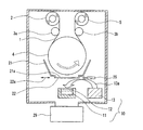
図1は、本実施例において使用した、真空蒸着法を用いて負極活物質としてのシリコン薄膜を成膜するための装置を示した断面図である。 FIG. 1 is a cross-sectional view showing an apparatus for forming a silicon thin film as a negative electrode active material using a vacuum deposition method used in this example.
負極集電体としての基材1は、巻き出しロール2から巻き出され、搬送ロール3a、キャンロール(円筒状基材支持装置)4、搬送ロール3bで順に搬送されて巻き取りロール5に巻き取られる。
The
キャンロール4の下部には蒸着ユニット10が配置されている。蒸着ユニット10は、蒸着ソース(本例ではシリコン)11と、蒸着ソース11を保持するるつぼ12と、電子ビーム13aを発する電子ビーム発生装置13とを備える。電子ビーム発生装置13からの電子ビーム13aは、図示しない偏向ヨークで偏向されて蒸着ソース11を照射して、蒸着ソース11を加熱し蒸発させる。
A
キャンロール4と蒸着ユニット10との間には、開口21aを有する遮蔽板21と、矢印22aの方向に移動して開口21aを開閉するシャッター22とが設けられている。
Between the can roll 4 and the
遮蔽板21とキャンロール4との間であって、開口21aよりも基材1の移動方向の下流側の位置に、被蒸着領域に向けてガス導入ノズル25が配置されている。
A
以上の装置は、真空槽20内に収納される。真空槽20の内部は真空排気装置29により所定の真空度に維持されている。
The above apparatus is accommodated in the
このような装置を用いて、蒸着ソース11としてシリコン約100gをるつぼ12に載せ、電子ビーム発生装置13からの電子ビーム13aを照射して加熱してシリコンを蒸発させた。蒸着ソース11から生成された蒸発粒子は、開口21aを通過して、キャンロール4上を走行している基材(銅箔)1上に堆積してシリコン薄膜を形成した。このようにして、基材1を走行させながら、基材1上に厚さ10μmのシリコン薄膜を連続的に成膜した。
Using such an apparatus, about 100 g of silicon as the
このとき、実施例1〜3、比較例1,2では、ガス導入ノズル25からArガスを8.45×10⁻²Pa・m3/s導入しながら成膜した。ガス導入ノズル25は、基材1の走行方向から見て開口21a内の下流側の端部近傍にのみArガスを供給する。従って、基材1上の特定の地点に着目すると、その地点に形成されるシリコン薄膜の成膜期間のうち、終了側のある期間のみArガスが導入されながら成膜されることになる。実施例1〜3、比較例1,2では、基材1の被成膜面の表面粗さRaを変えて成膜した。一方、比較例3では、Arガスを導入しない以外は実施例2と同様にして成膜した。
At this time, in Examples 1 to 3 and Comparative Examples 1 and 2, the film was formed while introducing Ar gas from the
図2、図4は実施例2の、図3は比較例3の、負極活物質の厚さ方向に沿った断面のSEM写真を模式的に表したものである。図2〜図4において、1は負極集電体としての銅箔(基材)、30は負極活物質としてのシリコン薄膜を構成するシリコン粒子(結晶粒子)である。図2〜図4に示されているように、シリコン粒子30は、厚さ方向(図2〜図4の紙面の上下方向)を長手方向とする柱状構造を有している。しかも、シリコン粒子30の径は、厚さ方向において一定ではない。即ち、図2及び図4(実施例2)では、シリコン粒子30の径は、負極集電体1の表面から徐々に増大し、厚さ方向の略中央近傍にて最大となり、シリコン薄膜の表面に近づくにしたがって小さくなる。これに対して、図3(比較例3)では、シリコン粒子30の径は、負極集電体1の表面から徐々に増大し、シリコン薄膜の表面近傍で最大となる。
2 and 4 schematically show SEM photographs of the cross section along the thickness direction of the negative electrode active material in Example 2 and FIG. 3 in Comparative Example 3. FIG. 2 to 4,
本発明では、厚さ方向におけるシリコン粒子30の径(即ち、シリコン密度)の変化に着目し、厚さ方向においてその径(即ち、密度)が最大となる位置がエネルギーデバイスのサイクル特性に影響を及ぼすことを見出した。
In the present invention, focusing on the change of the diameter (ie, silicon density) of the
即ち、本発明は、図2及び図3に示されているように、厚さ方向においてシリコン密度が最大となる位置の負極集電体1の表面からの距離をh、負極活物質薄膜の厚さをdとしたとき、比h/dに着目する。
That is, according to the present invention, as shown in FIGS. 2 and 3, the distance from the surface of the negative electrode
ここで、距離hは、以下のようにして決定される。即ち、少なくとも10個のシリコン粒子30を含む厚さ方向に沿った断面のSEM写真において、負極集電体1の表面に垂直な方向に、負極集電体1の表面からシリコン薄膜の表面までを100分割する。100個に分割された負極集電体1の表面と平行な個々の領域においてシリコン密度が最大となる領域を決定し、その領域の厚さ方向の中央位置の負極集電体1の表面からの距離を求める。これを、撮影位置が異なる少なくとも10枚のSEM写真について行い、それらから得られる距離の平均値を距離hとする。ここで、シリコン密度とは、SEM写真における前記各領域に対する、シリコン粒子間の空隙を除いたシリコンの存在割合を意味する。
Here, the distance h is determined as follows. That is, in the SEM photograph of the cross section along the thickness direction including at least 10
また、負極活物質薄膜の厚さdは、以下のようにして決定される。即ち、厚さ方向に沿った断面のSEM写真中の特定のシリコン粒子30に着目し、このシリコン粒子30のうち、負極集電体1の表面に対して垂直な方向において負極集電体1の表面から最も離れた箇所の、負極集電体1の表面からの距離をこのシリコン粒子30の高さとする。少なくとも20個のシリコン粒子について同様に高さを求め、その平均値を負極活物質薄膜の厚さdとする。
Moreover, the thickness d of the negative electrode active material thin film is determined as follows. That is, paying attention to the
更に、本発明は、図4に示されているように、厚さ方向においてシリコン密度が最大となる位置での、負極集電体1の表面と平行な方向におけるシリコン粒子30の径をL1、厚さ方向においてシリコン密度が最大となる位置と負極活物質薄膜の表面との距離をL2としたとき、比L2/L1に着目する。
Furthermore, as shown in FIG. 4, the present invention sets the diameters of the
ここで、比L2/L1は以下のようにして決定される。即ち、少なくとも10個のシリコン粒子30を含む厚さ方向に沿った断面のSEM写真において、負極集電体1の表面に垂直な方向に、負極集電体1の表面からシリコン薄膜の表面までを100分割する。100個に分割された負極集電体1の表面と平行な個々の領域においてシリコン密度が最大となる領域を決定する。その領域の厚さ方向の中央位置を通り負極集電体1の表面と平行な直線に沿ったシリコン粒子30の径L1’を求める。また、この直線と、これより最も離れた位置にあるシリコン粒子30の頂点との距離L2’を求める。これより比L2’/L1’を求める。少なくとも20個のシリコン粒子30について同様に比L2’/L1’を求め、その平均値を比L2/L1とする。
Here, the ratio L2 / L1 is determined as follows. That is, in the SEM photograph of the cross section along the thickness direction including at least 10
実施例1〜3,比較例1〜3で形成したリチウムイオン二次電池に対し、0.2Cの充放電速度で、50サイクル後及び200サイクル後の充放電サイクル試験を行った。サイクル試験後の電池容量維持率を表1に示す(順に「50サイクル後」及び「200サイクル後」と表示)。併せて、比h/d及び比L2/L1を示す。 The lithium ion secondary batteries formed in Examples 1 to 3 and Comparative Examples 1 to 3 were subjected to charge / discharge cycle tests after 50 cycles and 200 cycles at a charge / discharge rate of 0.2C. The battery capacity retention rate after the cycle test is shown in Table 1 (in the order “after 50 cycles” and “after 200 cycles”). In addition, the ratio h / d and the ratio L2 / L1 are shown.

負極集電体1の被成膜面の表面粗さRaが0.1μmを超える比較例2では、h/d>0.8且つL2/L1<0.5である。即ち、シリコン粒子は、負極活物質薄膜の表面近傍に最大径部を有する略逆円錐形状を有していた。このような比較例2では、良好なサイクル特性は得られなかった。
In Comparative Example 2 where the surface roughness Ra of the deposition surface of the negative electrode
負極集電体1の被成膜面の表面粗さRaが0.01μm未満の比較例1では、h/d>0.8且つL2/L1<0.5である。即ち、シリコン粒子は、負極活物質薄膜の表面近傍に最大径部を有する略逆円錐形状を有していた。また、負極集電体1の近傍でもシリコン粒子が比較的高密度で成長していた。これらに加えて、負極集電体1の被成膜面が平滑であることにより、負極集電体1とシリコン薄膜との剥離が生じやすく、そのため50サイクル後のサイクル特性が劣っていた。また、200サイクルの充放電を繰り返す過程で負極集電体1とシリコン薄膜との界面で剥離を生じた。これは、シリコン粒子の膨張/収縮による応力に界面が耐えられなかったためであると考えられる。
In Comparative Example 1 where the surface roughness Ra of the deposition surface of the negative electrode
更に、シリコン薄膜の成膜中にArガス導入を行わなかった比較例3では、h/d>0.8且つL2/L1<0.5である。即ち、シリコン粒子は、負極活物質薄膜の表面近傍に最大径部を有する略逆円錐形状を有していた。このような比較例3では、良好なサイクル特性は得られなかった。 Furthermore, in Comparative Example 3 where Ar gas was not introduced during the formation of the silicon thin film, h / d> 0.8 and L2 / L1 <0.5. That is, the silicon particles had a substantially inverted conical shape having a maximum diameter portion near the surface of the negative electrode active material thin film. In such Comparative Example 3, good cycle characteristics could not be obtained.
なお、実施例1〜3のそれぞれのシリコン薄膜は、X線回折測定(CuKα、40kV)でいずれも顕著なシリコン結晶に相当するピークが検出されず、アモルファスまたは微結晶であることが推定できた。 In addition, each silicon thin film of Examples 1-3 did not detect a peak corresponding to a remarkable silicon crystal by X-ray diffraction measurement (CuKα, 40 kV), and could be estimated to be amorphous or microcrystalline. .
(実施例4〜8,比較例4)
負極集電体1として被成膜面の表面粗さRaが0.125μmの銅箔を用い、成膜中に供給する不活性ガスの種類を変える以外は実施例2と同様にしてシリコン薄膜を成膜し、リチウムイオン二次電池を作製した(実施例4〜8)。また、不活性ガスに代えて酸素ガスを供給しながら成膜する以外は実施例2と同様にしてシリコン薄膜を成膜し、リチウムイオン二次電池を作製した(比較例4)。
(Examples 4-8, Comparative Example 4)
A silicon thin film is formed in the same manner as in Example 2 except that a copper foil having a surface roughness Ra of 0.125 μm is used as the negative electrode
実施例4〜8,比較例4で形成したリチウムイオン二次電池に対し、0.2Cの充放電速度で、50サイクル後及び200サイクル後の充放電サイクル試験を行った。サイクル試験後の電池容量維持率、比h/d、比L2/L1を表2に示す。 The lithium ion secondary batteries formed in Examples 4 to 8 and Comparative Example 4 were subjected to charge / discharge cycle tests after 50 cycles and 200 cycles at a charge / discharge rate of 0.2C. Table 2 shows the battery capacity retention rate, the ratio h / d, and the ratio L2 / L1 after the cycle test.
シリコン粒子が、負極活物質薄膜の表面近傍に最大径部を有する略逆円錐形状を有していた。また、シリコン薄膜が成長せず多くは酸化シリコンのアモルファスもしくは微結晶となったと推定され、サイクル特性が極めて悪い。
The silicon particles had a substantially inverted conical shape having a maximum diameter portion near the surface of the negative electrode active material thin film. Further, it is presumed that the silicon thin film did not grow and most of them became amorphous or microcrystalline silicon oxide, and the cycle characteristics were extremely poor.
これに対し実施例4〜8のように、導入ガスとして不活性ガスを用いた場合においては良好なサイクル特性を得ることができた。 On the other hand, when the inert gas was used as the introduced gas as in Examples 4 to 8, good cycle characteristics could be obtained.
実施例4〜8では不活性ガスとして、N2、He、Ne、Ar、Xeを用いたが、本発明は導入ガスとしてSiと反応しない不活性ガスであればよく、実施例4〜8で用いたガスに限られるものではない。 In Examples 4 to 8, N 2 , He, Ne, Ar, and Xe were used as the inert gas. However, the present invention may be any inert gas that does not react with Si as the introduced gas. It is not limited to the gas used.
なお、実施例4〜8のそれぞれのシリコン薄膜は、X線回折測定(CuKα、40kV)でいずれも顕著なシリコン結晶に相当するピークが検出されず、アモルファスまたは微結晶であることが推定できた。 In each of the silicon thin films of Examples 4 to 8, no peak corresponding to a remarkable silicon crystal was detected by X-ray diffraction measurement (CuKα, 40 kV), and it was estimated that the silicon thin film was amorphous or microcrystalline. .
(実施例9〜12,比較例5)
負極の製造方法を以下のように変更する以外は実施例1と同様にしてリチウムイオン二次電池を作製した。
(Examples 9 to 12, Comparative Example 5)
A lithium ion secondary battery was produced in the same manner as in Example 1 except that the method for producing the negative electrode was changed as follows.
図5は、本実施例において使用した、真空蒸着法を用いて負極活物質としてのシリコン薄膜を成膜するための装置を示した断面図である。 FIG. 5 is a cross-sectional view showing an apparatus for forming a silicon thin film as a negative electrode active material using a vacuum vapor deposition method used in this example.
図5の装置はガス導入ノズル25の配置において図1に示した装置と異なる。即ち、図5の装置では、ガス導入ノズル25は、遮蔽板21と蒸着ユニット10との間の空間に、開口21aに向かってガスを供給できるように配置されている。これ以外は図1に示した装置と同様であり、図1と同じ構成要素には同じ符号を付してそれらについての詳細な説明を省略する。
The apparatus shown in FIG. 5 differs from the apparatus shown in FIG. That is, in the apparatus of FIG. 5, the
このような装置を用いて、蒸着ソース11としてシリコン約100gをるつぼ12に載せ、電子ビーム発生装置13からの電子ビーム13aを照射して加熱してシリコンを蒸発させた。蒸着ソース11から生成された蒸発粒子は、開口21aを通過して、キャンロール4上の基材1上に堆積してシリコン薄膜を形成した。
Using such an apparatus, about 100 g of silicon as the
負極集電体(基材)1として厚さ30μm、被成膜面のRaが0.125μmの銅箔を用いた。シャッター22を時間T=600秒だけ開放し、このシャッター開放時間Tの間は基材1の搬送を停止して、基材1上に厚さ10μmのシリコン薄膜を成膜した。時間Tが経過後、シャッター22を閉じ、基材1を開口21aの開口長とほぼ同じ長さだけ巻き出しロール2から巻き取りロール5に搬送した。その後、再度シャッター22を時間T=600秒だけ開放し、基材1上に厚さ10μmのシリコン薄膜を成膜した。この動作を繰り返し、基材1を間欠的に搬送して、基材1上にシリコン薄膜を成膜した。
As the negative electrode current collector (base material) 1, a copper foil having a thickness of 30 μm and an Ra of the film formation surface of 0.125 μm was used. The
更に、シャッター22を解放した時刻を0として、時刻t秒から成膜終了(t=600秒)までの間は、ガス導入ノズル25からArガスを8.45×10⁻²Pa・m3/s導入し続けた。
Further, the time when the
以上の方法において、Arガスの導入開始時刻tを変化させてシリコン薄膜を成膜した(実施例9〜12,比較例5)。 In the above method, the silicon thin film was formed by changing the Ar gas introduction start time t (Examples 9 to 12, Comparative Example 5).
実施例9〜12,比較例5で形成したリチウムイオン二次電池に対し、0.2Cの充放電速度で、50サイクル後及び200サイクル後の充放電サイクル試験を行った。サイクル試験後の電池容量維持率、比h/d、比L2/L1を表3に示す。 The lithium ion secondary batteries formed in Examples 9 to 12 and Comparative Example 5 were subjected to charge / discharge cycle tests after 50 cycles and 200 cycles at a charge / discharge rate of 0.2C. Table 3 shows the battery capacity retention rate, the ratio h / d, and the ratio L2 / L1 after the cycle test.
なお、実施例9〜12のそれぞれのシリコン薄膜は、X線回折測定(CuKα、40kV)でいずれも顕著なシリコン結晶に相当するピークが検出されず、アモルファスまたは微結晶であることが推定できた。 In each of the silicon thin films of Examples 9 to 12, no peak corresponding to a remarkable silicon crystal was detected by X-ray diffraction measurement (CuKα, 40 kV), and it was estimated that the silicon thin film was amorphous or microcrystalline. .
(実施例13〜15,比較例6)
実施例1のセパレータおよび電解質に代えて固体電解質を用い、負極集電体1の被成膜面の表面粗さRaを種々に変化させる以外は実施例1と同様にしてリチウムイオン二次電池を作製した(実施例13〜15)。固体電解質は、リン酸リチウムを抵抗加熱装置を用いて500℃に加熱し、真空蒸着法を用いて形成した厚さ1μmの薄膜を用いた。また、負極活物質薄膜の形成時にArガスの導入を行わない以外は実施例14と同様にしてリチウムイオン二次電池を作製した(比較例6)。
(Examples 13 to 15, Comparative Example 6)
A lithium ion secondary battery was prepared in the same manner as in Example 1 except that a solid electrolyte was used in place of the separator and electrolyte of Example 1 and the surface roughness Ra of the deposition surface of the negative electrode
実施例13〜15,比較例6で形成したリチウムイオン二次電池に対し、0.2Cの充放電速度で、50サイクル後及び200サイクル後の充放電サイクル試験を行った。サイクル試験後の電池容量維持率、比h/d、比L2/L1を表4に示す。 The lithium ion secondary batteries formed in Examples 13 to 15 and Comparative Example 6 were subjected to charge / discharge cycle tests after 50 cycles and 200 cycles at a charge / discharge rate of 0.2C. Table 4 shows the battery capacity retention rate, the ratio h / d, and the ratio L2 / L1 after the cycle test.
一方、シリコン薄膜の成膜時に不活性ガスの導入を行わない比較例6は、0<h/d≦0.8及びL2/L1≧0.5のいずれをも満足せず、サイクル特性が劣っていた。 On the other hand, Comparative Example 6 in which no inert gas was introduced during the formation of the silicon thin film did not satisfy both 0 <h / d ≦ 0.8 and L2 / L1 ≧ 0.5, and the cycle characteristics were inferior. It was.
本発明のエネルギーデバイスの利用分野は特に限定されないが、例えば薄型、軽量の小型携帯機器の2次電池として利用することができる。 The field of application of the energy device of the present invention is not particularly limited, but it can be used as a secondary battery for a thin, lightweight, small portable device, for example.
1 基材
2 巻き出しロール
3a,3b 搬送ロール
4 キャンロール
5 巻き取りロール
10 蒸着ユニット
11 蒸着ソース
12 るつぼ
13 電子ビーム発生装置
13a 電子ビーム
20 真空槽
21 遮蔽板
21a 開口
22 シャッター
22a シャッター移動方向
25 ガス導入ノズル
29 真空排気装置
30 シリコン粒子
DESCRIPTION OF
Claims (2)
前記負極活物質薄膜に含まれる全ての前記シリコンの柱状粒子は、その径が前記負極集電体の表面から遠ざかるにしたがって徐々に増大し、最大となったのち、シリコン薄膜の表面に近づくにしたがって小さくなる略樽型であり、
厚さ方向においてシリコン密度が最大となる位置の前記負極集電体の表面からの距離をh、前記負極活物質薄膜の厚さをdとしたとき、0<h/d≦0.8であり、
厚さ方向においてシリコン密度が最大となる位置での、前記負極集電体の表面と平行な方向における前記シリコンの柱状粒子の径をL1、厚さ方向においてシリコン密度が最大となる位置と前記負極活物質薄膜の表面との距離をL2としたとき、L2/L1≧0.5であることを特徴とするエネルギーデバイス。 An energy device comprising a negative electrode current collector and a negative electrode active material thin film containing columnar particles of silicon formed thereon,
All of the silicon columnar particles contained in the negative electrode active material thin film gradually increase in diameter as they move away from the surface of the negative electrode current collector, and after reaching the maximum, approach the surface of the silicon thin film. It is a roughly barrel type that gets smaller,
When the distance from the surface of the negative electrode current collector at the position where the silicon density is maximum in the thickness direction is h and the thickness of the negative electrode active material thin film is d, 0 <h / d ≦ 0.8. ,
The diameter of the silicon columnar particles in the direction parallel to the surface of the negative electrode current collector at the position where the silicon density is maximum in the thickness direction is L1, and the position where the silicon density is maximum in the thickness direction and the negative electrode An energy device, wherein L2 / L1 ≧ 0.5 when the distance from the surface of the active material thin film is L2.
Priority Applications (1)
| Application Number | Priority Date | Filing Date | Title |
|---|---|---|---|
| JP2004016101A JP4526825B2 (en) | 2004-01-23 | 2004-01-23 | Energy device |
Applications Claiming Priority (1)
| Application Number | Priority Date | Filing Date | Title |
|---|---|---|---|
| JP2004016101A JP4526825B2 (en) | 2004-01-23 | 2004-01-23 | Energy device |
Publications (3)
| Publication Number | Publication Date |
|---|---|
| JP2005209533A JP2005209533A (en) | 2005-08-04 |
| JP2005209533A5 JP2005209533A5 (en) | 2007-01-25 |
| JP4526825B2 true JP4526825B2 (en) | 2010-08-18 |
Family
ID=34901359
Family Applications (1)
| Application Number | Title | Priority Date | Filing Date |
|---|---|---|---|
| JP2004016101A Expired - Lifetime JP4526825B2 (en) | 2004-01-23 | 2004-01-23 | Energy device |
Country Status (1)
| Country | Link |
|---|---|
| JP (1) | JP4526825B2 (en) |
Families Citing this family (15)
| Publication number | Priority date | Publication date | Assignee | Title |
|---|---|---|---|---|
| WO2007046322A1 (en) * | 2005-10-21 | 2007-04-26 | Matsushita Electric Industrial Co., Ltd. | Battery |
| JP2007184252A (en) * | 2005-12-05 | 2007-07-19 | Mitsubishi Chemicals Corp | Method of manufacturing electrode material for nonaqueous electrolyte secondary battery, electrode for nonaqueous electrolyte secondary battery and its manufacturing method, method of manufacturing electrode collector for nonaqueous electrolyte secondary battery, and nonaqueous secondary battery |
| JP5130738B2 (en) * | 2006-02-16 | 2013-01-30 | パナソニック株式会社 | Nonaqueous electrolyte secondary battery |
| JP5130737B2 (en) * | 2006-02-16 | 2013-01-30 | パナソニック株式会社 | Nonaqueous electrolyte secondary battery |
| JP2007280926A (en) * | 2006-03-14 | 2007-10-25 | Matsushita Electric Ind Co Ltd | Manufacturing method of negative electrode for non-aqueous electrolyte secondary battery, and non-aqueous electrolyte secondary battery using it |
| JP5092280B2 (en) * | 2006-05-24 | 2012-12-05 | ソニー株式会社 | Secondary battery electrode, method for manufacturing the same, and secondary battery |
| JP5210162B2 (en) * | 2006-08-25 | 2013-06-12 | パナソニック株式会社 | Anode for non-aqueous electrolyte secondary battery, method for producing the same, and non-aqueous electrolyte secondary battery |
| US8734997B2 (en) | 2006-10-10 | 2014-05-27 | Panasonic Corporation | Negative electrode for nonaqueous electrolyte secondary battery |
| CN101449408B (en) * | 2006-10-19 | 2011-04-13 | 松下电器产业株式会社 | Negative electrode for lithium secondary battery and lithium secondary battery containing the same |
| US7851089B2 (en) | 2006-10-26 | 2010-12-14 | Panasonic Corporation | Electrode plate for battery and lithium secondary battery including the same |
| JP2010212213A (en) * | 2009-03-12 | 2010-09-24 | Nissan Motor Co Ltd | Electrode for secondary battery |
| KR101941142B1 (en) * | 2010-06-01 | 2019-01-22 | 가부시키가이샤 한도오따이 에네루기 켄큐쇼 | Energy storage device and manufacturing method thereof |
| KR20130024769A (en) | 2011-08-30 | 2013-03-08 | 가부시키가이샤 한도오따이 에네루기 켄큐쇼 | Power storage device |
| JPWO2021241130A1 (en) * | 2020-05-29 | 2021-12-02 | ||
| CN117378057A (en) * | 2021-05-17 | 2024-01-09 | 松下知识产权经营株式会社 | Battery and method for manufacturing battery |
Citations (1)
| Publication number | Priority date | Publication date | Assignee | Title |
|---|---|---|---|---|
| JP2002313319A (en) * | 2001-04-09 | 2002-10-25 | Sanyo Electric Co Ltd | Electrode for lithium secondary battery and lithium secondary battery |
-
2004
- 2004-01-23 JP JP2004016101A patent/JP4526825B2/en not_active Expired - Lifetime
Patent Citations (1)
| Publication number | Priority date | Publication date | Assignee | Title |
|---|---|---|---|---|
| JP2002313319A (en) * | 2001-04-09 | 2002-10-25 | Sanyo Electric Co Ltd | Electrode for lithium secondary battery and lithium secondary battery |
Also Published As
| Publication number | Publication date |
|---|---|
| JP2005209533A (en) | 2005-08-04 |
Similar Documents
| Publication | Publication Date | Title |
|---|---|---|
| JP4642835B2 (en) | Current collector for electrode | |
| JP4526825B2 (en) | Energy device | |
| US20100143583A1 (en) | Energy device and method for producing the same | |
| JP4994634B2 (en) | Negative electrode for lithium ion secondary battery, method for producing the same, and lithium ion secondary battery using the same | |
| JP4036889B2 (en) | battery | |
| US8888870B2 (en) | Lithium secondary battery | |
| JP4351732B2 (en) | ELECTRODE FOR LITHIUM SECONDARY BATTERY AND LITHIUM SECONDARY BATTERY HAVING THE SAME | |
| JP3913490B2 (en) | Method for producing electrode for lithium secondary battery | |
| JP4602478B2 (en) | Lithium secondary battery manufacturing method and lithium secondary battery | |
| JP4850405B2 (en) | Lithium ion secondary battery and manufacturing method thereof | |
| US20100075217A1 (en) | Lithium ion secondary battery and method for producing the same | |
| JP2005196970A (en) | Negative pole for nonaqueous electrolyte secondary battery, its manufacturing method and nonaqueous electrolyte secondary battery using it | |
| JPWO2007094311A1 (en) | Non-aqueous electrolyte secondary battery electrode, method for producing the same, and non-aqueous electrolyte secondary battery equipped with non-aqueous electrolyte secondary battery electrode | |
| JP4598150B2 (en) | Method for producing electrode for non-aqueous electrolyte secondary battery | |
| JP4045270B2 (en) | Energy device and manufacturing method thereof | |
| JP2008293970A (en) | Electrode for electrochemical element and method of manufacturing the same | |
| JP2007122992A (en) | Negative electrode for lithium secondary battery and manufacturing method of lithium secondary battery | |
| JP2007095363A (en) | Electrode material for battery and manufacturing method of electrode material for battery | |
| JP2005183364A5 (en) | ||
| JP2008047303A (en) | Nonaqueous electrolyte secondary battery | |
| CN113994503A (en) | Protective interface for lithium ion battery anode | |
| JP4748970B2 (en) | Energy device and manufacturing method thereof | |
| JP2007207663A (en) | Method of manufacturing negative electrode of lithium-ion secondary battery, and lithium-ion secondary battery including negative electrode obtained using its method | |
| JP5089276B2 (en) | Energy device and manufacturing method thereof | |
| JP2007172991A (en) | Negative electrode for lithium secondary battery, method for manufacturing same, and lithium secondary battery |
Legal Events
| Date | Code | Title | Description |
|---|---|---|---|
| A521 | Request for written amendment filed |
Free format text: JAPANESE INTERMEDIATE CODE: A523 Effective date: 20061205 |
|
| A621 | Written request for application examination |
Free format text: JAPANESE INTERMEDIATE CODE: A621 Effective date: 20061205 |
|
| A977 | Report on retrieval |
Free format text: JAPANESE INTERMEDIATE CODE: A971007 Effective date: 20091120 |
|
| A131 | Notification of reasons for refusal |
Free format text: JAPANESE INTERMEDIATE CODE: A131 Effective date: 20100304 |
|
| A521 | Request for written amendment filed |
Free format text: JAPANESE INTERMEDIATE CODE: A523 Effective date: 20100415 |
|
| TRDD | Decision of grant or rejection written | ||
| A01 | Written decision to grant a patent or to grant a registration (utility model) |
Free format text: JAPANESE INTERMEDIATE CODE: A01 Effective date: 20100511 |
|
| A01 | Written decision to grant a patent or to grant a registration (utility model) |
Free format text: JAPANESE INTERMEDIATE CODE: A01 |
|
| A61 | First payment of annual fees (during grant procedure) |
Free format text: JAPANESE INTERMEDIATE CODE: A61 Effective date: 20100602 |
|
| FPAY | Renewal fee payment (event date is renewal date of database) |
Free format text: PAYMENT UNTIL: 20130611 Year of fee payment: 3 |
|
| R150 | Certificate of patent or registration of utility model |
Ref document number: 4526825 Country of ref document: JP Free format text: JAPANESE INTERMEDIATE CODE: R150 Free format text: JAPANESE INTERMEDIATE CODE: R150 |
|
| EXPY | Cancellation because of completion of term |