JP4524924B2 - Discharge lamp lighting device - Google Patents
Discharge lamp lighting device Download PDFInfo
- Publication number
- JP4524924B2 JP4524924B2 JP2001005710A JP2001005710A JP4524924B2 JP 4524924 B2 JP4524924 B2 JP 4524924B2 JP 2001005710 A JP2001005710 A JP 2001005710A JP 2001005710 A JP2001005710 A JP 2001005710A JP 4524924 B2 JP4524924 B2 JP 4524924B2
- Authority
- JP
- Japan
- Prior art keywords
- power
- input voltage
- circuit
- discharge lamp
- input
- Prior art date
- Legal status (The legal status is an assumption and is not a legal conclusion. Google has not performed a legal analysis and makes no representation as to the accuracy of the status listed.)
- Expired - Fee Related
Links
Images


Landscapes
- Circuit Arrangements For Discharge Lamps (AREA)
Description
【0001】
【発明の属する技術分野】
本発明は、メタルハライドランプ等の放電灯を負荷とする放電灯点灯装置に関するものである。
【0002】
【従来の技術】
近年、自動車の前照灯用の放電灯としてメタルハライドランプが用いられることが多い。メタルハライドランプ(以下、ランプと略称する)を前照灯に用いる場合、その用途の性格上、ランプの起動後に光束が安定するまでの時間を短縮する必要があり、そのためにランプに過大な電力を供給しなければならない。そして、光束が安定した後は電源(車載用のバッテリ)の電源電圧変動に対してランプの定格電力値を越えないように定電力制御が行われている。
【0003】
図11は従来の放電灯点灯装置の一例を示すブロック図である。この従来装置は、例えば12V系や24V系などのバッテリからなる直流電源Eと、直流電源Eからの入力電圧を所望の直流電圧に変換するDC/DCコンバータ1と、DC/DCコンバータ1の直流電圧を低周波(例えば、数100Hz)の交流電圧に変換してメタルハライドランプからなる放電灯4に供給するフルブリッジ型のインバータ回路2と、放電灯4への電力供給開始時に放電灯4に高電圧を印可することで絶縁破壊を引き起こして放電灯4を始動するイグナイタ回路3と、DC/DCコンバータ1の出力電圧及び出力電流の検出値に応じて放電灯4に適切且つ略一定の電力を供給するようにDC/DCコンバータ1を制御する制御回路50とを備えており、例えば車載用前照灯の点灯装置として用いられる。DC/DCコンバータ1は、例えばスイッチング素子やインダクタ、ダイオード並びに平滑コンデンサ等を有する従来周知の昇圧チョッパ回路からなる。
【0004】
制御回路50は、DC/DCコンバータ1の出力電圧を分圧抵抗R1,R2で分圧した電圧からDC/DCコンバータ1の出力電圧、すなわち放電灯4に供給されるランプ電圧を検出するとともに、DC/DCコンバータ1の出力ラインに接続された電流検出用抵抗R3に発生する電圧からDC/DCコンバータ1の出力電流、すなわち放電灯4に流れるランプ電流を検出し、これらの検出値から放電灯4に供給される電力、すなわちランプ電力を演算する電力演算部51と、所定の電力設定値と電力演算部51で求めたランプ電力を誤差増幅する誤差増幅部52と、誤差増幅部52の出力信号に応じて発振周波数を可変する発振回路53と、発振回路53が出力する高周波発振信号に基づいてDC/DCコンバータ1が具備するスイッチング素子(図示せず)をオンオフ駆動する駆動回路54とを具備し、放電灯4に供給する電力が略一定となるようにDC/DCコンバータ1のスイッチング素子の駆動周波数を可変制御する。但し、制御回路50は、誤差増幅部52の出力信号と高周波発振信号を比較し、DC/DCコンバータ1のスイッチング素子のオンデューティ比を決定する従来周知のPWM制御を行ってもよい。
【0005】
ところで、放電灯点灯装置の小型化によって回路部品が発する熱の放熱面積も小さくなっており、回路部品における熱損失(以下、「回路損失」という)が同じであっても回路部品の温度上昇が大きくなっている。また、放電灯点灯装置の小型化により設置場所の自由度が高まっているため、ランプの近傍に放電灯点灯装置を設置することが増えている。その結果、ランプの発する熱によってさらに回路部品の温度が上昇するため、熱による回路部品の特性劣化や破壊を防ぐために回路部品の温度上昇を抑えることが要求されている。
【0006】
そこで、バッテリの電圧変動に伴う回路損失の増加を防止するため、損失の少ない回路部品を使用して装置全体の回路損失を低減したり、あるいは許容損失(最大許容損失)の大きい回路部品の使用や放熱性の高い構造を採用することで回路損失に対する許容量を増大するなどの対策が採られている。
【0007】
【発明が解決しようとする課題】
ところが、上述のような従来の対策では、特性の良い(損失の少ない)回路部品や許容損失の大きな回路部品を使用しなければならず、放電灯点灯装置のコスト上昇を招いてしまうという問題がある。また、小型化と放熱性向上を同時に達成する構造も同様にコストが高くなってしまう。しかも、ランプ近傍に設置される場合、上述のような対策を講じても回路部品の特性劣化や破壊を防ぐことができない虞がある。
【0008】
本発明は上記問題に鑑みて為されたものであり、その目的とするところは、小型化やランプ近傍への設置を可能としながら回路部品の温度上昇を抑えて特性劣化や破壊等の不具合の発生を防ぐことができる放電灯点灯装置を提供することにある。
【0009】
【課題を解決するための手段】
請求項1の発明は、上記目的を達成するために、直流電源と、直流電源の直流電力を電力変換して放電灯に供給する電力変換手段と、この電力変換手段を制御して放電灯に略一定電力を供給する制御手段とを備えた放電灯点灯装置において、直流電源からの入力電力を検出する入力電力検出手段と、放電灯に供給する出力電力を検出する出力電力検出手段とを設け、制御手段は入力電力と出力電力から求まる回路損失が所定値を上回ると当該回路損失に応じて前記略一定電力を低減することを特徴とし、電力変換手段から放電灯に供給する略一定電力を低減することで回路損失を低減し、小型化やランプ近傍への設置を可能としながら回路部品の温度上昇を抑えて特性劣化や破壊等の不具合の発生を防ぐことができる。
【0010】
請求項2の発明は、請求項1の発明において、制御手段は、放電灯の始動後から放電灯が安定点灯して放電灯への供給電力を前記略一定電力に調整するまでの移行期間に、回路損失に応じて出力電力を抑制することを特徴とし、入力電流が最も大きくなる移行期間における入力電流ピークを低下させることができ、その結果、電力変換手段を構成する回路部品に電流容量の小さい部品を使用することができる。
【0011】
請求項3の発明は、請求項1の発明において、電力変換手段への入力電圧を検出する入力電圧検出手段を備え、制御手段は入力電圧検出手段が検出する入力電圧が所定値を下回ると回路損失に応じて前記略一定電力を低減することを特徴とし、最も回路損失が増大する入力電圧低下時に回路部品の温度上昇を抑えることができる。
【0012】
請求項4の発明は、請求項1の発明において、制御手段は、回路損失が所定の制限値を越えないように前記略一定電力を低減することを特徴とし、回路部品の温度上昇を簡単な制御で抑えることができる。
【0013】
請求項5の発明は、請求項1の発明において、電力変換手段への入力電圧を検出する入力電圧検出手段を備え、制御手段は、回路損失が所定の制限値を越えないように電力変換手段を制御するとともに入力電圧検出手段が検出する入力電圧に応じて制限値を可変することを特徴とし、制限値を一定とするよりも広範な入力電圧範囲で回路部品の温度上昇を抑えることができる。
【0014】
請求項6の発明は、請求項1の発明において、電力変換手段への入力電圧を検出する入力電圧検出手段を備え、制御手段は、回路損失が所定の制限値を越えないように電力変換手段を制御するとともに、入力電圧検出手段が検出する入力電圧が所定値を越える場合には制限値を一定とし、入力電圧検出手段が検出する入力電圧が所定値を下回る場合には当該入力電圧に応じて制限値を可変することを特徴とし、入力電圧の変化に対して回路損失の低減を連続的に行うことができ、回路部品の温度上昇をきめ細かく抑えることができる。
【0015】
【発明の実施の形態】
(実施形態1)
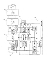
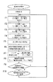
図1に本発明の実施形態1のブロック図を示す。但し、本実施形態の基本回路構成は従来例と共通であるので、共通する構成要素には同一の符号を付して説明を省略する。
【0016】
本実施形態は、車載用のバッテリからなる直流電源Eと、チョッパ回路からなるDC/DCコンバータ1と、フルブリッジ型のインバータ回路2と、イグナイタ回路3と、メタルハライドランプからなる放電灯4とを備え、自動車等の車載用前照灯の点灯装置として用いられる。
【0017】
また、本実施形態の制御回路5は、従来例の制御回路50が具備する電力演算部51、誤差増幅部52、発振回路53、駆動回路54の他に、DC/DCコンバータ1の入力電圧を分圧抵抗R4,R5で分圧した電圧からDC/DCコンバータ1の入力電圧を検出するとともに、DC/DCコンバータ1の入力ラインに接続された入力電流検出回路6によりDC/DCコンバータ1の入力電流を検出し、これらの検出値からDC/DCコンバータ1の入力電力を演算する入力電力演算部55と、電力演算部51で求めた出力電力と入力電力演算部55で求めた入力電力から回路損失を算出する回路損失算出回路56とを備え、誤差増幅部52の出力信号だけでなく、回路損失算出回路56の出力信号に応じて発振回路53の発振周波数を可変するように構成される。なお、入力電流検出回路6には入力ラインに接続された電流検出用抵抗に発生する電圧を検出する構成を採用しても良いし、あるいはDC/DCコンバータ1がフライバック型の場合にはスイッチング素子に流れる電流等から算出する構成を採用しても良い。
【0018】
而して、制御回路5は、従来例における制御回路50と同様に、電力演算部51で求めた出力電力に応じてDC/DCコンバータ1のスイッチング素子の駆動周波数を可変することにより放電灯4に供給する電力を略一定に制御する。但し、車載用前照灯に利用する場合には放電灯4の始動直後から一定量以上の光束を得る必要があるため、制御回路5では始動後から放電灯4が安定点灯して放電灯4への供給電力を略一定に調整するまでの移行期間に放電灯4の定格電力以上の電力を放電灯4に供給する制御を行っており、移行期間が経過して放電灯4が安定点灯し一定量以上の光束が得られるようになれば、放電灯4の定格電力を越えないようにDC/DCコンバータ1の出力電力を略一定に制御している。
【0019】
上述の説明は回路損失算出回路56で算出される回路損失が所定の制限値を越えない場合の制御動作(以下、「定常制御動作」という)であって、回路損失が上記制限値を越える場合、制御回路5では誤差増幅部52の出力信号に対して回路損失算出回路56の出力信号を優先し、回路損失算出回路56の出力信号に応じて発振回路53の発振周波数を可変することでDC/DCコンバータ1の出力電力を抑制する制御動作(以下、「出力抑制制御動作」という)を行う。そして、出力電力の抑制によって回路損失が制限値以下に低減すれば、制御回路5は再度定常制御動作を行う。
【0020】
上述のように本実施形態では、直流電源Eからの入力電力を検出するとともに、放電灯4に供給する出力電力を検出し、これらの入力電力と出力電力から求まる回路損失に応じて出力電力を抑制するようにDC/DCコンバータ1を制御する制御回路5を備えているので、出力電力を抑制することで回路損失を低減し、放電灯点灯装置の小型化やランプ近傍への設置を可能としながら回路部品の温度上昇を抑えて特性劣化や破壊等の不具合の発生を防ぐことができる。
【0021】
(実施形態2)
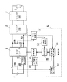
図2に本発明の実施形態2のブロック図を示す。但し、本実施形態の基本回路構成は実施形態1と共通であるので、共通する構成要素には同一の符号を付して説明を省略する。本実施形態は、放電灯4の始動から出力電力を略一定に制御する定電力制御に至るまでの移行期間に回路損失の制限を行う点に特徴がある。すなわち、車載用前照灯を点灯する点灯装置においては、既に説明したように放電灯4の始動後に光束が安定するまでの時間(移行期間)を短縮するためにこの移行期間に過大な電力を放電灯4に供給しており、移行期間には回路損失も安定点灯時の倍以上に増大することになる。本実施形態は、かかる事情に鑑みて移行期間における回路損失を制限するものである。
【0022】
図2に示すように、DC/DCコンバータ1の入力側にはDC/DCコンバータ1の入力電圧を検出するとともに検出した入力電圧をA/D変換した入力電圧検出信号を制御回路7に出力する入力電圧検出回路8が接続される。また、DC/DCコンバータ1の入力ラインにはDC/DCコンバータ1の入力電流を検出するとともに検出した入力電流をA/D変換した入力電流検出信号を制御回路7に出力する入力電流検出回路9が接続される。一方、DC/DCコンバータ1の出力側にはDC/DCコンバータ1の出力電圧(すなわち、放電灯4に供給されるランプ電圧)を検出するとともに検出した出力電圧をA/D変換した出力電圧検出信号を制御回路7に出力する出力電圧検出回路10が接続される。また、DC/DCコンバータ1の出力ラインにはDC/DCコンバータ1の出力電流(すなわち、放電灯4に流れるランプ電流)を検出するとともに検出した出力電流をA/D変換した出力電流検出信号を制御回路7に出力する出力電流検出回路11が接続される。
【0023】
また、本実施形態における制御回路7はマイクロコンピュータを主構成要素とし、内蔵のメモリ等に格納されたプログラムを実行することで以下の各部の機能を実現している。出力電力演算部71は出力電圧検出信号と出力電流検出信号からDC/DCコンバータ1の出力電力を演算し、演算した出力電力(出力電力データ)を回路損失算出部76に与える。同じく入力電力演算部75は入力電圧検出信号と入力電流検出信号からDC/DCコンバータ1の入力電力を演算し、演算した入力電力(入力電力データ)を回路損失算出部76に与える。回路損失算出部76では出力電力データと入力電力データから回路損失を算出し、算出した回路損失(回路損失データ)を比較部78に与える。また、回路損失制限値決定部77が入力電圧検出信号に基づき、内蔵のメモリ等に予め格納されている回路損失制限値用のテーブルを参照して回路損失の制限値を決定する。比較部78では回路損失制限値決定部77で決定した回路損失の制限値と回路損失算出部76で算出した回路損失とを比較し、回路損失が制限値を越える場合に点灯制御回路79に対して点灯制御停止命令を与え、回路損失が制限値を越えない場合には点灯制御停止命令を与えない。
【0024】
一方、電力指令値設定部72では、上記移行期間において経時的に変化させる必要がある出力電力の指令値(出力電力指令値)を、内蔵メモリに格納されている出力電力指令値テーブルから随時読み出してランプ電流指令値演算部73に与える。ランプ電流指令値演算部73は出力電力指令値を出力電圧検出信号で示されるランプ電圧で除算することによりランプ電流指令値を演算する。そして、誤差増幅部74では出力電流検出信号で示されるランプ電流をランプ電流指令値から減算した電流誤差値を点灯制御回路79に与える。点灯制御回路79では電流誤差値を小さくするように、すなわち実際のランプ電流をランプ電流指令値に略一致させるようにDC/DCコンバータ1のスイッチング素子(図示せず)を駆動する駆動回路70に対して点灯制御信号を出力する。ここで、点灯制御回路79による点灯制御、すなわちDC/DCコンバータ1の出力制御としては、実施形態1と同様にスイッチング素子の駆動周波数を可変する周波数制御やスイッチング素子のオンデューティ比を可変するPWM制御等の種々の制御が採用可能である。
【0025】
次に、図3のフローチャートを参照しながら本実施形態における制御回路7の動作をさらに詳しく説明する。
【0026】
まず、直流電源Eから電源供給が開始されると制御回路7のマイクロコンピュータが初期設定を行った後、入力電圧検出回路8、入力電流検出回路9、出力電圧検出回路10、出力電流検出回路11からそれぞれ入力電圧検出信号、入力電流検出信号、出力電圧検出信号、出力電流検出信号を読み込む(図3のF1)。そして、入力電力演算部75が入力電圧検出信号で示される入力電圧と入力電流検出信号で示される入力電流を乗算してDC/DCコンバータ1の入力電力を演算し(図3のF2)、同じく出力電力演算部71が出力電圧検出信号で示される出力電圧と出力電流検出信号で示される出力電流を乗算してDC/DCコンバータ1の出力電力を演算する(図3のF3)。回路損失算出部76では上記入力電力と出力電力を減算することで回路損失を算出し、算出した回路損失を比較部78に与える(図3のF4)。
【0027】
一方、電力指令値設定部72がマイクロコンピュータの内蔵メモリに格納されている出力電力指令値テーブルから出力電力指令値を読み出して設定し、ランプ電流指令値演算部73に与える(図3のF5)。また、回路損失制限値決定部77が入力電圧検出信号に基づき、内蔵のメモリ等に予め格納されている回路損失制限値用のテーブルを参照して回路損失の制限値を決定する(図3のF6)。さらに、ランプ電流指令値演算部73が出力電力指令値を出力電圧検出信号で示されるランプ電圧で除算することによりランプ電流指令値を演算し(図3のF7)、誤差増幅部74にて出力電流検出信号で示されるランプ電流をランプ電流指令値から減算した電流誤差値を求めて点灯制御回路79に与える(図3のF8)。そして、比較部78にて回路損失制限値決定部77で決定した回路損失の制限値と回路損失算出部76で算出した回路損失とを比較し(図3のF9)、回路損失が制限値を越える場合に点灯制御回路79に対して点灯制御停止命令を与え、点灯制御回路79による点灯制御が行われずに入力電圧検出信号等を読み込む処理(図3のF1)に戻る。また、回路損失が制限値を越えない場合には点灯制御停止命令を与えず、点灯制御回路79が電流誤差値に基づいて駆動回路70に対して点灯制御信号を出力する(図3のF10)。
【0028】
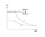
ここで、図4は直流電源Eの電源投入から移行期間を経て安定点灯に至る時間と入力電力(同図における曲線イ)及び出力電力(同図における曲線ロ)との関係を示している。従来では出力電力が増大する移行期間に入力電力も増大し、特に直流電源Eからの入力電圧が低下した場合においては回路損失が非常に大きくなってしまっていたが、本実施形態では、移行期間における回路損失が入力電圧に応じた制限値を越えないように出力電力を制御しているため、入力電力が増大し過ぎるのを防ぐことができる。その結果、入力電流の増大も抑制されるため、回路部品として従来よりも電流容量の小さいものが利用可能となる。
【0029】
(実施形態3)
図5に本発明の実施形態3のブロック図を示す。但し、本実施形態の基本回路構成は実施形態1と共通であるので、共通する構成要素には同一の符号を付して説明を省略する。
【0030】
本実施形態は、DC/DCコンバータ1の入力電圧を分圧抵抗R4,R5で分圧した電圧からDC/DCコンバータ1の入力電圧を検出する入力電圧検出回路57を制御回路5に設け、入力電圧検出回路57で検出される入力電圧が所定値を下回ると回路損失算出回路56から発振回路53に対して出力信号を出力して制御回路5による出力抑制制御動作が行われ、入力電圧が所定値を上回ると回路損失算出回路56から発振回路53への出力信号を停止して制御回路5による定常制御動作が行われるようにした点に特徴がある。
【0031】
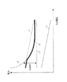
図6は直流電源Eからの入力電圧と回路損失との関係を示しており、曲線イが出力抑制制御動作を行わない場合の特性を表し、曲線ロが出力抑制制御動作を行った場合の特性を表している。通常、入力電圧が6V〜20Vの範囲で放電灯4が安定点灯し、バッテリからなる直流電源Eの定格電圧近傍(12V〜14V)で最も高い回路効率となるように回路が設計されているため、入力電圧が上記定格電圧よりも低下すると回路損失が増加することになる。ここで、回路損失の制限値をL0としたときにこの制限値L0となる入力電圧の所定値をV0(例えば、9V)とすれば、制御回路5では入力電圧検出回路57で検出する入力電圧が所定値V0を下回った場合に出力抑制制御動作を行って回路損失が制限値L0を越えないようにDC/DCコンバータ1の出力電力を抑制する。また、入力電圧検出回路57で検出する入力電圧が所定値V0を上回った場合には制御回路5が出力抑制制御動作から定常制御動作に切り換えて放電灯4への供給電力を略一定に制御する。
【0032】
而して、図6に示すように出力抑制制御動作を行わない場合には入力電圧の低下とともに回路損失が増大して回路部品の温度が上昇してしまうことになるが、本実施形態では入力電圧が所定値を下回ると制御回路5にて出力抑制制御動作を行って回路損失が制限値L0を越えないようにして回路部品の温度上昇を抑えることができる。
【0033】
ところで、制御回路5において入力電圧検出回路57が検出する入力電圧に応じて制限値を可変するようにしても良い。すなわち、入力電圧が所定の閾値V1を下回る場合の回路損失の制限値をL2、入力電圧が閾値V1を上回る場合の回路損失の制限値をL1(<L2)とし、閾値V1を境にして制限値をL1とL2で切り換えるようにすれば、制限値を一定とするよりも広範な入力電圧範囲で回路部品の温度上昇を抑えることができる。なお、図7における曲線イが出力抑制制御動作を行わない場合の回路損失の特性を表し、曲線ロが出力抑制制御動作を行った場合の回路損失の特性を表している。
【0034】
(実施形態4)
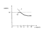
本実施形態は実施形態2と同一の回路構成を有し、制御回路7にて回路損失が所定の制限値を越えないようにDC/DCコンバータ1を制御するとともに、入力電圧検出回路8で検出する入力電圧が所定値を越える場合には制限値を一定とし、入力電圧検出回路8で検出する入力電圧が所定値を下回る場合には入力電圧に応じて制限値を可変する点に特徴がある。すなわち、図8に示すように入力電圧が所定の閾値V2(直流電源Eの定格電圧12Vよりも低い値)よりも高い場合の回路損失の制限値を一定値L3とし、入力電圧が閾値V2よりも低い場合にV2〜6Vの範囲で入力電圧に応じて回路損失の制限値をL3〜L4(>L3)の範囲で可変すれば、入力電圧の変化に対して回路損失の低減を連続的に行うことができ、回路部品の温度上昇をきめ細かく抑えることができる。ここで、図8における曲線イが回路損失の制限を行わない場合の回路損失の特性を表し、曲線ロが本実施形態の回路損失制限制御を行った場合の回路損失の特性を表している。
【0035】
而して、定常点灯時には出力電力が略一定となるように制御回路7がDC/DCコンバータ1を制御しているが、低入力電圧時にはDC/DCコンバータ1やインバータ回路2の性能上電流が増えて回路損失が急激に増大することになる。そこで本実施形態では、入力電圧に反比例した許容回路損失曲線を作成し、この許容回路損失曲線と入力電圧に基づいて回路損失の制限値を設定することにより、放電灯4が消灯しない程度に出力電力を低減する制御を制御回路7にて行っている。
【0036】
次に、図9のフローチャートを参照して放電灯4の定常点灯時における制御回路7の動作をさらに詳しく説明する。
【0037】
まず、直流電源Eから電源供給が開始されると制御回路7のマイクロコンピュータが初期設定を行った後、入力電圧検出回路8、入力電流検出回路9、出力電圧検出回路10、出力電流検出回路11からそれぞれ入力電圧検出信号、入力電流検出信号、出力電圧検出信号、出力電流検出信号を読み込む(図9のF1)。そして、入力電力演算部75が入力電圧検出信号で示される入力電圧と入力電流検出信号で示される入力電流を乗算してDC/DCコンバータ1の入力電力を演算し(図9のF2)、同じく出力電力演算部71が出力電圧検出信号で示される出力電圧と出力電流検出信号で示される出力電流を乗算してDC/DCコンバータ1の出力電力を演算する(図9のF3)。回路損失算出部76では上記入力電力と出力電力を減算することで回路損失を算出し、算出した回路損失を比較部78に与える(図9のF4)。一方、電力指令値設定部72ではマイクロコンピュータの内蔵メモリに格納されている出力電力指令値テーブルから出力電力指令値を読み出して設定し、ランプ電流指令値演算部73に与える(図9のF5)。但し、ここでは放電灯4が定常点灯している状態であるから出力電力指令値は定常点灯時に対応した一定値となる。
【0038】
ここで、入力電圧と許容回路損失曲線との関係を表したデータテーブルが予め内蔵のメモリ等に格納されており、回路損失制限値決定部77では入力電圧検出信号と上記データテーブルから回路損失の制限値を設定する(図9のF6)。さらに、ランプ電流指令値演算部73が出力電力指令値を出力電圧検出信号で示されるランプ電圧で除算することによりランプ電流指令値を演算し(図9のF7)、誤差増幅部74にて出力電流検出信号で示されるランプ電流をランプ電流指令値から減算した電流誤差値を求めて点灯制御回路79に与える(図9のF8)。そして、比較部78にて回路損失制限値決定部77で決定した回路損失の制限値と回路損失算出部76で算出した回路損失とを比較し(図9のF9)、回路損失が制限値を越える場合に点灯制御回路79に対して点灯制御停止命令を与え、点灯制御回路79による点灯制御が行われずに入力電圧検出信号等を読み込む処理(図9のF1)に戻る。また、回路損失が制限値を越えない場合には点灯制御停止命令を与えず、点灯制御回路79が電流誤差値に基づいて駆動回路70に対して点灯制御信号を出力する(図9のF10)。
【0039】
ここで、図10は直流電源Eの入力電圧と入力電力及び出力電力との関係を示している。なお、同図における曲線イは回路損失制限を行わない場合の入力電力、曲線ロは出力電力、曲線ハは許容回路損失曲線、点線ニは出力電力と許容回路損失曲線で表される回路損失の制限値とから導かれる入力電力の上限値、さらに曲線ホは回路損失制限を行った場合の入力電力の特性をそれぞれを示している。従来では低入力電圧時に回路損失が増大し、出力電力を略一定に保つために入力電流が増えすぎてしまっていた。しかしながら本実施形態では、入力電圧に応じて回路損失の制限値を可変し、回路損失が入力電圧に応じた制限値を越えないように出力電力を制御しているため、入力電力が増大し過ぎるのを防ぐことができ、その結果、入力電流の増大も抑制されて回路損失を低減することができる。
【0040】
【発明の効果】
請求項1の発明は、直流電源と、直流電源の直流電力を電力変換して放電灯に供給する電力変換手段と、この電力変換手段を制御して放電灯に略一定電力を供給する制御手段とを備えた放電灯点灯装置において、直流電源からの入力電力を検出する入力電力検出手段と、放電灯に供給する出力電力を検出する出力電力検出手段とを設け、制御手段は入力電力と出力電力から求まる回路損失が所定値を上回ると当該回路損失に応じて前記略一定電力を低減するので、電力変換手段から放電灯に供給する略一定電力を低減することで回路損失を低減し、小型化やランプ近傍への設置を可能としながら回路部品の温度上昇を抑えて特性劣化や破壊等の不具合の発生を防ぐことができるという効果がある。
【0041】
請求項2の発明は、請求項1の発明において、制御手段は、放電灯の始動後から放電灯が安定点灯して放電灯への供給電力を前記略一定電力に調整するまでの移行期間に、回路損失に応じて出力電力を抑制するので、入力電流が最も大きくなる移行期間における入力電流ピークを低下させることができ、その結果、電力変換手段を構成する回路部品に電流容量の小さい部品を使用することができるという効果がある。
【0042】
請求項3の発明は、請求項1の発明において、電力変換手段への入力電圧を検出する入力電圧検出手段を備え、制御手段は入力電圧検出手段が検出する入力電圧が所定値を下回ると回路損失に応じて前記略一定電力を低減するので、最も回路損失が増大する入力電圧低下時に回路部品の温度上昇を抑えることができるという効果がある。
【0043】
請求項4の発明は、請求項1の発明において、制御手段は、回路損失が所定の制限値を越えないように前記略一定電力を低減するので、回路部品の温度上昇を簡単な制御で抑えることができるという効果がある。
【0044】
請求項5の発明は、請求項1の発明において、電力変換手段への入力電圧を検出する入力電圧検出手段を備え、制御手段は、回路損失が所定の制限値を越えないように電力変換手段を制御するとともに入力電圧検出手段が検出する入力電圧に応じて制限値を可変するので、制限値を一定とするよりも広範な入力電圧範囲で回路部品の温度上昇を抑えることができるという効果がある。
【0045】
請求項6の発明は、請求項1の発明において、電力変換手段への入力電圧を検出する入力電圧検出手段を備え、制御手段は、回路損失が所定の制限値を越えないように電力変換手段を制御するとともに、入力電圧検出手段が検出する入力電圧が所定値を越える場合には制限値を一定とし、入力電圧検出手段が検出する入力電圧が所定値を下回る場合には当該入力電圧に応じて制限値を可変するので、入力電圧の変化に対して回路損失の低減を連続的に行うことができ、回路部品の温度上昇をきめ細かく抑えることができるという効果がある。
【図面の簡単な説明】
【図1】実施形態1を示すブロック図である。
【図2】実施形態2を示すブロック図である。
【図3】同上の動作説明用のフローチャートである。
【図4】同上の動作説明図である。
【図5】実施形態3を示すブロック図である。
【図6】同上の動作説明図である。
【図7】同上の動作説明図である。
【図8】実施形態4の動作説明図である。
【図9】同上の動作説明用のフローチャートである。
【図10】同上の動作説明図である。
【図11】従来例を示すブロック図である。
【符号の説明】
1 DC/DCコンバータ
2 インバータ回路
3 イグナイタ回路
4 放電灯
5 制御回路
51 電力演算部
52 誤差増幅部
53 発振回路
54 駆動回路
55 入力電力演算部
56 回路損失算出回路[0001]
BACKGROUND OF THE INVENTION
The present invention relates to a discharge lamp lighting device having a discharge lamp such as a metal halide lamp as a load.
[0002]
[Prior art]
In recent years, metal halide lamps are often used as discharge lamps for automobile headlamps. When a metal halide lamp (hereinafter abbreviated as “lamp”) is used for a headlamp, due to the nature of its use, it is necessary to shorten the time until the luminous flux stabilizes after the lamp is started. Must be supplied. Then, after the luminous flux is stabilized, constant power control is performed so that the rated power value of the lamp is not exceeded with respect to the power supply voltage fluctuation of the power supply (vehicle battery).
[0003]
FIG. 11 is a block diagram showing an example of a conventional discharge lamp lighting device. This conventional apparatus includes, for example, a DC power source E composed of a battery such as a 12V system or a 24V system, a DC /
[0004]
The
[0005]
By the way, due to the downsizing of the discharge lamp lighting device, the heat dissipating area of the heat generated by the circuit components is also reduced. It is getting bigger. Moreover, since the degree of freedom of the installation location is increased due to the miniaturization of the discharge lamp lighting device, the discharge lamp lighting device is frequently installed in the vicinity of the lamp. As a result, the temperature of the circuit component further increases due to the heat generated by the lamp, and therefore it is required to suppress the temperature increase of the circuit component in order to prevent the characteristic deterioration and destruction of the circuit component due to the heat.
[0006]
Therefore, in order to prevent an increase in circuit loss due to battery voltage fluctuation, use circuit components with low loss to reduce the circuit loss of the entire device, or use circuit components with large allowable loss (maximum allowable loss). Measures are taken such as increasing the tolerance for circuit loss by adopting a structure with high heat dissipation.
[0007]
[Problems to be solved by the invention]
However, in the conventional measures as described above, circuit components having good characteristics (low loss) and circuit components having a large allowable loss must be used, leading to an increase in cost of the discharge lamp lighting device. is there. Further, a structure that achieves miniaturization and improved heat dissipation at the same time is also costly. In addition, when installed in the vicinity of the lamp, there is a possibility that the characteristic deterioration and destruction of the circuit components cannot be prevented even if the above-described measures are taken.
[0008]
The present invention has been made in view of the above problems, and the object of the present invention is to reduce the temperature of the circuit components while enabling downsizing and installation in the vicinity of the lamp, and to solve problems such as characteristic deterioration and destruction. An object of the present invention is to provide a discharge lamp lighting device capable of preventing the occurrence.
[0009]
[Means for Solving the Problems]
In order to achieve the above object, a first aspect of the present invention is directed to a DC power supply, power conversion means for converting the DC power of the DC power supply to supply the discharge lamp, and controlling the power conversion means to the discharge lamp. Supply almost constant power In a discharge lamp lighting device comprising a control means, an input power detection means for detecting an input power from a DC power supply and an output power detection means for detecting an output power supplied to the discharge lamp are provided, and the control means has an input power And circuit loss calculated from output power If the value exceeds the specified value, the circuit loss In response to the Reduce the substantially constant power It is characterized by Reduces substantially constant power supplied from the power conversion means to the discharge lamp As a result, the circuit loss can be reduced and the temperature rise of the circuit components can be suppressed while downsizing and installation in the vicinity of the lamp can be suppressed, thereby preventing the occurrence of defects such as characteristic deterioration and destruction.
[0010]
According to a second aspect of the present invention, in the first aspect of the present invention, the control means controls the power supplied to the discharge lamp after the discharge lamp is stably lit after the discharge lamp is started. The substantially constant power Suppress output power according to circuit loss during the transition period until adjustment Ruko The input current peak in the transition period in which the input current becomes the largest can be reduced, and as a result, a component having a small current capacity can be used as the circuit component constituting the power conversion means.
[0011]
According to a third aspect of the present invention, in the first aspect of the present invention, the control device includes an input voltage detection unit that detects an input voltage to the power conversion unit, and the control unit is configured to provide a circuit when the input voltage detected by the input voltage detection unit falls below a predetermined value. Depending on the loss Reduce the substantially constant power The temperature rise of the circuit components can be suppressed when the input voltage is lowered when the circuit loss increases most.
[0012]
According to a fourth aspect of the present invention, in the first aspect of the present invention, the control means prevents the circuit loss from exceeding a predetermined limit value. Reduce the substantially constant power The temperature rise of the circuit components can be suppressed by simple control.
[0013]
According to a fifth aspect of the present invention, there is provided the input voltage detecting means for detecting an input voltage to the power converting means in the first aspect of the invention, and the control means is a power converting means for preventing the circuit loss from exceeding a predetermined limit value. The limit value is variable according to the input voltage detected by the input voltage detection means, and the temperature rise of the circuit components can be suppressed over a wider input voltage range than the limit value is constant. .
[0014]
According to a sixth aspect of the present invention, in the first aspect of the present invention, the control device further includes an input voltage detection unit that detects an input voltage to the power conversion unit, and the control unit includes the power conversion unit so that the circuit loss does not exceed a predetermined limit value. The limit value is fixed when the input voltage detected by the input voltage detection means exceeds a predetermined value, and the input voltage detected by the input voltage detection means is determined according to the input voltage when the input voltage is lower than the predetermined value. The limit value can be varied, and the circuit loss can be continuously reduced with respect to the change of the input voltage, and the temperature rise of the circuit components can be finely suppressed.
[0015]
DETAILED DESCRIPTION OF THE INVENTION
(Embodiment 1)
FIG. 1 shows a block diagram of
[0016]
In the present embodiment, a DC power source E composed of an in-vehicle battery, a DC /
[0017]
Further, the
[0018]
Thus, like the
[0019]
The above description is a control operation when the circuit loss calculated by the circuit
[0020]
As described above, in the present embodiment, the input power from the DC power source E is detected, the output power supplied to the discharge lamp 4 is detected, and the output power is determined according to the circuit loss obtained from these input power and output power. Since the
[0021]
(Embodiment 2)
FIG. 2 shows a block diagram of
[0022]
As shown in FIG. 2, the input voltage of the DC /
[0023]
In addition, the control circuit 7 in the present embodiment has a microcomputer as a main component, and realizes the functions of the following units by executing a program stored in a built-in memory or the like. The output
[0024]
On the other hand, the power command
[0025]
Next, the operation of the control circuit 7 in this embodiment will be described in more detail with reference to the flowchart of FIG.
[0026]
First, when power supply from the DC power source E is started, the microcomputer of the control circuit 7 performs initial setting, and then the input
[0027]
On the other hand, the power command
[0028]
Here, FIG. 4 shows the relationship between the time from the power-on of the DC power supply E to the stable lighting through the transition period, the input power (curve A in the figure), and the output power (curve B in the figure). Conventionally, the input power also increases during the transition period in which the output power increases. In particular, when the input voltage from the DC power supply E decreases, the circuit loss has become very large. Since the output power is controlled so that the circuit loss does not exceed the limit value according to the input voltage, it is possible to prevent the input power from increasing excessively. As a result, since an increase in input current is also suppressed, a circuit component having a smaller current capacity than the conventional one can be used.
[0029]
(Embodiment 3)
FIG. 5 shows a block diagram of
[0030]
In this embodiment, the
[0031]
FIG. 6 shows the relationship between the input voltage from the DC power source E and the circuit loss. The curve A represents the characteristic when the output suppression control operation is not performed, and the curve B represents the characteristic when the output suppression control operation is performed. Represents. Normally, the discharge lamp 4 is stably lit when the input voltage is in the range of 6V to 20V, and the circuit is designed to have the highest circuit efficiency in the vicinity of the rated voltage (12V to 14V) of the DC power supply E composed of a battery. When the input voltage is lower than the rated voltage, the circuit loss increases. Here, if the predetermined value of the input voltage that becomes the limit value L0 when the limit value of the circuit loss is L0 is V0 (for example, 9V), the
[0032]
Thus, as shown in FIG. 6, when the output suppression control operation is not performed, the circuit loss increases as the input voltage decreases and the temperature of the circuit component rises. When the voltage falls below a predetermined value, the output suppression control operation is performed by the
[0033]
Incidentally, the limit value may be varied in the
[0034]
(Embodiment 4)
The present embodiment has the same circuit configuration as that of the second embodiment. The control circuit 7 controls the DC /
[0035]
Thus, the control circuit 7 controls the DC /
[0036]
Next, the operation of the control circuit 7 during steady lighting of the discharge lamp 4 will be described in more detail with reference to the flowchart of FIG.
[0037]
First, when power supply from the DC power source E is started, the microcomputer of the control circuit 7 performs initial setting, and then the input
[0038]
Here, a data table representing the relationship between the input voltage and the allowable circuit loss curve is stored in advance in a built-in memory or the like, and the circuit loss limit
[0039]
Here, FIG. 10 shows the relationship between the input voltage of the DC power source E, the input power, and the output power. Curve A in the figure is the input power when the circuit loss is not limited, curve B is the output power, curve C is the allowable circuit loss curve, dotted line D is the circuit loss expressed by the output power and the allowable circuit loss curve. The upper limit value of the input power derived from the limit value, and the curve E indicates the characteristics of the input power when the circuit loss is limited. Conventionally, the circuit loss increases at a low input voltage, and the input current increases too much to keep the output power substantially constant. However, in this embodiment, the limit value of the circuit loss is varied according to the input voltage, and the output power is controlled so that the circuit loss does not exceed the limit value according to the input voltage. As a result, an increase in input current is also suppressed and circuit loss can be reduced.
[0040]
【The invention's effect】
The invention of
[0041]
According to a second aspect of the present invention, in the first aspect of the present invention, the control means controls the power supplied to the discharge lamp after the discharge lamp is stably lit after the discharge lamp is started. The substantially constant power Suppress output power according to circuit loss during the transition period until adjustment Ru Therefore, the input current peak in the transition period in which the input current becomes maximum can be reduced, and as a result, there is an effect that a component having a small current capacity can be used as the circuit component constituting the power conversion means.
[0042]
According to a third aspect of the present invention, in the first aspect of the present invention, the control device includes an input voltage detection unit that detects an input voltage to the power conversion unit, and the control unit is configured to provide a circuit when the input voltage detected by the input voltage detection unit falls below a predetermined value. Depending on the loss Reduce the substantially constant power Therefore, there is an effect that it is possible to suppress the temperature rise of the circuit components when the input voltage is lowered when the circuit loss is most increased.
[0043]
According to a fourth aspect of the present invention, in the first aspect of the present invention, the control means prevents the circuit loss from exceeding a predetermined limit value. Reduce the substantially constant power Therefore, there is an effect that the temperature rise of the circuit component can be suppressed by simple control.
[0044]
According to a fifth aspect of the present invention, there is provided the input voltage detecting means for detecting an input voltage to the power converting means in the first aspect of the invention, and the control means is a power converting means for preventing the circuit loss from exceeding a predetermined limit value. Since the limit value is varied according to the input voltage detected by the input voltage detecting means, the temperature rise of the circuit components can be suppressed over a wider input voltage range than when the limit value is constant. is there.
[0045]
According to a sixth aspect of the present invention, in the first aspect of the present invention, the control device further includes an input voltage detection unit that detects an input voltage to the power conversion unit, and the control unit includes the power conversion unit so that the circuit loss does not exceed a predetermined limit value. And the limit value is fixed when the input voltage detected by the input voltage detection means exceeds a predetermined value, and the input voltage detected by the input voltage detection means is determined according to the input voltage when the input voltage is lower than the predetermined value. Since the limit value is variable, the circuit loss can be continuously reduced with respect to the change of the input voltage, and the temperature rise of the circuit components can be finely suppressed.
[Brief description of the drawings]
FIG. 1 is a block diagram illustrating a first embodiment.
FIG. 2 is a block diagram showing a second embodiment.
FIG. 3 is a flowchart for explaining the operation of the above.
FIG. 4 is an operation explanatory view of the above.
FIG. 5 is a block diagram showing a third embodiment.
FIG. 6 is an operation explanatory view of the above.
FIG. 7 is an operation explanatory diagram of the above.
FIG. 8 is an operation explanatory diagram of the fourth embodiment.
FIG. 9 is a flowchart for explaining the operation.
FIG. 10 is an operation explanatory view of the above.
FIG. 11 is a block diagram showing a conventional example.
[Explanation of symbols]
1 DC / DC converter
2 Inverter circuit
3 Igniter circuit
4 Discharge lamp
5 Control circuit
51 Power calculator
52 Error amplifier
53 Oscillator circuit
54 Drive circuit
55 Input power calculator
56 Circuit loss calculation circuit
Claims (6)
直流電源からの入力電力を検出する入力電力検出手段と、放電灯に供給する出力電力を検出する出力電力検出手段とを設け、制御手段は入力電力と出力電力から求まる回路損失が所定値を上回ると当該回路損失に応じて前記略一定電力を低減することを特徴とする放電灯点灯装置。A discharge lamp lighting comprising a DC power supply, power conversion means for converting DC power of the DC power supply to supply to the discharge lamp, and control means for controlling the power conversion means to supply substantially constant power to the discharge lamp In the device
Input power detection means for detecting input power from the DC power supply and output power detection means for detecting output power supplied to the discharge lamp are provided, and the control means has a circuit loss obtained from the input power and output power exceeding a predetermined value. And the substantially constant power is reduced according to the circuit loss .
Priority Applications (1)
| Application Number | Priority Date | Filing Date | Title |
|---|---|---|---|
| JP2001005710A JP4524924B2 (en) | 2001-01-12 | 2001-01-12 | Discharge lamp lighting device |
Applications Claiming Priority (1)
| Application Number | Priority Date | Filing Date | Title |
|---|---|---|---|
| JP2001005710A JP4524924B2 (en) | 2001-01-12 | 2001-01-12 | Discharge lamp lighting device |
Publications (2)
| Publication Number | Publication Date |
|---|---|
| JP2002216987A JP2002216987A (en) | 2002-08-02 |
| JP4524924B2 true JP4524924B2 (en) | 2010-08-18 |
Family
ID=18873719
Family Applications (1)
| Application Number | Title | Priority Date | Filing Date |
|---|---|---|---|
| JP2001005710A Expired - Fee Related JP4524924B2 (en) | 2001-01-12 | 2001-01-12 | Discharge lamp lighting device |
Country Status (1)
| Country | Link |
|---|---|
| JP (1) | JP4524924B2 (en) |
Families Citing this family (3)
| Publication number | Priority date | Publication date | Assignee | Title |
|---|---|---|---|---|
| JP4247868B2 (en) | 2001-09-25 | 2009-04-02 | Tdk株式会社 | Discharge lamp lighting device and discharge lamp device |
| US7880445B2 (en) | 2006-02-16 | 2011-02-01 | Summit Microelectronics, Inc. | System and method of charging a battery using a switching regulator |
| CN115515279A (en) * | 2022-10-19 | 2022-12-23 | 深圳市飞业泰电子有限公司 | LED power supply adaptive to constant input power |
Family Cites Families (6)
| Publication number | Priority date | Publication date | Assignee | Title |
|---|---|---|---|---|
| JPH06197526A (en) * | 1992-12-25 | 1994-07-15 | Canon Inc | Electronics |
| JP3536421B2 (en) * | 1995-04-25 | 2004-06-07 | 松下電工株式会社 | Power supply |
| JPH1198857A (en) * | 1997-09-16 | 1999-04-09 | Yaskawa Electric Corp | Power converter using multiple pulse width modulation |
| JPH11262256A (en) * | 1998-03-13 | 1999-09-24 | Matsushita Electric Works Ltd | Power unit and electric discharge lamp turning-on device |
| JPH11326428A (en) * | 1998-05-19 | 1999-11-26 | Sony Tektronix Corp | Parameter measuring device for inverter circuit |
| JP2001078443A (en) * | 1999-09-07 | 2001-03-23 | Ohira Denshi Kk | Switching power supply including defective power protection circuit |
-
2001
- 2001-01-12 JP JP2001005710A patent/JP4524924B2/en not_active Expired - Fee Related
Also Published As
| Publication number | Publication date |
|---|---|
| JP2002216987A (en) | 2002-08-02 |
Similar Documents
| Publication | Publication Date | Title |
|---|---|---|
| US8963425B2 (en) | Power supply device, lamp fitting, and vehicle | |
| JP4325620B2 (en) | Discharge lamp lighting device, lighting device, projector | |
| JP5411668B2 (en) | Lighting device, high-intensity discharge lamp lighting device, semiconductor light source lighting device, headlamp equipped with the same, and vehicle | |
| JP4524924B2 (en) | Discharge lamp lighting device | |
| US6815912B2 (en) | Discharge lamp lighting apparatus and discharge lamp apparatus | |
| JP4480073B2 (en) | Discharge lamp lighting device | |
| CN103582272B (en) | Discharging lamp electronic rectifier, the ligthing paraphernalia with this ballast and vehicle | |
| JP2013222549A (en) | Discharge lamp lighting device, and on-vehicle lighting system and vehicle having the same | |
| JP2005158459A (en) | Electrodeless discharge lamp lighting device and electrodeless discharge lamp device | |
| WO2007072925A1 (en) | Discharge lamp lighting device and image display device | |
| JP3900831B2 (en) | Discharge lamp lighting device | |
| US8080949B2 (en) | HID ballast with integrated voltage multiplier and lamp temperature compensation | |
| JP2013016855A (en) | Electric power unit and lighting fixture, vehicle | |
| JP3807191B2 (en) | Discharge lamp lighting device | |
| JP3326955B2 (en) | Discharge lamp lighting device | |
| JP4083895B2 (en) | Discharge lamp lighting device | |
| JP2014157782A (en) | Lighting device and lighting fixture using the same | |
| JP4040769B2 (en) | Discharge lamp lighting device | |
| JP2004127721A (en) | Illuminating apparatus | |
| US7626341B2 (en) | Discharge lamp lighting apparatus | |
| JP4794921B2 (en) | Discharge lamp lighting device | |
| JP2006252921A (en) | Discharge lamp lighting circuit | |
| JP3888062B2 (en) | Discharge lamp lighting device | |
| US20130271003A1 (en) | Discharge lamp lighting device, and headlight and vehicle including same | |
| JP2000030883A (en) | Discharge lamp lighting device |
Legal Events
| Date | Code | Title | Description |
|---|---|---|---|
| A621 | Written request for application examination |
Free format text: JAPANESE INTERMEDIATE CODE: A621 Effective date: 20071115 |
|
| A977 | Report on retrieval |
Free format text: JAPANESE INTERMEDIATE CODE: A971007 Effective date: 20090520 |
|
| A131 | Notification of reasons for refusal |
Free format text: JAPANESE INTERMEDIATE CODE: A131 Effective date: 20090526 |
|
| A02 | Decision of refusal |
Free format text: JAPANESE INTERMEDIATE CODE: A02 Effective date: 20091215 |
|
| A521 | Request for written amendment filed |
Free format text: JAPANESE INTERMEDIATE CODE: A523 Effective date: 20100315 |
|
| A911 | Transfer to examiner for re-examination before appeal (zenchi) |
Free format text: JAPANESE INTERMEDIATE CODE: A911 Effective date: 20100325 |
|
| TRDD | Decision of grant or rejection written | ||
| A01 | Written decision to grant a patent or to grant a registration (utility model) |
Free format text: JAPANESE INTERMEDIATE CODE: A01 Effective date: 20100511 |
|
| A01 | Written decision to grant a patent or to grant a registration (utility model) |
Free format text: JAPANESE INTERMEDIATE CODE: A01 |
|
| A61 | First payment of annual fees (during grant procedure) |
Free format text: JAPANESE INTERMEDIATE CODE: A61 Effective date: 20100524 |
|
| FPAY | Renewal fee payment (event date is renewal date of database) |
Free format text: PAYMENT UNTIL: 20130611 Year of fee payment: 3 |
|
| R151 | Written notification of patent or utility model registration |
Ref document number: 4524924 Country of ref document: JP Free format text: JAPANESE INTERMEDIATE CODE: R151 |
|
| FPAY | Renewal fee payment (event date is renewal date of database) |
Free format text: PAYMENT UNTIL: 20130611 Year of fee payment: 3 |
|
| LAPS | Cancellation because of no payment of annual fees |