JP4040769B2 - Discharge lamp lighting device - Google Patents
Discharge lamp lighting device Download PDFInfo
- Publication number
- JP4040769B2 JP4040769B2 JP32163698A JP32163698A JP4040769B2 JP 4040769 B2 JP4040769 B2 JP 4040769B2 JP 32163698 A JP32163698 A JP 32163698A JP 32163698 A JP32163698 A JP 32163698A JP 4040769 B2 JP4040769 B2 JP 4040769B2
- Authority
- JP
- Japan
- Prior art keywords
- reference voltage
- discharge lamp
- circuit
- lighting device
- current
- Prior art date
- Legal status (The legal status is an assumption and is not a legal conclusion. Google has not performed a legal analysis and makes no representation as to the accuracy of the status listed.)
- Expired - Fee Related
Links
Images
Landscapes
- Circuit Arrangements For Discharge Lamps (AREA)
- Inverter Devices (AREA)
Description
【0001】
【発明の属する技術分野】
この発明は、インバータ回路からの高周波電力によって放電灯を点灯させる放電灯点灯装置に関するものである。
【0002】
【従来の技術】
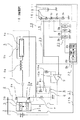
図10に、従来の放電灯点灯装置の回路図を示す。図において、1は商用電源を整流、平滑化して直流電流を得る直流電源、2はMOS FET等のスイッチング素子2a、2bから成るインバ−タ回路、3はインバータ回路2を駆動するインバータ駆動回路、4はインバータ回路2の出力側に接続された結合コンデンサ、5はチョ−クコイル5a、始動コンデンサ5bおよび放電灯5cから成る放電灯負荷回路、6は検出抵抗7と、抵抗8aおよびコンデンサ8bを備えた積分回路8(ハイパスフィルタ−)から構成され放電灯負荷回路5に供給される正味電流を検出する電流検出回路、9は誤差増幅器、10aおよび10bは誤差増幅器9での積分用の抵抗およびコンデンサであり、誤差増幅器9の反転入力端には積分回路8の出力電圧が、また、非反転入力端には安定化された基準電圧用直流電源11および分割抵抗12、13とを備えた基準電圧回路14から基準電圧が入力され、上記の2つの電圧の差が誤差増幅器9で増幅されて制御信号としてインバ−タ駆動回路3にフィードバックされている。
【0003】
なお、商用電源から直流電流を得る場合の直流電源1の構成例を図11に示す。図に示すように、商用電源1aから出力された交流電流はダイオ−ドブリッジ1bで全波整流された後、平滑コンデンサ1cで平滑化され、直流電流として負荷回路に出力されるよう構成されている。
【0004】
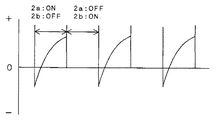
以下、この図10に示した従来例の回路の動作について説明する。図において、インバータ駆動回路3によりインバ−タ回路2が駆動されると直流電源1から供給される直流電流が高周波電流に変換され、放電灯負荷回路5に供給されて、放電灯5cが点灯する。この時、放電灯負荷回路5には結合コンデンサ4が接続されているため、スイッチング素子2aおよび2bのON、OFFに連動して、検出抵抗7には、図12に示すような順方向および逆方向(回生方向)に交流電流が流れることになり、回路損失を無視すると、この有効成分(順および逆方向の電流の和。以下、正味電流と呼ぶ)が放電灯5cで電力として消費される。
【0005】
一方、検出抵抗7によって検出された電流は、積分回路8で順方向および逆方向の電流の和(正味電流)が検出されて、対応する電圧が誤差増幅器9の反転入力端に入力される。また、誤差増幅器9の非反転入力端には、基準電圧回路14から基準電圧用直流電源11の電圧を分割抵抗12及び13で分割して生成した基準電圧が入力されており、誤差増幅器9では、この基準電圧と積分回路8からの出力電圧との電圧差が増幅されるとともに、積分用の抵抗10aおよびコンデンサ10bによって積分され、インバ−タ駆動回路3に制御信号としてフィードバックされて、インバ−タ駆動回路3でインバータ回路2のスイッチング周波数が制御されることにより、直流電源1から放電灯負荷回路5に供給される高周波電流が調整される。こうして、放電灯負荷回路5に供給される高周波電流がインバ−タ回路2のスイッチング周波数で制御されるため、インバ−タ回路2のスイッチング周波数を制御して積分回路8の出力電圧が基準電圧に等しくなるよう保持すれば、直流電源1の出力電圧が一定の場合、放電灯5cに供給される電力を一定に保つことができる。
【0006】
【発明が解決しようとする課題】
しかしながら、上記図10に示した従来の放電灯点灯装置では、基準電圧回路14から出力される基準電圧が点灯装置毎に固定されていたため、異なる定格値を有する放電灯に対応するためには、チョークコイル5aや始動コンデンサ5b等の部品をあらかじめ複数種類用意しておき、装着する放電灯5cの定格値に合わせて回路定数を変更したり、商品群をラインアップする場合に放電灯5cの定格値に対応した多種類の放電灯点灯装置を用意しておく必要があり、生産時の部品管理や製品の在庫管理が煩雑になり、管理コストが高くなるといった問題点があった。
【0007】
また、放電灯点灯装置を設置した後に、照度アップや省電力等の目的で異なる定格値の放電灯に変更する場合には、放電灯点灯装置を新たに交換、設置する必要があり、購入費用や放電灯点灯装置の交換に要する運用コストが高くなるといった問題点も有していた。
【0008】
この発明は、従来装置の上記のような問題点を解消するためになされたもので、この発明の第1の目的は、1つの放電灯点灯装置で複数の異なる定格値を有する放電灯に自動的に適合できるとともに、設置後においても放電灯の定格値の変更に自動的に対応され、生産時の部品管理等の管理コストや設置後の運用コスト等の削減が可能な放電灯点灯装置を提供することを目的とする。
【0009】
また、この発明の第2の目的は、放電灯の定格値の変更を自動的に行うことにより、定格値の変更が容易であるとともに、電気的な知識がない場合にも確実に定格値が変更でき、また、点灯時にも放電灯に定格値を超える電流が流れることを防止して、放電灯が短寿命となる心配のない放電灯点灯装置を提供することを目的とする。
【0010】
また、この発明の第3の目的は、同一の放電灯で複数の定格値を有する放電灯にも適合できる放電灯点灯装置を提供することを目的とする。
【0011】
さらに、この発明の第4の目的は、定格値の変更に伴う放電灯の明るさ(光出力)の急激な変化を抑制し、使用時の快適性にも優れた放電灯点灯装置を提供することを目的とする。
【0012】
【課題を解決するための手段】
この発明に係る放電灯点灯装置は、上記の目的を達成するために、直流電源と、上記直流電源から供給される直流を高周波電流に変換するインバータ回路と、上記インバータ回路からの高周波電流により放電灯を点灯させる放電灯負荷回路と、上記インバータ回路から上記放電灯負荷回路に供給される電流を検出する電流検出回路と、基準電圧を発生する基準電圧回路と、上記電流検出回路からの出力と上記基準電圧回路からの基準電圧に基づいて制御信号を生成する誤差増幅器と、上記誤差増幅器からの制御信号に基づいて上記インバータ回路のスイッチング周波数を制御し、上記インバータ回路から上記放電灯負荷回路に供給される電流を制御するインバータ駆動回路とを備えた放電灯点灯装置において、上記インバータ回路のスイッチング周波数を検出する周波数検出手段を設けるとともに、上記基準電圧回路を放電灯の定格値に対応した複数の異なる基準電圧を出力できるよう構成し、さらに、上記基準電圧回路には、上記周波数検出手段によって検出されたスイッチング周波数に基づいて上記放電灯負荷回路に装着された放電灯の定格値を識別し、この定格値に適合した基準電圧を自動的に選択可能な基準電圧選択手段を設けたものである。
【0013】
また、この発明に係る放電灯点灯装置は、上記基準電圧選択手段が、上記周波数検出手段から出力されるスイッチング周波数と上記電流検出回路から出力される上記放電灯負荷回路に供給される正味電流値とに基づいて、上記放電灯負荷回路に装着された放電灯の定格値を識別するよう構成したものである。
【0014】
また、この発明に係る放電灯点灯装置は、上記基準電圧回路を、基準電圧用直流電源と上記基準電圧用直流電源の電圧を分割する分割抵抗とを備え、あらかじめ設定された放電灯の定格値に対応した複数の異なる基準電圧を発生する基準電圧発生部と、上記周波数検出手段からの出力に基づいて上記放電灯負荷回路に装着された放電灯の定格値を識別し、上記基準電圧発生部で生成する基準電圧の中からこの定格値に適合した基準電圧を自動的に選択する基準電圧選択手段とから構成したものである。
【0015】
また、この発明に係る放電灯点灯装置は、上記基準電圧回路を、基準電圧用直流電源と、上記基準電圧用直流電源の電圧を分割する分割抵抗と、基準電圧を選択するスイッチ部および上記スイッチ部を制御するスイッチ制御部とを備えた基準電圧選択手段とから構成するとともに、上記スイッチ部の各スイッチを上記分割抵抗に並列に接続し、上記スイッチ制御部でバイパスする分割抵抗を選択することにより、上記基準電圧回路から出力される基準電圧が選択されるよう構成したものである。
【0016】
さらに、この発明に係る放電灯点灯装置は、上記基準電圧選択手段を、上記周波数検出手段の出力をデジタルデータ化するA/D変換器と、上記インバータ回路のスイッチング周波数を記憶する記憶回路と、上記A/D変換器によって検出されたデジタルデータと上記記憶回路にあらかじめ保存されたスイッチング周波数とを比較して装着された放電灯の定格値を識別し、制御信号を出力する演算回路とを備えたスイッチ制御部と、上記演算回路からの制御信号により上記基準電圧回路から出力される基準電圧を選択するスイッチ部とから構成したものである。
【0017】
また、この発明に係る放電灯点灯装置は、放電灯点灯装置の起動時に、上記基準電圧選択手段が、上記基準電圧回路から出力可能な基準電圧のうち最も小さい正味電流に対応した基準電圧を選択するよう構成したものである。
【0018】
また、この発明に係る放電灯点灯装置は、放電灯の定格値を識別する情報を上記基準電圧選択手段に手動で入力できる外部設定手段を設けたものである。
【0019】
さらに、この発明に係る放電灯点灯装置は、上記基準電圧回路と上記誤差増幅器との間に緩衝回路を設け、上記基準電圧回路から出力される基準電圧の変更時に、上記誤差増幅器に入力される基準電圧が連続的に変化するよう構成したものである。
【0020】
また、この発明に係る放電灯点灯装置は、上記基準電圧回路を、上記誤差増幅器が実装された回路基板上に設けたものである。
【0021】
また、この発明に係る放電灯点灯装置は、上記基準電圧回路および上記誤差増幅器が実装された回路基板をケース内に収納したものである。
【0022】
【発明の実施の形態】
実施の形態1.
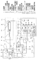
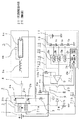
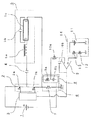
図1は、この発明の実施の形態1である放電灯点灯装置の構成を示す回路図である。図において、1は商用電源を整流、平滑化して直流電流を得る直流電源、2はMOS FET等のスイッチング素子2a、2bから成るインバ−タ回路、3は、内部に電圧によってスイッチング周波数が制御される電圧制御発振回路3a(図中、「VCO」と記載)およびドライバ3bを備え、インバータ回路2を駆動するインバータ駆動回路、4はインバータ回路2の出力側に接続された結合コンデンサ、5はチョ−クコイル5a、始動コンデンサ5bおよび放電灯5cから成る放電灯負荷回路、6は検出抵抗7と、抵抗8aおよびコンデンサ8bを備えた積分回路8(ハイパスフィルタ−)から構成され放電灯負荷回路5に供給される正味電流を検出する電流検出回路、9は誤差増幅器、10aおよび10bは誤差増幅器9での積分用の抵抗およびコンデンサであり、誤差増幅器9の反転入力端には積分回路8の出力電圧が、また、非反転入力端には基準電圧回路14から基準電圧が入力され、上記の2つの電圧の差が誤差増幅器9で増幅されて制御信号としてインバ−タ駆動回路3にフィードバックされている。
【0023】
一方、この実施の形態1では、インバータ駆動回路3には、電圧制御発振回路3aの発振周波数、すなわち、インバータ駆動回路3のスイッチング周波数を外部に出力する周波数出力端子21aが備えられ、接続線21bとともに、このスイッチング周波数に関する情報を基準電圧回路14内のスイッチ制御部22に入力する周波数検出手段21を構成している。
【0024】
また、基準電圧回路14は、安定化された基準電圧用直流電源11の電圧を分割抵抗12a、12b、12cおよび13で分割して放電灯5cの定格値(例えば、32W、40W、45W)に対応した3つの基準電圧をあらかじめ設定、生成する基準電圧発生部15と、基準電圧発生部15で生成された3つの基準電圧の中から装着された放電灯5cの定格値に適合した基準電圧を選択し誤差増幅器9に入力する基準電圧選択手段23から構成され、この基準電圧選択手段23は、3つのスイッチ20a、20b、20cから成るスイッチ部20と、接続線21bにより周波数出力端子21aから入力されたインバータ駆動回路3のスイッチング周波数に基づいて放電灯負荷回路5に装着された放電灯5cの定格値を識別し、スイッチ部20の各スイッチを自動制御するスイッチ制御部22とを備えている。
【0025】
さらに、このスイッチ制御部22の具体的構成は、図1に示すように、周波数出力端子21aからの出力をデジタル変換するA/D変換器22aと、基準電圧回路14から出力される基準電圧とインバータ駆動回路3のスイッチング周波数との関係を記憶した記憶回路22bと、上記A/D変換器22aからの出力と上記記憶回路22b内に保存された周波数データに基いて放電灯負荷回路5に装着された放電灯5cの定格値を検出し、スイッチ部20にON/OFF信号を送出する演算回路22cから構成され、この実施の形態1では、スイッチ制御部22をA/D変換機能およびメモリを内蔵したマイコンで、また、スイッチ部20を半導体スイッチにより構成している。
【0026】
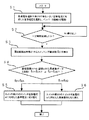
以下、この実施の形態1の動作について図1の構成図と図2のフローチャートを用いて説明する。まず、ステップS1において、この放電灯点灯装置の起動時には、スイッチ制御部22によって、スイッチ部20のスイッチのうち最も小さな正味電流を与える基準電圧に対応したスイッチ20aがONに、また、他のスイッチ20b、20cがOFFになるよう設定されている。この状態で放電灯点灯装置を起動すると、誤差増幅器9には、基準電圧回路14から最小の正味電流に対応する基準電圧が入力され、誤差増幅器9で電流検出回路6からの信号との差が増幅されてインバータ駆動回路3に入力され、インバータ駆動回路3内の電圧制御発振回路3aではこの電圧に対応してスイッチング周波数が制御され、ドライバ3bを介してインバ−タ回路2を駆動することにより、直流電源1から供給される直流電流が高周波電流に変換されて、放電灯負荷回路5に供給され、放電灯5cが点灯する。
【0027】
この時、放電灯負荷回路5には結合コンデンサ4が接続されているため、スイッチング素子2aおよび2bのON、OFFに連動して、放電灯負荷回路5には、直流電源1→スイッチング素子2a→結合コンデンサ4→放電灯負荷回路5→検出抵抗7→直流電源1なる右周りおよび結合コンデンサ4→スイッチング素子2b→放電灯負荷回路5→結合コンデンサ4なる左周りの交流電流が交互に流れることになり、この結果、検出抵抗7には図12と同様の交流電流が流れて、積分回路8でこの交流電流の順方向および逆方向の電流の和(正味電流)が検出され、対応する電圧が誤差増幅器9の反転入力端に入力される。
【0028】
一方、誤差増幅器9の非反転入力端には基準電圧回路14から基準電圧が入力されており、放電灯点灯装置の起動後は、積分回路8の出力と基準電圧との差が誤差増幅器9を介してインバータ駆動回路3にフィードバックされることにより、放電灯負荷回路5に供給される正味電流が基準電圧回路14で設定した値に等しくなるまでインバータ回路2のスイッチング周波数が調整され、この結果、従来例と全く同様に、この正味電流に対応した電力が放電灯5cで消費される。
【0029】
こうして、ステップS2で、起動後の一定時間、上記の最小の正味電流に対応した基準電圧で放電灯点灯装置を運転し、放電灯負荷回路5に供給される正味電流が基準電圧に対応した電流値で一定になったところで、ステップS3に移行して、周波数出力端子21aから出力されるスイッチング周波数(fD)をスイッチ制御部22内のA/D変換器22aで検出し、続いてステップS4で、このデータを演算回路22cで記憶回路22bに保存された図3に示すような基準電圧とスイッチング周波数との関係を表すデータと比較することにより、放電灯負荷回路5に装着されている放電灯5cの定格値が識別される。
【0030】
そして、この識別結果に基いて、ステップS5またはステップS6で、基準電圧発生部15で生成される3つの基準電圧の中から、装着された放電灯5cの定格値に適合した基準電圧が演算回路22cによって選択され、スイッチ部20によって最初に設定したスイッチ20aから自動的に切り替えられると、以後、新しく設定された基準電圧にもとづいて誤差増幅器9がインバータ駆動回路3を制御し、放電灯5cの定格値に適合した正味電流が放電灯負荷回路5に供給されるようになる。
【0031】
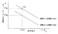
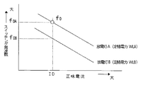
ここで、図3に示した基準電圧とスイッチング周波数との関係を表す特性図を用いて、上記した基準電圧とスイッチング周波数の関係から装着された放電灯5cの定格値を識別する方法について詳しく説明する。なお、図中、横軸は基準電圧回路14から出力される基準電圧、縦軸はインバータ駆動回路3のスイッチング周波数であり、放電灯Aおよび放電灯Bで表す線は、それぞれ、異なる定格電力WLAおよびWLB(WLA>WLB)を有する2種類の放電灯の特性曲線である。
【0032】
上記したように、この放電灯点灯装置では、積分回路8からの出力が基準電圧回路14から出力される基準電圧に等しくなるよう、誤差増幅器9がインバータ駆動回路3のスイッチング周波数を制御するため、基準電圧回路14から出力される基準電圧が定められると、定常状態においては、この基準電圧に対応する正味電流およびこの正味電流を供給しうるスイッチング周波数が一義的に決定される。こうして、同一の放電灯に対して、基準電圧を変更すれば、これに伴って、スイッチング周波数と正味電流が変化し、図3に示したような特性曲線を得ることができる。
【0033】
一方、結合コンデンサ4と放電灯負荷回路5からなる回路系はLCRから成る共振系を構成しているため、定格値の異なる放電灯を装着した場合、放電灯5cのインピーダンスの違いに起因して同一正味電流(すなわち、基準電圧)を供給できるスイッチング周波数が変化し、それぞれ、異なる特性曲線を有することになる。例えば、図3に示す例では、定格電力がWLA>WLBである放電灯AおよびBを同一の基準電圧(VREF)で駆動した場合、定格電力が大なる放電灯Aのスイッチング周波数fDAが、定格電力が小なる放電灯Bのスイッチング周波数fDBより大きくなり、こうして、基準電圧を最も小さい正味電流を与える基準電圧に一定に保った状態で放電灯点灯装置を運転しながら、周波数検出手段21から出力された信号をA/D変換してスイッチング周波数fDを検出し、この周波数がこの基準電圧(VREF)に対応した各放電灯のスイッチング周波数fDAおよびfDBのどちらにより近いかを比較することにより、装着された放電灯5cの定格値を識別することができる。
【0034】
なお、この図3では、基準電圧とスイッチング周波数との関係を特性曲線として表現したが、実際の放電灯点灯装置では、起動時の基準電圧(VREF)が定まっているため、設定された基準電圧に対応するスイッチング周波数fDAおよびfDBのみを記憶回路22bに保存しておき、周波数検出手段21から出力されたスイッチング周波数をこの値と比較するだけで定格値の識別ができ、この場合、基準電圧を検知する手段も不要である。
【0035】
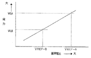
また、図4には、誤差増幅器9に入力される基準電圧と放電灯負荷回路5で消費される電力の関係を表す特性図を示す。定格値に適合した基準電圧が選択された後、新たに設定された基準電圧と電流検出回路6の出力電圧が等しくなるよう誤差増幅器9およびインバータ駆動回路3によりスイッチング周波数が制御され、直流電源1から放電灯5cの定格値に適合した高周波電流(正味電流)が放電灯負荷回路5に供給されて、回路損失を無視すれば、この正味電流に対応した一定の電力(図3の例では、WLA)が放電灯5cで消費される。
【0036】
以上、この実施の形態1によれば、放電灯負荷回路5に供給される正味電流を基準電圧回路14から出力される基準電圧によって制御するよう構成するとともに、所定の基準電圧で運転した時、すなわち、所定の正味電流が供給されている時のインバータ回路2のスイッチング周波数fDを周波数検出手段21によって検出することにより、放電灯負荷回路5に装着されている放電灯5cの定格値をスイッチ制御部22で識別して、スイッチ部20で基準電圧回路14から出力される基準電圧を自動的に切り替え、装着された放電灯5cの定格値に適合した正味電流を放電灯負荷回路5に供給するよう構成したため、同一の放電灯点灯装置で種々の定格値を有する放電灯に適用可能な放電灯点灯装置を得ることができ、この結果、多種類の部品や放電灯点灯装置を備える必要がなくなり、生産時の部品管理等の管理コストが安くなる効果がある。また、放電灯5cの定格値に合わせて自動的に基準電圧が変更されるため、製品出荷時等にスイッチを操作して手動で定格値を設定する必要がないといった利点もある。
【0037】
また、放電灯点灯装置を設置した後に照度アップなどのために放電灯5cの定格値を変更する場合も、放電灯5cの定格値に合わせて基準電圧が自動的に切り替わるため、同一の放電灯点灯装置で異なる定格値の放電灯を使用することができ、放電灯点灯装置を新たに交換、設置する必要がなくなって、購入費用や放電灯点灯装置の交換のための運用コストが削減できるとともに、長期にわたって使用可能な資源効率に優れた放電灯点灯装置が得られる効果がある。
【0038】
さらに、スイッチ制御部22およびスイッチ部20からなる基準電圧選択手段23が、装着されている放電灯5cの定格値を判断し、基準電圧を自動的に切り替えて放電灯5cの定格値に適合した正味電流を供給するよう構成したため、電気の知識がなくても放電灯5cの定格値に適合した正味電流を流すことができ、放電灯5cの交換時等において、放電灯5cの選択ミスやスイッチの設定ミス等により放電灯5cに過大な電流を印加して放電灯5cが短寿命となることを防止できる効果がある。
【0039】
また、基準電圧回路14を、基準電圧用直流電源11と分割抵抗12a、12b、12cおよび13とを備え、あらかじめ設定された放電灯の定格値に対応した複数の異なる基準電圧を生成する基準電圧発生部15と、基準電圧発生部15で生成した基準電圧を自動的に選択する基準電圧選択手段23とで構成したため、回路構成がシンプルになり、安価な基準電圧回路が得られる効果があるとともに、例えば、分割抵抗12を可変抵抗等によって構成し、可変抵抗の抵抗を変えて電圧の分割比を変更する方式に比べて、基準電圧の設定が容易となる効果がある。
【0040】
また、スイッチ制御部22を、A/D変換器22a、記憶回路22bおよび演算回路22cとから構成し、A/D変換器22aで電流検出回路6の出力をデジタルデータ化するとともに、演算回路22cにおいて、このデジタルデータを記憶回路22bにあらかじめ保存された周波数データと比較して装着された放電灯5cの定格値を識別し、基準電圧回路14からこの定格値に対応した基準電圧が出力されるようスイッチ部20に制御信号を出力するよう構成したため、記憶回路22b内のデータを変更するだけで多種類の放電灯に対応でき、適用範囲の広い柔軟性に優れた放電灯点灯装置が得られる効果がある。
【0041】
また、スイッチ制御部22をマイコンで、また、スイッチ部20を半導体スイッチで構成したため、基準電圧選択手段23の回路を集積化でき、装置の小型化が可能となる効果がある。
【0042】
さらに、この実施の形態1では、放電灯点灯装置の起動時に出力される基準電圧を、最も小さい正味電流に対応した基準電圧に設定したため、定格値の小さな放電灯に過大な電流を流して放電灯5cが短寿命となることを防止できる効果がある。
【0043】
また、周波数検出手段として、インバータ駆動回路3内の周波数出力端子21aからスイッチング周波数の信号を得るよう構成したため、応答が速く、正確なスイッチング周波数が得られる効果がある。
【0044】
なお、この実施の形態1においては、放電灯負荷回路5に供給される正味電流およびスイッチング周波数が定常状態になるまで、一定時間待機してからスイッチング周波数を検出するよう構成した例を示したが、起動時から周波数検出手段21およびスイッチ制御部22でスイッチング周波数を繰り返し検知し、スイッチング周波数が一定となったところで定常状態になったものと判断して、放電灯5cの定格値を識別するようにしてもよく、この場合、定常状態になるまでの裕度をもっておく必要がないため、速やかに定格値の変更ができる効果がある。
【0045】
また、上記では、スイッチ20aをONにした状態でスイッチング周波数を検出する場合について説明したが、その他のスイッチをONにした状態で起動して周波数を検出してもよく、さらには、記憶回路21bに図3のような特性曲線が保存されている場合は、任意のスイッチをONにして起動し、演算回路21cによってスイッチ部20の設定状況を検知し、この設定状況に対応した基準電圧とスイッチング周波数から放電灯5cの定格値を識別するよう構成してもよい。
【0046】
また、基準電圧選択手段23として、スイッチ制御部22をマイコンで、また、スイッチ部20を半導体スイッチで構成した例を示したが、例えば、異なる電圧でON、OFFされるリレーを組み合わせ、周波数検出手段21からの出力電圧によって各スイッチ20a、20b、20cの接点がON/OFFされるリレー回路で構成し、アナログ処理してもよく、また、上記したように、分割抵抗12として可変抵抗を用いて、電圧の分割比を変更するよう構成してもよい。
【0047】
さらに、上記図1では、周波数検出手段21として、スイッチング周波数をインバータ駆動回路3の周波数出力端子21aから検出するよう構成した例を示したが、例えば、インバータ回路2や放電灯負荷回路5等に流れる電流または電圧波形をスイッチ制御部22に入力し、スイッチ制御部22内のA/D変換器22aでデジタルデータ化した後、演算回路21cでフーリエ変換してスイッチング周波数を検出するよう構成してもよい。
【0048】
また、この実施の形態1では、インバータ駆動回路3を電圧制御発振回路3aとドライバ3bで構成した例を示したが、電圧制御発振回路3aの替りに電流制御発振回路を応用しても良く、上記と全く同様の効果が得られる。
【0049】
実施の形態2.
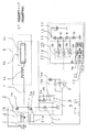
図5には、この発明の実施の形態2である放電灯点灯装置の構成を表す回路図を示す。この実施の形態2では、インバータ駆動回路3は、電流によって発振周波数が制御される電流制御発振回路3c(図中、「CCO」と記載)とドライバ3bから構成されるとともに、インバータ駆動回路3とグランド間には抵抗24が、また、インバータ駆動回路3と誤差増幅器9間にはダイオード25が接続されている。また、基準電圧回路14内のスイッチ制御部22には、インバータ駆動回路3の周波数出力端子21aから接続線21bを介してスイッチング周波数が、さらに、電流検出回路6からは接続線26を介して放電灯負荷回路5に供給される正味電流に対応した出力が入力されている。なお、図中、図1と同一または相当部分は同一記号を付し、説明を省略する。
【0050】
以下、この実施の形態2の動作について、電圧制御発振回路3aと電流制御発振回路3cの動作の違い、および、電流検出回路6から出力される正味電流データの利用方法を中心に説明する。図5は、この実施の形態2の構成を表す回路図であり、図において、電流制御発振回路3cは、電流制御発振回路3cの内部に内蔵された内部電源(図示せず)から流れ出る電流値によって発振周波数が制御される発振回路であり、この例では、内部電源から抵抗24を介してグランドに流れ出る電流とダイオード25から誤差増幅器9に引き込まれる電流の合計電流によって電流制御発振回路3cの発振周波数が制御される。
【0051】
まず、この放電灯点灯装置の起動時に、スイッチ制御部22によって、スイッチ部20のスイッチ20a、20b、20cのうち最も小さい正味電流に対応したスイッチ20aをONに、また、他のスイッチ20b、20cをOFFに設定しておく。この状態で、放電灯点灯装置を動作させると、電流制御発信回路3cの内部電源(図示せず)から、抵抗24を通ってグランドに電流が流れるとともに、抵抗24の上流側に比べて誤差増幅器9側の電位が低いためダイオード25を通って誤差増幅器9側にも電流が流入する。こうして、電流制御発信回路3cは、内部電源から抵抗24を介してグランドに流れ出る電流とダイオード25から誤差増幅器9に引き込まれる電流の合計電流に対応した発振周波数で発振し、この信号をドライバ3bで増幅して、インバータ回路2を駆動することにより、直流電源1から供給される直流電流が高周波電流に変換されて、放電灯負荷回路5に供給され、放電灯5cが点灯する。
【0052】
一方、放電灯負荷回路5に電流が流れ出すと、検出抵抗7には図12と同様の交流電流が流れ、積分回路8でこの交流電流の順方向および逆方向の電流の和(正味電流)が検出されて誤差増幅器9の反転入力端に入力され、非反転入力端に入力された基準電圧との差が誤差増幅器9で増幅されて出力されることにより、ダイオード25の下流側の電位が変化し、この結果、電流制御発振回路3cから誤差増幅器9側へ流出する電流量が変化して、電流制御発振回路3cの発振周波数が制御され、電流検出回路6からの出力が基準電圧に等しくなるまでスイッチング周波数が制御されて、定常状態に移行する。
【0053】
こうして、この実施の形態2においても、スイッチ部20により最も小さい正味電流に対応した基準電圧が選択されると、誤差増幅器9がインバータ駆動回路3のスイッチング周波数を制御して、放電灯負荷回路5に供給される正味電流が選択された基準電圧に対応した電流値となるよう調整され、定常状態においては、実施の形態1と同様に基準電圧と正味電流およびスイッチング周波数が一義的に対応することとなり、図3と同様の基準電圧とスイッチング周波数の関係を記憶回路22bに保存しておけば、周波数検出手段21によって検出されたスイッチング周波数から装着された放電灯5cの定格値が識別でき、演算回路22cとスイッチ部20によりこの定格値に適合した基準電圧への切り替えを自動的に行うことができる。
【0054】
しかしながら、この実施の形態2では、以下のような構成と動作により一層精密に定格値の識別が行えるよう構成している。すなわち、上記したように、この実施の形態2では、電流制御発振回路3cが抵抗24および誤差増幅器9へ流出する合計電流によって制御されるため、基準電圧回路14から出力される基準電圧を設定しても抵抗24の抵抗値にばらつきがあると、電流制御発振回路3cから流出する電流値が変化し、この結果、所定の基準電圧に対応したインバータ回路3のスイッチング周波数にばらつきが生じて、定格値を精密に識別することが困難になる。
【0055】
そこで、この実施の形態2では、基準電圧とスイッチング周波数の関係からではなく、図6に例示したような正味電流値とスイッチング周波数の関係から放電灯5cの定格値を直接識別するよう構成している。具体的には、周波数検出手段21からのスイッチング周波数の信号と電流検出回路6からの正味電流の信号をスイッチ制御部22に入力し、スイッチ制御部22のA/D変換器22aでスイッチング周波数と正味電流値を検出するとともに、記憶回路22bに保存された正味電流値とスイッチング周波数のデータから放電灯5cの定格値を直接識別し、演算回路22cとスイッチ部20によりこの定格値に適合した基準電圧への切り替えを自動的に行うのである。
【0056】
上記したように、定常状態においては基準電圧と正味電流およびスイッチング周波数が1対1の関係にあるため、正味電流とスイッチング周波数の関係からも放電灯5cの定格値を識別することが可能であり、特に、正味電流値とスイッチング周波数の関係は、インバータ回路2および放電灯負荷回路5の特性のみによって決定されるため、このような識別方法を採用すれば、抵抗24のばらつき等に影響されずに、常に放電灯5cの定格値を精密に識別できるようになる。
【0057】
以上のように、この実施の形態2によれば、上記の実施の形態1と全く同様の効果が得られるとともに、電流検出回路6から出力される正味電流のデータと周波数検出手段21からのスイッチング周波数のデータから放電灯5cの定格値を直接識別し、基準電圧を選択するよう構成したため、抵抗24のばらつき等に影響されずに一層精密に定格値を識別できる効果がある。
【0058】
なお、上記の説明から明らかなように、この実施の形態2の電流制御発振回路3cを電圧制御発振回路で構成しても、正味電流とスイッチング周波数の関係から定格値を識別するよう構成することにより、全く同様の効果が得られる。また、上記の実施の形態2では、正味電流の値を得る方法として、電流検出回路6から誤差増幅器9へ出力される信号を分岐してスイッチ制御部22に入力した例を示したが、上記の電流検出回路6とは別に電流検出回路を設けてスイッチ制御部22に入力するよう構成してもよい。
【0059】
さらに、上記図5では、スイッチング周波数をインバータ駆動回路3の周波数出力端子21aから検出するよう構成した例を示したが、電流検出回路6から出力される正味電流の信号が完全に平滑化されておらず、スイッチング周波数成分が含まれている場合は、この信号をA/D変換器22aでデジタル化した後、演算回路21cでフーリエ変換してスイッチング周波数を検出してもよく、この場合、周波数出力端子21aへの接続等が不要となって、回路が簡単になる効果がある。
【0060】
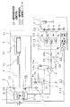
実施の形態3.
図7には、この発明の実施の形態3である放電灯点灯装置の回路図を示す。なお、この発明は、例えば、三菱電機オスラム株式会社製のHf蛍光放電灯(形名FHF32EX)のように、同一の放電灯で複数の定格値を有している(FHF32EXの場合は、32Wと45Wの2つの定格電力を有する)放電灯を、実施の形態1に示した放電灯点灯装置で駆動した場合、基準電圧VREFに対するスイッチング周波数fDを表す特性曲線が1本だけとなるため、スイッチ制御部22だけではこの放電灯5cを32Wで運転するのか、45Wで運転するかの識別ができないといった問題点を解決するためになされたものである。
【0061】
以下、この実施の形態3の構成および動作について図7を用いて説明する。図7において、27は、スイッチ制御部22に設けられた放電灯5cの定格を外部から手動で設定するための外部設定手段であり、この実施の形態では、「自動モード」、「32Wモード」、「45Wモード」の3つのモードが切り替えられる外部設定スイッチで構成されている。なお、図1と同一または相当部分は同一記号を付し、説明を省略する。
【0062】
以下、この実施の形態3の動作について説明する。図7において、この放電灯点灯装置が起動されると、まず、基準電圧回路14から最も小さい正味電流に対応した基準電圧が出力され、誤差増幅器9がインバータ駆動回路3に制御信号を送出してインバータ回路2のスイッチング周波数を制御し、電流検出回路6からの出力が基準電圧と等しくなるよう放電灯負荷回路5に供給される電流を調整する。一方、この基準電圧で運転されている間にスイッチ制御部22では、最初に、外部設定スイッチ27の設定状況が検出され、「自動モード」に設定されている場合は、実施の形態1と同様の手順で装着された放電灯5cの定格値が自動識別され、一定時間後に、この定格値に適合した基準電圧に切り替えられる。また、外部設定スイッチ27の設定が「32Wモード」あるいは「45Wモード」である場合は、自動識別を行わず、この外部設定スイッチ27で設定された定格値で放電灯5cを点灯するようスイッチ部20を切り替える。
【0063】
こうして、この実施の形態3によれば、上記した実施の形態1で得られた効果に加え、スイッチ制御部22に、定格値のマニュアル設定が可能な外部設定手段27を付加したため、同一放電灯で複数の定格値を有する放電灯に対しても対応できる放電灯点灯装置が得られる効果がある。
【0064】
なお、上記の実施の形態3では、まず、外部設定スイッチ27の設定状況を検出し、この設定状況によってスイッチ制御部22で「自動モード」、「32Wモード」、「45Wモード」の、それぞれに対応した処理を行うよう構成した例を示したが、複数の定格値を有する放電灯の基準電圧とスイッチング周波数の特性曲線が分かっている場合は、まず、起動時の基準電圧とスイッチング周波数の関係から複数定格を有する放電灯であるかどうかを判断し、複数定格である場合に、外部設定スイッチ27の設定状況を確認に行くよう構成してもよく、この場合、複数定格以外の放電灯に対しては上記の実施の形態1と同様にして定格値の自動識別が行われる。
【0065】
また、上記においては、外部設定スイッチ27として「自動モード」以外に、「32Wモード」、「45Wモード」の2つのモードを持つ例を示したが、外部設定スイッチ27の接点の数を増やせば、3つ以上の定格値にも対応できることは明らかである。
【0066】
実施の形態4.
図8には、この発明の実施の形態4として、基準電圧の切り替えに伴う放電灯5cの明るさの変化を連続的に変化させることが可能な放電灯点灯装置の回路図を示す。図において、28a、28bおよび29は、それぞれ、緩衝用抵抗、緩衝用コンデンサおよび抵抗であり、緩衝用抵抗28aと緩衝用コンデンサ28bは全体として緩衝用積分回路28を構成している。なお、図1と同一または相当部分は同一記号を付し、説明を省略する。
【0067】
このように、この実施の形態4では、基準電圧を選択するスイッチ部20のスイッチが、仮に、22aがONの状態から22bがONの状態に変化した場合に、その電圧の変化分が緩衝用積分回路28で積分されるので、誤差増幅器9に入力される基準電圧は緩衝用積分回路28の積分定数で連続的に変化し、この積分定数を適当に選定すれば、基準電圧の変化を徐々に変化させることができ、光出力をスム−スに変化させることができる。
【0068】
以上のように、この実施の形態4によれば、上記した実施の形態1で得られた効果に加え、誤差増幅器9の入力端と基準電圧回路14の間に緩衝回路28である緩衝用積分回路28を設け、基準電圧の切り替えにともなう基準電圧回路14の階段的な出力の変化を緩衝し、誤差増幅器9に入力される信号が徐々に、連続的に変化するよう構成したため、起動時の基準電圧から放電灯5cの定格値に適合した基準電圧に自動的に切り替える際等に生じる、放電灯5cの光出力(明るさ)の急激な階段状の変化を抑制することができ、起動から定常状態に至る光出力をスム−スに変化させることができるため、ユーザの違和感や不快感を減少でき、快適性に優れた放電灯点灯装置が得られる効果がある。
【0069】
なお、このように、毎起動時に放電灯5cの定格値が識別されスイッチ部20が切り替えられて基準電圧の選択が自動で行われる放電灯点灯装置においては、装置を起動するたびに放電灯5cの明るさが変化することになり、明るさが毎回急変することはユーザの快適性を大きく損なうもので、光出力をスム−スに変化させることのできる上記実施の形態4の放電灯点灯装置は実用上非常に大きな利点を有する。
【0070】
また、例えば、起動時の基準電圧から45W定格時に切り替える際も、直接45W定格の基準電圧に切り替えるのではなく、スイッチ制御部22で、32W→40W→45Wと順に1段づつ切り替えるようにすれば、緩衝用積分回路28の効果ともあいまって、光出力がより連続的に変化し、一層快適な放電灯点灯装置が得られる効果がある。
【0071】
さらに、上記の実施の形態4では、誤差増幅器9に入力される緩衝回路28として、緩衝用抵抗28aと緩衝用コンデンサ28bからなる緩衝用積分回路28を用いた例を示したが、例えば、オペアンプによる積分回路等の、これと同等の機能を持つ他の構成でも良い。
【0072】
実施の形態5.
図9には、実施の形態5である放電灯点灯装置の回路構成図を示す。これまでの実施の形態1ないし実施の形態4においては、スイッチ部20を基準電圧発生部15と誤差増幅器9の間に配置し、基準電圧発生部15により生成された複数の基準電圧の中から、スイッチ部20により誤差増幅器9に入力する基準電圧を選択するよう構成した例を示したが、図9に示すこの実施の形態のように、スイッチ部20の各スイッチ20a、20、20cを各分割抵抗12a、12b、12cに並列に接続し、スイッチ部20の各スイッチをON、OFFすることによって分割抵抗12a、12b、12cがバイパスされ、誤差増幅器9に接続された基準電圧の出力端の両側の分割抵抗の分割比が変化して、基準電圧が変更されるよう構成してもよい。
【0073】
なお、図9中、16は、分割抵抗12a、12b、12cおよび13に直列に接続された分割抵抗であり、また、図1と同一または相当部分は同一記号を付し、説明を省略する。さらに、動作についても、上記の実施の形態1と全く同様であり、説明を省略する。
【0074】
こうして、この実施の形態5によれば、上記した実施の形態1で得られた効果に加え、以下のような効果が得られる。すなわち、一般に誤差増幅器9の入力インピ−ダンスは非常に大きいことから、実施の形態1に示した例では、スイッチ部20の各接点には長期間にわたって微少電流が流れ続けることになり、このような条件下で基準電圧の値を長期間安定して保つことはなかなか困難であった。しかし、この実施の形態5によれば、スイッチ部20を分割抵抗12a、12b、12cに並列に接続したため、スイッチ部20には、基準電圧用直流電源11からの分割抵抗を流れる電流が流れることになり、経年変化に対して安定を保つために必要十分な電流値を流すことができるため、経年変化に対して耐久性が高く、信頼性の高い放電灯点灯装置が得られる効果がある。
【0075】
なお、図9では、スイッチ部20の各スイッチ20a、20b、20cを各分割抵抗12a、12b、12cの上流側とグランド間に並列に設けた例を示したが、スイッチ部20の各スイッチ20a、20b、20cが、それぞれ、分割抵抗12a、12b、12cをバイパスするよう接続しても良く、この場合、各スイッチの切り替えにより多種類の分割比を得ることができ、少ない分割抵抗数でより多くの定格値に対応できる放電灯点灯装置が得られる効果がある。
【0076】
実施の形態6.
また、上記の実施の形態1ないし実施の形態5において、基準電圧発生部15やスイッチ部20を含む基準電圧回路14を誤差増幅器9と同一の回路基板上に実装すれば、放電灯5cの放電によって基準電圧発生部15やスイッチ部20を流れる微少電流が外乱ノイズの影響で変動し、放電灯5cの出力が不安定になることを防止できるとともに、スイッチ部を別基板に設置する場合に比べてノイズ対策費用が軽減できる利点がある。
【0077】
実施の形態7.
さらに、回路基板を金属等で形成したケース内に収納すれば、放電灯5cの取り替え時等に回路基板を損傷する危険が少なくなり、また、ケースを金属で形成すれば放電灯5cの放電によるノイズの影響が一層軽減される効果もある。
【0078】
また、上記の実施の形態1ないし実施の形態5においては、誤差増幅器9に積分用のコンデンサ10bを付加した例を示したが、積分回路8の積分定数を適当に選定すれば、誤差増幅器9の積分の機能は不要となり、コンデンサ10bは増幅用の抵抗によって置き換えることができる。また、積分回路8の機能を誤差増幅器9内に一体化してもよい。
【0079】
さらに、上記の実施の形態1ないし実施の形態5では、誤差増幅器9に入力される基準電圧の数を3種類としたが、これを2種類または4種類以上としても全く同様の効果が得られる。また、放電灯負荷回路5として1灯用のものを例示したが、同一定格を持つ2灯用以上のものに適用しても良い。また、基準電圧用直流電源11を直流電源1から供給される直流電圧を一層安定化して使用するよう構成すれば、電源の共用が図られ、部品点数やコストが減少できる利点がある。
【0080】
さらに、上記の実施の形態1および実施の形態6では、それぞれ、基本的な構成のみを説明したが、これらの構成を組み合わせることにより一層使い易い放電灯点灯装置が得られることは明らかであり、また、インバ−タ駆動回路3内の発振回路を、電流制御発振回路(CCO)または電圧制御発振回路(VCO)のどちらで構成しても同様の効果が得られる。
【0081】
【発明の効果】
この発明は、以上説明したように構成されているので、以下に示すような効果を奏する。
【0082】
インバータ回路から放電灯負荷回路に供給される電流を基準電圧回路から出力される基準電圧によって制御するよう構成するとともに、上記インバータ回路のスイッチング周波数を検出する周波数検出手段を設け、基準電圧選択手段が、上記周波数検出手段によって検出されたスイッチング周波数から上記放電灯負荷回路に装着された放電灯の定格値を識別し、この定格値に対応した基準電圧を自動的に選択して上記基準電圧回路から出力するよう構成したため、同一の放電灯点灯装置で種々の定格値を有する放電灯に適用可能な放電灯点灯装置を得ることができ、この結果、生産時の部品管理等の管理コストが安くなる効果がある。また、放電灯の定格値に合わせて基準電圧が自動的に切り替わるため、放電灯の交換時等において放電灯の選択ミス等によって放電灯が短寿命となることを防止できる効果がある。
【0083】
また、上記放電灯負荷回路に供給される電流を検出する電流検出手段を設け、上記周波数検出手段から出力されるスイッチング周波数と上記放電灯負荷回路に供給される電流値から上記放電灯負荷回路に装着された放電灯の定格値を識別し、基準電圧選択手段でこの定格値に対応した基準電圧を自動的に選択して上記基準電圧回路から出力するよう構成したため、一層正確に定格値を識別できる効果がある。
【0084】
また、上記基準電圧回路を、基準電圧用直流電源と上記基準電圧用直流電源の電圧を分割する分割抵抗とを備え、あらかじめ設定された放電灯の定格値に対応した複数の異なる基準電圧を発生する基準電圧発生部と、上記周波数検出手段からの出力に基づいて上記放電灯負荷回路に装着された放電灯の定格値を識別し、上記基準電圧発生部で生成する基準電圧の中からこの定格値に適合した基準電圧を自動的に選択する基準電圧選択手段とから構成したため、上記基準電圧回路の構成がシンプルになり、安価な基準電圧回路が得られるとともに、基準電圧の設定が容易となる効果がある。
【0085】
また、上記基準電圧選択手段内のスイッチ部を上記分割抵抗に並列に接続したため、経年変化に対して安定した動作が得られ、信頼性の高い放電灯点灯装置が得られる効果がある。
【0086】
さらに、上記基準電圧選択手段内のスイッチ制御部を、A/D変換器と、記憶回路と、演算回路とから構成し、上記A/D変換器で上記周波数検出手段の出力をデジタルデータ化するとともに、上記演算回路において、上記記憶回路にあらかじめ保存された周波数データと比較して装着された放電灯の定格値を識別するよう構成したため、上記記憶回路内のデータを変更するだけで多種類の放電灯に対応でき、適用範囲の広い放電灯点灯装置が得られる効果がある。
【0087】
また、放電灯点灯装置の起動時に、上記基準電圧回路から出力可能な基準電圧のうち最も小さい正味電流に対応した基準電圧が上記基準電圧回路から出力されるよう構成したため、定格値の小さな放電灯に過大な電流を流して放電灯が短寿命となることを防止できる効果がある。
【0088】
また、放電灯の定格値を識別する情報を上記基準電圧選択手段に手動で入力できる外部設定手段を設けたため、複数の定格値を有する放電灯にも対応できる放電灯点灯装置が得られる効果がある。
【0089】
さらに、上記基準電圧回路と上記誤差増幅器との間に緩衝回路を設け、上記基準電圧回路から出力される基準電圧が変化する際、上記誤差増幅器に入力される基準電圧が連続的に変化するよう構成したため、基準電圧の切り替えに伴う放電灯の光出力(明るさ)の急激な変化を抑制することができ、起動から定常状態に至る光出力がスム−スに変化するため、ユーザの違和感や不快感を減少でき、快適性に優れた放電灯点灯装置が得られる効果がある。
【0090】
また、上記基準電圧回路を上記誤差増幅器が実装された回路基板上に設けたため、上記スイッチ部等を流れる微少電流が外乱ノイズの影響で変動して、放電灯の出力が不安定になることを防止できるとともに、別基板に設置する場合に比べてノイズ対策費用が軽減できる効果がある。
【0091】
また、上記基準電圧回路および上記誤差増幅器が実装された回路基板をケース内に収納したため、上記回路基板の損傷が防止される効果もある。
【図面の簡単な説明】
【図1】 この発明の実施の形態1の構成を示す回路図。
【図2】 この発明の実施の形態1の動作を示すフローチャート。
【図3】 この発明の実施の形態1の放電灯の定格値の識別方法を示す説明図。
【図4】 この発明の実施の形態1の基準電圧と消費電力の関係を表す特性図。
【図5】 この発明の実施の形態2の構成を示す回路図。
【図6】 この発明の実施の形態2の放電灯の定格値の識別方法を示す説明図。
【図7】 この発明の実施の形態3の構成を示す回路図。
【図8】 この発明の実施の形態4の構成を示す回路図。
【図9】 この発明の実施の形態5の構成を示す回路図。
【図10】 従来の放電灯点灯装置の構成を示す回路図。
【図11】 従来の放電灯点灯装置の直流電源の構成を示す回路図。
【図12】 従来の放電灯点灯装置の検出抵抗を流れる電流波形図。
【符号の説明】
1 直流電源
2 インバ−タ回路
3 インバータ駆動回路
5 放電灯負荷回路
5c 放電灯
6 電流検出回路
9 誤差増幅器
11 基準電圧用直流電源
12、12a、12b、12c 分割抵抗
13 分割抵抗
14 基準電圧回路
15 基準電圧発生部
16 分割抵抗
20 スイッチ部
20a、20b、20c スイッチ
21 周波数検出手段
22 スイッチ制御部
22a A/D変換器
22b 記憶回路
22c 演算回路
23 基準電圧選択手段
27 外部設定スイッチ(外部設定手段)
28 緩衝用積分回路(緩衝回路)[0001]
BACKGROUND OF THE INVENTION
The present invention relates to a discharge lamp lighting device that lights a discharge lamp with high-frequency power from an inverter circuit.
[0002]
[Prior art]
FIG. 10 shows a circuit diagram of a conventional discharge lamp lighting device. In the figure, 1 is a DC power source that rectifies and smoothes a commercial power source to obtain a DC current, 2 is an inverter circuit composed of
[0003]
Note that FIG. 11 shows a configuration example of the
[0004]
The operation of the conventional circuit shown in FIG. 10 will be described below. In the figure, when the
[0005]
On the other hand, the current detected by the
[0006]
[Problems to be solved by the invention]
However, in the conventional discharge lamp lighting device shown in FIG. 10 above, since the reference voltage output from the
[0007]
In addition, after installing the discharge lamp lighting device, when changing to a discharge lamp with a different rating value for the purpose of increasing the illuminance or saving power, it is necessary to replace and install the discharge lamp lighting device, which is a purchase cost. In addition, the operation cost required for replacing the discharge lamp lighting device is high.
[0008]
The present invention has been made to solve the above-described problems of the conventional apparatus, and a first object of the present invention is to automatically apply to a discharge lamp having a plurality of different rated values with one discharge lamp lighting apparatus. A discharge lamp lighting device that can automatically adapt to changes in the rated value of the discharge lamp even after installation, and that can reduce management costs such as parts management during production and operation costs after installation The purpose is to provide.
[0009]
Further, the second object of the present invention is to automatically change the rated value of the discharge lamp, so that the rated value can be easily changed, and even if there is no electrical knowledge, the rated value is ensured. An object of the present invention is to provide a discharge lamp lighting device that can be changed and that prevents a current exceeding the rated value from flowing through the discharge lamp even when the lamp is lit, so that the discharge lamp does not have a short life.
[0010]
A third object of the present invention is to provide a discharge lamp lighting device that can be adapted to a discharge lamp having a plurality of rated values with the same discharge lamp.
[0011]
Furthermore, a fourth object of the present invention is to provide a discharge lamp lighting device that suppresses a rapid change in brightness (light output) of a discharge lamp that accompanies a change in the rated value and is excellent in comfort during use. For the purpose.
[0012]
[Means for Solving the Problems]
In order to achieve the above object, a discharge lamp lighting device according to the present invention releases a direct current power source, an inverter circuit that converts a direct current supplied from the direct current power source into a high frequency current, and a high frequency current from the inverter circuit. A discharge lamp load circuit for lighting the lamp, a current detection circuit for detecting a current supplied from the inverter circuit to the discharge lamp load circuit, a reference voltage circuit for generating a reference voltage, and an output from the current detection circuit; An error amplifier that generates a control signal based on a reference voltage from the reference voltage circuit, and a switching frequency of the inverter circuit based on the control signal from the error amplifier, and the inverter circuit to the discharge lamp load circuit A discharge lamp lighting device comprising an inverter drive circuit for controlling a supplied current, the switch of the inverter circuit A frequency detecting means for detecting a switching frequency, and the reference voltage circuit is configured to output a plurality of different reference voltages corresponding to a rated value of the discharge lamp. Further, the reference voltage circuit includes the frequency detecting means. Provided with a reference voltage selection means for identifying the rated value of the discharge lamp mounted on the discharge lamp load circuit on the basis of the switching frequency detected by, and automatically selecting a reference voltage suitable for the rated value It is.
[0013]
Further, in the discharge lamp lighting device according to the present invention, the reference voltage selection means has a switching frequency output from the frequency detection means and a net current value supplied to the discharge lamp load circuit output from the current detection circuit. Based on the above, the rated value of the discharge lamp mounted on the discharge lamp load circuit is identified.
[0014]
Further, the discharge lamp lighting device according to the present invention includes the reference voltage circuit including a reference voltage DC power supply and a dividing resistor for dividing the voltage of the reference voltage DC power supply, and a preset rated value of the discharge lamp. A reference voltage generator for generating a plurality of different reference voltages corresponding to the reference voltage generator, and identifying a rated value of a discharge lamp mounted on the discharge lamp load circuit based on an output from the frequency detection means, and the reference voltage generator And a reference voltage selection means for automatically selecting a reference voltage that conforms to the rated value from the reference voltages generated in (1).
[0015]
The discharge lamp lighting device according to the present invention includes a reference voltage circuit, a reference voltage DC power supply, a dividing resistor that divides the voltage of the reference voltage DC power supply, a switch unit that selects a reference voltage, and the switch And a reference voltage selecting means including a switch control unit for controlling the unit, and connecting each switch of the switch unit in parallel to the dividing resistor and selecting a dividing resistor to be bypassed by the switch control unit Thus, the reference voltage output from the reference voltage circuit is selected.
[0016]
Furthermore, in the discharge lamp lighting device according to the present invention, the reference voltage selection means includes an A / D converter that converts the output of the frequency detection means into digital data, a storage circuit that stores the switching frequency of the inverter circuit, Comparing the digital data detected by the A / D converter with the switching frequency previously stored in the storage circuit, the rated value of the mounted discharge lamp is identified, and an arithmetic circuit for outputting a control signal is provided. And a switch unit that selects a reference voltage output from the reference voltage circuit in accordance with a control signal from the arithmetic circuit.
[0017]
In the discharge lamp lighting device according to the present invention, when the discharge lamp lighting device is started, the reference voltage selection unit selects a reference voltage corresponding to the smallest net current among the reference voltages that can be output from the reference voltage circuit. It is comprised so that it may do.
[0018]
Further, the discharge lamp lighting device according to the present invention is provided with external setting means that can manually input information for identifying the rated value of the discharge lamp to the reference voltage selection means.
[0019]
Furthermore, the discharge lamp lighting device according to the present invention is provided with a buffer circuit between the reference voltage circuit and the error amplifier, and is input to the error amplifier when the reference voltage output from the reference voltage circuit is changed. The reference voltage is configured to change continuously.
[0020]
In the discharge lamp lighting device according to the present invention, the reference voltage circuit is provided on a circuit board on which the error amplifier is mounted.
[0021]
The discharge lamp lighting device according to the present invention includes a circuit board on which the reference voltage circuit and the error amplifier are mounted in a case.
[0022]
DETAILED DESCRIPTION OF THE INVENTION
1 is a circuit diagram showing a configuration of a discharge lamp lighting device according to
[0023]
On the other hand, in the first embodiment, the
[0024]
Further, the
[0025]
Further, as shown in FIG. 1, the specific configuration of the
[0026]
The operation of the first embodiment will be described below with reference to the configuration diagram of FIG. 1 and the flowchart of FIG. First, in step S1, when the discharge lamp lighting device is activated, the
[0027]
At this time, since the
[0028]
On the other hand, the reference voltage is input from the
[0029]
Thus, in step S2, the discharge lamp lighting device is operated at a reference voltage corresponding to the minimum net current for a certain period of time after startup, and the net current supplied to the discharge
[0030]
Based on the identification result, a reference voltage that matches the rated value of the mounted
[0031]
Here, using the characteristic diagram showing the relationship between the reference voltage and the switching frequency shown in FIG. 3, a method for identifying the rated value of the mounted
[0032]
As described above, in this discharge lamp lighting device, since the
[0033]
On the other hand, since the circuit system composed of the
[0034]
In FIG. 3, the relationship between the reference voltage and the switching frequency is expressed as a characteristic curve. However, in an actual discharge lamp lighting device, since the reference voltage (VREF) at the time of starting is determined, the set reference voltage Only the switching frequencies fDA and fDB corresponding to are stored in the
[0035]
FIG. 4 is a characteristic diagram showing the relationship between the reference voltage input to the
[0036]
As described above, according to the first embodiment, the net current supplied to the discharge
[0037]
In addition, when the rated value of the
[0038]
Further, the reference voltage selection means 23 comprising the
[0039]
The
[0040]
The
[0041]
Further, since the
[0042]
Furthermore, in this
[0043]
Further, since the frequency detection means is configured to obtain a switching frequency signal from the
[0044]
In the first embodiment, an example is shown in which the switching frequency is detected after waiting for a certain time until the net current supplied to the discharge
[0045]
In the above description, the switching frequency is detected with the
[0046]
In addition, as an example of the reference
[0047]
Further, in FIG. 1, an example is shown in which the frequency detection means 21 is configured to detect the switching frequency from the
[0048]
In the first embodiment, the
[0049]
FIG. 5 is a circuit diagram showing a configuration of a discharge lamp lighting device according to
[0050]
Hereinafter, the operation of the second embodiment will be described focusing on the difference in operation between the voltage controlled oscillation circuit 3a and the current controlled oscillation circuit 3c and the method of using the net current data output from the
[0051]
First, when starting the discharge lamp lighting device, the
[0052]
On the other hand, when a current starts to flow into the discharge
[0053]
Thus, also in the second embodiment, when the reference voltage corresponding to the smallest net current is selected by the
[0054]
However, in the second embodiment, the rated value can be identified more precisely by the following configuration and operation. That is, as described above, in the second embodiment, since the current control oscillation circuit 3c is controlled by the total current flowing out to the
[0055]
Therefore, the second embodiment is configured to directly identify the rated value of the
[0056]
As described above, since the reference voltage, the net current, and the switching frequency are in a one-to-one relationship in the steady state, the rated value of the
[0057]
As described above, according to the second embodiment, the same effect as in the first embodiment can be obtained, and the data of the net current output from the
[0058]
As is apparent from the above description, even if the current controlled oscillation circuit 3c of the second embodiment is configured by a voltage controlled oscillation circuit, the rated value is identified from the relationship between the net current and the switching frequency. Thus, the same effect can be obtained. In the second embodiment, as an example of the method for obtaining the net current value, the signal output from the
[0059]
5 shows an example in which the switching frequency is detected from the
[0060]
FIG. 7 shows a circuit diagram of a discharge lamp lighting device according to
[0061]
The configuration and operation of the third embodiment will be described below with reference to FIG. In FIG. 7, reference numeral 27 denotes external setting means for manually setting the rating of the
[0062]
Hereinafter, the operation of the third embodiment will be described. In FIG. 7, when the discharge lamp lighting device is activated, first, a reference voltage corresponding to the smallest net current is output from the
[0063]
Thus, according to the third embodiment, in addition to the effect obtained in the first embodiment described above, the external setting means 27 capable of manually setting the rated value is added to the
[0064]
In the third embodiment, first, the setting state of the external setting switch 27 is detected, and the
[0065]
In the above, an example in which the external setting switch 27 has two modes of “32 W mode” and “45 W mode” in addition to the “automatic mode” has been shown. However, if the number of contacts of the external setting switch 27 is increased. It is clear that three or more rated values can be handled.
[0066]
FIG. 8 shows a circuit diagram of a discharge lamp lighting device capable of continuously changing the brightness change of the
[0067]
As described above, in the fourth embodiment, if the switch of the
[0068]
As described above, according to the fourth embodiment, in addition to the effect obtained in the first embodiment described above, the buffering integration which is the
[0069]
In this way, in the discharge lamp lighting device in which the rated value of the
[0070]
Also, for example, when switching from the reference voltage at startup to 45 W rating, instead of switching directly to the 45 W rated reference voltage, the
[0071]
Furthermore, in the above-described fourth embodiment, an example in which the
[0072]
In FIG. 9, the circuit block diagram of the discharge lamp lighting device which is
[0073]
In FIG. 9,
[0074]
Thus, according to the fifth embodiment, in addition to the effects obtained in the first embodiment, the following effects can be obtained. In other words, since the input impedance of the
[0075]
9 shows an example in which the
[0076]
In the first to fifth embodiments, if the
[0077]
Furthermore, if the circuit board is housed in a case formed of metal or the like, the risk of damaging the circuit board when the
[0078]
In the first to fifth embodiments, the example in which the integrating
[0079]
Furthermore, in the first to fifth embodiments described above, the number of reference voltages input to the
[0080]
Furthermore, in
[0081]
【The invention's effect】
Since the present invention is configured as described above, the following effects can be obtained.
[0082]
The current supplied from the inverter circuit to the discharge lamp load circuit is controlled by the reference voltage output from the reference voltage circuit, and frequency detection means for detecting the switching frequency of the inverter circuit is provided, and the reference voltage selection means is The rated value of the discharge lamp mounted on the discharge lamp load circuit is identified from the switching frequency detected by the frequency detecting means, and a reference voltage corresponding to the rated value is automatically selected from the reference voltage circuit. Since it is configured to output, it is possible to obtain a discharge lamp lighting device that can be applied to a discharge lamp having various rated values with the same discharge lamp lighting device, and as a result, the management cost of parts management and the like during production is reduced. effective. In addition, since the reference voltage is automatically switched in accordance with the rated value of the discharge lamp, there is an effect that it is possible to prevent the discharge lamp from having a short life due to a selection mistake of the discharge lamp when replacing the discharge lamp.
[0083]
Further, current detection means for detecting a current supplied to the discharge lamp load circuit is provided, and the discharge lamp load circuit is provided with a switching frequency output from the frequency detection means and a current value supplied to the discharge lamp load circuit. The rated value of the mounted discharge lamp is identified, and the reference voltage selection means automatically selects the reference voltage corresponding to this rated value and outputs it from the reference voltage circuit, so the rated value can be identified more accurately. There is an effect that can be done.
[0084]
The reference voltage circuit includes a reference voltage DC power supply and a dividing resistor for dividing the voltage of the reference voltage DC power supply, and generates a plurality of different reference voltages corresponding to preset rated values of the discharge lamp. A reference voltage generator for identifying the rated value of the discharge lamp mounted on the discharge lamp load circuit based on the output from the frequency detection means, and the rating is selected from the reference voltages generated by the reference voltage generator. Since the reference voltage selecting means that automatically selects a reference voltage suitable for the value is configured, the configuration of the reference voltage circuit is simplified, an inexpensive reference voltage circuit is obtained, and the setting of the reference voltage is facilitated. effective.
[0085]
Further, since the switch section in the reference voltage selection means is connected in parallel to the dividing resistor, it is possible to obtain a stable operation with respect to aging and to obtain a highly reliable discharge lamp lighting device.
[0086]
Further, the switch control unit in the reference voltage selection means is composed of an A / D converter, a storage circuit, and an arithmetic circuit, and the output of the frequency detection means is converted into digital data by the A / D converter. At the same time, the arithmetic circuit is configured to identify the rated value of the discharge lamp mounted in comparison with the frequency data stored in advance in the storage circuit, so that various types of data can be obtained simply by changing the data in the storage circuit. There is an effect that a discharge lamp lighting device that can deal with a discharge lamp and has a wide application range can be obtained.
[0087]
Further, since the reference voltage corresponding to the smallest net current among the reference voltages that can be output from the reference voltage circuit is output from the reference voltage circuit when the discharge lamp lighting device is started up, the discharge lamp having a small rated value is provided. Therefore, it is possible to prevent the discharge lamp from having a short life by passing an excessive current.
[0088]
Further, since the external setting means that can manually input information for identifying the rated value of the discharge lamp to the reference voltage selecting means is provided, there is an effect that a discharge lamp lighting device that can deal with a discharge lamp having a plurality of rated values can be obtained. is there.
[0089]
Further, a buffer circuit is provided between the reference voltage circuit and the error amplifier so that when the reference voltage output from the reference voltage circuit changes, the reference voltage input to the error amplifier continuously changes. As a result, the rapid change in the light output (brightness) of the discharge lamp associated with the switching of the reference voltage can be suppressed, and the light output from the start to the steady state changes smoothly. There is an effect that an unpleasant feeling can be reduced and a discharge lamp lighting device excellent in comfort can be obtained.
[0090]
In addition, since the reference voltage circuit is provided on the circuit board on which the error amplifier is mounted, a minute current flowing through the switch unit or the like fluctuates due to disturbance noise, and the output of the discharge lamp becomes unstable. In addition to preventing the noise, the noise countermeasure cost can be reduced as compared with the case where it is installed on a separate substrate.
[0091]
Further, since the circuit board on which the reference voltage circuit and the error amplifier are mounted is housed in the case, the circuit board is also prevented from being damaged.
[Brief description of the drawings]
FIG. 1 is a circuit diagram showing a configuration of a first embodiment of the present invention.
FIG. 2 is a flowchart showing the operation of the first embodiment of the present invention.
FIG. 3 is an explanatory diagram showing a method for identifying a rated value of a discharge lamp according to
FIG. 4 is a characteristic diagram showing a relationship between a reference voltage and power consumption according to the first embodiment of the present invention.
FIG. 5 is a circuit diagram showing a configuration of a second embodiment of the present invention.
FIG. 6 is an explanatory diagram showing a method for identifying a rated value of a discharge lamp according to a second embodiment of the present invention.
FIG. 7 is a circuit diagram showing a configuration of a third embodiment of the present invention.
FIG. 8 is a circuit diagram showing a configuration of a fourth embodiment of the present invention.
FIG. 9 is a circuit diagram showing a configuration of a fifth embodiment of the present invention.
FIG. 10 is a circuit diagram showing a configuration of a conventional discharge lamp lighting device.
FIG. 11 is a circuit diagram showing a configuration of a DC power source of a conventional discharge lamp lighting device.
FIG. 12 is a waveform diagram of current flowing through a detection resistor of a conventional discharge lamp lighting device.
[Explanation of symbols]
1 DC power supply
2 Inverter circuit
3 Inverter drive circuit
5 Discharge lamp load circuit
5c discharge lamp
6 Current detection circuit
9 Error amplifier
11 DC power supply for reference voltage
12, 12a, 12b, 12c Split resistor
13 Split resistor
14 Reference voltage circuit
15 Reference voltage generator
16 Split resistance
20 Switch part
20a, 20b, 20c switch
21 Frequency detection means
22 Switch controller
22a A / D converter
22b Memory circuit
22c arithmetic circuit
23 Reference voltage selection means
27 External setting switch (external setting means)
28 Buffer integration circuit (buffer circuit)
Claims (10)
Priority Applications (4)
| Application Number | Priority Date | Filing Date | Title |
|---|---|---|---|
| JP32163698A JP4040769B2 (en) | 1998-11-12 | 1998-11-12 | Discharge lamp lighting device |
| TW088117653A TW538654B (en) | 1998-10-19 | 1999-10-13 | Discharge lamp lighting device |
| EP99947921A EP1041862A4 (en) | 1998-10-19 | 1999-10-15 | IGNITION DEVICE FOR DISCHARGE LAMP |
| PCT/JP1999/005703 WO2000024230A1 (en) | 1998-10-19 | 1999-10-15 | Apparatus for lighting discharge lamp |
Applications Claiming Priority (1)
| Application Number | Priority Date | Filing Date | Title |
|---|---|---|---|
| JP32163698A JP4040769B2 (en) | 1998-11-12 | 1998-11-12 | Discharge lamp lighting device |
Publications (2)
| Publication Number | Publication Date |
|---|---|
| JP2000150185A JP2000150185A (en) | 2000-05-30 |
| JP4040769B2 true JP4040769B2 (en) | 2008-01-30 |
Family
ID=18134724
Family Applications (1)
| Application Number | Title | Priority Date | Filing Date |
|---|---|---|---|
| JP32163698A Expired - Fee Related JP4040769B2 (en) | 1998-10-19 | 1998-11-12 | Discharge lamp lighting device |
Country Status (1)
| Country | Link |
|---|---|
| JP (1) | JP4040769B2 (en) |
Families Citing this family (2)
| Publication number | Priority date | Publication date | Assignee | Title |
|---|---|---|---|---|
| JP2008234877A (en) * | 2007-03-16 | 2008-10-02 | Toshiba Lighting & Technology Corp | Discharge lamp lighting device |
| EP3219010B1 (en) * | 2014-11-11 | 2020-07-08 | Maschinenfabrik Reinhausen GmbH | Resistor emulation and gate boost |
-
1998
- 1998-11-12 JP JP32163698A patent/JP4040769B2/en not_active Expired - Fee Related
Also Published As
| Publication number | Publication date |
|---|---|
| JP2000150185A (en) | 2000-05-30 |
Similar Documents
| Publication | Publication Date | Title |
|---|---|---|
| US10277133B2 (en) | Isolated DC/DC converter, primary side controller, power adapter, and electronic device | |
| JP2010140675A (en) | Power supply device | |
| US7336057B2 (en) | DC/DC converter | |
| JP4352460B2 (en) | Power supply | |
| JP4040769B2 (en) | Discharge lamp lighting device | |
| US6111763A (en) | Switching power supply | |
| JP4083895B2 (en) | Discharge lamp lighting device | |
| EP1041862A1 (en) | Apparatus for lighting discharge lamp | |
| KR102490634B1 (en) | A Converter Circuit for LED Lamps Having Power Factor Correction Function with Dimming and Overheat-Preventng Function | |
| JP2004127907A (en) | Lighting system | |
| JP4524924B2 (en) | Discharge lamp lighting device | |
| JPH1141914A (en) | DC-DC converter | |
| JPH06251890A (en) | Dimming device in discharge lamp lighting device | |
| JP2007200621A (en) | Discharge lamp lighting device and lighting device | |
| JP4272870B2 (en) | Switching regulator | |
| KR100565590B1 (en) | Power circuit | |
| JP2005183114A (en) | Discharge lamp lighting device and luminaire equipped therewith | |
| JP2004355859A (en) | Lighting device for discharge lamp | |
| JP2000012269A (en) | Discharge lamp lighting device | |
| JP2003068487A (en) | Lighting device of discharge lamp | |
| JPH118084A (en) | Discharge lamp lighting device | |
| JPH10271848A (en) | Power device | |
| JP2008034148A (en) | Discharge lamp lighting device and luminaire | |
| JP2004040965A (en) | Power supply device | |
| KR20050066433A (en) | (a) circuit for driving a load |
Legal Events
| Date | Code | Title | Description |
|---|---|---|---|
| RD01 | Notification of change of attorney |
Free format text: JAPANESE INTERMEDIATE CODE: A7421 Effective date: 20040810 |
|
| A621 | Written request for application examination |
Free format text: JAPANESE INTERMEDIATE CODE: A621 Effective date: 20051026 |
|
| TRDD | Decision of grant or rejection written | ||
| A01 | Written decision to grant a patent or to grant a registration (utility model) |
Free format text: JAPANESE INTERMEDIATE CODE: A01 Effective date: 20071030 |
|
| A61 | First payment of annual fees (during grant procedure) |
Free format text: JAPANESE INTERMEDIATE CODE: A61 Effective date: 20071108 |
|
| FPAY | Renewal fee payment (event date is renewal date of database) |
Free format text: PAYMENT UNTIL: 20101116 Year of fee payment: 3 |
|
| R150 | Certificate of patent or registration of utility model |
Free format text: JAPANESE INTERMEDIATE CODE: R150 |
|
| FPAY | Renewal fee payment (event date is renewal date of database) |
Free format text: PAYMENT UNTIL: 20111116 Year of fee payment: 4 |
|
| FPAY | Renewal fee payment (event date is renewal date of database) |
Free format text: PAYMENT UNTIL: 20121116 Year of fee payment: 5 |
|
| FPAY | Renewal fee payment (event date is renewal date of database) |
Free format text: PAYMENT UNTIL: 20121116 Year of fee payment: 5 |
|
| FPAY | Renewal fee payment (event date is renewal date of database) |
Free format text: PAYMENT UNTIL: 20131116 Year of fee payment: 6 |
|
| R250 | Receipt of annual fees |
Free format text: JAPANESE INTERMEDIATE CODE: R250 |
|
| LAPS | Cancellation because of no payment of annual fees |