JP4520593B2 - Green luminescent SrAl12O19 luminescent material activated with Mn2 + - Google Patents
Green luminescent SrAl12O19 luminescent material activated with Mn2 + Download PDFInfo
- Publication number
- JP4520593B2 JP4520593B2 JP2000224692A JP2000224692A JP4520593B2 JP 4520593 B2 JP4520593 B2 JP 4520593B2 JP 2000224692 A JP2000224692 A JP 2000224692A JP 2000224692 A JP2000224692 A JP 2000224692A JP 4520593 B2 JP4520593 B2 JP 4520593B2
- Authority
- JP
- Japan
- Prior art keywords
- phosphor
- ions
- formula
- light
- composition
- Prior art date
- Legal status (The legal status is an assumption and is not a legal conclusion. Google has not performed a legal analysis and makes no representation as to the accuracy of the status listed.)
- Expired - Fee Related
Links
Images


Classifications
-
- H—ELECTRICITY
- H01—ELECTRIC ELEMENTS
- H01J—ELECTRIC DISCHARGE TUBES OR DISCHARGE LAMPS
- H01J61/00—Gas-discharge or vapour-discharge lamps
- H01J61/02—Details
- H01J61/38—Devices for influencing the colour or wavelength of the light
- H01J61/42—Devices for influencing the colour or wavelength of the light by transforming the wavelength of the light by luminescence
- H01J61/44—Devices characterised by the luminescent material
-
- C—CHEMISTRY; METALLURGY
- C09—DYES; PAINTS; POLISHES; NATURAL RESINS; ADHESIVES; COMPOSITIONS NOT OTHERWISE PROVIDED FOR; APPLICATIONS OF MATERIALS NOT OTHERWISE PROVIDED FOR
- C09K—MATERIALS FOR MISCELLANEOUS APPLICATIONS, NOT PROVIDED FOR ELSEWHERE
- C09K11/00—Luminescent, e.g. electroluminescent, chemiluminescent materials
- C09K11/08—Luminescent, e.g. electroluminescent, chemiluminescent materials containing inorganic luminescent materials
- C09K11/77—Luminescent, e.g. electroluminescent, chemiluminescent materials containing inorganic luminescent materials containing rare earth metals
- C09K11/7701—Chalogenides
- C09K11/7703—Chalogenides with alkaline earth metals
-
- C—CHEMISTRY; METALLURGY
- C09—DYES; PAINTS; POLISHES; NATURAL RESINS; ADHESIVES; COMPOSITIONS NOT OTHERWISE PROVIDED FOR; APPLICATIONS OF MATERIALS NOT OTHERWISE PROVIDED FOR
- C09K—MATERIALS FOR MISCELLANEOUS APPLICATIONS, NOT PROVIDED FOR ELSEWHERE
- C09K11/00—Luminescent, e.g. electroluminescent, chemiluminescent materials
- C09K11/08—Luminescent, e.g. electroluminescent, chemiluminescent materials containing inorganic luminescent materials
- C09K11/77—Luminescent, e.g. electroluminescent, chemiluminescent materials containing inorganic luminescent materials containing rare earth metals
- C09K11/7712—Borates
-
- C—CHEMISTRY; METALLURGY
- C09—DYES; PAINTS; POLISHES; NATURAL RESINS; ADHESIVES; COMPOSITIONS NOT OTHERWISE PROVIDED FOR; APPLICATIONS OF MATERIALS NOT OTHERWISE PROVIDED FOR
- C09K—MATERIALS FOR MISCELLANEOUS APPLICATIONS, NOT PROVIDED FOR ELSEWHERE
- C09K11/00—Luminescent, e.g. electroluminescent, chemiluminescent materials
- C09K11/08—Luminescent, e.g. electroluminescent, chemiluminescent materials containing inorganic luminescent materials
- C09K11/77—Luminescent, e.g. electroluminescent, chemiluminescent materials containing inorganic luminescent materials containing rare earth metals
- C09K11/7766—Luminescent, e.g. electroluminescent, chemiluminescent materials containing inorganic luminescent materials containing rare earth metals containing two or more rare earth metals
- C09K11/7774—Aluminates
-
- H—ELECTRICITY
- H01—ELECTRIC ELEMENTS
- H01J—ELECTRIC DISCHARGE TUBES OR DISCHARGE LAMPS
- H01J29/00—Details of cathode-ray tubes or of electron-beam tubes of the types covered by group H01J31/00
- H01J29/02—Electrodes; Screens; Mounting, supporting, spacing or insulating thereof
- H01J29/10—Screens on or from which an image or pattern is formed, picked up, converted or stored
- H01J29/18—Luminescent screens
- H01J29/20—Luminescent screens characterised by the luminescent material
-
- G—PHYSICS
- G21—NUCLEAR PHYSICS; NUCLEAR ENGINEERING
- G21K—TECHNIQUES FOR HANDLING PARTICLES OR IONISING RADIATION NOT OTHERWISE PROVIDED FOR; IRRADIATION DEVICES; GAMMA RAY OR X-RAY MICROSCOPES
- G21K4/00—Conversion screens for the conversion of the spatial distribution of X-rays or particle radiation into visible images, e.g. fluoroscopic screens
- G21K2004/06—Conversion screens for the conversion of the spatial distribution of X-rays or particle radiation into visible images, e.g. fluoroscopic screens with a phosphor layer
Landscapes
- Chemical & Material Sciences (AREA)
- Inorganic Chemistry (AREA)
- Engineering & Computer Science (AREA)
- Materials Engineering (AREA)
- Organic Chemistry (AREA)
- Luminescent Compositions (AREA)
- Measurement Of Radiation (AREA)
- Inorganic Compounds Of Heavy Metals (AREA)
- Compounds Of Alkaline-Earth Elements, Aluminum Or Rare-Earth Metals (AREA)
- Crystals, And After-Treatments Of Crystals (AREA)
- Gas-Filled Discharge Tubes (AREA)
Description
【0001】
【発明の分野】
本発明は各種のイオンが添加された発光材料に関するものであって、更に詳しく言えば、Mn2+、Ce3+、Pr3+、Gd3+、Tb3+及び(又は)Mg2+が添加されかつランプ蛍光体、ディスプレイ蛍光体又はレーザ結晶として使用されるSrAl12O19に関する。
【0002】
【発明の背景】
発光材料は電磁スペクトルの一部分におけるエネルギーを吸収し、そして電磁スペクトルの別の部分におけるエネルギーを放出する。粉末状の発光材料は一般に蛍光体と呼ばれるのに対し、透明な固体状の発光材料は一般にシンチレータと呼ばれる。
【0003】
有用な蛍光体及びシンチレータの大部分は、スペクトルの可視域外の放射の吸収に応答してスペクトルの可視域内の放射を放出する。すなわち、蛍光体は人間の目が感じない電磁放射を人間の目が感じる電磁放射に変換する機能を果たす。ほとんどの蛍光体は、電磁スペクトルの可視域よりも高エネルギーの領域に対して応答する。すなわち、(蛍光ランプの場合のように)紫外線、(陰極線管の場合のように)電子、及び(放射線写真の場合のように)X線に対して応答性を示す蛍光体及びシンチレータが存在する。
【0004】
大別して、2種の発光材料が認められている。それらは、自己賦活発光材料及び不純物賦活発光材料である。
【0005】
自己賦活発光材料とは、純粋な結晶性ホスト材料が高エネルギー光子を吸収して電子を励起状態に高めた後、それらの電子が光子を放出しながら低エネルギー状態に戻るようなものである。自己賦活発光材料は、励起状態又は低エネルギー状態において電子が有し得るエネルギーの範囲が比較的大きいため、幅の広い発光スペクトルを有するのが普通である。すなわち、ある励起電子が励起状態から低エネルギー状態に遷移する際には、それの発光遷移の前後においてそれが有する特定のエネルギーに応じてかなり広い範囲のエネルギーが放出されることがある。
【0006】
不純物賦活発光材料は、通常、非発光性のホスト材料が賦活剤化学種の含有により変性されて成るものである。かかる賦活剤化学種は、約200〜1000ppmの範囲内の比較的低い濃度でホスト材料中に存在する。しかるに、ある種の材料は最適化された光出力を得るために数モル%又は数原子%の活性化イオンを要求する。不純物賦活発光材料の場合、賦活剤イオンが入射光子を直接に吸収することもあれば、格子が入射光子を吸収し、次いで吸収された光子エネルギーを賦活剤イオンに伝達することもある。
【0007】
格子によって吸収された光子は、格子中に移動性の電子及び正孔を生み出すことがある。好ましい電荷配置のため、かかる移動性の電子及び正孔は賦活剤イオンにおいて捕捉される。その結果、それらは再結合してルミネセンス光の光子を放出する。
【0008】
あるいはまた、光子が賦活剤イオンによって直接に吸収される場合には、かかる光子は賦活剤イオンの1個以上の電子をより高い励起状態に持ち上げる。これらの電子は、より低い励起状態に戻る際にルミネセンス光の光子を放出する。
【0009】
多くの常用されている不純物賦活発光材料においては、ルミネセンス光を放出する電子はd殻又はf殻の電子である。それらのエネルギーレベルは、周囲の結晶場によってそれぞれ顕著な影響を受ける場合と、割合に影響を受けない場合とがある。賦活剤イオンが局所結晶場によってあまり影響を受けないような状況下では、放出されるルミネセンス光はホスト材料ではなく実質的に賦活剤イオンの特性を示すものであって、ルミネセンススペクトルは1つ以上の比較的幅の狭い発光ピークから成っている。これは、自己賦活発光材料が示す幅の広い発光スペクトルと対照的である。
【0010】
ホスト格子が入射光子(すなわち、励起エネルギー)を吸収し、そしてそれを賦活剤イオンに伝達する場合には、ホスト格子は増感剤として働く。かかるホスト格子にはまた、増感剤原子を添加することもできる。かかる増感剤原子は入射光子を直接に吸収するか、あるいはホスト格子から吸収し、そしてそれを賦活剤イオンに伝達する。
【0011】
緑色の光を放出する従来の蛍光体の一例はZn2SiO4:Mn2+である。この蛍光体は、プラズマディスプレイや陰極線管(CRT)のごときディスプレイ装置及び各種の蛍光ランプにおいて使用されている。この蛍光体は、ランプ又はプラズマディスプレイから放出された紫外線あるいはCRTにおける電子を吸収し、そして緑色スペクトル域内の光を放出する。
【0012】
蛍光体が放射線損傷に耐えて高いルーメン保持性を示すことは、一般に有利なことである。放射線損傷は、所定の強さの刺激放射線に応答して発光材料から放出される光の量が高い放射線量への暴露後に減少するような発光材料の特性である。ルーメン保持性は、発光材料が長時間にわたって放射線損傷に耐える能力である。長時間にわたって放射線損傷に対する高い抵抗性を示す発光材料は、高いルーメン保持性を有するわけである。
【0013】
しかるに、Zn2SiO4:Mn2+蛍光体は数百時間にわたる高エネルギー紫外線又は電子の衝撃を受けた後には光出力の顕著な減少を示した。それ故、この蛍光体は低いルーメン保持性を有することになる。
【0014】
最近、本発明者等のうちの2名は米国特許第5571451号において新規なSr1-xPrxAl12-yMgyO19 蛍光体を提唱した。この蛍光体は、Pr3+賦活剤からの発光に基づいて青色スペクトル域内の光を放出する。更にまた、この蛍光体はPrの量子分裂効果のために青色スペクトル域内において高い量子効率を示す。しかしながら、この蛍光体は緑色スペクトル域内においてルミネセンスを示さない。
【0015】
上記の事実に鑑みて、十分なルーメン保持性を示す緑色発光性蛍光体又はシンチレータ材料を提供することは望ましいわけである。また、かかる蛍光体又はシンチレータの方法を提供することも望ましいものである。
【0016】
【発明の概要】
本発明の実施の一態様に従えば、式
AD12O19:Mn,R
(式中、Aはストロンチウム、バリウム及びカルシウムのうちの少なくとも1種から成り、Dはアルミニウム、ガリウム、ホウ素及びマグネシウムのうちの少なくとも1種から成り、そしてRは少なくとも1種の3価希土類イオンから成る)によって表わされる組成物(composition of matter) が提供される。
【0017】
本発明の別の実施の態様に従えば、ハウジング、該ハウジング内に収容されたエネルギー媒体供給源、及び該ハウジングの内部に収容された発光材料を含む発光装置が提供される。上記の発光材料は、式
AD12O19:Mn,R
(式中、Aはストロンチウム、バリウム及びカルシウムのうちの少なくとも1種から成り、Dはアルミニウム、ガリウム、ホウ素及びマグネシウムのうちの少なくとも1種から成り、そしてRは少なくとも1種の3価希土類イオンから成る)によって表わされるものである。
【0018】
更にまた、本発明の実施の一態様に従えば、ストロンチウム、アルミニウム、マンガン、並びにガリウム、マグネシウム、ホウ素、カルシウム、バリウム、セリウム、プラセオジム、ガドリニウム及びテルビウムのうちの少なくとも1種の元素の酸化物、炭酸塩、水酸化物、硝酸塩又はシュウ酸塩を混合する工程と、こうして得られた混合物を加熱して蛍光体を生成させる工程とを含むような蛍光体の製造方法が提供される。また、本発明の実施の一態様に従えば、ストロンチウム、アルミニウム、酸素、マンガン、並びにガリウム、マグネシウム、ホウ素、カルシウム、バリウム、セリウム、プラセオジム、ガドリニウム及びテルビウムのうちの少なくとも1種から成る融液に接触させて単結晶の種晶を配置する工程と、種晶を高温域から低温域に移動させる工程と、種晶に接触した状態で単結晶シンチレータを生成させる工程とを含むようなシンチレータの製造方法が提供される。
【0019】
【好適な実施の態様の詳細な説明】
本発明者等は、Mn2+賦活剤イオンを添加した場合にSrAl12O19が緑色スペクトル域内の発光材料となることを発見した。更にまた、Ce、Pr、Gd及びTbのごとき3価希土類イオンはSrAl12O19:Mn2+中において増感剤として働く。この材料は、飽和度の高い緑色ルミネセンス(すなわち、緑色スペクトル域内に最大波長を有する鋭い発光ピーク)を有すると共に、緑色−黄色スペクトル域内に幅の広い発光ピークを有する従来のZn2SiO4:Mn2+に比べて同等の絶対量子効率を有している。SrAl12O19:Mn2+蛍光体はまた、それのマグネトプランバイト型格子構造が本質的に安定であるため、高エネルギー放射線損傷抵抗性及びルーメン保持性の点でもZn2SiO4:Mn2+蛍光体より優れている。
【0020】
本発明者等はMn及び3価希土類イオンの添加がSrAl12O19から緑色発光を生み出す理由に関して特定の理論により束縛されることを望まないが、本発明者等は次のように考えている。
【0021】
SrAl12O19材料は、図1に示されるごとく、マグネトプランバイト型構造を成して結晶化する。Mn2+ドーパントイオンは、鏡映面を占めないAlの四面体状陽イオン部位にあるAlイオンを置換する。各々のMnイオンは4つの結合を有するから、それらのMnイオンは四面体状に配位している。四面体状に配位したMn2+イオンは、弱い結晶場の作用を受ける。それ故、SrAl12O19:Mn2+は緑色スペクトル域内において光を放出する。なぜなら、ルミネセンスによって放出される光は実質的にホスト材料ではなくMn2+賦活剤イオンに固有のものだからである。
【0022】
ストロンチウムイオンは、マグネトプランバイト型格子の鏡映面内の陽イオン部位を占める。それ故、これらのイオンは格子の鏡映面を拡大し、そして格子中における結晶場効果の源となる。3価希土類ドーパントイオンは、Sr格子部位を占める。希土類イオンはSrイオンより大きいから、希土類イオンはSrイオンより多量の鏡映面拡大を引起こすことがあり、従ってMn2+賦活剤イオンに対する増感剤として働く。
【0023】
好適な3価希土類イオンは、セリウム(Ce)、プラセオジム(Pr)、ガドリニウム(Gd)及びテルビウム(Tb)である。とは言え、その他の3価希土類イオンを使用することもできる。本発明者等は、それぞれの希土類イオンが相異なる増感剤機能を有するものと考えている。Prは、185nmの入射光に対する増感剤として働く。それ故、発光材料に185nmの光が照射された場合、Sr格子部位にあるPrイオンは入射光を吸収し、そして入射光により発生されたエネルギーをAl部位のMn2+賦活剤イオンに伝達する。それ故、SrAl12O19:Mn2+が185nmで発光するUV気体放電ランプ用の緑色発光蛍光体として使用される場合、その蛍光体にはPr賦活剤イオンを添加すべきである。
【0024】
Ceは、254nmの入射光に対する増感剤として働く。それ故、発光材料に254nmの光が照射された場合、Sr格子部位にあるCeイオンは入射光を吸収し、そして入射光により発生されたエネルギーをAl部位のMn2+賦活剤イオンに伝達する。それ故、SrAl12O19:Mn2+が254nmで発光するUV気体放電ランプ用の緑色発光蛍光体として使用される場合、その蛍光体にはCe賦活剤イオンを添加すべきである。また、SrAl12O19:Mn2+が185nm及び254nmの両方で発光するランプ又はその他の光源用の緑色発光蛍光体として使用される場合には、Ce及びPr増感剤の両者を使用すべきである。なお、Pr及びCeはちょうど185nm及び254nmの波長に対してではなく約300nmにまで広がる相異なる波長範囲に対する増感剤として働くことに注意すべきである。
【0025】
本発明者等は、Gdイオンを利用する次のようなエネルギー伝達機構の可能性を考えている。Gdイオンは、SrAl12O19のマグネトプランバイト型格子中の互いに隣接したSr部位に存在してGdイオン部分格子を形成する。Pr又はCe増感剤は入射光を吸収し、そしてそのエネルギーを部分格子中の少なくとも1個のGdイオンに伝達する。次に、そのGdイオンは部分格子中の別のGdイオンにエネルギーを伝達する。やがて、そのエネルギーはMn2+賦活剤に隣接したGdイオンに到達する。すると、エネルギーは部分格子から賦活剤に伝達される。このように、Gdイオン部分格子は賦活剤イオンへのエネルギー伝達を容易にする。それ故、SrAl12O19:Mn2+にはPr及び(又は)Ceに加えてGdを添加することができる。
【0026】
Tbは、SrAl12O19:Mn2+中において量子効率増強剤として働く。本発明者等は、SrAl12O19:Mn2+にTbイオンを添加した場合、Tbイオンを添加しないSrAl12O19:Mn2+に比べて緑色のMn2+量子効率が改善されることを見い出した。それ故、SrAl12O19:Mn2+にはPr、Ce及び(又は)Gdイオンに加えてTbイオンを添加することができる。本発明者等は、改善された量子効率を達成するためSrAl12O19:Mn2+にTbイオン及びその他の3価希土類イオンを添加した場合、恐らくは複雑な多段エネルギー伝達が起こるものと考えている。本発明者等によれば、SrAl12O19:Mn2+,Tb3+,Ce3+中において、緑色の光は主としてMn2+イオンから発生されるのであって、Ce3+又はTb3+イオンから発生されるのではないことが確認された。
【0027】
少なくとも上記の理由から、SrAl12O19:Mn2+材料はそれの所要の用途に応じて1種、2種、3種又は4種の3価希土類イオンドーパント化学種の任意の組合せを含有し得る。なお、かかるドーパント化学種はPr、Ce、Gd及びTbから成ることが好ましい。
【0028】
更にまた、Alイオンの一部分をガリウム、ホウ素又はマグネシウムイオンドーパント化学種によって置換することもできる。Alイオンを置換するために好適なドーパント化学種はMgイオンである。Sr2+格子部位が3価希土類イオンで満たされた場合、Mgイオンは電荷補償イオンとして働く。所望ならば、Srイオンの一部分をカルシウム又はバリウムイオンドーパント化学種によって置換することもできる。
【0029】
それ故、本発明の実施の一態様に係わる発光材料は、下記の一般式
AD12O19:Mn,R
(式中、Aはストロンチウム、カルシウム及びバリウムのうちの少なくとも1種から成り、Dはアルミニウム、ガリウム、ホウ素及びマグネシウムのうちの少なくとも1種から成り、そしてRは少なくとも1種の3価希土類イオンから成る)によって特徴づけることができる。なお、Mnは+2価の原子価状態にある賦活剤イオンを成す。
【0030】
Mnイオン濃度は、D陽イオン化学種の1/12を基準として0モル%又は原子%を越えかつ50モル%又は原子%までの範囲内にあり得る。好適なMnイオン濃度範囲はD陽イオン化学種の1/12を基準として20〜30原子%であり、また好適なMnイオン濃度は25原子%である。換言すれば、全部で12モル又はイオンのD陽イオン化学種のうちに0〜0.5モル又はイオンのMnが存在し得るのである。D陽イオン化学種の残りの11.5〜12モルはAl又はAlとMgとの組合せから成り得る。
【0031】
マグネシウムイオン濃度は、全Alイオン濃度の1/12を基準として0〜50モル%又は原子%の範囲内にあり得る。好適なMgイオン濃度範囲はAl陽イオン化学種の1/12を基準として20〜30原子%であり、また好適なMgイオン濃度は25原子%である。換言すれば、全部で12モル又はイオンのD陽イオン化学種のうちに0〜0.5モル又はイオンのMgが存在し得るのである。
【0032】
Rイオン濃度は、A陽イオン化学種(すなわち、所望ならばカルシウム又はバリウム陽イオン化学種によって部分的に置換され得るストロンチウム陽イオン化学種)を基準として0モル%又は原子%を越えかつ100モル%又は原子%までの範囲内にあり得る。好適なRイオン濃度範囲はA陽イオン化学種を基準として25〜75原子%であり、また好適なRイオン濃度は50原子%である。
【0033】
Mn及びRイオンの濃度は、下記の式
(A1-xRx)(D12-zMnz)O19
(式中、0<x≦1かつ0<z≦0.5である)によって表わすことができる。本発明のある好適な材料においては、Aはストロンチウムから成り、Dはアルミニウム及びマグネシウムのうちの少なくとも1種から成り、そしてRはセリウム、プラセオジム、ガドリニウム及びテルビウムのうちの少なくとも1種から成る。
【0034】
セリウム及びプラセオジムイオン濃度は、全Srイオン濃度を基準としてそれぞれ0〜100モル%又は原子%の範囲内にあり得る。なお、Ce及びPrイオン濃度のいかなる組合せもSrイオン濃度を基準として100モル%又は原子%を越えてはならないことを理解すべきである。好適なCe及びPrイオン濃度範囲はSr陽イオン化学種を基準としてそれぞれ10〜40原子%である。Prイオンを添加せずにCeイオンを添加する場合、好適なCeイオン濃度はSr陽イオン化学種を基準として30原子%である。Ceイオンを添加せずにPrイオンを添加する場合、好適なPrイオン濃度はSr陽イオン化学種を基準として30原子%である。Ce及びPrイオンの両者を添加する場合、好適なCe及びPrイオン濃度はSr陽イオン化学種を基準としてそれぞれ15原子%である。
【0035】
Gd及びTbイオン濃度は、全Srイオン濃度を基準としてそれぞれ0〜50モル%又は原子%の範囲内にあり得る。好適なGd及びTbイオン濃度範囲はSr陽イオン化学種を基準としてそれぞれ5〜15原子%であり、また好適なGd及びTbイオン濃度はSr陽イオン化学種を基準としてそれぞれ10原子%である。
【0036】
本発明の好適な材料中におけるMg、Ce、Pr、Gd及びTbイオンの濃度は、下記の式
(Sr1-m-q-r-tCemPrqGdrTbt)(Al12-e-gMgeMng)O19
(式中、0≦m≦1、0≦q≦1、0≦r≦0.5、0≦t≦0.5、0≦e≦0.5、かつ0<g≦0.5である)によって表わすことができる。本発明のある好適な材料は、Mg、Ce、Pr、Gd及びTbイオンをゼロでない濃度で含有している。本発明の別の好適な材料は、Ce及びPrイオンのうちの少なくとも1種をゼロでない濃度で含有している。本発明の別の好適な材料は、Ce並びにGd及びTbイオンのうちの少なくとも1種をゼロでない濃度で含有している。本発明の更に別の好適な材料は、Pr並びにGd及びTbイオンのうちの少なくとも1種をゼロでない濃度で含有している。本発明に係わる3種の特定の好適な材料を挙げれば、
1: (Sr0.5Ce0.3Gd0.1Tb0.1)(Al11.5Mg0.25Mn0.25)O19
2: (Sr0.5Ce0.15Pr0.15Gd0.1Tb0.1)(Al11.5Mg0.25Mn0.25)O19
3: (Sr0.5Ce0.15Pr0.15Gd0.1Tb0.1)(Al11.75Mn0.25)O19
である。
【0037】
上記のごとき発光材料は、多種多様の用途において使用することができる。たとえば、かかる材料はランプ、陰極線管、プラズマディスプレイ装置又は液晶ディスプレイにおける蛍光体として使用することができる。かかる材料はまた、電磁熱量計、ガンマ線カメラ、計算機断層撮影スキャナ又はレーザにおけるシンチレータとして使用することもできる。これらの用途は例示的なものに過ぎないのであって、全てを尽くしていると解すべきではない。
【0038】
AD12O19:Mn,R蛍光体は、ランプにおいて使用することができる。たとえば、この蛍光体はたとえば図2に示されるような直管形蛍光ランプにおいて使用することができる。蛍光ランプは、ガスで満たされた管1、管1の内面上に形成された蛍光体2、複数の陰極又は気体放電電極3、及びランプキャップ又は口金4から成っている。あるいはまた、蛍光体2が管1の外面上に塗布される場合もあれば、ガスを含む独立の外被上に塗布される場合もある。管1はガラス製であることが好ましいが、その他適宜の透明な材料を使用することもできる。口金4を通して陰極3に電位が印加されると、水銀のごときガスは放射(すなわち、紫外線)を放出する。蛍光体2はガスからの入射紫外線を吸収し、そして緑色の光を放出する。
【0039】
AD12O19:Mn,R蛍光体はまた、陰極線管(CRT)においても使用することができる。たとえば、この蛍光体はたとえば図3に示されるようなテレビ受像機用として設計されたCRTにおいて使用することができる。かかるCRTは、少なくとも1個(好ましくは3個)の電子銃5、少なくとも1個の電子ビーム偏向装置6、陽極7、表示スクリーン10、及びスクリーンの内側に塗布された蛍光体2を含んでいる。かかるCRTの動作に際しては、電子銃5から電子ビーム8が放出される。電子ビーム8は陽極7によって蛍光体2に向けて引き寄せられる。蛍光体2上における電子ビーム8の位置は偏向装置6によって制御される。入射した電子ビーム8を吸収した部分の蛍光体2は、スクリーン10を通して緑色の光9を放出する。あるいはまた、CRTがたとえば図4に示されるごとく陰極アレイを含んでいてもよい。この場合、CRTはスピント型陰極11のアレイ(図示を明快にするために1個の陰極のみを示す)を含んでいる。制御回路(図示せず)が特定の陰極11に電位を印加すると、それは蛍光体2に向けて電子ビーム8を放出する。蛍光体2は電子ビーム8を緑色の光9に変換して放出する。
【0040】
AD12O19:Mn,R蛍光体はまた、たとえば図5に示されるような液晶ディスプレイ(LCD)においても使用することができる。かかるLCDは、透明な基板12、光源13、薄膜トランジスタのごとき複数の制御用トランジスタ14及び15のアレイ(図示を明快にするために2個のみを示す)、それぞれのトランジスタと電気的に接触した透明な電極16及び17、液晶材料18、透明な対向基板19、電極16の上方の対向基板19上に形成された蛍光体2、電極17の上方の対向基板19上に形成された別の蛍光体20、透明な表示スクリーン21、並びに不透明なハウジング22から成っている。トランジスタ14がオン状態になると、電極16がそれの直上の液晶材料18に電位を印加する。印加された電位は、電極16の上方の液晶材料18を透明にする。トランジスタ15から電極17に電位が印加されなければ、電極17の上方の液晶材料は不透明なままである。その時、ランプ13からの光は液晶材料18の透明な部分を通過して蛍光体2に到達することができる。蛍光体2はランプ13からの光を吸収し、そしてスクリーン21を通して緑色の光を放出する。液晶材料を通して様々な色の蛍光体2及び20に入射するランプ13からの光の透過状態を制御することにより、スクリーン21上に画像を形成することができる。蛍光体2はまた、対向基板19の上方に形成することもできるし、あるいはスクリーン21の内面上に形成することもできる。
【0041】
AD12O19:Mn,R蛍光体はまた、たとえば図6に示されるようなプラズマディスプレイ装置においても使用することができる。かかるプラズマディスプレイ装置は、透明な表示スクリーン21、不透明なハウジング22、ガス外被23、気体放電電極24のアレイ(図示を明快にするために1個の電極のみを示す)、及びトランジスタのごとき制御装置から成っている。蛍光体2は、ガス外被23の内面又は外面上に形成することもできるし、あるいはスクリーン21の内面上に形成することもできる。制御装置25が電極24に電位を印加すると、電極24は外被23の内部に収容されたガス中において局所プラズマ放電を引起こす。かかる局所プラズマから放出された紫外線は、蛍光体2の隣接部分によって吸収される。すると、蛍光体2の被照射部分がスクリーン21を通して緑色の光を放出する。電極アレイ中の様々な電極24に対する電位の印加状態を制御することにより、スクリーン21上に画像を形成することができる。
【0042】
本発明のシンチレータは、たとえば図7に示されるような計算機断層撮影(CT)スキャナシステムにおいて使用することができる。かかるスキャナシステムは、人体の断面像を得るために使用される。CTスキャナシステムにおいては、X線管41のごときX線源が患者43の回りに円を描きながら回転する。患者43の反対側にはX線検出器42が配置されている。検出器42は、X線源と同期しながら円の外周に沿って回転する。かかる検出器は、ホトダイオード又はその他の種類の光検出器に対して光学的に結合されたAD12O19:Mn,R蛍光体を含んでいる。あるいはまた、検出器42は透明な基板上に塗布されかつホトダイオード又はその他の種類の光検出器に対して光学的に結合されたAD12O19:Mn,R蛍光体を含んでいてもよい。
【0043】
AD12O19:Mn,Rシンチレータはまた、たとえば図8に示されるようなレーザ結晶を成すこともできる。かかるレーザは、ハウジング51、シンチレータ結晶52、及びランプ53のごとき光源から成っている。電圧源54から電極を通して結晶52に電位が印加される。結晶52が光源53によって照射されかつ電圧源54から電位が印加される限り、結晶52は窓55を通してコヒーレントな緑色光を放出する。所望に応じ、かかるレーザは全反射鏡56及び半透明鏡57を含むこともできる。これらの鏡は、両者間における光の往復反射によってコヒーレント光の振幅を増幅するために役立つ。あるいはまた、レーザ結晶52の劈開及び(又は)加工により、結晶の背面に全反射鏡面を形成すると共に、窓55に面した結晶52の前面に部分反射鏡面を形成することもできる。
【0044】
AD12O19:Mn,Rシンチレータはまた、ガンマ線カメラ又は電磁熱量計において使用することもできる。ガンマ線カメラにおいては、シンチレータはガンマ線を吸収して緑色の光を放出することによってフィルムを感光させる。電磁熱量計においては、シンチレータは高エネルギーの入射放射線(たとえば、望遠鏡によって集められたガンマ線又は陽電子源から放出された陽電子)を吸収して緑色の光を放出する。遠隔の放射線源からの入射放射線は、ハウジングに設けられた窓を通ってハウジング内に進入する。これらの用途においては、このような窓はシンチレータに対する入射放射線の供給源と見なすことができる。勿論、AD12O19:Mn,R蛍光体及びシンチレータは上記以外の用途においても使用することができる。
【0045】
AD12O19:Mn,R蛍光体は、液相(フラックス)法又は固体法のごとき任意のセラミック粉末法によって製造することができる。なお、かかる蛍光体の製造方法は次のような工程から成ることが好ましい。第一に、蛍光体原料を成す化合物がるつぼ又はその他の適当な容器(たとえば、ボールミル)内において混合される。たとえば、ZrO2 又はイットリウム強化ジルコニア製の摩砕媒体を含むボールミルを用いて出発原料を混合すればよい。好適な出発原料を成す化合物としては、金属成分の酸化物、炭酸塩、水酸化物、硝酸塩又はシュウ酸塩が挙げられる。たとえば、 (Sr1-m-q-r-tCemPrqGdrTbt)(Al12-e-gMgeMng)O19を生成するためには、炭酸ストロンチウム(SrCO3 )、酸化アルミニウム(アルミナ、Al2O3)又は水酸化アルミニウム(Al(OH)3 )、酸化プラセオジム(Pr6O11)、酸化セリウム(Ce2O)、酸化ガドリニウム(Gd2O3)、酸化テルビウム(Tb4O7)、炭酸マグネシウム(MgCO3 )、又は酸化マグネシウム(MgO)、及び酸化マンガン又は炭酸マンガン(MnCO3 )をるつぼ又はボールミル内において混合すればよい。
【0046】
次いで、混合した原料を還元雰囲気中において1400〜1600℃で5〜15時間(好ましくは1500℃で10時間)にわたり焼成することによって原料が焼結される。還元雰囲気は、生成ガス(2%の水素及び98%の窒素から成るガス)であり得る。出発原料はまた、セラミック蛍光体を生成するための焼成工程において出発原料の反応を促進するフラックスをも含有することが好ましい。かかるフラックスは、フッ化物又は塩化物のごときハロゲン化合物から成ることが好ましい。好適なハロゲン化合物としては、フッ化マグネシウム、アルミニウム又はストロンチウム、あるいは塩化マグネシウム、ストロンチウム、マンガン又はアンモニウムが挙げられる。とは言え、フラックスを添加せずに蛍光体を焼成することもできる。次いで、焼成済みの混合物を用いて表示スクリーン又はランプ管球のごとき基体が被覆される。なお、混合物粒子及び液体から成る懸濁液を用いて基体を被覆することが好ましい。
【0047】
AD12O19:Mn,Rシンチレータは、任意の結晶成長法によって製造することができる。なお、かかるシンチレータはブリッジマン−ストックバーガー(Bridgeman-Stockbarger) 法又はチョクラルスキー(Czochralski) 法によって製造することが好ましい。ブリッジマン−ストックバーガー結晶成長法の略図を図9に示す。固体のAD12O19:Mn,R材料が、単結晶の種晶61に接触した状態で外被又は容器内に配置される。種晶61はAD12O19:Mn,Rから成っていてもよいし、あるいはマグネトプランバイト型結晶構造を有する別の材料から成っていてもよい。次いで、固体材料が高温域62内に導入される。かかる高温域は抵抗加熱ヒータ又はランプヒータから成り得る。かかるヒータは固体材料の一部分のみを融解する棒形又はストリップ形のものであってもよいし、あるいは固体材料全体を融解して融液領域64を形成する炉であってもよい。次いで、種晶61及び融液領域64が低温域63内に移動させられる。高温域62が棒形ヒータから成る場合、低温域63はヒータから遠く離れた領域から成る。高温域62が炉から成る場合、低温域63は炉の外側の領域から成るか、あるいは第1の炉より低い温度に設定された第2の炉から成り得る。かかる2つの炉は、断熱材65によって隔離されていることが好ましい。融液領域64が低温域に到達すると、それは種晶61と同じ格子及び方位を有する単結晶66として凝固する。種晶及び固体材料は、静止したヒータ又は炉に対して移動させることができる。あるいはまた、静止した種晶61に対してヒータ又は炉を移動させることもできる。かかる相対運動は、鉛直方向、水平方向又はその他任意の方向に沿って行わせることができる。
【0048】
チョクラルスキー結晶成長法の略図を図10に示す。ストロンチウム、アルミニウム、酸素、並びにマグネシウム、マンガン、ガリウム、ホウ素、バリウム、カルシウム、セリウム、プラセオジム、ガドリニウム及びテルビウムのうちの少なくとも1種から成る出発原料をるつぼ71内に配置して加熱することにより、反応体融液72が生成される。るつぼは石英管73のごとき外被の内部に配置され、そして高周波ヒータ又は抵抗加熱ヒータ74によって加熱される。融液温度は熱電対75によって測定される。種晶ホルダ77に取付けられた単結晶の種晶76が(高温域内にある)融液中に降下させられる。種晶76をそれの軸線の回りに回転させながら融液72から引上げると、種晶の下方には単結晶シンチレータボウル78が生成する。種晶76を融液72からヒータ74上方の低温域に向かって引上げるのに伴い、単結晶ボウル78の大きさは増大する。かかるボウルをスライスして研磨することにより、シンチレータ結晶が得られる。
【0049】
【実施例】
下記のごとき方法によって (Sr0.5Ce0.3Gd0.1Tb0.1)(Al11.5Mg0.25Mn0.25)O19 蛍光体を製造した。すなわち、化学量論的な量の酸化物及び炭酸塩出発原料(SrCO3、Gd2O3、CeO2、Tb4O7、Al2O3、MnCO3 及びMgO)を良く混合した後、僅かに還元性の雰囲気(97%のN2 及び2%のH2 から成る生成ガス)中において1000℃で5時間にわたり焼成した。同じ還元雰囲気中において室温まで冷却した後、部分反応材料を再粉砕した。再粉砕した材料を同じ雰囲気中で1550℃まで再加熱した。こうして得られた蛍光体は、短波長の紫外線で励起した場合に鮮緑色の発光を示した。なお、出発原料間の反応を促進するため、出発原料にフッ化アルミニウム又はマグネシウムのフラックスを添加することもできる。
【0050】
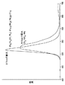
本発明の (Sr0.5Ce0.3Gd0.1Tb0.1)(Al11.5Mg0.25Mn0.25)O19 蛍光体及び従来のZn2SiO4:Mn2+蛍光体に254nmの入射光を照射し、そしてそれらの発光スペクトルを分光計で測定した。これらのスペクトルを図11に示す。 (Sr0.5Ce0.3Gd0.1Tb0.1)(Al11.5Mg0.25Mn0.25)O19 蛍光体は、517nmの最大発光波長を示した。緑色スペクトル域内にあるこの波長は、Zn2SiO4:Mn2+の最大発光波長である523nmから6nmしか離れていない。
【0051】
(Sr0.5Ce0.3Gd0.1Tb0.1)(Al11.5Mg0.25Mn0.25)O19蛍光体及び従来のZn2SiO4:Mn2+蛍光体の色度座標を下記表1中に記載すると共に、図12のCIE色度図中に示す。
【0052】
【表1】

色度座標x及びyは蛍光体業界において公知のものであって、たとえばケイ・エッチ・バトラー(K.H. Butler) の教科書「フルオレセント・ランプ・ホスファーズ・テクノロジー・アンド・セオリー(Fluorescent Lamp Phosphors, Technology and Theory) 」(ペンシルヴェニア州立大学出版局、1980年)の98〜107頁に定義されている。図中に実線で示された曲線は、特定のx及びy座標に対応する単色発光波長をを示している。図12からわかる通り、緑色域内にピーク発光波長を有する (Sr0.5Ce0.3Gd0.1Tb0.1)(Al11.5Mg0.25Mn0.25)O19 蛍光体(黒丸81)は、緑色−黄色域内にピーク発光波長を有する従来のZn2SiO4:Mn2+蛍光体(白丸82)よりも飽和度の高い緑色発光を示す。更にまた、これら2種の蛍光体は同等の絶対量子効率を有している。それ故、実質的に全ての用途においてZn2SiO4:Mn2+蛍光体の代りにAD12O19:Mn,R蛍光体を使用することができる。言うまでもないが、上記の実施例は本発明を例示するものに過ぎないのであって、本発明の範囲を制限するものと解すべきでない。
【0054】
以上、特定の実施の態様に関連して本発明を詳細に説明したが、本発明の精神及び範囲から逸脱することなしに様々な変更態様が可能であることは当業者にとって自明であろう。
【図面の簡単な説明】
【図1】マグネトプランバイト結晶構造の斜視図である。
【図2】本発明の実施の一態様に係わる蛍光体で被覆された陰極線管の側断面図である。
【図3】本発明の実施の一態様に係わる蛍光体で被覆された蛍光ランプの側断面図である。
【図4】本発明の実施の一態様に係わる蛍光体で被覆された蛍光ランプの側断面図である。
【図5】本発明の実施の一態様に係わる蛍光体で被覆された液晶ディスプレイ装置の側断面図である。
【図6】本発明の実施の一態様に係わる蛍光体で被覆されたプラズマディスプレイ装置の側断面図である。
【図7】本発明の実施の一態様に係わるシンチレータを含むX線検出装置の側断面図である。
【図8】本発明の実施の一態様に係わるシンチレータを含むレーザの側断面図である。
【図9】本発明の実施の一態様に係わるシンチレータの製造方法を示す略図である。
【図10】本発明の別の実施の態様に係わるシンチレータの製造方法を示す略図である。
【図11】254nmの入射光の下で、本発明の実施の一態様に係わる蛍光体の発光スペクトルと従来の蛍光体の発光スペクトルとを比較して示すグラフである。
【図12】本発明の実施の一態様に係わる蛍光体の色度座標と従来の蛍光体の色度座標を比較して示すグラフである。
【符号の説明】
1 管
2 蛍光体
3 陰極
4 口金
5 電子銃
6 電子ビーム偏向装置
7 陽極
8 電子ビーム
9 緑色の光
10 表示スクリーン
11 スピント型陰極
12 基板
13 光源又はランプ
14 制御用トランジスタ
15 制御用トランジスタ
16 電極
17 電極
18 液晶材料
19 対向基板
20 蛍光体
21 表示スクリーン
22 ハウジング
23 ガス外被
24 気体放電電極
25 制御装置
41 X線管
42 X線検出器
43 患者
51 ハウジング
52 シンチレータ結晶
53 ランプ
54 電圧源
55 窓
56 全反射鏡
57 半透明鏡[0001]
FIELD OF THE INVENTION
The present invention relates to a light-emitting material to which various ions are added.2+, Ce3+, Pr3+, Gd3+, Tb3+And / or Mg2+Added and used as lamp phosphor, display phosphor or laser crystal SrAl12O19About.
[0002]
BACKGROUND OF THE INVENTION
The luminescent material absorbs energy in one part of the electromagnetic spectrum and emits energy in another part of the electromagnetic spectrum. A powdery luminescent material is generally called a phosphor, whereas a transparent solid luminescent material is generally called a scintillator.
[0003]
Most useful phosphors and scintillators emit radiation in the visible region of the spectrum in response to absorption of radiation outside the visible region of the spectrum. In other words, the phosphor functions to convert electromagnetic radiation that the human eye does not feel into electromagnetic radiation that the human eye feels. Most phosphors respond to regions of higher energy than the visible region of the electromagnetic spectrum. That is, there are phosphors and scintillators that are responsive to ultraviolet light (as in the case of fluorescent lamps), electrons (as in the case of cathode ray tubes) and X-rays (as in the case of radiographs). .
[0004]
Broadly speaking, two types of luminescent materials are recognized. They are self-activated luminescent materials and impurity-activated luminescent materials.
[0005]
A self-activated luminescent material is one in which a pure crystalline host material absorbs high energy photons to raise electrons to an excited state and then returns to a low energy state while emitting them. Self-activated luminescent materials typically have a broad emission spectrum because the range of energy that electrons can have in an excited or low energy state is relatively large. That is, when a certain excited electron makes a transition from an excited state to a low energy state, a considerably wide range of energy may be emitted depending on the specific energy that it has before and after its emission transition.
[0006]
The impurity-activated luminescent material is usually formed by modifying a non-luminescent host material by containing an activator chemical species. Such activator species are present in the host material at a relatively low concentration in the range of about 200-1000 ppm. However, certain materials require several mole% or several atomic% of activated ions to obtain an optimized light output. In the case of impurity-activated luminescent materials, the activator ions may absorb incident photons directly, or the lattice may absorb incident photons and then transfer the absorbed photon energy to the activator ions.
[0007]
Photons absorbed by the lattice can create mobile electrons and holes in the lattice. Due to the preferred charge configuration, such mobile electrons and holes are trapped in the activator ions. As a result, they recombine and emit photons of luminescent light.
[0008]
Alternatively, if a photon is absorbed directly by the activator ion, such photon lifts one or more electrons of the activator ion to a higher excited state. These electrons emit photons of luminescent light as they return to a lower excited state.
[0009]
In many commonly used impurity-activated luminescent materials, the electrons emitting luminescence light are d-shell or f-shell electrons. Their energy level may be significantly affected by the surrounding crystal field, or may not be affected by the rate. In the situation where the activator ion is not significantly affected by the local crystal field, the emitted luminescence light is not a host material but is substantially characteristic of the activator ion, and the luminescence spectrum is 1 It consists of one or more relatively narrow emission peaks. This is in contrast to the broad emission spectrum exhibited by self-activated luminescent materials.
[0010]
If the host lattice absorbs incident photons (ie, excitation energy) and transmits it to activator ions, the host lattice acts as a sensitizer. Sensitizer atoms can also be added to such host lattices. Such sensitizer atoms either absorb incident photons directly or absorb from the host lattice and transmit it to activator ions.
[0011]
An example of a conventional phosphor that emits green light is Zn2SiOFour: Mn2+It is. This phosphor is used in a display device such as a plasma display or a cathode ray tube (CRT) and various fluorescent lamps. This phosphor absorbs ultraviolet or CRT electrons emitted from the lamp or plasma display and emits light in the green spectral range.
[0012]
It is generally advantageous for the phosphor to withstand radiation damage and exhibit high lumen retention. Radiation damage is a property of a luminescent material such that the amount of light emitted from the luminescent material in response to a predetermined intensity of stimulating radiation decreases after exposure to a high radiation dose. Lumen retention is the ability of a luminescent material to withstand radiation damage for extended periods of time. A luminescent material that exhibits high resistance to radiation damage over a long period of time has a high lumen retention.
[0013]
However, Zn2SiOFour: Mn2+The phosphor showed a significant decrease in light output after being subjected to high energy UV or electron bombardment for several hundred hours. Therefore, this phosphor has low lumen retention.
[0014]
Recently, two of the inventors have found a new Sr in US Pat. No. 5,571,451.1-xPrxAl12-yMgyO19A phosphor was proposed. This phosphor is composed of Pr3+Based on the light emission from the activator, it emits light in the blue spectral range. Furthermore, this phosphor exhibits high quantum efficiency in the blue spectral range due to the quantum splitting effect of Pr. However, this phosphor does not exhibit luminescence in the green spectral range.
[0015]
In view of the above facts, it would be desirable to provide a green emitting phosphor or scintillator material that exhibits sufficient lumen retention. It would also be desirable to provide such a phosphor or scintillator method.
[0016]
SUMMARY OF THE INVENTION
According to one embodiment of the present invention, the formula
AD12O19: Mn, R
Wherein A comprises at least one of strontium, barium and calcium, D comprises at least one of aluminum, gallium, boron and magnesium, and R comprises at least one trivalent rare earth ion. A composition of matter represented by) is provided.
[0017]
According to another embodiment of the present invention, a light emitting device is provided that includes a housing, an energy medium source housed within the housing, and a light emitting material housed within the housing. The above luminescent material
AD12O19: Mn, R
Wherein A comprises at least one of strontium, barium and calcium, D comprises at least one of aluminum, gallium, boron and magnesium, and R comprises at least one trivalent rare earth ion. It is represented by
[0018]
Furthermore, according to one embodiment of the present invention, strontium, aluminum, manganese, and an oxide of at least one element of gallium, magnesium, boron, calcium, barium, cerium, praseodymium, gadolinium, and terbium, There is provided a method for producing a phosphor including a step of mixing carbonate, hydroxide, nitrate, or oxalate, and a step of heating the mixture thus obtained to produce a phosphor. According to one embodiment of the present invention, a melt composed of strontium, aluminum, oxygen, manganese, and at least one of gallium, magnesium, boron, calcium, barium, cerium, praseodymium, gadolinium, and terbium is used. Manufacturing a scintillator including a step of placing a single crystal seed crystal in contact, a step of moving the seed crystal from a high temperature region to a low temperature region, and a step of generating a single crystal scintillator in contact with the seed crystal. A method is provided.
[0019]
DETAILED DESCRIPTION OF PREFERRED EMBODIMENTS
The present inventors have made Mn2+SrAl when activator ion is added12O19Has been found to be a luminescent material in the green spectral range. Furthermore, trivalent rare earth ions such as Ce, Pr, Gd and Tb are SrAl.12O19: Mn2+It works as a sensitizer inside. This material has a highly saturated green luminescence (ie, a sharp emission peak with a maximum wavelength in the green spectral range) and a conventional Zn with a broad emission peak in the green-yellow spectral range.2SiOFour: Mn2+Has the same absolute quantum efficiency. SrAl12O19: Mn2+The phosphor also has high energy radiation damage resistance and lumen retention due to its inherently stable magnetoplumbite lattice structure.2SiOFour: Mn2+Superior to phosphors.
[0020]
The inventors have added Mn and trivalent rare earth ions as SrAl12O19Although we do not want to be bound by a specific theory as to why green light is produced from the present inventors, the present inventors consider as follows.
[0021]
SrAl12O19The material crystallizes in a magnetoplumbite type structure as shown in FIG. Mn2+Dopant ions replace Al ions in the tetrahedral cation sites of Al that do not occupy the mirror surface. Since each Mn ion has four bonds, the Mn ions are coordinated in a tetrahedral shape. Mn coordinated tetrahedrally2+Ions are affected by a weak crystal field. Therefore, SrAl12O19: Mn2+Emits light in the green spectral range. Because the light emitted by luminescence is substantially not Mn2+This is because it is unique to the activator ion.
[0022]
Strontium ions occupy cation sites in the mirror plane of the magnetoplumbite lattice. Therefore, these ions enlarge the mirror's mirror surface and are the source of crystal field effects in the lattice. Trivalent rare earth dopant ions occupy Sr lattice sites. Since rare earth ions are larger than Sr ions, rare earth ions may cause a larger amount of mirror surface expansion than Sr ions, and therefore Mn2+Acts as a sensitizer for activator ions.
[0023]
Preferred trivalent rare earth ions are cerium (Ce), praseodymium (Pr), gadolinium (Gd) and terbium (Tb). However, other trivalent rare earth ions can also be used. The present inventors consider that each rare earth ion has a different sensitizer function. Pr acts as a sensitizer for 185 nm incident light. Therefore, when the luminescent material is irradiated with 185 nm light, the Pr ions in the Sr lattice part absorb the incident light, and the energy generated by the incident light is converted to Mn in the Al part.2+Communicates to activator ions. Therefore, SrAl12O19: Mn2+Is used as a green emitting phosphor for UV gas discharge lamps emitting at 185 nm, Pr activator ions should be added to the phosphor.
[0024]
Ce acts as a sensitizer for 254 nm incident light. Therefore, when the light emitting material is irradiated with light of 254 nm, Ce ions in the Sr lattice site absorb the incident light, and the energy generated by the incident light is converted to Mn in the Al site.2+Communicates to activator ions. Therefore, SrAl12O19: Mn2+Is used as a green emitting phosphor for UV gas discharge lamps emitting at 254 nm, Ce activator ions should be added to the phosphor. SrAl12O19: Mn2+When used as a green emitting phosphor for lamps or other light sources that emit at both 185 nm and 254 nm, both Ce and Pr sensitizers should be used. It should be noted that Pr and Ce act as sensitizers for different wavelength ranges extending to about 300 nm, not just for wavelengths of 185 nm and 254 nm.
[0025]
The present inventors consider the possibility of the following energy transfer mechanism using Gd ions. Gd ions are SrAl12O19Present in adjacent Sr sites in the magnetoplumbite type lattice of Gd ions to form a Gd ion sublattice. The Pr or Ce sensitizer absorbs incident light and transfers its energy to at least one Gd ion in the sublattice. The Gd ion then transfers energy to another Gd ion in the sublattice. Eventually, the energy is Mn2+It reaches the Gd ion adjacent to the activator. The energy is then transferred from the partial lattice to the activator. Thus, the Gd ion sublattice facilitates energy transfer to activator ions. Therefore, SrAl12O19: Mn2+In addition to Pr and / or Ce, Gd can be added.
[0026]
Tb is SrAl12O19: Mn2+It works as a quantum efficiency enhancer. We have made SrAl12O19: Mn2+When Tb ions are added to SrAl without adding Tb ions12O19: Mn2+Compared to green Mn2+We have found that quantum efficiency is improved. Therefore, SrAl12O19: Mn2+In addition to Pr, Ce and / or Gd ions, Tb ions can be added. We have made SrAl to achieve improved quantum efficiency.12O19: Mn2+When Tb ions and other trivalent rare earth ions are added to the base, it is considered that a complicated multistage energy transfer probably occurs. According to the inventors, SrAl12O19: Mn2+, Tb3+, Ce3+Inside, green light is mainly Mn2+Generated from the ions, Ce3+Or Tb3+It was confirmed that it was not generated from ions.
[0027]
For at least the above reasons, SrAl12O19: Mn2+The material may contain any combination of one, two, three or four trivalent rare earth ion dopant species depending on its required use. Such dopant species are preferably composed of Pr, Ce, Gd and Tb.
[0028]
Furthermore, a portion of the Al ions can be replaced by gallium, boron or magnesium ion dopant species. A suitable dopant species for substituting Al ions is Mg ions. Sr2+When the lattice site is filled with trivalent rare earth ions, the Mg ions serve as charge compensation ions. If desired, a portion of the Sr ions can be replaced by calcium or barium ion dopant species.
[0029]
Therefore, the light-emitting material according to one embodiment of the present invention has the following general formula.
AD12O19: Mn, R
Wherein A comprises at least one of strontium, calcium and barium, D comprises at least one of aluminum, gallium, boron and magnesium, and R comprises at least one trivalent rare earth ion. Can be characterized. Mn forms an activator ion in a +2 valence state.
[0030]
The Mn ion concentration can be in the range of 0 mole% or greater than atomic% and up to 50 mole% or atomic% based on 1/12 of the D cationic species. The preferred Mn ion concentration range is 20-30 atomic percent, based on 1/12 of the D cation species, and the preferred Mn ion concentration is 25 atomic percent. In other words, 0-0.5 moles or ionic Mn can be present in a total of 12 moles or ionic D cationic species. The remaining 11.5 to 12 moles of D cationic species may consist of Al or a combination of Al and Mg.
[0031]
The magnesium ion concentration can be in the range of 0-50 mol% or atomic% based on 1/12 of the total Al ion concentration. The preferred Mg ion concentration range is 20-30 atomic percent, based on 1/12 of the Al cation species, and the preferred Mg ion concentration is 25 atomic percent. In other words, 0-0.5 moles or ions of Mg can be present in a total of 12 moles or ions of D cationic species.
[0032]
The R ion concentration is 0 mol% or greater than atomic percent and greater than 100 mol based on the A cation species (ie, a strontium cation species that can be partially substituted by calcium or barium cation species if desired). % Or atomic%. The preferred R ion concentration range is 25 to 75 atomic percent based on the A cation species, and the preferred R ion concentration is 50 atomic percent.
[0033]
The concentration of Mn and R ions is
(A1-xRx) (D12-zMnz) O19
(Where 0 <x ≦ 1 and 0 <z ≦ 0.5). In certain preferred materials of the invention, A comprises strontium, D comprises at least one of aluminum and magnesium, and R comprises at least one of cerium, praseodymium, gadolinium and terbium.
[0034]
The cerium and praseodymium ion concentrations can be in the range of 0-100 mol% or atomic%, respectively, based on the total Sr ion concentration. It should be understood that any combination of Ce and Pr ion concentrations should not exceed 100 mole percent or atomic percent based on the Sr ion concentration. The preferred Ce and Pr ion concentration range is 10-40 atomic%, respectively, based on the Sr cation species. When adding Ce ions without adding Pr ions, the preferred Ce ion concentration is 30 atomic% based on the Sr cation species. When adding Pr ions without adding Ce ions, the preferred Pr ion concentration is 30 atomic% based on the Sr cation species. When both Ce and Pr ions are added, the preferred Ce and Pr ion concentration is 15 atomic percent, respectively, based on the Sr cation species.
[0035]
The Gd and Tb ion concentrations can be in the range of 0-50 mol% or atomic%, respectively, based on the total Sr ion concentration. A preferred Gd and Tb ion concentration range is 5-15 atomic percent, respectively, based on Sr cation species, and a preferred Gd and Tb ion concentration is 10 atomic percent, respectively, based on Sr cation species.
[0036]
The concentration of Mg, Ce, Pr, Gd and Tb ions in the preferred material of the present invention is
(Sr1-mqrtCemPrqGdrTbt) (Al12-egMgeMng) O19
(Where 0 ≦ m ≦ 1, 0 ≦ q ≦ 1, 0 ≦ r ≦ 0.5, 0 ≦ t ≦ 0.5, 0 ≦ e ≦ 0.5, and 0 <g ≦ 0.5. ). Certain preferred materials of the present invention contain non-zero concentrations of Mg, Ce, Pr, Gd and Tb ions. Another suitable material of the present invention contains at least one of Ce and Pr ions at a non-zero concentration. Another suitable material of the present invention contains Ce and at least one of Gd and Tb ions at a non-zero concentration. Yet another suitable material of the present invention contains Pr and at least one of Gd and Tb ions at a non-zero concentration. Three specific suitable materials according to the present invention are listed:
1: (Sr0.5Ce0.3Gd0.1Tb0.1) (Al11.5Mg0.25Mn0.25) O19
2: (Sr0.5Ce0.15Pr0.15Gd0.1Tb0.1) (Al11.5Mg0.25Mn0.25) O19
3: (Sr0.5Ce0.15Pr0.15Gd0.1Tb0.1) (Al11.75Mn0.25) O19
It is.
[0037]
The luminescent materials as described above can be used in a wide variety of applications. For example, such materials can be used as phosphors in lamps, cathode ray tubes, plasma display devices or liquid crystal displays. Such materials can also be used as scintillators in electromagnetic calorimeters, gamma cameras, computed tomography scanners or lasers. These uses are exemplary only and should not be construed as exhaustive.
[0038]
AD12O19: Mn, R phosphors can be used in lamps. For example, the phosphor can be used in a straight tube fluorescent lamp as shown in FIG. The fluorescent lamp comprises a tube 1 filled with gas, a
[0039]
AD12O19: Mn, R phosphors can also be used in cathode ray tubes (CRT). For example, the phosphor can be used in a CRT designed for a television receiver as shown in FIG. 3, for example. Such a CRT includes at least one (preferably three)
[0040]
AD12O19: Mn, R phosphors can also be used in a liquid crystal display (LCD) as shown for example in FIG. Such an LCD has a
[0041]
AD12O19: Mn, R phosphor can also be used in a plasma display apparatus as shown in FIG. 6, for example. Such a plasma display device includes a
[0042]
The scintillator of the present invention can be used, for example, in a computed tomography (CT) scanner system as shown in FIG. Such a scanner system is used to obtain a cross-sectional image of a human body. In the CT scanner system, an X-ray source such as the X-ray tube 41 rotates while drawing a circle around the
[0043]
AD12O19: Mn, R scintillator can also form a laser crystal as shown in FIG. 8, for example. Such a laser comprises a light source such as a
[0044]
AD12O19: Mn, R scintillators can also be used in gamma cameras or electromagnetic calorimeters. In a gamma camera, the scintillator sensitizes the film by absorbing gamma rays and emitting green light. In an electromagnetic calorimeter, the scintillator absorbs high energy incident radiation (eg, gamma rays collected by a telescope or positron emitted from a positron source) and emits green light. Incident radiation from a remote radiation source enters the housing through a window provided in the housing. In these applications, such windows can be considered as a source of incident radiation for the scintillator. Of course, AD12O19: Mn, R phosphor and scintillator can be used in applications other than the above.
[0045]
AD12O19The Mn, R phosphor can be produced by any ceramic powder method such as a liquid phase (flux) method or a solid method. In addition, it is preferable that the manufacturing method of this fluorescent substance consists of the following processes. First, the compounds that make up the phosphor material are mixed in a crucible or other suitable container (eg, a ball mill). For example, ZrO2Alternatively, the starting materials may be mixed using a ball mill containing a grinding medium made of yttrium reinforced zirconia. Suitable starting material compounds include metal component oxides, carbonates, hydroxides, nitrates or oxalates. For example, (Sr1-mqrtCemPrqGdrTbt) (Al12-egMgeMng) O19To produce strontium carbonate (SrCOThree), Aluminum oxide (alumina, Al2OThree) Or aluminum hydroxide (Al (OH)Three), Praseodymium oxide (Pr)6O11), Cerium oxide (Ce)2O), gadolinium oxide (Gd2OThree), Terbium oxide (Tb)FourO7), Magnesium carbonate (MgCOThree), Or magnesium oxide (MgO), and manganese oxide or manganese carbonate (MnCO)Three) In a crucible or ball mill.
[0046]
Next, the raw materials are sintered by firing the mixed raw materials in a reducing atmosphere at 1400 to 1600 ° C. for 5 to 15 hours (preferably 1500 ° C. for 10 hours). The reducing atmosphere can be a product gas (a gas consisting of 2% hydrogen and 98% nitrogen). The starting material also preferably contains a flux that promotes the reaction of the starting material in the firing step to produce the ceramic phosphor. Such flux preferably comprises a halogen compound such as fluoride or chloride. Suitable halogen compounds include magnesium fluoride, aluminum or strontium, or magnesium chloride, strontium, manganese or ammonium. However, the phosphor can be fired without adding flux. The fired mixture is then used to coat a substrate such as a display screen or lamp tube. It is preferable to coat the substrate using a suspension composed of the mixture particles and the liquid.
[0047]
AD12O19: Mn, R scintillator can be produced by any crystal growth method. Such a scintillator is preferably manufactured by the Bridgeman-Stockbarger method or the Czochralski method. A schematic of the Bridgeman-Stockburger crystal growth method is shown in FIG. Solid AD12O19: The Mn, R material is placed in the jacket or container in contact with the single crystal seed crystal 61. Seed 61 is AD12O19: Mn, R, or another material having a magnetoplumbite type crystal structure. A solid material is then introduced into the
[0048]
A schematic diagram of the Czochralski crystal growth method is shown in FIG. A reaction is performed by placing a starting material consisting of strontium, aluminum, oxygen and at least one of magnesium, manganese, gallium, boron, barium, calcium, cerium, praseodymium, gadolinium and terbium in a
[0049]
【Example】
Depending on the method (Sr0.5Ce0.3Gd0.1Tb0.1) (Al11.5Mg0.25Mn0.25) O19A phosphor was manufactured. That is, stoichiometric amounts of oxide and carbonate starting materials (SrCOThree, Gd2OThree, CeO2, TbFourO7, Al2OThree, MnCOThreeAnd MgO) are mixed well, followed by a slightly reducing atmosphere (97% N2And 2% H2The product gas was calcined at 1000 ° C. for 5 hours. After cooling to room temperature in the same reducing atmosphere, the partially reacted material was reground. The reground material was reheated to 1550 ° C. in the same atmosphere. The phosphor thus obtained showed bright green light emission when excited with short wavelength ultraviolet light. In order to accelerate the reaction between the starting materials, aluminum fluoride or magnesium flux may be added to the starting materials.
[0050]
(Sr of the present invention0.5Ce0.3Gd0.1Tb0.1) (Al11.5Mg0.25Mn0.25) O19Phosphor and conventional Zn2SiOFour: Mn2+The phosphors were irradiated with incident light at 254 nm and their emission spectra were measured with a spectrometer. These spectra are shown in FIG. (Sr0.5Ce0.3Gd0.1Tb0.1) (Al11.5Mg0.25Mn0.25) O19The phosphor showed a maximum emission wavelength of 517 nm. This wavelength in the green spectral range is Zn2SiOFour: Mn2+It is only 6 nm away from the maximum emission wavelength of 523 nm.
[0051]
(Sr0.5Ce0.3Gd0.1Tb0.1) (Al11.5Mg0.25Mn0.25) O19Phosphor and conventional Zn2SiOFour: Mn2+The chromaticity coordinates of the phosphor are described in Table 1 below and shown in the CIE chromaticity diagram of FIG.
[0052]
[Table 1]
The chromaticity coordinates x and y are well known in the phosphor industry and are, for example, KH Butler's textbook “Fluorescent Lamp Phosphors, Technology and Theory) "(Pennsylvania State University Press, 1980). A curve indicated by a solid line in the figure indicates a monochromatic emission wavelength corresponding to a specific x and y coordinate. As can be seen from FIG. 12, it has a peak emission wavelength in the green region (Sr0.5Ce0.3Gd0.1Tb0.1) (Al11.5Mg0.25Mn0.25) O19The phosphor (black circle 81) is a conventional Zn having a peak emission wavelength in the green-yellow range.2SiOFour: Mn2+It emits green light with higher saturation than the phosphor (white circle 82). Furthermore, these two phosphors have the same absolute quantum efficiency. Therefore, in virtually all applications, Zn2SiOFour: Mn2+AD instead of phosphor12O19: Mn, R phosphor can be used. Of course, the above examples are merely illustrative of the invention and should not be construed as limiting the scope of the invention.
[0054]
Although the invention has been described in detail in connection with specific embodiments, it will be apparent to those skilled in the art that various modifications can be made without departing from the spirit and scope of the invention.
[Brief description of the drawings]
FIG. 1 is a perspective view of a magnetoplumbite crystal structure.
FIG. 2 is a side sectional view of a cathode ray tube coated with a phosphor according to an embodiment of the present invention.
FIG. 3 is a side sectional view of a fluorescent lamp coated with a phosphor according to an embodiment of the present invention.
FIG. 4 is a side sectional view of a fluorescent lamp coated with a phosphor according to an embodiment of the present invention.
FIG. 5 is a side sectional view of a liquid crystal display device coated with a phosphor according to an embodiment of the present invention.
FIG. 6 is a side sectional view of a plasma display device coated with a phosphor according to an embodiment of the present invention.
FIG. 7 is a side sectional view of an X-ray detection apparatus including a scintillator according to one embodiment of the present invention.
FIG. 8 is a side sectional view of a laser including a scintillator according to one embodiment of the present invention.
FIG. 9 is a schematic diagram showing a method of manufacturing a scintillator according to one embodiment of the present invention.
FIG. 10 is a schematic view showing a method of manufacturing a scintillator according to another embodiment of the present invention.
FIG. 11 is a graph showing a comparison between an emission spectrum of a phosphor according to an embodiment of the present invention and an emission spectrum of a conventional phosphor under incident light of 254 nm.
FIG. 12 is a graph showing a comparison between chromaticity coordinates of a phosphor according to an embodiment of the present invention and chromaticity coordinates of a conventional phosphor.
[Explanation of symbols]
1 tube
2 Phosphor
3 Cathode
4 base
5 electron gun
6 Electron beam deflecting device
7 Anode
8 Electron beam
9 Green light
10 Display screen
11 Spindt-type cathode
12 Substrate
13 Light source or lamp
14 Control transistor
15 Control transistor
16 electrodes
17 electrodes
18 Liquid crystal materials
19 Counter substrate
20 phosphor
21 Display screen
22 Housing
23 Gas jacket
24 Gas discharge electrode
25 Control device
41 X-ray tube
42 X-ray detector
43 patients
51 housing
52 Scintillator crystals
53 Lamp
54 Voltage source
55 windows
56 Total Reflector
57 translucent mirror
Claims (9)
(式中、0≦m≦1、0≦q≦1、0<r≦0.5、0<t≦0.5、0≦e≦0.5、かつ0<g≦0.5、但し、mとqは共に0とならない、である)によって表わされる組成物。Formula (Sr 1-mqrt Ce m Pr q Gd r Tb t) (Al 12-eg Mg e Mn g) O 19
(Where 0 ≦ m ≦ 1, 0 ≦ q ≦ 1, 0 <r ≦ 0.5, 0 <t ≦ 0.5, 0 ≦ e ≦ 0.5, and 0 <g ≦ 0.5, where , M and q are not 0).
請求項1記載の組成物を含む発光装置。A light emitting device that forms part of a lamp, cathode ray tube, plasma display device, liquid crystal display, laser, electromagnetic calorimeter, gamma ray camera or computed tomography scanner,
A light emitting device comprising the composition according to claim 1.
(Sr1-m-q-r-tCemPrqGdrTbt)(Al12-e-gMgeMng)O19
(式中、0≦m≦1、0≦q≦1、0<r≦0.5、0<t≦0.5、0≦e≦0.5、かつ0<g≦0.5、但し、mとqは共に0とならない、である)によって表わされるものであることを特徴とする発光装置。A housing, an energy medium supply source housed in the housing, and a light emitting material housed in the housing, wherein the light emitting material is of the formula
(Sr 1-mqrt Ce m Pr q Gd r Tb t) (Al 12-eg Mg e Mn g) O 19
(Where 0 ≦ m ≦ 1, 0 ≦ q ≦ 1, 0 <r ≦ 0.5, 0 <t ≦ 0.5, 0 ≦ e ≦ 0.5, and 0 <g ≦ 0.5, where , M and q are not 0 at the same time).
こうして得られた混合物を加熱して蛍光体を生成させる工程と
を含むことを特徴とする請求項1記載の組成物を含む蛍光体の製造方法。Strontium, aluminum, and mixing manganese, Ma as well magnesium, cerium, praseodymium, at least one oxide of gadolinium and terbium, carbonates, hydroxides, nitrates or oxalates,
The method for producing a phosphor containing the composition according to claim 1, further comprising a step of heating the mixture thus obtained to produce a phosphor.
前記種晶を高温域から低温域に移動させる工程と、前記種晶に接触した状態で単結晶シンチレータを生成させる工程とを含む、請求項1記載の組成物を含むシンチレータの製造方法。Strontium, placing aluminum, oxygen, manganese, and magnesium, Se potassium, praseodymium, gadolinium and seed crystals in contact with the melt a single crystal made of at least one of terbium,
The manufacturing method of the scintillator containing the composition of Claim 1 including the process of moving the said seed crystal from a high temperature area to a low temperature area, and the process of producing | generating a single crystal scintillator in the state which contacted the said seed crystal.
Applications Claiming Priority (2)
| Application Number | Priority Date | Filing Date | Title |
|---|---|---|---|
| US09/359,900 US6210605B1 (en) | 1999-07-26 | 1999-07-26 | Mn2+ activated green emitting SrAL12O19 luminiscent material |
| US09/359900 | 1999-07-26 |
Publications (3)
| Publication Number | Publication Date |
|---|---|
| JP2001139942A JP2001139942A (en) | 2001-05-22 |
| JP2001139942A5 JP2001139942A5 (en) | 2007-09-06 |
| JP4520593B2 true JP4520593B2 (en) | 2010-08-04 |
Family
ID=23415756
Family Applications (1)
| Application Number | Title | Priority Date | Filing Date |
|---|---|---|---|
| JP2000224692A Expired - Fee Related JP4520593B2 (en) | 1999-07-26 | 2000-07-26 | Green luminescent SrAl12O19 luminescent material activated with Mn2 + |
Country Status (4)
| Country | Link |
|---|---|
| US (3) | US6210605B1 (en) |
| EP (1) | EP1073089B1 (en) |
| JP (1) | JP4520593B2 (en) |
| DE (1) | DE60031483T2 (en) |
Families Citing this family (65)
| Publication number | Priority date | Publication date | Assignee | Title |
|---|---|---|---|---|
| US6210605B1 (en) * | 1999-07-26 | 2001-04-03 | General Electric Company | Mn2+ activated green emitting SrAL12O19 luminiscent material |
| FR2806100B1 (en) * | 2000-03-10 | 2002-09-20 | Commissariat Energie Atomique | CRISTALLOGENESIS DEVICE AND METHOD |
| DE10061720A1 (en) * | 2000-12-12 | 2002-06-13 | Philips Corp Intellectual Pty | Plasma screen comprises front plate, carrier plate with phosphor layer, rib structure which divides chamber between front plate and carrier plate into plasma cells which are filled with gas, and electrode arrays |
| US6480563B2 (en) * | 2000-12-19 | 2002-11-12 | Ge Medical Systems Global Technology Co., Llc | System and method of aligning scintillator crystalline structures for computed tomography imaging |
| DE10111116A1 (en) * | 2001-03-08 | 2002-09-19 | Giesecke & Devrient Gmbh | value document |
| KR100424864B1 (en) * | 2001-05-03 | 2004-03-27 | 한국화학연구원 | Process for preparing GdOBr green phosphor |
| US6613248B2 (en) * | 2001-05-18 | 2003-09-02 | General Electric Company | Quantum-splitting oxide-based phosphors and method of producing the same |
| US6621208B2 (en) | 2001-05-18 | 2003-09-16 | General Electric Company | Quantum-splitting oxide-based phosphors, method of producing, and rules for designing the same |
| TW500839B (en) * | 2001-10-30 | 2002-09-01 | Univ Nat Taiwan | System and method for growing single crystal by rotary unidirectional setting |
| US6669867B2 (en) * | 2001-11-15 | 2003-12-30 | Georgia Tech Research Corporation | Oxide-based quantum cutter method and phosphor system |
| US7098470B2 (en) * | 2001-12-04 | 2006-08-29 | Landauer, Inc. | Method for non-destructive measuring of radiation dose |
| ATE404714T1 (en) * | 2001-12-04 | 2008-08-15 | Landauer Inc | ALUMINUM OXIDE MATERIAL FOR OPTICAL DATA STORAGE |
| JP4235748B2 (en) * | 2002-03-18 | 2009-03-11 | 株式会社日立プラズマパテントライセンシング | Display device |
| JP4016724B2 (en) | 2002-05-31 | 2007-12-05 | 住友化学株式会社 | Phosphor for vacuum ultraviolet light-emitting device |
| DE10238398A1 (en) * | 2002-08-22 | 2004-02-26 | Philips Intellectual Property & Standards Gmbh | Device for producing images and/or projections used in medical X-ray diagnosis has a unit for acquiring starting radiation having an acquisition element containing a sensor with an activated scintillator, and a photodiode |
| US6965193B2 (en) * | 2002-12-12 | 2005-11-15 | General Electric Company | Red phosphors for use in high CRI fluorescent lamps |
| US20040113539A1 (en) * | 2002-12-12 | 2004-06-17 | Thomas Soules | Optimized phosphor system for improved efficacy lighting sources |
| US6867536B2 (en) * | 2002-12-12 | 2005-03-15 | General Electric Company | Blue-green phosphor for fluorescent lighting applications |
| US7054408B2 (en) * | 2003-04-30 | 2006-05-30 | General Electric Company | CT detector array having non pixelated scintillator array |
| US7088038B2 (en) * | 2003-07-02 | 2006-08-08 | Gelcore Llc | Green phosphor for general illumination applications |
| US7026755B2 (en) * | 2003-08-07 | 2006-04-11 | General Electric Company | Deep red phosphor for general illumination applications |
| US7279120B2 (en) | 2003-09-04 | 2007-10-09 | Intematix Corporation | Doped cadmium tungstate scintillator with improved radiation hardness |
| KR100589401B1 (en) * | 2003-11-24 | 2006-06-14 | 삼성에스디아이 주식회사 | Green phosphor for plasma display panel |
| KR100553216B1 (en) * | 2003-12-23 | 2006-02-22 | 주식회사 엘지화학 | Novel Blue Phosphors and Manufacturing Methods Thereof |
| US7056451B2 (en) | 2004-01-21 | 2006-06-06 | General Electric Company | Phosphors containing boron and rare-earth metals, and light sources incorporating the same |
| US7608828B2 (en) * | 2004-04-12 | 2009-10-27 | Stella Chemifa Corporation | Solid solution material of rare earth element fluoride (polycrystal and single crystal), and method for preparation thereof, and radiation detector and test device |
| DE602005011614D1 (en) * | 2004-06-14 | 2009-01-22 | Philips Intellectual Property | LOW PRESSURE GAS DISCHARGE LAMP WITH A UV-B FLUORATE |
| KR100738068B1 (en) * | 2004-08-20 | 2007-07-12 | 삼성전자주식회사 | Precious metal electrode formation method using redox reaction |
| US7311859B1 (en) * | 2004-11-17 | 2007-12-25 | General Electric Company | Method to produce nanocrystalline powders of oxide-based phosphors for lighting applications |
| JP4507862B2 (en) * | 2004-12-01 | 2010-07-21 | 株式会社日立プラズマパテントライセンシング | Phosphor and apparatus using the same |
| US7358542B2 (en) * | 2005-02-02 | 2008-04-15 | Lumination Llc | Red emitting phosphor materials for use in LED and LCD applications |
| US20070114562A1 (en) * | 2005-11-22 | 2007-05-24 | Gelcore, Llc | Red and yellow phosphor-converted LEDs for signal applications |
| US7648649B2 (en) * | 2005-02-02 | 2010-01-19 | Lumination Llc | Red line emitting phosphors for use in led applications |
| US7497973B2 (en) * | 2005-02-02 | 2009-03-03 | Lumination Llc | Red line emitting phosphor materials for use in LED applications |
| US7202477B2 (en) * | 2005-03-04 | 2007-04-10 | General Electric Company | Scintillator compositions of cerium halides, and related articles and processes |
| CN101137736A (en) * | 2005-03-09 | 2008-03-05 | 柯尼卡美能达医疗印刷器材株式会社 | Rare earth activated alkaline earth metal fluorohalide photostimulable phosphor and radiation image conversion panel using the same |
| US7274045B2 (en) * | 2005-03-17 | 2007-09-25 | Lumination Llc | Borate phosphor materials for use in lighting applications |
| US20100230601A1 (en) * | 2005-03-30 | 2010-09-16 | General Electric Company | Composition, article, and method |
| US7700003B2 (en) * | 2005-03-30 | 2010-04-20 | General Electric Company | Composition, article, and method |
| JP5017821B2 (en) * | 2005-06-10 | 2012-09-05 | 日立化成工業株式会社 | Single crystal for scintillator and method for producing the same |
| US7578616B2 (en) | 2005-09-22 | 2009-08-25 | Lam Research Corporation | Apparatus for determining a temperature of a substrate and methods therefor |
| US20070131874A1 (en) * | 2005-12-12 | 2007-06-14 | General Electric Company | Scintillator materials which are useful for detecting radiation, and related methods and articles |
| WO2007080649A1 (en) | 2006-01-13 | 2007-07-19 | Hitachi Plasma Display Limited | Green fluorophor and plasma display panel |
| US20070284534A1 (en) * | 2006-06-07 | 2007-12-13 | General Electric Company | Scintillators for detecting radiation, and related methods and articles |
| US7541589B2 (en) * | 2006-06-30 | 2009-06-02 | General Electric Company | Scintillator compositions based on lanthanide halides, and related methods and articles |
| JP5459927B2 (en) * | 2006-07-07 | 2014-04-02 | 株式会社キャタラー | Exhaust gas purification catalyst |
| US20080131347A1 (en) * | 2006-12-04 | 2008-06-05 | General Electric Company | Scintillation compositions and method of manufacture thereof |
| US20080131348A1 (en) * | 2006-12-04 | 2008-06-05 | General Electric Company | Scintillation compositions and method of manufacture thereof |
| US8333907B2 (en) * | 2007-01-17 | 2012-12-18 | Utc Fire & Security Corporation | Articles using persistent phosphors |
| US7959827B2 (en) * | 2007-12-12 | 2011-06-14 | General Electric Company | Persistent phosphor |
| US7708968B2 (en) | 2007-03-26 | 2010-05-04 | General Electric Company | Nano-scale metal oxide, oxyhalide and oxysulfide scintillation materials and methods for making same |
| US7608829B2 (en) * | 2007-03-26 | 2009-10-27 | General Electric Company | Polymeric composite scintillators and method for making same |
| US7625502B2 (en) * | 2007-03-26 | 2009-12-01 | General Electric Company | Nano-scale metal halide scintillation materials and methods for making same |
| US7847309B2 (en) * | 2007-07-16 | 2010-12-07 | GE Lighting Solutions, LLC | Red line emitting complex fluoride phosphors activated with Mn4+ |
| US8653732B2 (en) | 2007-12-06 | 2014-02-18 | General Electric Company | Ceramic metal halide lamp with oxygen content selected for high lumen maintenance |
| US20090146065A1 (en) * | 2007-12-07 | 2009-06-11 | General Electric Company | Scintillator materials based on lanthanide silicates or lanthanide phosphates, and related methods and articles |
| US8545723B2 (en) * | 2007-12-12 | 2013-10-01 | General Electric Company | Persistent phosphor |
| FR2967420B1 (en) * | 2010-11-16 | 2014-01-17 | Saint Gobain Cristaux Et Detecteurs | SCINTILLATOR MATERIAL WITH LOW DELAYED LUMINESCENCE |
| WO2012066425A2 (en) | 2010-11-16 | 2012-05-24 | Saint-Gobain Cristaux Et Detecteurs | Scintillation compound including a rare earth element and a process of forming the same |
| WO2014052029A1 (en) | 2012-09-30 | 2014-04-03 | Saint-Gobain Ceramics & Plastics, Inc. | Scintillation pixel array, radiation sensing apparatus including the scintillation pixel array and a method of forming a scintillation pixel array |
| US8866068B2 (en) | 2012-12-27 | 2014-10-21 | Schlumberger Technology Corporation | Ion source with cathode having an array of nano-sized projections |
| CN104232082A (en) * | 2013-06-17 | 2014-12-24 | 欧司朗有限公司 | Red phosphor, white light source, light-emitting device and red phosphor forming method |
| US9328288B2 (en) * | 2013-11-15 | 2016-05-03 | Siemens Medical Solutions Usa, Inc. | Rare-earth oxyorthosilicates with improved growth stability and scintillation characteristics |
| US11114591B2 (en) | 2016-08-17 | 2021-09-07 | Current Lighting Solutions, Llc | Core-shell materials with red-emitting phosphors |
| JP7507669B2 (en) | 2020-11-25 | 2024-06-28 | 新光電気工業株式会社 | Complex oxide and ultraviolet detection device |
Citations (3)
| Publication number | Priority date | Publication date | Assignee | Title |
|---|---|---|---|---|
| JPS505283A (en) * | 1972-11-15 | 1975-01-20 | ||
| JPH06100360A (en) * | 1992-09-21 | 1994-04-12 | Hitachi Chem Co Ltd | Method for thermally treating signal crystal |
| JPH0920599A (en) * | 1995-07-07 | 1997-01-21 | Mitsubishi Heavy Ind Ltd | Terbium-containing luminescent material and its production |
Family Cites Families (7)
| Publication number | Priority date | Publication date | Assignee | Title |
|---|---|---|---|---|
| NL7214860A (en) * | 1972-11-03 | 1974-05-07 | ||
| NL177757C (en) | 1975-04-16 | 1985-11-18 | Philips Nv | LUMINESCENT SCREEN, LOW-PRESSURE MERCURY DISCHARGE LAMP, AND METHOD FOR PREPARING A LUMINESCENT, CERIUM AND MANGANE ACTIVATED ALUMINATE. |
| US5624602A (en) * | 1989-09-25 | 1997-04-29 | Osram Sylvania Inc. | Method of improving the maintenance of a fluorescent lamp containing terbium-activated cerium magnesium aluminate phosphor |
| CN1028872C (en) | 1991-08-24 | 1995-06-14 | 复旦大学 | Preparation method of rare earth aluminate green emitting phosphor |
| US5571451A (en) | 1995-01-03 | 1996-11-05 | General Electric Company | Quantum splitting oxide phosphor and method of making |
| WO1998006793A1 (en) * | 1996-08-08 | 1998-02-19 | Kabushiki Kaisha Tokyo Kagaku Kenkyusho | Process for the preparaiton of aluminate-base phosphor |
| US6210605B1 (en) * | 1999-07-26 | 2001-04-03 | General Electric Company | Mn2+ activated green emitting SrAL12O19 luminiscent material |
-
1999
- 1999-07-26 US US09/359,900 patent/US6210605B1/en not_active Expired - Lifetime
-
2000
- 2000-07-21 EP EP00306244A patent/EP1073089B1/en not_active Expired - Lifetime
- 2000-07-21 DE DE60031483T patent/DE60031483T2/en not_active Expired - Lifetime
- 2000-07-26 JP JP2000224692A patent/JP4520593B2/en not_active Expired - Fee Related
- 2000-12-26 US US09/746,349 patent/US6774556B2/en not_active Expired - Fee Related
- 2000-12-27 US US09/748,777 patent/US6302959B2/en not_active Expired - Fee Related
Patent Citations (3)
| Publication number | Priority date | Publication date | Assignee | Title |
|---|---|---|---|---|
| JPS505283A (en) * | 1972-11-15 | 1975-01-20 | ||
| JPH06100360A (en) * | 1992-09-21 | 1994-04-12 | Hitachi Chem Co Ltd | Method for thermally treating signal crystal |
| JPH0920599A (en) * | 1995-07-07 | 1997-01-21 | Mitsubishi Heavy Ind Ltd | Terbium-containing luminescent material and its production |
Also Published As
| Publication number | Publication date |
|---|---|
| EP1073089A1 (en) | 2001-01-31 |
| DE60031483T2 (en) | 2007-08-23 |
| US20010019241A1 (en) | 2001-09-06 |
| JP2001139942A (en) | 2001-05-22 |
| DE60031483D1 (en) | 2006-12-07 |
| EP1073089B1 (en) | 2006-10-25 |
| US6302959B2 (en) | 2001-10-16 |
| US6774556B2 (en) | 2004-08-10 |
| US20010020696A1 (en) | 2001-09-13 |
| US6210605B1 (en) | 2001-04-03 |
Similar Documents
| Publication | Publication Date | Title |
|---|---|---|
| JP4520593B2 (en) | Green luminescent SrAl12O19 luminescent material activated with Mn2 + | |
| US6522065B1 (en) | Single phosphor for creating white light with high luminosity and high CRI in a UV led device | |
| Singh et al. | Recent advancements in luminescent materials and their potential applications | |
| Höppe | Recent developments in the field of inorganic phosphors | |
| US4216408A (en) | Luminescent material and discharge lamp and cathode ray tube containing the same | |
| TWI309673B (en) | Phosphors containing oxides of alkaline-earth and group-iiia metals and light sources incorporating the same | |
| US6402987B1 (en) | YMO4:Eu,L phoshpor with improved lumen maintenance | |
| Lakshmanan | Luminescence and display phosphors: phenomena and applications | |
| JP2001139942A5 (en) | ||
| GB1587598A (en) | Fluorescent lamp containing a green emitting rare earth silicate phosphor | |
| JP2007238938A (en) | Ultraviolet radiation phosphor and lamp including the same | |
| JPH0625356B2 (en) | Light emitting screen and low pressure mercury vapor discharge lamp provided with the same | |
| JP2003096445A (en) | Improved quantum splitting oxide fluorescent substance and method of production for the same | |
| US3509064A (en) | Alkaline earth tellurate phosphors | |
| JP4032173B2 (en) | Phosphor and light emitting device | |
| US20130020928A1 (en) | Phosphor precursor composition | |
| Gorokhova et al. | Spectrokinetic characteristics of Gd 2 O 2 S: Pr, Ce ceramics | |
| JP3770524B2 (en) | Terbium and samarium co-activated alkaline earth metal rare earth oxide phosphors | |
| KR100342648B1 (en) | New red phosphor | |
| US3242096A (en) | Luminescent niobates | |
| JP2002294230A (en) | Aluminosilicate phosphor for vacuum ultraviolet excitation and vacuum ultraviolet-excited light-emitting element obtained using the same | |
| Blasse et al. | Lamp phosphors | |
| JPS621780A (en) | Fluorescent material | |
| JPH07110944B2 (en) | Composite oxide phosphor and method for producing the same | |
| JPH11158465A (en) | Phosphor and fluorescent lamp prepared by using the same |
Legal Events
| Date | Code | Title | Description |
|---|---|---|---|
| A521 | Request for written amendment filed |
Free format text: JAPANESE INTERMEDIATE CODE: A523 Effective date: 20070720 |
|
| A621 | Written request for application examination |
Free format text: JAPANESE INTERMEDIATE CODE: A621 Effective date: 20070720 |
|
| A131 | Notification of reasons for refusal |
Free format text: JAPANESE INTERMEDIATE CODE: A131 Effective date: 20090825 |
|
| A601 | Written request for extension of time |
Free format text: JAPANESE INTERMEDIATE CODE: A601 Effective date: 20091120 |
|
| RD02 | Notification of acceptance of power of attorney |
Free format text: JAPANESE INTERMEDIATE CODE: A7422 Effective date: 20091120 |
|
| RD04 | Notification of resignation of power of attorney |
Free format text: JAPANESE INTERMEDIATE CODE: A7424 Effective date: 20091120 |
|
| A602 | Written permission of extension of time |
Free format text: JAPANESE INTERMEDIATE CODE: A602 Effective date: 20091126 |
|
| A521 | Request for written amendment filed |
Free format text: JAPANESE INTERMEDIATE CODE: A523 Effective date: 20100120 |
|
| TRDD | Decision of grant or rejection written | ||
| A01 | Written decision to grant a patent or to grant a registration (utility model) |
Free format text: JAPANESE INTERMEDIATE CODE: A01 Effective date: 20100427 |
|
| A01 | Written decision to grant a patent or to grant a registration (utility model) |
Free format text: JAPANESE INTERMEDIATE CODE: A01 |
|
| A61 | First payment of annual fees (during grant procedure) |
Free format text: JAPANESE INTERMEDIATE CODE: A61 Effective date: 20100521 |
|
| FPAY | Renewal fee payment (event date is renewal date of database) |
Free format text: PAYMENT UNTIL: 20130528 Year of fee payment: 3 |
|
| R150 | Certificate of patent or registration of utility model |
Free format text: JAPANESE INTERMEDIATE CODE: R150 |
|
| R250 | Receipt of annual fees |
Free format text: JAPANESE INTERMEDIATE CODE: R250 |
|
| LAPS | Cancellation because of no payment of annual fees |