JP4518759B2 - Image forming system, method of manufacturing image forming system, and method of detecting incident radiation beam - Google Patents
Image forming system, method of manufacturing image forming system, and method of detecting incident radiation beam Download PDFInfo
- Publication number
- JP4518759B2 JP4518759B2 JP2003280542A JP2003280542A JP4518759B2 JP 4518759 B2 JP4518759 B2 JP 4518759B2 JP 2003280542 A JP2003280542 A JP 2003280542A JP 2003280542 A JP2003280542 A JP 2003280542A JP 4518759 B2 JP4518759 B2 JP 4518759B2
- Authority
- JP
- Japan
- Prior art keywords
- scintillator
- radiation
- radiation beam
- photosensor
- scintillators
- Prior art date
- Legal status (The legal status is an assumption and is not a legal conclusion. Google has not performed a legal analysis and makes no representation as to the accuracy of the status listed.)
- Expired - Fee Related
Links
- 230000005855 radiation Effects 0.000 title claims description 100
- 238000000034 method Methods 0.000 title claims description 18
- 238000004519 manufacturing process Methods 0.000 title claims description 5
- 230000033001 locomotion Effects 0.000 claims description 29
- 230000003287 optical effect Effects 0.000 claims description 21
- 230000004044 response Effects 0.000 claims description 17
- 238000003384 imaging method Methods 0.000 claims description 9
- 210000004027 cell Anatomy 0.000 description 21
- 230000002238 attenuated effect Effects 0.000 description 10
- 238000002591 computed tomography Methods 0.000 description 8
- 238000012545 processing Methods 0.000 description 8
- 239000000758 substrate Substances 0.000 description 7
- 238000013170 computed tomography imaging Methods 0.000 description 6
- 230000008859 change Effects 0.000 description 5
- 238000004590 computer program Methods 0.000 description 5
- 238000013500 data storage Methods 0.000 description 4
- 238000005259 measurement Methods 0.000 description 4
- 230000009467 reduction Effects 0.000 description 4
- 238000010586 diagram Methods 0.000 description 3
- 230000007246 mechanism Effects 0.000 description 3
- 239000004065 semiconductor Substances 0.000 description 3
- 238000003491 array Methods 0.000 description 2
- 230000000903 blocking effect Effects 0.000 description 2
- 239000000463 material Substances 0.000 description 2
- 230000008569 process Effects 0.000 description 2
- 230000000644 propagated effect Effects 0.000 description 2
- 230000004043 responsiveness Effects 0.000 description 2
- 230000035945 sensitivity Effects 0.000 description 2
- WFKWXMTUELFFGS-UHFFFAOYSA-N tungsten Chemical compound [W] WFKWXMTUELFFGS-UHFFFAOYSA-N 0.000 description 2
- 229910052721 tungsten Inorganic materials 0.000 description 2
- 239000010937 tungsten Substances 0.000 description 2
- 230000008901 benefit Effects 0.000 description 1
- 230000005540 biological transmission Effects 0.000 description 1
- 230000015572 biosynthetic process Effects 0.000 description 1
- 239000003990 capacitor Substances 0.000 description 1
- 239000004020 conductor Substances 0.000 description 1
- 230000007812 deficiency Effects 0.000 description 1
- 238000001514 detection method Methods 0.000 description 1
- 238000006073 displacement reaction Methods 0.000 description 1
- 230000000694 effects Effects 0.000 description 1
- 238000009429 electrical wiring Methods 0.000 description 1
- 230000005670 electromagnetic radiation Effects 0.000 description 1
- 230000007717 exclusion Effects 0.000 description 1
- 230000004907 flux Effects 0.000 description 1
- 230000005484 gravity Effects 0.000 description 1
- 238000005286 illumination Methods 0.000 description 1
- 239000011810 insulating material Substances 0.000 description 1
- 238000012986 modification Methods 0.000 description 1
- 230000004048 modification Effects 0.000 description 1
- 239000013307 optical fiber Substances 0.000 description 1
- 238000000059 patterning Methods 0.000 description 1
- 238000003672 processing method Methods 0.000 description 1
- 238000012360 testing method Methods 0.000 description 1
- 239000010409 thin film Substances 0.000 description 1
- 238000007740 vapor deposition Methods 0.000 description 1
Images


Classifications
-
- G—PHYSICS
- G01—MEASURING; TESTING
- G01T—MEASUREMENT OF NUCLEAR OR X-RADIATION
- G01T1/00—Measuring X-radiation, gamma radiation, corpuscular radiation, or cosmic radiation
- G01T1/16—Measuring radiation intensity
- G01T1/20—Measuring radiation intensity with scintillation detectors
- G01T1/2018—Scintillation-photodiode combinations
- G01T1/20187—Position of the scintillator with respect to the photodiode, e.g. photodiode surrounding the crystal, the crystal surrounding the photodiode, shape or size of the scintillator
-
- G—PHYSICS
- G01—MEASURING; TESTING
- G01T—MEASUREMENT OF NUCLEAR OR X-RADIATION
- G01T1/00—Measuring X-radiation, gamma radiation, corpuscular radiation, or cosmic radiation
- G01T1/16—Measuring radiation intensity
- G01T1/20—Measuring radiation intensity with scintillation detectors
- G01T1/2018—Scintillation-photodiode combinations
- G01T1/20182—Modular detectors, e.g. tiled scintillators or tiled photodiodes
-
- G—PHYSICS
- G01—MEASURING; TESTING
- G01T—MEASUREMENT OF NUCLEAR OR X-RADIATION
- G01T1/00—Measuring X-radiation, gamma radiation, corpuscular radiation, or cosmic radiation
- G01T1/16—Measuring radiation intensity
- G01T1/20—Measuring radiation intensity with scintillation detectors
- G01T1/202—Measuring radiation intensity with scintillation detectors the detector being a crystal
Description
本発明は、一般的に画像形成システムに関し、具体的には、シンチレータのピクセルの幾何学的構成に関する。 The present invention relates generally to imaging systems, and more specifically to scintillator pixel geometry.
CT画像形成システムにおいて、X線源が、一般にデカルト座標系の「画像形成平面」と呼ばれるX−Y平面内に位置する平行光にされた扇状のビームを放射線検知器の列(アレイ)の方向に照射し、各々の放射線検知器は、この扇状ビームを受信するように該CTシステム内に配設された検知器要素を含む。患者のような被写体が、画像形成平面内に位置するようにX線源と放射線検知器のアレイとの間に位置させられ、従って、該被写体を通過するX線ビームに曝される。X線ビームが被写体を通過すると、該X線ビームは放射線検知器のアレイの上に衝突する前に減衰される。検知器アレイで受信された減衰されたビームの放射線の強さは、被写体によるX線ビームの減衰に対応しており、各々の検知器要素は、該検知器要素の位置でのビームの強さに対応する別々の電気信号を生成する。これらの電気信号がX線減衰測定値又はX線画像と呼ばれる。 In a CT imaging system, an X-ray source directs a collimated fan-shaped beam located in an XY plane, commonly referred to as an “imaging plane” of a Cartesian coordinate system, to a row (array) of radiation detectors. Each radiation detector includes a detector element disposed within the CT system to receive the fan beam. A subject, such as a patient, is positioned between the x-ray source and the array of radiation detectors so that it lies in the imaging plane and is therefore exposed to the x-ray beam passing through the subject. As the x-ray beam passes through the subject, it is attenuated before impinging on the array of radiation detectors. The intensity of the attenuated beam radiation received at the detector array corresponds to the attenuation of the x-ray beam by the subject, and each detector element has a beam intensity at the location of the detector element. Separate electrical signals corresponding to are generated. These electrical signals are called X-ray attenuation measurements or X-ray images.
X線源及び検知器は、ガントリを画像形成平面内に位置させた状態で、画像形成されるべき被写体の周りを回転することができるため、X線ビームが該被写体と交差する角度は、常に変化する。1つのガントリ角度における検知器アレイからのX線減衰測定値の一群、すなわち照射データは、「ビュー(視野)」と呼ばれる。被写体の「走査」は、X線源及び検知器アレイの1つの旋回の間に異なるガントリ角度において作られた一組のビューを含む。軸線方向走査において、照射データは、被写体を通して取られた2次元のスライスに対応する画像を構成するように処理される。単一の検知器アレイを用いるCTシステムにおいては、スライス厚は、コリメータの幅により制御され、かつ決定されるが、多数の検知器アレイを用いるCTシステムにおいては、該スライス厚は、複数の検知器サブユニットの結果を合計することにより、及び該コリメータを物理的に各々のスライスの外縁に移動することにより制御され、かつ決定される。 Since the X-ray source and detector can rotate around the subject to be imaged with the gantry positioned in the imaging plane, the angle at which the X-ray beam intersects the subject is always Change. A group of x-ray attenuation measurements from a detector array at one gantry angle, ie, irradiation data, is referred to as a “view”. A “scan” of an object includes a set of views made at different gantry angles during one rotation of the x-ray source and detector array. In an axial scan, the irradiation data is processed to form an image corresponding to a two-dimensional slice taken through the subject. In a CT system using a single detector array, the slice thickness is controlled and determined by the width of the collimator, whereas in a CT system using multiple detector arrays, the slice thickness is a plurality of detectors. Is controlled and determined by summing the results of the instrument subunits and by physically moving the collimator to the outer edge of each slice.
一般に、シンチレーションにおけるピクセルの縁部は、X線に対して遮蔽されているため、X線ビームの角度、或いは、X軸方向又はZ軸方向における焦点スポットの運動に関係なく、該X線ビームに影響を受けないようになっている。ピクセルの縁部をX線に対して遮蔽する1つの方法は、交番配置されたタングステンワイヤをX軸方向に、かつピクセルの縁部上に位置させて、X線ビームが、例えば該ピクセルの縁部などのピクセル間のギャップのような通常は非シンチレーション区域に到達するのを防ぐものである。しかしながら、そのような方法は、本来はシンチレーション区域となる部分をブロックする結果として、空間的な画像解像度及び光熱出力の減少をもたらすものとなる。
従って、当該技術において、シンチレータのピクセルの幾何学的構成を制御してX線ビームとピクセルとの過度の接触を減らし、遮蔽用ワイヤを除くことにより、空間的な解像度の過度の減少を避けることに対する必要性がある。 Therefore, in the art, control of the scintillator pixel geometry to reduce excessive contact between the X-ray beam and the pixel and avoid excessive reduction of spatial resolution by eliminating shielding wires. There is a need for.
上述の及び他の難点及び欠陥は、放射線検知器要素組立体により克服されるか又は緩和される。この放射線検知器組立体は、シンチレータと光センサとを備え、該シンチレータは、光センサに対して近位にある第1表面と、該第1表面に対して遠位にあり放射線ビームを受ける第2表面とを含む。放射線検知器は更に、シンチレータの側部を含み、該側部は、その上に衝突する放射線ビームを遮って、該側部上への衝突に対する光センサの応答を減らすように構成されている。 The above and other difficulties and deficiencies are overcome or alleviated by the radiation detector element assembly. The radiation detector assembly includes a scintillator and an optical sensor, the scintillator being a first surface proximal to the optical sensor and a first distal to the first surface and receiving a radiation beam. 2 surfaces. The radiation detector further includes a side of the scintillator that is configured to block the radiation beam impinging thereon and reduce the response of the photosensor to the impact on the side.
更に、入射放射線ビームを検知する方法が開示される。この方法は、シンチレータの第2表面上に入射する放射線ビームを受けることを含み、該シンチレータは、光センサに対して近位にある第1表面と、該第1表面に対して遠位にある第2表面とを含む。この方法は更に、シンチレータの側部上への衝突に対する光センサの応答を減らすように構成された該シンチレータの側部により放射線ビームの衝突を遮ることを含む。ここに開示した本発明の付加的な特徴は、更に、縁部(側部表面)における不完全さによる隣接セル間の非線形変化を最小にすることである。 Further disclosed is a method for detecting an incident radiation beam. The method includes receiving a radiation beam incident on a second surface of the scintillator, the scintillator being a first surface proximal to the photosensor and distal to the first surface. A second surface. The method further includes intercepting the radiation beam collision by the side of the scintillator configured to reduce the response of the photosensor to the collision on the side of the scintillator. An additional feature of the invention disclosed herein is also to minimize non-linear changes between adjacent cells due to imperfections at the edges (side surfaces).
更に、画像形成システムにおいて用いられる放射線検知器アレイがここに開示される。放射線検知器アレイは、光センサアレイと作動可能な構成に配設されたシンチレータアレイを備え、該シンチレータアレイは複数のシンチレータを含み、該光センサアレイは複数の光センサを含む。放射線検知器アレイは更に、複数の光センサの1つの光センサに対して近位にある第1表面と該第1表面に対して遠位にあり放射線ビームを受ける第2表面とを含む複数のシンチレータの各々のシンチレータと、各々のシンチレータの側部とを備え、該側部は、その上に衝突する放射線ビームを遮って、該側部上への衝突に対する各々の光センサのそれぞれの応答を減らすように構成されている。 In addition, a radiation detector array for use in an imaging system is disclosed herein. The radiation detector array includes a scintillator array disposed in an operable configuration with the photosensor array, the scintillator array including a plurality of scintillators, and the photosensor array includes a plurality of photosensors. The radiation detector array further includes a plurality of first surfaces that are proximal to one of the plurality of light sensors and a second surface that is distal to the first surface and that receives the radiation beam. Each scintillator of the scintillator and each side of the scintillator, the side intercepting a beam of radiation impinging thereon and providing a respective response of each photosensor to the impact on the side. Configured to reduce.
更に、入射放射線ビームを検知するための手段がここに開示される。入射放射線ビームを検知するための手段は、シンチレータの第2表面上に入射する放射線ビームを受けるための手段を含み、該シンチレータは、光センサに対して近位にある第1表面と、該第1表面に対して遠位にある第2表面と、該シンチレータの側部により放射線ビームの衝突を遮るための手段とを含み、該シンチレータの側部は、該側部上への衝突に対する該光センサの応答を減らすように構成されている。 Moreover, means for detecting an incident radiation beam are disclosed herein. The means for detecting the incident radiation beam includes means for receiving the radiation beam incident on the second surface of the scintillator, the scintillator having a first surface proximal to the photosensor, and the first surface. A second surface distal to the one surface and means for blocking a radiation beam collision by the side of the scintillator, the side of the scintillator having the light against the collision on the side It is configured to reduce the response of the sensor.
幾つかの図において同じ要素は同じ番号が付されている例示的な図面を参照する。 Referring to the exemplary drawings wherein like elements are numbered alike in the several Figures: FIG.
X線データを取得するための例示的なシステム及び方法が、ここにコンピュータ断層撮影(CT)画像形成システムを参照して開示されるが、本発明の方法及びシステムは、シンチレーションを必要とする他の画像形成システム、並びに、フラットパネル検知器システムに適用することができることを理解されたい。 Although exemplary systems and methods for acquiring X-ray data are disclosed herein with reference to a computed tomography (CT) imaging system, the methods and systems of the present invention are other that require scintillation. It should be understood that the present invention can be applied to other image forming systems as well as flat panel detector systems.
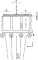
図1及び図2を参照すると、X線源4と、放射線検知器6と、患者支持構造体8と、被写体キャビティ10とを有するガントリ2を含む例示的なCT画像形成システム1が示されており、該X線源4及び該放射線検知器6は、該被写体キャビティ10により分離されるように、対向して配設される。患者12のような被写体を、移動可能な患者支持構造体8(「テーブル」)の上に配設し、その後、該患者支持構造体は、被写体キャビティ10を通る軸線3に沿って移動させられる。X線源4は、X線ビーム14を、患者12を通過させる意図のもとに放射線検知器の方向に照射する。X線ビーム14は、コリメートにより平行光にされ、「画像形成平面」と呼ばれるデカルト座標系のX−Y平面内に位置するようにされる。患者12を通過し、該患者により減衰された後、減衰されたX線ビーム16は、放射線検知器6により受信される。放射線検知器6は、複数の検知器要素18を含み、各々の該検知器要素18が減衰されたX線ビーム16を受信し、該減衰されたX線ビーム16の強さに対応して、電気信号を生成する。
With reference to FIGS. 1 and 2, an exemplary
ガントリ2の1つの角度における放射線検知器からの一群のX線減衰測定値、例えば照射データは、「ビュー(視野)」と呼ばれ、「ビュー」としてここに表示される。被写体の「走査」は、X線源及び放射線検知器6が1回転する間に異なるガントリ角度、すなわちビュー角において形成される一組のビューを含む。軸方向走査においては、照射データは、被写体を通して取られた2次元の「スライス」に対応する画像を構成するために処理され、ここで一つのスライスは、Z方向におけるスライス厚に相当する。
A group of x-ray attenuation measurements from a radiation detector at one angle of the
更に、X線源4及び放射線検知器6は、ガントリ2及び患者支持構造体8に対して回転するように配設され、該患者支持構造体8が被写体キャビティ10内に位置させられたとき、該X線源4及び該放射線検知器6が該患者支持構造体8の周りで回転することを可能にする。X線照射データは、走査の間にX線源4及び放射線検知器6を患者12の周りで回転させることにより得られる。螺旋状X線照射データは、付加的に患者12を軸線3に沿って移動させることにより得られる。X線源4及び放射線検知器6は、CT画像形成システム1と関連する制御機構20と通信する。制御機構20は、X線源4及び放射線検知器6の回転及び作動を制御する。
Furthermore, the X-ray source 4 and the
制御機構20は、X線源4と通信するX線制御装置22と、ガントリモータ制御装置24と、データ取得システム(「DAS」)26とを含む。DAS26は、放射線検知器6と通信する。X線制御装置22は、電力及びタイミング信号をX線源4に与え、ガントリモータ制御装置24は、該X線源4の回転速度及び角度位置を制御し、DAS26は、検知器要素18により生成された電気信号を受信し、該信号を後続する処理のためにデータ信号に変換する。CT画像形成システム1は、画像再構成装置28と、データ格納装置30と、処理装置32とを含み、該処理装置32は、画像再構成装置28と、ガントリモータ制御装置24と、X線制御装置22と、データ格納装置30と、入力装置34と、出力装置36と通信する。データ格納装置30は、当業者に知られている何らかのコンピュータ使用可能格納媒体を備え、伝播されたコンピュータデータ信号5を介して、処理装置32と通信する。CT画像形成システム1は更に、処理装置32及び患者支持構造体8と通信するテーブル制御装置38を含み、該患者支持構造体8の位置を被写体キャビティ10に対して制御するようにする。
The control mechanism 20 includes an
患者12は、患者支持構造体8上に配設されるのが好ましく、その後、被写体キャビティ10内で移動可能であるように、処理装置32を介してオペレータにより位置決めされる。ガントリモータ制御装置24は、処理装置32を介して作動し、X線源4及び放射線検知器6を患者12に対して回転するようにする。X線制御装置22は、処理装置32を介して作動し、X線源4が平行光にされたX線ビーム14を放射線検知器6の方向に、すなわち患者12の方向に放射し、かつ照射するようにする。X線ビーム14は、放射線検知器6により受信される減衰されたX線ビーム16を生成するように、患者12を通過する。
The
検知器要素18は更にセルとも示され、減衰されたX線ビーム16を受信し、該減衰されたX線ビーム16の強さに対応した電気信号を生成し、この電気信号データをDAS26に伝播する。DAS26は、次に、電気信号をデータ信号に変換し、該データ信号を画像再構成装置28に通信する。画像再構成装置は、高速の画像再構成を行なう。再構成された画像がデータ格納装置30に格納され、また出力装置36により表示される。
The
ここで図3ないし図6を参照すると、放射線検知器6の描画が示されている。例示的な実施形態において、放射線検知器6は、多次元の検知器要素18の検知器アレイとして構成される。放射線検知器6のアレイを、長さγ(ガンマ)のアーク長のセグメント及び軸線3に沿った線形の(この場合において)深さnとして、構成することができる。この長さは、以下において、放射線検知器6についてのチャネルγとして知られ、βはビューを表し、nは本明細書で前に述べたように行を表す。
Referring now to FIGS. 3-6, a drawing of the
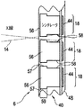
各々の検知器要素18は、シンチレータ46と光センサ44とを含む。光センサ44を、基板48上に蒸着させるか又は基板48上に形成することができ、シンチレータアレイ46は、基板48の上方に位置させられ、かつ該基板に固定される。光センサ44は、光学的にシンチレータ46に結合され、該シンチレータ46により出力された光を表す信号を送信するための電気出力ラインを含む。具体的には、各々の光センサ44は、特定のシンチレータ46についてのビーム減衰の測定値である別々の低水準の電気的アナログ出力信号を生成する。
Each
放射線検知器6の例示的な構成は、検知器要素18の約24の行nとγ(ガンマ)で示される約912の列の「検知器チャネル」とを含む。放射線検知器6についてのそのようなアレイ構成は、ガントリ2(図1に示す)の各回転で収集される約16個までのデータの同時スライスを画像形成することを可能にする。更に、放射線検知器6を、多くの異なるスライス厚及び数のモードで作動させることができる。イネーブルすることができ、ディスエーブルすることができ、或いは組み合わせることができる光センサ44の出力の特定の種々の組み合わせにより、スライス厚を、例えば、約0.625mm、1.25mm、2.5mm、3.75mm、又は5mmとすることができる。付加的な例は、約0.625mm厚から約20mm厚までの範囲のスライスの1つを含む単一スライスモードと、約0.625mm厚から10mm厚までの範囲のスライスの2つを含む2スライスモードとを含む。もちろん、多くの他のモードが可能である。
An exemplary configuration of the
放射線検知器6を、シンチレータ46及び光センサ44を含む検知器要素18のアレイに関して説明するが、他の構成も達成可能であり利用されることを理解されたい。例えば、放射線検知器6を、多次元アレイの組み合わせとして構成することができ、1つの場合において、多次元シンチレータアレイと高密度半導体(光センサ)アレイとの組み合わせとして構成することができる。シンチレータアレイは、アレイ状に並べられた複数のシンチレーション素子を含むことができ、半導体アレイは、複数の光センサ、例えば、同一アレイ状に並べられた光ダイオードを含む。光センサは、基板上に蒸着され又は形成され、シンチレータアレイは、基板の上方に位置させられ、かつ該基板に固定される。
Although the
画像形成アレイは、これに限られるものではないが、シンチレーション用媒体に結合された光センサを含む。シンチレータに吸収される放射線は光学的フォトンを発生し、次に、これに限られるものではないが、光トランジスタ又は光ダイオードを含むが光センサに送られる。フォトンは光センサに吸収され、入射したフォトンフラックスに対応する電気信号が発生させられる。光センサ又は光ダイオードのような如何なる感光性の素子も、薄膜トランジスタ(TFT)のような必要な制御又はスイッチング素子と関連させて比較的大きなアレイに形成することができる。放射線検知器6は、典型的には、大きな基板上に形成され、該基板上に、TFT、アドレスライン、コンデンサ及び光センサのような装置を含む多数の構成要素が、導電材料、半導体材料及び絶縁材料の層の蒸着及びパターン形成により形成される。
The imaging array includes, but is not limited to, a light sensor coupled to a scintillation medium. The radiation absorbed by the scintillator generates optical photons, which are then sent to an optical sensor, including but not limited to a phototransistor or photodiode. The photons are absorbed by the optical sensor, and an electrical signal corresponding to the incident photon flux is generated. Any photosensitive elements such as photosensors or photodiodes can be formed in a relatively large array in conjunction with the necessary control or switching elements such as thin film transistors (TFTs). The
図4は、シンチレータ46については通常の構成を用いる放射線検知器6の一部を示すものであり、各々の検知器要素18は、X線ビームの焦点スポットの位置に対する該要素のX軸及びZ軸方向位置に応じた角度の範囲(1つの次元しか図示されていない)からX線を受ける。ワイヤをZ軸に置き、プレートをX軸に置くことにより、Z軸におけるセルの縁部がX線から遮蔽され、従って、出力信号に影響しなくなる。例えば、CT検知器についての角度の範囲は、該検知器の末端の縁部においておおよそ±1度である。この場合において、セルが無線構成においてX線により励起されている場合は、該セルがX線平面から遠ければ遠いほど傾斜角が大きくなり、縁部からの信号における影響が高くなる。シンチレーション・セグメント(Z軸方向においてはスライスとも呼ばれる)は、タングステンワイヤにより遮蔽された非シンチレーション・リフレクタ(低Z値)により分離される。シンチレーション光(X線が光に変換されることにより発生されられた)は、次に、複数回の反射により光センサ44の方向に向けられる。特に、実効幾何学的効率(実効露光面積)はセルに対する垂直からの角度とともに増加するので、セル縁部がX線に当たることによる縁部の露光と光の生成とが原因となって、シンチレーション応答は、X線がセルに対して垂直であるときに最小になり、垂直からの角度の増加とともに増加する。ある光が縁部上で発生されられた場合(X線に露光されたとき)には、この光は、光センサ44に近く、反射及び減衰が少なくなるため、より効率的に収集されることになる。ビーム14がセルの表面入り口に対して垂直でなくなればなくなるほど、シンチレータ46の縁部を励起する機会が高まり、光出力がより高くなる。X線ビーム14がセル検知器要素18の表面に垂直で、その縁部を露光していないときに、最小の利得が生じる。図5は、光センサ44の応答の実験的かつシミュレートされた挙動を、シンチレータ46上へのX線入射角の関数として示す。縁部がスライス内の隣接するセルにおいて異なる場合、対応するセルは、非線形の示差誤差を、焦点スポットの運動の関数として示す。
FIG. 4 shows a portion of a
図4を続けて参照し、特定のスライスを考察すると、該スライス内の各々のセルすなわち検知器要素18は、X線ビーム14に対して僅かに異なる縁部角(又はX軸まわりの回転角)を示し、従って、個々のチャネル(X方向における)又は行すなわちスライス(Z方向における)は、X線ビーム14の運動に対して異なる応答をすることになる。従って、種々の検知器要素18すなわちセルは、特定の利得ポイント、例えば最小利得ポイントについて、僅かな位相差を示す。その結果、X線ビーム14の焦点スポットがZ軸方向(又は別の場合についてはX軸方向)に移動するとき、種々のチャネルの応答は異なるものとなる。図5は、シンチレータ46のシミュレートされた応答をX軸まわりの回転(Z軸における同等の変位)の関数として示す。同様の現象がZ軸まわりの回転について、シンチレータにより示されることに注目されたい。較正目的のためには各々の検知器要素が所定の入力について実質的に同じ応答を示すことが好ましいので、これは望ましくない特性である。
Continuing to refer to FIG. 4, considering a particular slice, each cell or
中央スライスにおける検知器要素が、Z軸におけるビームの運動(焦点スポット)に対しては、他の場所より高い感度を示すことが更に理解されるであろう。図6に、焦点スポットの運動についての例示的な応答を回転角(X軸まわりの)の関数として示す。このグラフの観察は、放射線検知器6の中心で取ったスライスが、傾斜又は回転(この例ではX軸まわりの)の場合の半分に近い感度になるということを示しており、これは中心面からの高さに起因する角度によるものである。焦点スポットの運動は、熱膨張及び重力と相互作用する遠心力のような原因によるものであり、約1mmの範囲を含む。更に、チャネル(及び/又は種々のスライス)間の傾斜の差は、焦点スポットの位置の範囲(±1度)にわたり、約±2%又はそれ以上の示差利得(differential gain)の変化をもたらす。この角度は、検知器要素18と検知器要素18との間(X軸についてのチャネル間としても知られている)の差により定められる。従って、Z軸方向の運動の誤差を以下のように定めることができ、
It will be further appreciated that the detector elements in the central slice are more sensitive to beam motion (focal spot) in the Z axis than elsewhere. FIG. 6 shows an exemplary response for focal spot motion as a function of rotation angle (around the X axis). Observation of this graph shows that the slice taken at the center of the

ここで、
Ch(i)はi番目のチャネルに関連する検知器要素からの出力であり、
Ch(i+1)は(i+1)番目のチャネルに関連する検知器要素からの出力であり、位置は、検知器平面に対するZ軸方向の焦点スポットの場所に対応する。
here,
Ch (i) is the output from the detector element associated with the i th channel,
Ch (i + 1) is the output from the detector element associated with the (i + 1) th channel, and the position corresponds to the location of the focal spot in the Z-axis direction relative to the detector plane.
上の説明及び例はZ軸方向の運動に対してのものであるが、同様の考察がX軸方向の運動に対して適用可能であることを理解されたい。 Although the above description and examples are for Z-axis motion, it should be understood that similar considerations are applicable for X-axis motion.
第3世代CTスキャナは、チャネルとチャネルの間の差について、示差利得誤差(differential gain error)が中央領域においておおよそ0.02%を超えているとき、リング、バンド、及び中心スポットというアーチファクトを生じることがある。補償のために、画像再構成の間、少なくとも幾らかの示差利得値を較正し修正することができる。しかしながら、入射角の変化は変動するものであり、それを追跡することは困難である。それに加えて、異なる組み込み角に起因する変化(すなわち、Z軸方向(及びX軸方向)のセルの位置による角度と、縁部の不完全さによる組み込み傾斜角との組み合わせ)が、無線検知器においてZ軸方向又はX軸方向に焦点スポットが移動するとき、利得の非線形変化を誘起することになる。この非線形の挙動は補償することが困難で、付加的な手順、並びに、1つ1つのセルにおける長い較正時間を必要とする。更に、スキャナ作動中の焦点スポットの運動に起因する示差利得は、ソフトウェアのアルゴリズムを用いる場合でも容易には修正できない。 Third generation CT scanners produce ring, band, and center spot artifacts for the difference between channels when the differential gain error exceeds approximately 0.02% in the central region. Sometimes. For compensation, at least some differential gain values can be calibrated and corrected during image reconstruction. However, the change of the incident angle is fluctuating and it is difficult to track it. In addition, changes due to different built-in angles (ie, the combination of the angle due to the cell position in the Z-axis direction (and the X-axis direction) and the built-in tilt angle due to edge imperfections) are detected by the wireless detector. When the focal spot moves in the Z-axis direction or the X-axis direction, a non-linear change in gain is induced. This non-linear behavior is difficult to compensate and requires additional procedures as well as long calibration times in each cell. In addition, the differential gain due to focal spot motion during scanner operation cannot be easily corrected using software algorithms.
本発明の実施形態は、シンチレータの縁部上及び光センサに衝突するX線について、同じスライスのチャネル間の差が、X線ビーム角又はZ軸方向(又は別の場合においてはX軸方向)の焦点スポットの運動に影響を受けなくなるような方法を提供する。例示的な実施形態において、このことは、X線ビーム14がシンチレータ、例えばシンチレータ56及び66の縁部と接触しないように、又は、少なくとも、焦点スポットの検知器と該スポットの運動範囲との間の距離により定められる角度の範囲においての該シンチレータ56及び66の特定の傾斜について、接触が少なくなるように、検知器要素18すなわちセルを構成することにより達成される。更に、改良されたシンチレータ、例えばシンチレータ56及び66が、前に説明した遮蔽用ワイヤを除くことの助けとなり、従って、放射線検知器6を製作するための費用が削減される。ここに開示した実施形態の別の利点は、従来の構成における遮蔽用ワイヤを除くことによりもたらされる較正時間すなわち試験時間の削減である。更に、ここに開示した実施形態は、X線ビーム14の運動(X軸方向又はZ軸方向)に対して低減された感度を示すため、運動により誘起されるアーチファクトが減少する。運動に基づくアーチファクトの減少は、画像の明確さを高め、検知を改善する。最後に、現在の放射線検知器における遮蔽用ワイヤの除去により、照射効率が改良され、患者に対する影響が最小になる。
Embodiments of the present invention show that for X-rays impinging on the scintillator edge and on the optical sensor, the difference between channels in the same slice is the X-ray beam angle or Z-axis direction (or X-axis direction in other cases) Provide a way to be insensitive to the movement of the focal spot. In the exemplary embodiment, this is done so that the
図7及び図8は、各々、検知器要素18が、改善された幾何学的形状のシンチレータ56及び66のそれぞれを含む例示的な放射線検知器6の一部を示す。図は、シンチレータ56及び66それぞれの幾何学的形状の断面図を、1つの軸において(例えば、Z軸又はX軸に沿って)示す。例示的な実施形態において、シンチレータ56は、ほぼ立方体形状であり、焦点スポット位置の運動範囲にわたり、シンチレータ55及び66のそれぞれの縁部/側部に、X線が全く当たらないか又は非常に小さいX線成分しか当たらないように構成され、それによって、前に説明したX線ビーム14の変化に対してほぼ均一な応答を生み出すようになる。例えば、図7を参照すると、シンチレータ56の側部が、拡大された部分、フランジ、又は張り出し部分57を含んでおり、該張り出し部分57は、選択された運動の量のもとで入射X線ビーム14が、光センサ44に対して最も近いシンチレータ56の縁部58の一部に当たるのを防ぐものである。拡大された部分すなわち張り出し部分57の厚さ、並びに、該張り出し部分の深さ59を、必要に応じて、所望の遮蔽効果をもたらす幾何学的形状になるように選択することができる。例えば、X線ビーム14の所定の変化について、拡大された部分すなわち張り出し部分57を、深さ59が大きいが、薄い形状にした場合には、拡大された部分すなわち張り出し部分57を大きくし、深さ59を小さくしたものがもたらすのと同様の遮蔽をもたらす。正確な構成は、必要に応じて、遮蔽を満足させるように、並びに、寸法(セルの大きさ、焦点スポットと検知器との距離、スライスにおけるセルの場所、焦点スポットの運動範囲等)に基づく製造上の制約を満足させるように選択することができる。シンチレータは、階段状のカットを用いて、放射線ビーム14を受ける第2表面から光センサ44に対して近位にある第1表面まで外向きに先細にされて、選択された焦点スポットの運動の範囲に対しては、放射線ビーム14が、光センサ44の付近において、別の側部68上に衝突しないようになっている。
FIGS. 7 and 8 each show a portion of an
同様に、別の実施形態における図8を参照すると、この場合にも、選択された焦点スポットの運動の量において、入射X線ビーム14がシンチレータ66の側部68上に当たるのを妨げるように、シンチレータ66の側部68がカットされ、光センサ44から外側に向う方向に先細にされていることが分かる。ここでも、先細部分を、必要に応じて、遮蔽の必要条件を満たすように、並びに、寸法(セルの大きさ、焦点スポットと検知器との距離、スライスにおけるセルの場所、焦点スポットの運動範囲等)に基づく製造上の制約を満足させるように選択することができることが明らかであろう。
Similarly, referring to FIG. 8 in another embodiment, again, to prevent the
上述した各々の例において、シンチレータ、例えばシンチレータ56及び66に対する改善が、単一の軸(例えばZ軸)に関して述べられていることに注目されたい。もちろん、同様の適用例を、他の軸(例えばX軸)のために適用することができる。
Note that in each example described above, improvements to the scintillators, eg,
前の実施形態は医療用の画像形成に関して説明されているが、ここに述べた画像の取得及び処理方法は医療用用途に限定されるものではなく、医療用ではない用途に利用することができることが理解されるであろう。 Although the previous embodiment has been described with respect to medical image formation, the image acquisition and processing methods described here are not limited to medical applications, and can be used for non-medical applications. Will be understood.
本明細書で用いられる、単数で記載され、「数詞」が前に置かれていない要素又は段階は、その除外が明示的に記載されていない限り、複数の要素又は段階を除外するものではないと理解されたい。更に、本発明の「実施形態」又は「1つの」「実施形態」を参照することは、更に挙げられる特徴を組み入れる付加的な実施形態の存在を除外するものとして解釈することを意図するものではない。更に、ここで用いられる、「画像を再構成する」という語句は、画像を表すデータは生成されるが可視画像がないような本発明の実施形態を排除することを意図するものではない。しかしながら、多くの実施形態では、少なくとも1つの可視画像が生成される(又は生成されるように構成されている)。 As used herein, an element or step described in the singular and not preceded by a “numerical number” does not exclude a plurality of elements or steps unless the exclusion is explicitly stated. Please understand. Furthermore, references to “embodiments” or “one” “embodiments” of the present invention are not intended to be interpreted as excluding the existence of additional embodiments that also incorporate the recited features. Absent. Furthermore, as used herein, the phrase “reconstruct an image” is not intended to exclude embodiments of the invention in which data representing the image is generated but there is no visible image. However, in many embodiments, at least one visible image is generated (or configured to be generated).
上の実施形態を用いた説明は、例示的なものに過ぎない。上述のように、これらのプロセスを実施するためのコンピュータ実行プロセス及び装置の形態である実施形態を含むことができる。更に、フレキシブルディスク、CD−ROM、ハードドライブ又は他のコンピュータ可読格納媒体のような有形の媒体内に具現された指示を含むコンピュータプログラムコードの形態である実施形態を含むことができ、該コンピュータプログラムコードがコンピュータ中にロードされ、該コンピュータにより実行されたとき、該コンピュータは、本発明を実行するための装置となる。更に、例えば、格納媒体に格納されるか、コンピュータ中にロードされ及び/又はコンピュータにより実行されるか、又は送信されたデータ信号として伝播されたコンピュータプログラムコードの形態であるか、光ファイバを通る又は電磁放射線を介する電気配線又はケーブル配線にわたるような幾つかの送信媒体にわたる変調された搬送波であるか又は搬送波ではないコンピュータプログラムコードの形態である実施形態を含むことができ、該コンピュータプログラムコードがコンピュータ中にロードされ、該コンピュータにより実行されたとき、該コンピュータは、本発明を実行するための装置となる。汎用マイクロプロセッサ上に実装されるとき、コンピュータプログラムコードのセグメントは、該マイクロプロセッサを構成して、特定の論理回路を生成する。 The description using the above embodiment is merely exemplary. As described above, embodiments can be included that are in the form of computer-implemented processes and apparatus for performing these processes. Furthermore, the present invention can include embodiments in the form of computer program code including instructions embodied in a tangible medium such as a flexible disk, CD-ROM, hard drive or other computer readable storage medium. When code is loaded into and executed by a computer, the computer becomes an apparatus for carrying out the present invention. Further, for example, in the form of computer program code stored in a storage medium, loaded into a computer and / or executed by a computer, or propagated as a transmitted data signal, or through an optical fiber. Or an embodiment that is in the form of a modulated or non-carrier computer program code over several transmission media, such as over electrical wiring or cabling via electromagnetic radiation, the computer program code being When loaded into a computer and executed by the computer, the computer becomes an apparatus for carrying out the present invention. When implemented on a general-purpose microprocessor, the computer program code segments configure the microprocessor to create specific logic circuits.
本発明を例示的な実施形態に関して説明してきたが、本発明の技術的範囲から離れることなく、種々の変更を行なうことができ、また均等技術をその実施形態の要素と置き換えることができることは、当業者には明らかであろう。更に、本発明の本質的な技術的範囲から離れることなく、本発明の教示に対して特定の状況又は材料を適合させるように、多数の修正を行なうことができる。従って、本発明は、本発明を実行するために開示した特定の実施形態に限定されるものではなく、本発明は、同時に提出した特許請求の範囲の技術的範囲内にあるすべての実施形態を含むことを意図している。 Although the present invention has been described in terms of exemplary embodiments, it will be understood that various changes can be made without departing from the scope of the invention, and that equivalent techniques can be substituted for elements of the embodiments. It will be apparent to those skilled in the art. In addition, many modifications may be made to adapt a particular situation or material to the teachings of the invention without departing from the essential scope of the invention. Accordingly, the invention is not limited to the specific embodiments disclosed for carrying out the invention, but the invention encompasses all embodiments within the scope of the appended claims. Intended to include.
6 放射線検知器
14 放射線ビーム
18 放射線検知器要素
44 光センサ
46、56、66 シンチレータ
48 基板
57 フランジ
58 縁部
68 側部
6
Claims (10)
放射線検知器要素(18)組立体であって、
シンチレータ(46)(56)(66)と光センサ(44)とを備え、
前記シンチレータが、前記光センサ(44)に対して近位にある第1表面と、前記第1表面に対して遠位にあり放射線ビーム(14)を受ける第2表面とを含む放射線検知器要素(18)組立体とを含み、
前記シンチレータ(46)(56)(66)の側部(68)が、その上への放射線ビーム(14)の衝突を遮って、該側部(68)への前記衝突に対する前記光センサ(44)の応答を減らすように構成され、
前記シンチレータ(46)(56)(66)が、前記第2表面から前記第1表面まで外向きに先細にされて、選択された焦点スポットの運動の範囲に対しては、前記放射線ビーム(14)が、前記光センサ(44)の付近において、隣のシンチレータの側部(68)上に衝突しないようになっており、
前記第1表面における前記シンチレータ(46)(56)(66)の大きさが、焦点スポットの運動の範囲により定められることを特徴とする画像形成システム。 A radiation source;
A radiation detector element (18) assembly comprising:
A scintillator (46) (56) (66) and an optical sensor (44);
A radiation detector element wherein the scintillator includes a first surface proximal to the photosensor (44) and a second surface distal to the first surface and receiving a radiation beam (14). (18) including an assembly,
The side (68) of the scintillator (46) (56) (66) blocks the collision of the radiation beam (14) thereon, and the optical sensor (44) against the collision on the side (68). ) To reduce response,
The scintillator (46) (56) (66), are tapered outwardly from the second surface to the first surface, with respect to the range of motion of the focal spot is selected, the radiation beam (14 ) Does not collide with the side (68) of the adjacent scintillator in the vicinity of the photosensor (44),
The size of the scintillators (46) (56) (66) on the first surface is determined by the range of motion of the focal spot.
画像形成システムにおいて用いられる放射線検知器アレイ(6)であって、
複数の光センサ(44)を含む光センサ(44)アレイと作動可能な構成で配設された、複数のシンチレータ(46)(56)(66)を含むシンチレータ(46)(56)(66)アレイを備える放射線検知器アレイ(6)とを含み、
前記複数のシンチレータ(46)(56)(66)の各々のシンチレータ(46)(56)(66)が、前記複数の光センサ(44)の光センサ(44)に対して近位にある第1表面と、前記第1表面に対して遠位にあり放射線ビーム(14)を受ける第2表面とを含み、
前記各々のシンチレータ(46)(56)(66)の側部(68)が、その上に衝突する放射線ビームを遮って、該側部への前記衝突に対する各々の光センサ(44)のそれぞれの応答を減らすように構成され、
前記シンチレータ(46)(56)(66)が、前記第2表面から前記第1表面まで外向きに先細にされて、選択された焦点スポットの運動の範囲に対しては、前記放射線ビーム(14)が、前記光センサ(44)の付近において、隣のシンチレータの側部(68)上に衝突しないようになっており、
前記第1表面における前記シンチレータ(46)(56)(66)の大きさが、焦点スポットの運動の範囲により定められることを特徴とする画像形成システム。 A radiation source;
A radiation detector array (6) for use in an imaging system comprising:
A scintillator (46) (56) (66) including a plurality of scintillators (46) (56) (66) disposed in an operable configuration with an array of photosensors (44) including a plurality of photosensors (44). A radiation detector array (6) comprising an array,
A scintillator (46) (56) (66) of each of the plurality of scintillators (46) (56) (66) is proximal to a light sensor (44) of the plurality of light sensors (44). A first surface and a second surface distal to the first surface and receiving a radiation beam (14);
The side (68) of each of the scintillators (46) (56) (66) blocks the radiation beam impinging thereon and the respective optical sensor (44) for each of the collisions to the side Configured to reduce response,
The scintillator (46) (56) (66), are tapered outwardly from the second surface to the first surface, with respect to the range of motion of the focal spot is selected, the radiation beam (14 ) Does not collide with the side (68) of the adjacent scintillator in the vicinity of the photosensor (44),
The size of the scintillators (46) (56) (66) on the first surface is determined by the range of motion of the focal spot.
前記第2表面が、前記放射線ビーム(14)の一部が衝突し、前記衝突に対する前記光センサ(44)の応答を減らすように、前記第1表面より大きく構成されることを特徴とする、請求項1又は2に記載の画像形成システム。 The scintillator (46) (56) the side of (66) (68) has a stepped cut,
The second surface is configured to be larger than the first surface so that a portion of the radiation beam (14) impinges and reduces the response of the photosensor (44) to the collision; The image forming system according to claim 1.
前記シンチレータ(46)(56)(66)と前記光センサ(44)が、X−Z平面に沿って配列されており、
前記放射線ビーム(14)がY軸の方向に沿って照射され、
前記側部(68)がX軸と平行であることを特徴とする、請求項1に記載の画像形成システム。 A patient support structure (8) movable in the Z-axis direction;
The scintillators (46) (56) (66) and the photosensor (44) are arranged along the XZ plane,
The radiation beam (14) is irradiated along the direction of the Y axis;
The image forming system according to claim 1, wherein the side portion is parallel to the X axis.
放射線源を用意する段階と、
放射線検知器要素(18)組立体を用意する段階と、
前記放射線源と、前記放射線検知器要素(18)組立体と、被写体キャビティ(10)とを有し、前記放射線源と、前記放射線検知器要素(18)組立体とを回転させるガントリ(2)を用意する段階とを含み、
前記ガントリに含まれる前記放射線検知器要素(18)組立体が、
遮蔽用ワイヤを備えず、
シンチレータ(46)(56)(66)と光センサ(44)とを備え、
前記シンチレータが、前記光センサ(44)に対して近位にある第1表面と、前記第1表面に対して遠位にあり放射線ビーム(14)を受ける第2表面とを含む放射線検知器要素(18)組立体とを含み、
前記シンチレータ(46)(56)(66)の側部(68)が、その上への放射線ビーム(14)の衝突を遮って、該側部(68)への前記衝突に対する前記光センサ(44)の応答を減らすように構成され、
前記シンチレータ(46)(56)(66)が、前記第2表面から前記第1表面まで外向きに先細にされて、選択された焦点スポットの運動の範囲に対しては、前記放射線ビーム(14)が、前記光センサ(44)の付近において、隣のシンチレータの側部(68)上に衝突しないようになっており、
前記第1表面における前記シンチレータ(46)(56)(66)の大きさが、焦点スポットの運動の範囲により定められることを特徴とする方法。 A method for manufacturing an image forming system, comprising:
Providing a radiation source;
Providing a radiation detector element (18) assembly;
A gantry (2) having the radiation source, the radiation detector element (18) assembly, and a subject cavity (10) for rotating the radiation source and the radiation detector element (18) assembly. Preparing a stage,
The radiation detector element (18) assembly included in the gantry includes:
Without shielding wire,
A scintillator (46) (56) (66) and an optical sensor (44);
A radiation detector element wherein the scintillator includes a first surface proximal to the photosensor (44) and a second surface distal to the first surface and receiving a radiation beam (14). (18) including an assembly,
The side (68) of the scintillator (46) (56) (66) blocks the collision of the radiation beam (14) thereon, and the optical sensor (44) against the collision on the side (68). ) To reduce response,
The scintillator (46) (56) (66), are tapered outwardly from the second surface to the first surface, with respect to the range of motion of the focal spot is selected, the radiation beam (14 ) Does not collide with the side (68) of the adjacent scintillator in the vicinity of the photosensor (44),
A method wherein the size of the scintillators (46) (56) (66) on the first surface is determined by the range of motion of the focal spot.
光センサ(44)に対して近位にある第1表面と、前記第1表面に対して遠位にある第2表面とを含むシンチレータ(46)(56)(66)の前記第2表面上に入射する放射線ビーム(14)を受け、
前記シンチレータ(46)(56)(66)の側部(68)上への衝突に対する前記光センサ(44)の応答を減らすように構成された該側部(68)により放射線ビーム(14)の衝突を遮る、
段階を含み、
前記シンチレータ(46)(56)(66)が、前記第2表面から前記第1表面まで外向きに先細にされて、選択された焦点スポットの運動の範囲に対しては、前記放射線ビーム(14)が、前記光センサ(44)の付近において、隣のシンチレータの側部(68)上に衝突しないようになっており、
前記第1表面における前記シンチレータ(46)(56)(66)の大きさが、焦点スポットの運動の範囲により定められることを特徴とする方法。 A method for detecting an incident radiation beam (14), comprising:
On the second surface of the scintillators (46) (56) (66) comprising a first surface proximal to the optical sensor (44) and a second surface distal to the first surface Receiving a radiation beam (14) incident on
Of the radiation beam (14) by the side (68) configured to reduce the response of the photosensor (44) to impact on the side (68) of the scintillator (46) (56) (66). Block the collision,
Including stages,
The scintillator (46) (56) (66), are tapered outwardly from the second surface to the first surface, with respect to the range of motion of the focal spot is selected, the radiation beam (14 ) Does not collide with the side (68) of the adjacent scintillator in the vicinity of the photosensor (44),
A method wherein the size of the scintillators (46) (56) (66) on the first surface is determined by the range of motion of the focal spot.
前記第2表面を前記第1表面より大きく構成し、前記放射線ビーム(14)の一部が前記第2表面上だけに衝突し、前記衝突に対する前記光センサ(44)の応答を減らすようにすることを特徴とする、請求項7又は8に記載の方法。 The scintillator (46) (56) the side of (66) (68) has a stepped cut,
The second surface is configured to be larger than the first surface so that a portion of the radiation beam (14) impinges only on the second surface and reduces the response of the photosensor (44) to the collision. The method according to claim 7 or 8, characterized in that:
Applications Claiming Priority (1)
| Application Number | Priority Date | Filing Date | Title |
|---|---|---|---|
| US10/064,590 US6979826B2 (en) | 2002-07-29 | 2002-07-29 | Scintillator geometry for enhanced radiation detection and reduced error sensitivity |
Publications (3)
| Publication Number | Publication Date |
|---|---|
| JP2004061516A JP2004061516A (en) | 2004-02-26 |
| JP2004061516A5 JP2004061516A5 (en) | 2008-09-11 |
| JP4518759B2 true JP4518759B2 (en) | 2010-08-04 |
Family
ID=30113652
Family Applications (1)
| Application Number | Title | Priority Date | Filing Date |
|---|---|---|---|
| JP2003280542A Expired - Fee Related JP4518759B2 (en) | 2002-07-29 | 2003-07-28 | Image forming system, method of manufacturing image forming system, and method of detecting incident radiation beam |
Country Status (3)
| Country | Link |
|---|---|
| US (1) | US6979826B2 (en) |
| EP (1) | EP1387185A1 (en) |
| JP (1) | JP4518759B2 (en) |
Families Citing this family (25)
| Publication number | Priority date | Publication date | Assignee | Title |
|---|---|---|---|---|
| RU2007125632A (en) * | 2004-12-09 | 2009-01-20 | Конинклейке Филипс Электроникс Н.В. (Nl) | CELLULAR DETECTORS SENSITIVE TO THE DEPTH OF INTERACTION |
| US20070086565A1 (en) * | 2005-10-13 | 2007-04-19 | Thompson Richard A | Focally aligned CT detector |
| US7521685B2 (en) * | 2006-01-18 | 2009-04-21 | General Electric Company | Structured scintillator and systems employing structured scintillators |
| US7676073B2 (en) * | 2006-08-29 | 2010-03-09 | Siemens Medical Solutions Usa, Inc. | System and method for reducing circular artifacts in tomographic imaging |
| US20090213984A1 (en) * | 2008-02-26 | 2009-08-27 | United Technologies Corp. | Computed Tomography Systems and Related Methods Involving Post-Target Collimation |
| US7639777B2 (en) * | 2008-02-26 | 2009-12-29 | United Technologies Corp. | Computed tomography systems and related methods involving forward collimation |
| US8238521B2 (en) * | 2008-03-06 | 2012-08-07 | United Technologies Corp. | X-ray collimators, and related systems and methods involving such collimators |
| US20090225954A1 (en) * | 2008-03-06 | 2009-09-10 | United Technologies Corp. | X-Ray Collimators, and Related Systems and Methods Involving Such Collimators |
| US7876875B2 (en) * | 2008-04-09 | 2011-01-25 | United Technologies Corp. | Computed tomography systems and related methods involving multi-target inspection |
| US7888647B2 (en) * | 2008-04-30 | 2011-02-15 | United Technologies Corp. | X-ray detector assemblies and related computed tomography systems |
| US20090274264A1 (en) * | 2008-04-30 | 2009-11-05 | United Technologies Corp. | Computed Tomography Systems and Related Methods Involving Localized Bias |
| US8941070B2 (en) * | 2008-11-19 | 2015-01-27 | General Electric Company | Portable digital image detector positioning apparatus |
| JP5400546B2 (en) * | 2009-09-28 | 2014-01-29 | 株式会社日立メディコ | X-ray CT system |
| US8258479B2 (en) * | 2009-12-15 | 2012-09-04 | Saint-Gobain Ceramics & Plastics, Inc. | Radiation detection system and method of making a radiation detection system |
| US20110211667A1 (en) * | 2010-02-26 | 2011-09-01 | Abdelaziz Ikhlef | De-populated detector for computed tomography and method of making same |
| US8155265B2 (en) | 2010-07-15 | 2012-04-10 | General Electric Company | Asymmetric de-populated detector for computed tomography and method of making same |
| US8204171B2 (en) | 2010-10-11 | 2012-06-19 | General Electric Company | Multi-faceted tileable detector for volumetric computed tomography imaging |
| US8548119B2 (en) | 2011-01-13 | 2013-10-01 | General Electric Company | Multi-slice CT detector with tileable packaging structure |
| US9168008B2 (en) | 2011-11-03 | 2015-10-27 | General Electric Company | Coarse segmented detector architecture and method of making same |
| US9689996B2 (en) * | 2013-04-05 | 2017-06-27 | General Electric Company | Integrated diode DAS detector |
| JP2015025665A (en) | 2013-07-24 | 2015-02-05 | ソニー株式会社 | Radiation imaging apparatus and radiation imaging display system |
| US11156727B2 (en) * | 2015-10-02 | 2021-10-26 | Varian Medical Systems, Inc. | High DQE imaging device |
| EP4080249A1 (en) | 2016-04-15 | 2022-10-26 | Saint-Gobain Ceramics and Plastics, Inc. | Photosensors arranged on a surface of a scintillator |
| JP6740943B2 (en) * | 2017-03-28 | 2020-08-19 | コニカミノルタ株式会社 | Radiation conversion panel and Talbot imager |
| US11944476B2 (en) | 2021-04-22 | 2024-04-02 | MinFound Medical Systems Co., Ltd. | Apparatus and method of assembly of module for a CT detector |
Citations (6)
| Publication number | Priority date | Publication date | Assignee | Title |
|---|---|---|---|---|
| JPH0511060A (en) * | 1990-01-29 | 1993-01-19 | General Electric Co <Ge> | Two-dimensional mosaic scintillation detector |
| JPH0836059A (en) * | 1994-07-25 | 1996-02-06 | Shimadzu Corp | Radiation detector |
| JPH0886879A (en) * | 1994-09-19 | 1996-04-02 | Hamamatsu Photonics Kk | Scintillation detector |
| JPH09325185A (en) * | 1996-06-03 | 1997-12-16 | Toshiba Fa Syst Eng Kk | Radiation detector, its manufacture, fluorographic apparatus and ct scanner |
| US20020067796A1 (en) * | 2000-12-05 | 2002-06-06 | Hoffman David M. | System and method of computed tomography imaging using a focused scintillator and method of manufacturing same |
| JP2002181940A (en) * | 2000-12-15 | 2002-06-26 | Canon Inc | Wavelength conversion-type light sensor |
Family Cites Families (10)
| Publication number | Priority date | Publication date | Assignee | Title |
|---|---|---|---|---|
| US4234792A (en) * | 1977-09-29 | 1980-11-18 | Raytheon Company | Scintillator crystal radiation detector |
| US4180737A (en) * | 1978-02-06 | 1979-12-25 | General Electric Company | X-ray detector |
| US4159424A (en) * | 1978-04-03 | 1979-06-26 | General Electric Company | Trapezoidal scintillator for radiation detectors |
| US4323925A (en) * | 1980-07-07 | 1982-04-06 | Avco Everett Research Laboratory, Inc. | Method and apparatus for arraying image sensor modules |
| US5059800A (en) * | 1991-04-19 | 1991-10-22 | General Electric Company | Two dimensional mosaic scintillation detector |
| US5241180A (en) * | 1992-08-05 | 1993-08-31 | General Electric Company | Radiation detection devices with tapered scintillator crystals |
| CA2194942A1 (en) | 1996-01-18 | 1997-07-19 | William P. Novak | Radiation detector with improved response |
| US6344649B2 (en) * | 1997-11-26 | 2002-02-05 | General Electric Company | Scintillator for a multi-slice computed tomograph system |
| US6295331B1 (en) * | 1999-07-12 | 2001-09-25 | General Electric Company | Methods and apparatus for noise compensation in imaging systems |
| US6414315B1 (en) * | 1999-10-04 | 2002-07-02 | General Electric Company | Radiation imaging with continuous polymer layer for scintillator |
-
2002
- 2002-07-29 US US10/064,590 patent/US6979826B2/en not_active Expired - Fee Related
-
2003
- 2003-07-18 EP EP03254499A patent/EP1387185A1/en not_active Withdrawn
- 2003-07-28 JP JP2003280542A patent/JP4518759B2/en not_active Expired - Fee Related
Patent Citations (6)
| Publication number | Priority date | Publication date | Assignee | Title |
|---|---|---|---|---|
| JPH0511060A (en) * | 1990-01-29 | 1993-01-19 | General Electric Co <Ge> | Two-dimensional mosaic scintillation detector |
| JPH0836059A (en) * | 1994-07-25 | 1996-02-06 | Shimadzu Corp | Radiation detector |
| JPH0886879A (en) * | 1994-09-19 | 1996-04-02 | Hamamatsu Photonics Kk | Scintillation detector |
| JPH09325185A (en) * | 1996-06-03 | 1997-12-16 | Toshiba Fa Syst Eng Kk | Radiation detector, its manufacture, fluorographic apparatus and ct scanner |
| US20020067796A1 (en) * | 2000-12-05 | 2002-06-06 | Hoffman David M. | System and method of computed tomography imaging using a focused scintillator and method of manufacturing same |
| JP2002181940A (en) * | 2000-12-15 | 2002-06-26 | Canon Inc | Wavelength conversion-type light sensor |
Also Published As
| Publication number | Publication date |
|---|---|
| US6979826B2 (en) | 2005-12-27 |
| EP1387185A1 (en) | 2004-02-04 |
| JP2004061516A (en) | 2004-02-26 |
| US20040016885A1 (en) | 2004-01-29 |
Similar Documents
| Publication | Publication Date | Title |
|---|---|---|
| JP4518759B2 (en) | Image forming system, method of manufacturing image forming system, and method of detecting incident radiation beam | |
| JP4558372B2 (en) | Collimator assembly with multiple components | |
| JP4753602B2 (en) | Static computed tomography system and method | |
| US9076563B2 (en) | Anti-scatter collimators for detector systems of multi-slice X-ray computed tomography systems | |
| JP5559875B2 (en) | Multi-detector array imaging system | |
| JP4790863B2 (en) | Detector having partially transparent scintillator substrate, inspection apparatus, and manufacturing method thereof | |
| US9724056B2 (en) | Method and system for spectral computed tomography (CT) with inner ring geometry | |
| US10314553B2 (en) | Focal spot position control using pre-patient collimator with beam tracking | |
| JP5443736B2 (en) | Radiation detector and X-ray CT apparatus | |
| JP6670659B2 (en) | X-ray detector device and X-ray CT device | |
| JP2020514740A (en) | Pixel design for use in radiation detectors | |
| US9089266B2 (en) | Tilted detector array for medical imaging systems including computed tomography | |
| JP2021043201A (en) | Detector module, detector, and medical imaging devices | |
| JP2016061655A (en) | Scintillator, radiation detector and radiation inspector | |
| US7655915B2 (en) | Collimator assembly for computed tomography system | |
| US10119924B2 (en) | Computed tomography with detector wobble | |
| JP2019113392A (en) | Detector module and x-ray ct device | |
| US6266434B1 (en) | Methods and apparatus for reducing spectral artifacts in a computed tomograph system | |
| JP6523451B2 (en) | Radiation detector and X-ray CT apparatus equipped with the same | |
| JP7301607B2 (en) | Radiological diagnostic equipment | |
| US20050135563A1 (en) | Tailorable ct-detector assembly | |
| US10722196B2 (en) | Radiographic diagnosis apparatus, radiation detector and collimator | |
| JP2022159737A (en) | X-ray ct device and control method | |
| JP2021148468A (en) | Radiation detector and radiation diagnosis device | |
| JP2015075376A (en) | Radiation detector and radiation examination system |
Legal Events
| Date | Code | Title | Description |
|---|---|---|---|
| A521 | Request for written amendment filed |
Free format text: JAPANESE INTERMEDIATE CODE: A523 Effective date: 20060725 |
|
| A621 | Written request for application examination |
Free format text: JAPANESE INTERMEDIATE CODE: A621 Effective date: 20060725 |
|
| A521 | Request for written amendment filed |
Free format text: JAPANESE INTERMEDIATE CODE: A523 Effective date: 20080730 |
|
| A131 | Notification of reasons for refusal |
Free format text: JAPANESE INTERMEDIATE CODE: A131 Effective date: 20090106 |
|
| A521 | Request for written amendment filed |
Free format text: JAPANESE INTERMEDIATE CODE: A523 Effective date: 20090216 |
|
| A131 | Notification of reasons for refusal |
Free format text: JAPANESE INTERMEDIATE CODE: A131 Effective date: 20100302 |
|
| A521 | Request for written amendment filed |
Free format text: JAPANESE INTERMEDIATE CODE: A523 Effective date: 20100406 |
|
| RD02 | Notification of acceptance of power of attorney |
Free format text: JAPANESE INTERMEDIATE CODE: A7422 Effective date: 20100406 |
|
| RD04 | Notification of resignation of power of attorney |
Free format text: JAPANESE INTERMEDIATE CODE: A7424 Effective date: 20100406 |
|
| TRDD | Decision of grant or rejection written | ||
| A01 | Written decision to grant a patent or to grant a registration (utility model) |
Free format text: JAPANESE INTERMEDIATE CODE: A01 Effective date: 20100427 |
|
| A01 | Written decision to grant a patent or to grant a registration (utility model) |
Free format text: JAPANESE INTERMEDIATE CODE: A01 |
|
| A61 | First payment of annual fees (during grant procedure) |
Free format text: JAPANESE INTERMEDIATE CODE: A61 Effective date: 20100518 |
|
| FPAY | Renewal fee payment (event date is renewal date of database) |
Free format text: PAYMENT UNTIL: 20130528 Year of fee payment: 3 |
|
| R150 | Certificate of patent or registration of utility model |
Free format text: JAPANESE INTERMEDIATE CODE: R150 |
|
| R250 | Receipt of annual fees |
Free format text: JAPANESE INTERMEDIATE CODE: R250 |
|
| LAPS | Cancellation because of no payment of annual fees |