JP4516395B2 - Memory management system with link list processor - Google Patents
Memory management system with link list processor Download PDFInfo
- Publication number
- JP4516395B2 JP4516395B2 JP2004286229A JP2004286229A JP4516395B2 JP 4516395 B2 JP4516395 B2 JP 4516395B2 JP 2004286229 A JP2004286229 A JP 2004286229A JP 2004286229 A JP2004286229 A JP 2004286229A JP 4516395 B2 JP4516395 B2 JP 4516395B2
- Authority
- JP
- Japan
- Prior art keywords
- memory
- buffer
- access
- linked list
- flow regulator
- Prior art date
- Legal status (The legal status is an assumption and is not a legal conclusion. Google has not performed a legal analysis and makes no representation as to the accuracy of the status listed.)
- Expired - Fee Related
Links
Images


Classifications
-
- G—PHYSICS
- G06—COMPUTING; CALCULATING OR COUNTING
- G06F—ELECTRIC DIGITAL DATA PROCESSING
- G06F12/00—Accessing, addressing or allocating within memory systems or architectures
-
- G—PHYSICS
- G06—COMPUTING; CALCULATING OR COUNTING
- G06F—ELECTRIC DIGITAL DATA PROCESSING
- G06F13/00—Interconnection of, or transfer of information or other signals between, memories, input/output devices or central processing units
- G06F13/14—Handling requests for interconnection or transfer
- G06F13/16—Handling requests for interconnection or transfer for access to memory bus
- G06F13/1668—Details of memory controller
- G06F13/1673—Details of memory controller using buffers
-
- G—PHYSICS
- G06—COMPUTING; CALCULATING OR COUNTING
- G06F—ELECTRIC DIGITAL DATA PROCESSING
- G06F12/00—Accessing, addressing or allocating within memory systems or architectures
- G06F12/02—Addressing or allocation; Relocation
-
- G—PHYSICS
- G06—COMPUTING; CALCULATING OR COUNTING
- G06F—ELECTRIC DIGITAL DATA PROCESSING
- G06F12/00—Accessing, addressing or allocating within memory systems or architectures
- G06F12/02—Addressing or allocation; Relocation
- G06F12/08—Addressing or allocation; Relocation in hierarchically structured memory systems, e.g. virtual memory systems
- G06F12/0802—Addressing of a memory level in which the access to the desired data or data block requires associative addressing means, e.g. caches
Landscapes
- Engineering & Computer Science (AREA)
- Theoretical Computer Science (AREA)
- Physics & Mathematics (AREA)
- General Engineering & Computer Science (AREA)
- General Physics & Mathematics (AREA)
- Data Exchanges In Wide-Area Networks (AREA)
- Information Transfer Systems (AREA)
- Memory System (AREA)
- Communication Control (AREA)
- Computer And Data Communications (AREA)
Description
本発明は、通信ネットワーク用のメモリ管理ファシリティに関するものであり、特に、ネットワーク・ノードでのブロッキングを減らすことによりネットワークのトラフィック処理能力を最適化するファシリティに関するものである。本発明は、さらに、ネットワーク・メモリ要素へのアクセス権の争奪時間を短縮することによりトラフィックの流れを改善するメモリ管理ファシリティに関するものである。本発明は、さらに、情報の格納を高速小容量メモリと低速大容量メモリとに割り当てることにより処理および争奪時間を短縮するための配置に関するものである。 The present invention relates to memory management facilities for communication networks, and more particularly to facilities that optimize network traffic processing capabilities by reducing blocking at network nodes. The invention further relates to a memory management facility that improves traffic flow by reducing contention time for access to network memory elements. The invention further relates to an arrangement for reducing processing and contention time by allocating information storage to high speed small capacity memory and low speed large capacity memory.
ネットワーク・トラフィック処理能力を高めるために、マルチノード通信ネットワークをアクティブに管理する方法が知られている。予想されるトラフィックを適切に処理するため各ノードに十分なファシリティを置いたネットワークが設計されている。これは、通常のトラフィック量をこなすために必要なファシリティだけでなく、あまり頻繁には発生しないピーク・トラフィックを経済的に実現可能な範囲で処理するための追加ファシリティを設置することを含む。通信ネットワークは、通常、理論上はありえると思われるが、あったとしても発生がまれな、トラフィック・ピークを処理するために必要な数のファシリティを備えるような設計ではない。 Methods for actively managing multi-node communication networks are known to increase network traffic handling capabilities. A network is designed with sufficient facilities at each node to properly handle the expected traffic. This includes installing additional facilities to handle not only the facilities necessary to handle normal traffic volumes, but also the less frequently occurring peak traffic in an economically feasible range. A communications network is usually not designed to have the necessary number of facilities to handle traffic peaks, which would appear theoretically possible but rarely occur.
マルチノード通信ネットワークでは、ネットワークが全体として十分なレベルのトラフィックを処理するように設計されているとしてもトラフィック・ブロッキングが発生する場合がある。このブロッキングは、トラフィックの分布が不均等であることから来るもので、ネットワーク・ノードの一部または全部が法外なレベルのトラフィック発生によりオーバーロード状態になるのである。ネットワーク・ノードは、それがネットワーク接続要求の要求先である送信先ノードである場合にオーバーロード状態になる可能性がある。ネットワーク・ノードは、さらに、リンクを介して要求された送信先ノードに接続され、上流のノードから送信先ノードに送られる要求を受信した場合にオーバーロード状態になる可能性がある。不均等なトラフィック分布によるノードのオーバーロードを最小限に抑えるためネットワークにトラフィック・シェービング・ファシリティを追加する方法が知られている。これらのトラフィック・シェーピング・ノードでは、各ノードでのトラフィックだけでなく、各ノードにより発生する接続要求も監視する。遠隔地のノードの輻輳は、送信側ノードがすでにオーバーロード状態にある遠隔地のノードへのアクセスに対して発生する可能性のある要求の数を絞ることにより防止される。 In multi-node communication networks, traffic blocking may occur even if the network as a whole is designed to handle a sufficient level of traffic. This blocking comes from the uneven distribution of traffic, which causes some or all of the network nodes to become overloaded with outbreaks of illegal levels of traffic. A network node can be overloaded if it is a destination node that is the destination of a network connection request. A network node may also be overloaded when it receives a request sent from an upstream node to a destination node connected to the requested destination node via a link. It is known to add a traffic shaving facility to the network to minimize node overload due to uneven traffic distribution. These traffic shaping nodes monitor not only traffic at each node but also connection requests generated by each node. Congestion of remote nodes is prevented by reducing the number of requests that can occur for access to remote nodes that are already overloaded by the sending node.
マルチノード・ネットワークおよびそのトラフィック・シェーピング・ファシリティを利用すると、ネットワークは十分に低いレベルのブロッキングで通常のトラフィック・レベルを処理することができる。しかし、ネットワーク・トラフィックを管理し、制御するために必要なファシリティは、複雑で、高価であり、必要な処理オペレーションが複雑であることからネットワークのトラフィック・スループットが低下する。これらのファシリティでは、プロセッサにより制御されるリンク・リスト・エンジンをノードの入力と出力に装備し、着信および送信トラフィックをバッファリングする。リンク・リスト・エンジンのオペレーションでは、リンク・リスト・エンジン内の争奪に関する問題を最小限に抑えるために必要な複雑なデータ処理オペレーションを伴う。これらの争奪問題の複雑さゆえに、ネットワーク全体のトラフィック処理能力が低下する。 Utilizing a multi-node network and its traffic shaping facility, the network can handle normal traffic levels with a sufficiently low level of blocking. However, the facilities required to manage and control network traffic are complex, expensive, and the processing operations required reduce network traffic throughput. These facilities equip node inputs and outputs with a linked list engine controlled by a processor to buffer incoming and outgoing traffic. Link list engine operations involve the complex data processing operations necessary to minimize contention issues within the link list engine. Due to the complexity of these contention issues, the overall network traffic handling capability is reduced.
オーバーロードは、重いトラフィックが何回も発生したときに、各ノードでリンク・リスト・バッファが枯渇することで発生することがある。これにより、パケットが破棄され、システムのパフォーマンスがひどく低下することがある。バッファのオーバーロードは、バッファ・サイズが不適切であったり、着信トラフィックを処理するのに不十分な速度のバッファを使用したりして、生じる。システム設計者は、低速な大容量のバッファを使用するのか、それとも高速だが小容量のバッファを使用するのかの選択に直面している。低速な大容量のバッファだと、パケットが喪失してネットワーク・トラフィックの流れが阻害される。高速小容量バッファもまた、バッファのオーバーロードを引き起こし、重いバースト処理時に利用できるバッファが不足してパケットが破棄される。 Overloading can occur due to exhaustion of the link list buffer at each node when heavy traffic occurs many times. This can result in dropped packets and severely degraded system performance. Buffer overload occurs because of an inappropriate buffer size or the use of a buffer that is not fast enough to handle incoming traffic. System designers are faced with the choice of using a slow large buffer or a fast but small buffer. A slow, high-capacity buffer will lose packets and hinder the flow of network traffic. High-speed small-capacity buffers also cause buffer overload, and packets are discarded due to lack of available buffers during heavy burst processing.
これら両方のタイプのバッファに関連する根本の問題は、同じファシリティを使用して複数のアクセスが発生した場合に争奪問題が生じることにある。これは、例えば、特定のメモリ・バンクの読み書きアクセスに関して複数回のアクセスを受け取ったときに発生する。このような状況の下で、一方のアクセスは成功するが、他方のアクセスは、要求されたメモリ・バンクが利用可能になるのを待つ。この成功したアクセスに関連する呼び出しは、適切に処理されるが、遅延したアクセスに関連する呼び出しは、破棄されるか、または不適切な処理になる。 The fundamental problem associated with both these types of buffers is that contention issues arise when multiple accesses occur using the same facility. This occurs, for example, when multiple accesses are received for read / write access to a particular memory bank. Under such circumstances, one access succeeds, while the other access waits for the requested memory bank to become available. Calls associated with this successful access are handled appropriately, while calls associated with delayed access are discarded or become improperly processed.
RAMメモリ・バンクに対するアクセスの争奪は、不適切な数のRAMメモリ・バンクを使用すること、および/またはメモリ・バンクを処理するために用意されている争奪ファシリティのせいで発生する。いくつかの争奪ファシリティは、アクセスが処理される速度を制限するアルゴリズムおよびプロセスに依存する。このような従来技術の配置の1つでは、アクセスからアクセスまでの間約250ナノ秒の最小遅延時間を要するアルゴリズムを使用している。これは、第1のメモリ・パンクへのアクセスの割り当ての後アクセスを受け取るために第2のRAMメモリ・バンクが利用可能かどうかを判別するための機能を用意していないため著しい制限である。したがって、アクセスの処理に要する250ナノ秒の時間間隔では、システムのスループットは、RAMメモリ・バンクが使用可能かどうかに関係なく、最大毎秒4,000,000回のアクセスの処理に制限される。既存の争奪の配置に関連する他の問題として、それらの多くは、複雑で、高価で、高トラフィック・レベルを処理するのには不適切なロジック・ファシリティを使用することが挙げられる。 Contention for access to a RAM memory bank occurs due to the use of an inappropriate number of RAM memory banks and / or due to contention facilities provided to process the memory banks. Some contention facilities rely on algorithms and processes that limit the rate at which access is handled. One such prior art arrangement uses an algorithm that requires a minimum delay of about 250 nanoseconds between accesses. This is a significant limitation because it does not provide a function for determining whether the second RAM memory bank is available to receive access after assignment of access to the first memory puncture. Thus, in the 250 nanosecond time interval required to process an access, the system throughput is limited to a maximum of 4,000,000 accesses per second, regardless of whether the RAM memory bank is available. Another problem associated with existing contention arrangements is that many of them use complex, expensive and unsuitable logic facilities to handle high traffic levels.
本発明は、RAMメモリ・バンクの数を増やす第1の可能な実施例により、これらの争奪問題を解消する。これはそれ自体で、争奪の可能性を減じる。本発明の持つ第2の特徴は、それぞれのRAMメモリ・バンクに、状態コントローラと呼ばれる関連する制御要素を備えることである。この状態コントローラは、RAMメモリ・バンクとアクセス要求の受信に使用されるシステム・バスとの間のインターフェースである。すべてのアクセス要求は、ノードによって生成されたすべてのアクセス要求を受け取るアクセス・フロー・レギュレータによりシステム・バスに適用され、RAMメモリ・バンクがアクセス要求の処理に利用できるかどうかを判別し、指定されたRAMメモリ・バンクが現在使用中であればアクセス要求をバッファに入れ、アイドル状態のときにアクセス要求をRAMメモリ・バンクに関連付けられた状態コントローラに適用する。RAMメモリ・バンクが使用中の場合、状態コントローラはアクセス・フロー・レギュレータに、RAMメモリ・バンクが現在他のアクセスの処理で使用中であり、当分の間さらにアクセス要求を処理するのには使用できないことを示す信号を送る。 The present invention eliminates these contention issues with a first possible embodiment of increasing the number of RAM memory banks. This in itself reduces the possibility of contention. A second feature of the present invention is that each RAM memory bank has an associated control element called a state controller. This state controller is the interface between the RAM memory bank and the system bus used to receive access requests. All access requests are applied to the system bus by an access flow regulator that receives all access requests generated by the node, determine whether the RAM memory bank is available for processing access requests, and are specified If the RAM memory bank is currently in use, the access request is buffered and, when idle, the access request is applied to the state controller associated with the RAM memory bank. If the RAM memory bank is in use, the state controller uses the access flow regulator to use the RAM memory bank to process other accesses for the time being and is still processing other access requests. Send a signal indicating that it is not possible.
書き込みアクセス要求の場合、アクセス・フロー・レギュレータは、アクセス要求をRAMメモリ・バンクに送ろうとしたときにすべての状態コントローラをスキャンする。その際に、その関連するRAMメモリ・バンクまたは格納のための空き領域のないRAMメモリ・バンクについて現在使用中信号を発生している状態コントローラを即座にバイパスする。アクセス・フロー・レギュレータは、使用中のまたは完全に使い果たされたRAMメモリ・バンクおよびその状態コントローラをハイパスし、格納領域用に利用可能なバッファがあるアイドルRAMメモリ・バンクにアクセス要求を送る。 For a write access request, the access flow regulator scans all state controllers when it tries to send the access request to the RAM memory bank. In doing so, it immediately bypasses the state controller that is currently generating a busy signal for its associated RAM memory bank or RAM memory bank that has no free space for storage. The access flow regulator high-passes a RAM memory bank that is in use or completely exhausted and its state controller and sends an access request to an idle RAM memory bank that has a buffer available for storage .
RAMメモリ・バンクのメモリは、高速だが比較的記憶容量の小さいタイプである。それぞれのRAMメモリ・バンクは、そのバンク宛のそれぞれのアクセス要求を高速に処理することができる。アクセス・サイクルが完了すると、その状態コントローラは、RAMの状態を示すアクセス・フロー・レギュレータへの使用中信号を除去する。使用中信号が除去されるとすぐに、アクセス・フロー・レギュレータは、RAMメモリ・バンクが新たなアクセス要求の処理に利用可能になったことを知る。 The memory in the RAM memory bank is a high-speed but relatively small storage capacity type. Each RAM memory bank can process each access request addressed to that bank at high speed. When the access cycle is complete, its state controller removes the busy signal to the access flow regulator indicating the state of the RAM. As soon as the busy signal is removed, the access flow regulator knows that the RAM memory bank is available for processing new access requests.
本発明の他の可能な実施例は、RAMメモリ・バンクが使用中である短い時間間隔でのみ持続するRAMメモリ・バンク使用中信号の使用オペレーションである。この信号を送ることは、RAMメモリ・バンクを具現化するRAMデバイスの速度によってのみ制限される速度でアクセス要求を処理するのに都合がよく処理することができる争奪配置に含まれる。この争奪配置は、アクセスを処理可能な速度が不可欠な時間間隔を課すことで制限されるか、または実現される争奪ロジックの複雑さにより制限される。 Another possible embodiment of the present invention is the use operation of a RAM memory bank busy signal that lasts only for a short time interval when the RAM memory bank is busy. Sending this signal is included in a contention arrangement that can conveniently handle access requests at a rate limited only by the speed of the RAM device that embodies the RAM memory bank. This contention placement is limited by imposing time intervals where the speed at which access can be handled is essential, or is limited by the complexity of the contention logic implemented.
本発明を具現化する争奪ファシリティを使用すると、ダイナミックRAMメモリ・バンク・ファシリティが動作可能な最大速度は、争奪配置に内在する任意の制限ではなく使用されるRAMデバイスの速度によってのみ制限される。本発明を具現化する高速ダイナミックRAMメモリ・バンク・ファシリティは、パイプライン方式で動作させることで、光ファイバ伝送ファシリティのバス速度で到着するパケットを処理することができる。本発明により実現される争奪配置では、プロセッサにより制御されるリンク・リスト・エンジンが高トラフィック・レベルの処理時に最低の輻輳の着信および送信トラフィックを処理することができる速度が高まる。 Using a contention facility embodying the present invention, the maximum speed at which a dynamic RAM memory bank facility can operate is limited only by the speed of the RAM device being used, not any limitations inherent in contention placement. The high-speed dynamic RAM memory bank facility embodying the present invention can process packets arriving at the bus speed of an optical fiber transmission facility by operating in a pipeline manner. The contention arrangement implemented by the present invention increases the speed at which the processor controlled link list engine can handle the lowest congestion incoming and outgoing traffic during high traffic level processing.
本発明の一態様は、リンク・リスト・データ・ファイルを処理するように適合されたメモリ管理システムを操作する方法であり、前記システムは複数の高速小容量メモリおよび低速大容量メモリを備え、前記高速メモリは第1のデータ転送速度を持ち、前記大容量メモリは前記第1のデータ転送速度よりも遅い第2のデータ転送速度を持ち、前記システムはさらに、前記メモリによりリンク・リストの読み書きの要求を生成するためのアクセス・フロー・レギュレータを備え、前記方法は、 One aspect of the invention is a method of operating a memory management system adapted to process a linked list data file, the system comprising a plurality of high speed small memory and low speed large memory, The high-speed memory has a first data transfer rate, the large-capacity memory has a second data transfer rate that is slower than the first data transfer rate, and the system further allows the memory to read and write a linked list. An access flow regulator for generating the request, the method comprising:
前記アクセス・フロー・レギュレータから前記高速メモリに書き込み要求を送信することにより、前記高速メモリへのリンク・リストの書き込みを開始する工程と、
前記リンク・リストの先頭バッファおよび末尾バッファおよび少なくとも1つの中間バッファを前記高速メモリに書き込む工程と、
前記高速メモリから前記大容量メモリに前記少なくとも1つの中間バッファを転送する一方で、先頭バッファおよび末尾バッファを前記高速メモリ内に残す工程とを含む。
Starting writing a link list to the high speed memory by sending a write request from the access flow regulator to the high speed memory;
Writing the linked list head and tail buffers and at least one intermediate buffer to the high speed memory;
Transferring the at least one intermediate buffer from the high-speed memory to the large-capacity memory while leaving a head buffer and a tail buffer in the high-speed memory.
本発明の他の態様は、リンク・リスト・データ・ファイルを処理するように適合されたメモリ管理システムを操作する方法であり、前記システムは複数の高速小容量メモリおよび低速大容量メモリを備え、前記高速メモリは第1のデータ転送速度を持ち、前記大容量メモリは前記第1のデータ転送速度よりも遅い第2のデータ転送速度を持ち、前記システムはさらに、前記メモリによりリンク・リストの読み書きの要求を生成するためのアクセス・フロー・レギュレータを備え、前記方法は、 Another aspect of the invention is a method of operating a memory management system adapted to process a linked list data file, the system comprising a plurality of high speed small memory and low speed large memory, The high-speed memory has a first data transfer rate, the large-capacity memory has a second data transfer rate that is slower than the first data transfer rate, and the system further reads and writes a linked list by the memory. Comprising an access flow regulator for generating a request of:
指定されたリンク・リストの読み取り要求を前記アクセス・フロー・レギュレータから前記指定されたリンク・リストのバッファを含む前記高速メモリに送信する工程と、
前記指定されたリンク・リストの先頭バッファを読み込む工程と、
前記リンク・リストの前記少なくとも1つの中間バッファを前記大容量メモリから前記高速メモリのうちの1つに転送する工程と、
前記1つの高速メモリに転送された前記中間バッファを前記指定されたリンク・リストの交換先頭バッファとして指定する工程と、
前記1つの高速メモリから前記指定されたリンク・リストの前記中間バッファを読み出す工程と、
前記指定されたリンク・リストの前記読み出されたバッファを前記アクセス・フロー・レギュレータに送信する工程を含む。
好ましくは、前記方法はさらに、
前記システムを前記アクセス・フロー・レギュレータからの複数の要求に対するリンク・リストを同時処理するように動作させる工程と、
前記システムを前記複数の高速メモリのうちの異なるメモリに格納されているリンク・リストのバッファを処理するように動作させる工程と、
前記システムを、末尾バッファを新しいリンク・リストに書き込まれた第1のバッファとして書き込むように動作させる工程と、
リンク・リストの先頭バッファをまず最初に読み込む工程を含む。
Transmitting a specified link list read request from the access flow regulator to the high speed memory including a buffer of the specified link list;
Reading the first buffer of the specified linked list;
Transferring the at least one intermediate buffer of the linked list from the mass memory to one of the high speed memories;
Designating the intermediate buffer transferred to the one high-speed memory as an exchange start buffer of the designated linked list;
Reading the intermediate buffer of the specified linked list from the one high speed memory;
Transmitting the read buffer of the specified linked list to the access flow regulator.
Preferably, the method further comprises
Operating the system to simultaneously process a linked list for multiple requests from the access flow regulator;
Operating the system to process linked list buffers stored in different ones of the plurality of high speed memories;
Operating the system to write the tail buffer as the first buffer written to the new linked list;
It includes the step of first reading the first buffer of the linked list.
好ましくは、前記システムはさらに、複数の状態コントローラを備え、それぞれの状態コントローラは前記複数の高速メモリのうちの対応するメモリに対する個別のコントローラであり、前記システムはさらに、前記アクセス・フロー・レギュレータを前記状態コントローラと接続する要求バスを備え、読み取り要求を送信する前記工程は、
前記アクセス・フロー・レギュレータを、前記読み取り要求を受信すべきアイドル状態の高速メモリを選択するように動作させる工程と、
前記読み取り要求を前記アクセス・フロー・レギュレータから前記要求バスを介して前記選択された高速メモリに対して個別の状態コントローラに送信する工程と、
前記状態コントローラを、前記選択された高速メモリの現在の占有レベルを判別するように動作させる工程と、
前記現在の占有レベルが所定のレベル以下の場合に前記要求を前記高速メモリに送信する工程と、
前記選択された高速メモリの前記現在の占有レベルが前記所定のレベルを超えた場合に前記大容量メモリへの接続を要求する工程を含み、
前記システムはさらに、バックグラウンド・アクセス・マルチプレクサ、および前記状態コントローラを前記マルチプレクサと接続するアクセス・バスを備え、前記システムはさらに、前記マルチプレクサを前記大容量メモリと接続するバスを備え、前記方法は、前記マルチプレクサを、
前記大容量メモリへの接続の要求を前記状態コントローラから受信し、
複数の要求状態コントローラのどれに対し前記大容量メモリへのアクセスを許可するかを決定するように動作させる工程と、
前記1つの要求状態コントローラを前記大容量メモリに接続する工程と、
前記1つの高速メモリから前記大容量メモリにデータを転送する際の前記大容量メモリのオペレーションを制御する工程と、
前記アクセス・バスを介して前記状態コントローラから前記マルチプレクサに前記リンク・リストのバッファを転送する工程とを含む。
Preferably, the system further comprises a plurality of state controllers, each state controller being a separate controller for a corresponding memory of the plurality of high speed memories, the system further comprising the access flow regulator. The step of providing a request bus connected to the state controller and transmitting a read request comprises:
Operating the access flow regulator to select an idle high-speed memory to receive the read request;
Sending the read request from the access flow regulator to the selected high speed memory via the request bus to a separate state controller;
Operating the state controller to determine a current occupancy level of the selected high speed memory;
Sending the request to the high speed memory when the current occupancy level is below a predetermined level;
Requesting connection to the mass memory if the current occupancy level of the selected high speed memory exceeds the predetermined level;
The system further comprises a background access multiplexer and an access bus connecting the state controller with the multiplexer, the system further comprising a bus connecting the multiplexer with the mass memory, and the method comprises: , The multiplexer
Receiving a request for connection to the mass memory from the state controller;
Operating to determine which of a plurality of request state controllers to allow access to the mass memory;
Connecting the one request state controller to the mass memory;
Controlling the operation of the large-capacity memory when transferring data from the one high-speed memory to the large-capacity memory;
Transferring the linked list buffer from the state controller to the multiplexer via the access bus.
好ましくは、前記大容量メモリから前記バッファを転送する前記工程は、
リンク・リストの中間バッファを前記大容量メモリから前記高速メモリに、前記高速メモリのデータ転送速度に実質的に等しいデータ転送速度を持つバースト・モードで転送する工程と、
前記読み出されたバッファを前記高速メモリに格納する工程と、
その後、前記アクセス・フロー・レギュレータに転送するため前記高速メモリから前記リンク・リストのバッファを読み出す工程と、
バッファを既存のリンク・リストに書き込むのに、前記高速メモリから前記大容量メモリに前記既存のリンク・リスト既存の末尾を転送することにより書き込む工程と、
新しいバッファを前記既存のリンク・リストの新しい末尾バッファとして前記高速メモリに書き込む工程とを含む。
Preferably, the step of transferring the buffer from the mass memory comprises the steps of:
Transferring a linked list intermediate buffer from the mass memory to the high speed memory in a burst mode having a data transfer rate substantially equal to the data transfer rate of the high speed memory;
Storing the read buffer in the high-speed memory;
Then reading the link list buffer from the high speed memory for transfer to the access flow regulator;
Writing a buffer to an existing linked list by transferring the existing end of the existing linked list from the high speed memory to the mass memory; and
Writing a new buffer to the high speed memory as a new tail buffer of the existing linked list.
好ましくは、前記状態コントローラを動作させる前記工程は、
複数のリンク・リストのバッファを同時に受け取る工程と、
前記アクセス・フロー・レギュレータに送られる複数のリンク・リストのバッファを分離する工程と、
前記アクセス・フロー・レギュレータによって受け取られた複数のアクセスを前記高速メモリに送る工程と、
前記アクセス・フロー・レギュレータからそれぞれの受信された要求に応答し、前記状態コントローラに個別の高速メモリの現在の占有レベルを判別する工程と、
前記現在の占有レベル以下の場合、前記関連する高速メモリに前記アクセスを送る工程と、
前記現在の占有レベルを超えた場合、前記要求をバッファリングするよう前記アクセス・フロー・レギュレータに信号を送る工程と、
前記高速メモリからバッファをバースト・モードで前記大容量メモリに転送するのを制御する工程と、
前記大容量メモリからバッファを前記高速メモリに転送するのを制御する工程と、
転送が要求されたときに前記大容量メモリがアイドル状態かどうか判別する工程と、
アイドル状態の場合前記バッファを前記大容量メモリに送る工程と、
前記大容量メモリが使用中の場合、前記転送をバッファリングする工程とを含む。
好ましくは、前記マルチプレクサを動作させる前記工程は、
複数のビッディング高速メモリのどれに対し前記大容量メモリへのアクセスを許可するかを決定する工程と、
他のバッファの要求を前記1つの高速メモリにバッファリングする工程と、
前記大容量メモリからのバッファの転送先の高速メモリに対するIDを決定する工程と、
前記大容量メモリから前記識別された高速メモリにバースト・モードで前記バッファを転送するのを制御する工程とを含む。
Preferably, the step of operating the state controller comprises:
Receiving multiple linked list buffers simultaneously;
Separating a plurality of linked list buffers sent to the access flow regulator;
Sending a plurality of accesses received by the access flow regulator to the high speed memory;
Responsive to each received request from the access flow regulator to determine a current occupancy level of individual high speed memory to the state controller;
Sending the access to the associated high speed memory if less than the current occupancy level;
Signaling the access flow regulator to buffer the request if the current occupancy level is exceeded;
Controlling the transfer of buffers from the high speed memory to the mass memory in burst mode;
Controlling the transfer of buffers from the mass memory to the high speed memory;
Determining whether the mass memory is idle when a transfer is requested;
Sending the buffer to the mass memory in an idle state;
Buffering the transfer when the mass memory is in use.
Preferably, the step of operating the multiplexer comprises
Determining which of the plurality of bidding high-speed memories is allowed to access the large-capacity memory;
Buffering other buffer requests into the one high speed memory;
Determining an ID for a high-speed memory to which a buffer is transferred from the large-capacity memory;
Controlling the transfer of the buffer in burst mode from the mass memory to the identified high speed memory.
好ましくは、前記方法は、さらに、
それぞれの前記高速メモリの使用中/アイドル状態を示す、それぞれの高速メモリに固有の信号を発生する工程と、
それぞれの発生した信号を前記アクセス・フロー・レギュレータに送る工程と、
前記アクセス・フロー・レギュレータを、前記高速メモリによるリンク・リストの読み書きの要求を受け取るように動作させる工程と、
要求を受け取ったことに対する応答として前記アクセス・フロー・レギュレータを、前記高速メモリにより生成される前記使用中/アイドル状態信号を読み取るように動作させる工程と、
前記読み取りに対する応答として前記アクセス・フロー・レギュレータを、前記高速メモリのうちアイドル状態のメモリを識別するように動作させる工程と、
前記アクセス・フロー・レギュレータを、データ・ファイルの読み書きの要求を前記アイドル状態の1つの高速メモリに送るように動作させる工程とを含む。
Preferably, the method further comprises:
Generating a signal specific to each high speed memory indicating the busy / idle state of each high speed memory;
Sending each generated signal to the access flow regulator;
Operating the access flow regulator to receive a request to read or write a linked list by the high speed memory;
Operating the access flow regulator to read the busy / idle signal generated by the high speed memory in response to receiving a request;
Operating the access flow regulator in response to the read to identify an idle memory of the high speed memory;
Operating the access flow regulator to send a read / write request for a data file to the one high-speed memory in the idle state.
本発明の他の態様は、リンク・リスト・データ・ファイルを処理するように適合されたメモリ管理システムを備え、前記システムは、
複数の高速小容量メモリおよび低速な大容量メモリであって、前記高速メモリは第1のデータ転送速度を持ち、前記大容量メモリは前記第1のデータ転送速度よりも遅い第2のデータ伝送速度を持つメモリと、
前記メモリによるリンク・リストの読み書きの要求を生成するためのアクセス・フロー・レギュレータと、
書き込み読みだし要求を前記複数の高速メモリのうちのアイドル状態のメモリに送ることにより前記メモリ内のリンク・リストの書き込みを開始するための装置と、
前記リンク・リストの先頭バッファおよび末尾バッファおよび少なくとも1つの中間バッファを前記高速メモリに書き込むための装置と、
前記高速メモリから前記大容量メモリに前記リンク・リストの前記少なくとも1つの中間バッファを転送し、その一方で前記リンク・リストの先頭バッファおよび末尾バッファを前記高速メモリに残すための装置と、
その後前記アクセス・フロー・レギュレータからの前記リンク・リストの読み込みの要求を前記高速メモリに送るための装置と、
前記リンク・リストの先頭バッファを前記高速メモリの1つに読み込むための装置と、
前記リンク・リストの前記少なくとも1つの中間バッファを前記大容量メモリから前記高速メモリに転送するための装置と、
前記高速メモリ内の転送されたバッファを新しい先頭バッファとして指定するための装置と、
その後前記先頭バッファおよび前記末尾バッファだけでなく前記中間バッファを前記高速メモリから読み出すための装置と、
前記リンク・リストの前記読み出されたバッファを前記アクセス・フロー・レギュレータに送信するための装置を備える。
Another aspect of the invention comprises a memory management system adapted to process a linked list data file, the system comprising:
A plurality of high-speed small-capacity memories and a low-speed large-capacity memory, wherein the high-speed memory has a first data transfer rate, and the large-capacity memory has a second data transfer rate that is slower than the first data transfer rate Memory with
An access flow regulator for generating a link list read / write request by the memory;
An apparatus for initiating writing of a linked list in the memory by sending a write / read request to an idle memory of the plurality of high speed memories;
An apparatus for writing the first and last buffers and at least one intermediate buffer of the linked list to the high speed memory;
An apparatus for transferring the at least one intermediate buffer of the linked list from the high speed memory to the mass memory, while leaving the first and last buffers of the linked list in the high speed memory;
A device for subsequently sending a request to read the linked list from the access flow regulator to the high speed memory;
An apparatus for reading a head buffer of the linked list into one of the high speed memories;
An apparatus for transferring the at least one intermediate buffer of the linked list from the mass memory to the high speed memory;
An apparatus for designating the transferred buffer in the high speed memory as a new head buffer;
A device for reading the intermediate buffer as well as the head buffer and the tail buffer from the high speed memory;
An apparatus for transmitting the read buffer of the linked list to the access flow regulator;
好ましくは、前記メモリ管理システムはさらに、
それぞれの高速メモリの現在の使用中/アイドル状態を示す、それぞれの高速メモリに固有の信号を発生するための前記高速メモリを備える装置と、
前記信号を前記アクセス・フロー・レギュレータに送るための装置と、
前記高速メモリによるリンク・リストの読み書きの要求を受け取るための前記アクセス・フロー・レギュレータを備える装置と、
前記要求を受け取ったことに対する応答として、前記使用中/アイドル状態信号を読み込むため前記アクセス・フロー・レギュレータを備える装置と、
前記読み取りに対する応答として前記高速メモリのそれぞれの現在の使用中/アイドル状態を判別するための前記アクセス・フロー・レギュレータを備える装置と、
前記メモリの1つが現在アイドル状態かどうかを判別したことに対する応答として、前記高速メモリによるリンク・リストの読み書きの要求を許可する前記アクセス・フロー・レギュレータを備える装置とを備える。
本発明のこれらの態様および他の態様は、図面とともに詳細な説明を読むとよく理解できるであろう。
Preferably, the memory management system further includes
An apparatus comprising said high speed memory for generating a signal specific to each high speed memory indicating a current busy / idle state of each high speed memory;
An apparatus for sending the signal to the access flow regulator;
An apparatus comprising the access flow regulator for receiving a link list read / write request by the high speed memory;
An apparatus comprising the access flow regulator for reading the busy / idle signal in response to receiving the request;
An apparatus comprising the access flow regulator for determining each current busy / idle state of the high speed memory in response to the read;
A device comprising the access flow regulator that permits a request to read / write a link list by the high speed memory in response to determining whether one of the memories is currently idle.
These and other aspects of the invention will be better understood when the detailed description is read in conjunction with the drawings.
図1の説明
本発明は、マルチノード通信ネットワークのトラフィック・スループットを高めるための機能強化されたメモリ・インターフェースを備える。この機能強化されたメモリ・インターフェースは、図1に示されているような通信ネットワークへのパケット化された情報の放出を制御するトラフィック・シェーピング要素を具現化する。図1のネットワークは、互いに通信するノードと呼ばれるスイッチング要素を相互接続している。ノードは、A、B、C、D、E、F、およびGと指定されており、リンク1からリンク8で指定されている別々のリンクにより接続される。図1のノードでは、内向きポートから外向きポートにトラフィックを分散するネットワークを定義している。
Description of FIG. 1 The present invention comprises an enhanced memory interface for increasing the traffic throughput of a multi-node communication network. This enhanced memory interface embodies a traffic shaping element that controls the release of packetized information to a communications network as shown in FIG. The network of FIG. 1 interconnects switching elements called nodes that communicate with each other. The nodes are designated A, B, C, D, E, F, and G and are connected by separate links designated by
図2および3の説明
図2は、図1のノードを具現化する機器を開示している。図1は、ノードAとノードBを相互接続する単一経路(リンク1)を開示している。図1の各ノードは、着信リンクと送信リンクにより他のノードと接続されている。ノードAは、ノードAの着信リンクによりノードBから受信し、ノードAの送信リンクを使ってノードBに送信する。
Description of FIGS. 2 and 3 FIG. 2 discloses a device that embodies the node of FIG. FIG. 1 discloses a single path (link 1) that interconnects node A and node B. FIG. Each node in FIG. 1 is connected to another node by an incoming link and a transmission link. Node A receives from node B via the incoming link of node A and transmits to node B using the transmission link of node A.
図2は、その着信リンクおよび送信リンクを含むそれぞれのノードの詳細を開示している。経路218は、ノードの送信リンクであり、経路223は、ノードの着信リンクである。図2は、ノードを定義する機器を示しており、図2の左半分では、ノードは着信リンク223、スプリッタ222、および各スプリッタと複数のポート201から205のそれぞれとを相互接続する経路221を含む。ポート201はその右側で外向きリンク218に接続され、他のノードに及ぶ。図2の左側に示されている機器は、外向きポート201から205を含んでおり、これらにより、ノードはリンク218に接続され、5つの外向きポート201から205を介して5つの異なるノードに及ぶようにできる。
FIG. 2 discloses details of each node including its incoming and outgoing links. The
図2の右側は、外向きポート202を具現化する機器を詳しく例示している。ポート202は、複数のリンク・リスト・キュー215、各キューに個別の制御ロジック1800を備える。制御ロジックは、その後図18に詳しく例示されており、リンク・リスト情報を処理し、マルチプレクサ213に届けるのに必要な機器を備える。5つのキュー215は、経路231によりマルチプレクサ213に接続されている複数の制御ロジック要素1800のうちのそれぞれの要素により処理される。マルチプレクサ213は、経路231を、図1のリンク1から8のいずれかに対応する送信リンク218に接続する。図2のノードは、最大のパフォーマンスを発揮できるように出力キュー機能を備える。いかなる時点でも、外向きポート201〜205のそれぞれについて、キュー215のうちの1つがマルチプレクサ213により選択され、キュー215からのパケットが送信リンク218に送られる。所定のポートに対するキュー1800の選択は、ネットワークで使用されるトラフィック・シェーピング・アルゴリズムによって異なる。そこで図1の複数のノードでは、ノードAなどの複数のノードのうちの1つにより処理される小さなコミュニティとの通信を望んでいると仮定する。オーバーロードは、ノードAへのリンクを介してノードAへの資源のトラフィック争奪として発生しうる。パケットはバッファリングされ、かかわっているリンクが処理されると伝送を完了できる。
The right side of FIG. 2 illustrates in detail a device that embodies the
この高トラフィック・シナリオは図3に詳しく示されており、ノードAは要求のあるノードAであり、暗色のリンク1、2、3、4、5、および6は要求のあるノードAへの可能な回線経路にサービスを提供するリンクを表す。
This high traffic scenario is illustrated in detail in FIG. 3, where node A is the demanding node A, and the
ノードBは、自分自身、およびノードBおよび/またはノードCをトラバースしノードAを取得するトラフィックを提供する3つのノード(C、E、およびF)のあわせて4つのノードのトラフィックを持つ。ノードBは、ノードAへの1つのリンク(リンク1)のみ持つ。ノードGおよびDは、完全リンク容量のトラフィックを供給することができる。したがって、リンク1はオーバーロードされる。ノードBは、高争奪時にノードAに向かうトラフィックをバッファリングしなければならない。したがって、トラフィックは、争奪の少ない状況に徐々に向かうにつれ送信されるようになる。 Node B has traffic of four nodes in total: three nodes (C, E, and F) that provide traffic to traverse Node B and / or Node C and obtain Node A. Node B has only one link (link 1) to node A. Nodes G and D can supply full link capacity traffic. Therefore, link 1 is overloaded. Node B must buffer traffic destined for Node A during high contention. Thus, traffic will be transmitted as it gradually moves toward a less contentious situation.
高争奪間隔が十分長く持続すると、ノードBのバッファはオーバーフローする可能性がある。これを防止するために、トラフィック・シェーピング・アルゴリズムにより、リンクへのトラフィックの放出を調整することで、ネットワーク全体にわたってバッファが、要求のあるノードに向かう大きなトラフィックを排出し、それをいつでも吸収するようにできる。例えば、ノードEおよびFは、それぞれ、リンク5および6を満たすだけの十分なパケットがあるとしても、リンク5および6にトラフィックを放出しない。その後、もはや、それらのパケットを送信することはないが、そうする際に、ノードBはオーバーロードを回避し、ネットワークはより少ないパケットを破棄することになる。トラフィック・シェーピングは、前向きのフロー制御とみなすことができる。
If the high contention interval lasts long enough, the Node B buffer may overflow. To prevent this, traffic shaping algorithms adjust the emission of traffic to the link so that buffers throughout the network drain large traffic destined for the demanding node and absorb it at any time. Can be. For example, nodes E and F do not emit traffic to
トラフィック・シェーピングは、正常動作させるためにはハイパフォーマンスのバッファリングを必要とする。このバッファリングは、ハードウェアのリンク・リスト・プロセッサに左右される。ハードウェアのリンク・リスト・プロセッサは、メモリを効率よく利用し、バッファを着信パケットに動的に割り当て、保持されているデータが正常に外向きリンクに転送された後バッファを回収する。 Traffic shaping requires high performance buffering for proper operation. This buffering depends on the hardware link list processor. The hardware link list processor efficiently uses memory, dynamically assigns buffers to incoming packets, and retrieves the buffers after the data held is successfully transferred to the outgoing link.
図4〜6の説明
リンク・リスト・バッファは、バッファリング情報に使用される本発明に基づく。初期化されたシステムにおいて、すべてのメモリは複数の汎用バッファに分けられる。各バッファには、そのバッファによって格納される内容401、および次のバッファへのポインタ402用の領域が確保される。これは、図4に示されている。
Description of FIGS. 4-6 The linked list buffer is based on the present invention used for buffering information. In an initialized system, all memory is divided into multiple general purpose buffers. Each buffer has an area for the
初期化時に、すべてのバッファは、前のバッファのポインタ・フィールドを次のバッファのアドレスに設定することにより1つにつながれる。これは、自由リストと呼ばれ、図5に示されている。 At initialization, all buffers are joined together by setting the previous buffer's pointer field to the address of the next buffer. This is called a free list and is shown in FIG.
通信システムでは、これらの汎用バッファに1つずつ情報を書き込み、書き込まれたバッファを、何らかの特定の機能について情報を格納するキューにリンクする。システムの初期化が終わった後、すべてのキューは空である。それらのキューの長さは0であり、先頭と末尾はNULLを指す。図6の特定のキューについて情報が到着すると、汎用バッファが自由リストから取り出され、情報が埋め込まれ、キューのリストに追加される。末尾ポインタは、キューの追加された要素のアドレスに変更され、キューの長さカウントは1つ増やされる。キューから情報が読み出されると、そのキューのリストの先頭にあるバッファの内容が読み出され、リストの先頭はリスト内の次のバッファに移される。キューの長さカウントも1つ減らされる。 In the communication system, information is written to each of these general-purpose buffers one by one, and the written buffer is linked to a queue that stores information about some specific function. After system initialization is complete, all queues are empty. The length of these queues is 0, and the head and tail indicate NULL. When information arrives for a particular queue in FIG. 6, the general purpose buffer is removed from the free list, information is embedded and added to the list of queues. The tail pointer is changed to the address of the added element in the queue and the queue length count is incremented by one. When information is read from the queue, the contents of the buffer at the head of the queue list are read, and the head of the list is moved to the next buffer in the list. The queue length count is also reduced by one.
図6のキューAでは、先頭バッファに内容Qがあり、末尾バッファに内容Zがあり、キューBでは、先頭バッファに内容Nがあり、末尾バッファに内容Gがあるが、キューCのバッファでは、先頭バッファも末尾バッファも内容HHが入っている。このシステムは、11個のバッファおよび3つのキューを持つ。リンク・リスト・バッファリング・システムの重要な特徴の1つに、バッファ割り当てが完全に動的であることが挙げられる。自由リストが空になっていない限り、バッファのキューへのどのような分配も許される。例えば、キューAは11個のバッファすべてを持ち、その後しばらくしてから、キューAは4つのバッファ、キューBは4つのバッファ、そしてキューCは3つのバッファを持つようにできる。その後しばらくして、すべてのキューは空になり、すべてのバッファが再び、自由リストに戻される。 In queue A of FIG. 6, the top buffer has content Q, the tail buffer has content Z, and queue B has the top buffer with content N and the tail buffer has content G. The head buffer and the tail buffer contain the contents HH. This system has 11 buffers and 3 queues. One important feature of linked list buffering systems is that buffer allocation is completely dynamic. Any distribution of buffers into the queue is allowed as long as the free list is not empty. For example, queue A can have all 11 buffers, and some time later, queue A can have 4 buffers, queue B can have 4 buffers, and queue C can have 3 buffers. Some time later, all queues are emptied and all buffers are returned to the free list again.
リンク・リスト・バッファリングは、特に、通信アプリケーションに適しているのは、全能力で動作している所定のファシリティに対し、到着する情報が一定の速度でバッファを消費するからである。しかし、このファシリティは、多くの場合、複数の流れまたはストリームに関連する情報を多重化しなければならない。リンク・リストは、処理およびその後の外向き伝送媒体への多重化のためは内向き情報を逆多重化し、編成する効率のよい手段となっている。処理されたバッファは、送られた後、自由リストを通じてリサイクルすることができる。 Link list buffering is particularly suitable for communication applications because, for a given facility operating at full capacity, arriving information consumes a buffer at a constant rate. However, this facility often has to multiplex information associated with multiple streams or streams. Link lists provide an efficient means of demultiplexing and organizing inbound information for processing and subsequent multiplexing to the outbound transmission medium. After the processed buffer is sent, it can be recycled through the free list.
図2のノードBへの内向きの合計トラフィックが毎秒10個のバッファを消費するが、ノードBはさらに毎秒10個のバッファを送信すると仮定する。このノードは、バッファが埋められるやいなや空にされるので、バランスがとれている。バッファリングの観点からは、どの流れが入って来るのか、出て行くのかは問題でない。例えば、ノードCからノードBへの内向きトラフィックの向かい先がノードGまたはノードAであるかは問題でない。ある時点において、リンク1をノードAに送るキューは、書き込み済みであり、リンクをノードGに送るキューは空でありえるが、その後、しばらくしてから、第1のグループは空になり、第2のグループは満杯になることがありえる。流れ全体がバッファ容量と一致する限り、システム完全性は維持される。しかしながら、トラフィック全体は固定された最大速度で媒体上を出入りするが、多くの流れはサポートされている通信媒体で多重化することができる。バッファの管理は柔軟性が高いため、一時的な機器状態が緩和される。
Assume that the total inbound traffic to Node B in FIG. 2 consumes 10 buffers per second, but Node B also sends 10 buffers per second. This node is balanced because it is emptied as soon as the buffer is filled. From a buffering standpoint, it doesn't matter which stream comes in or out. For example, it does not matter whether the destination of inbound traffic from node C to node B is node G or node A. At some point, the queue that sends
リンク・リスト・バッファは、トラフィック・シェーピングのシナリオでは有用である。ノードはそれぞれ、ある程度の全体的スループットに対応できる。トラフィック・シェーピングの実装により、バッファリングがノードに入り込むが、それは、シェーピング・プロファイルの条件を満たすため、いくつかの外向きリンクに向かう内向きトラフィックを一定時間バッファリングしてから送信しなければならないからである。コネクションレス型パケット指向ネットワークでは、内向きパケットの宛先は、そのパケットが到着してからでないとわからない。特定のストリームまたは流れは全体的な最大速度を持ちえるが、所定の流れにより情報が爆発的にノードに送られる可能性がある。そのバースト送信時に、流れのバーストはリンク容量全体を消費する可能性があるため、他のノードを宛先とするリンクによりサポートされるパケットの流れは定義からアイドル状態である。 Link list buffers are useful in traffic shaping scenarios. Each node can accommodate some overall throughput. Due to the traffic shaping implementation, buffering enters the node, but it must buffer the inbound traffic for some outbound links for a certain period of time to satisfy the shaping profile conditions Because. In a connectionless packet-oriented network, the destination of an inbound packet is not known until the packet arrives. A particular stream or flow can have an overall maximum speed, but a given flow can explode information to a node. During that burst transmission, the flow of packets supported by links destined for other nodes is idle by definition, since bursts of flow can consume the entire link capacity.
例として、図3のネットワークを再度考察する。ノードBは、3つのリンク1、4、および7に接続されている。リンク4上のトラフィックは、ノードAまたはノードGのいずれかを宛先とすることができる。ノードAを宛先とする一連のパケットは、ノードAからノードBへのストリームまたは流れをなす。ノードGを宛先とする一連のパケットは、ノードGからノードBへのストリームまたは流れをなす。
As an example, consider again the network of FIG. Node B is connected to three
図7の説明
図7は、リンク4上の考えられる内向きパケット・シーケンスを説明するタイミング図を示している。
ノードAを宛先とする4つのパケットのバーストで、自由リストから切り離されたバッファはすべてリンク1をサポートするキューに追加される。このバーストが延長した場合、自由リストから取り出されたバッファはこのキューに流れ込む。しかし、いかなるときも、次の内向きパケットは、ノードAまたはノードGのいずれかを宛先とすることができる。次の内向きパケットの宛先は、確認されるまでわからない。したがって、効率のよいパケット交換機器のオペレーションには、バッファの自由度の高い動的な割り当てが必要である。4つのパケットのバースト中に、ノードGへのリンク7をサポートするキューは、追加バッファを一切受け取らないが、バーストはノードAを宛先とするトラフィック専用であるため、それらのキューは、それ以上バッファを必要としないので内向きトラフィックを持たない。したがって、効率のよいパケット交換機器のオペレーションには、バッファの自由度の高い動的な割り当てが行えれば十分である。
Description of FIG. 7 FIG. 7 shows a timing diagram illustrating a possible inbound packet sequence on
In a burst of four packets destined for node A, all buffers that are detached from the free list are added to a queue that supports
リンク・リストのオペレーション
リンク・リスト・エンジンは、半導体メモリをRAM記憶装置として採用している。バッファの追加または削除のためリンク・リストを操作する方法では、バッファ・メモリおよび関連するリンク・リスト・テーブル・メモリの両方に対し一連の読み書きを行う必要がある。リンク・リスト・テーブル・メモリは、リンク・リスト・プロセッサによりサポートされる各リンク・リストへの先頭および末尾のルックアップ・テーブルを含む静的構造である。例えば、流れに読み出しまたは書き込みトラフィックが含まれる場合、リンク・リスト・プロセッサは、最初に、流れの番号を使用して、注目しているリストの先頭および末尾のアドレスを検索する。注目しているリンク・リストのそれらのアドレスが判明すると、プロセッサはそのリストに対し所定のオペレーションを実行することができる。バッファがリンク・リストに追加される場合、空バッファが図6の自由リストの先頭から取り出され、自由リストの先頭がそのリスト内の次の空バッファとなるように書き直される。自由リストの新しい先頭のアドレスは、書き込みのためちょうど取り出されたばかりのバッファのリンクに含まれる。そのバッファの内容が書き込まれ、リンク・リストの末尾のバッファ内のリンク・フィールドは、書き込まれたばかりのバッファのアドレスを書き込まれる。その後、テーブル・メモリは、新しい末尾アドレスを書き込まれる。新しいバッファをリンク・リストに書き込むプロセスでは、テーブル・メモリは読み出しと書き込みを維持し、バッファ記憶装置では2つの書き込みを維持する。バッファをリンク・リストから読み出すプロセスでは、テーブル・メモリは読み出しと書き込みを維持し、バッファ記憶装置では読み出しおよび書き込みを維持する。バッファ記憶装置への書き込みは、空にされたバッファが自由リストに再度連結されなければならなくなると発生する。
Link List Operation The link list engine employs semiconductor memory as a RAM storage device. Manipulating the linked list to add or remove buffers requires a series of reads and writes to both the buffer memory and the associated linked list table memory. The linked list table memory is a static structure that includes a head and tail lookup table for each linked list supported by the linked list processor. For example, if a flow includes read or write traffic, the linked list processor first uses the flow number to look up the beginning and end addresses of the list of interest. Once those addresses of the linked list of interest are known, the processor can perform certain operations on the list. When a buffer is added to the linked list, the empty buffer is taken from the beginning of the free list of FIG. 6 and rewritten so that the beginning of the free list is the next empty buffer in the list. The new head address of the free list is included in the link of the buffer just retrieved for writing. The contents of that buffer are written, and the link field in the buffer at the end of the link list is written with the address of the buffer just written. The table memory is then written with a new tail address. In the process of writing a new buffer to the linked list, the table memory maintains reads and writes, and the buffer store maintains two writes. In the process of reading the buffer from the linked list, the table memory keeps reading and writing, and the buffer storage keeps reading and writing. Writing to buffer storage occurs when an emptied buffer must be reconnected to the free list.
リンク・リスト・プロセッサはバッファ・メモリにランダムにアクセスする
このプロセスの重要な側面として、メモリへのアクセスがランダムであるという性質が挙げられる。ランダム化にはいくつかの要因がかかわっている。リンク・リストが通信ファシリティからのトラフィックをバッファリングする場合、一連のアクセスはそのファシリティによって伝送されるトラフィックに完全に左右される。Ethernet(登録商標)などのコネクションレス型ネットワークでは、ファシリティに到着するパケットは、その旅先で多数のキューを宛先としている可能性がある。将来のパケットに対する宛先キューは、一般的には予想できない。到着がランダムであるという性質から、所定のキュー内のアドレスはスクランブルされる。出て行くパケットの伝送は制御下にあるが、ここでもまた、ランダム化にネットワーク状態が絡んでいる。例えば、送信ファシリティで多数のキューを多重化するものとする。ときどき、それらのキューすべてが、一部にかかわることもあれば、1つにかかわることもあれば、何にもかかわらない場合もある。輻輳は、外向きファシリティの遠端フロー制御により、または外向きファシリティを宛先とするトラフィックが発生する多数の内向きファシリティにより、引き起こされることがある。
Link list processor accesses buffer memory randomly An important aspect of this process is the random access to the memory. Several factors are involved in randomization. When the link list buffers traffic from a communication facility, the sequence of accesses is entirely dependent on the traffic transmitted by that facility. In a connectionless network such as Ethernet (registered trademark), a packet arriving at a facility may be destined for a number of queues at the destination. The destination queue for future packets is generally unpredictable. Due to the nature of random arrival, addresses in a given queue are scrambled. Outgoing packet transmission is under control, but again, networking is involved in randomization. For example, assume that a number of queues are multiplexed with the transmission facility. Sometimes all of these queues may be partly related, one related, or nothing related. Congestion may be caused by the far-end flow control of the outbound facility or by a number of inbound facilities that generate traffic destined for the outbound facility.
ランダム化にかかわる第2の著しい要因は自由リストである。自由リストにかかわる要因は、送信ファシリティへのバッファ伝送の順序に完全に依存する。しかし、外向き伝送は予測不可能な条件に左右される。したがって、トラフィックの状態により、自由リスト上の空バッファのアドレス・シーケンスがランダム化される。 The second significant factor involved in randomization is the free list. The factors involved in the free list depend entirely on the order of buffer transmission to the transmission facility. However, outward transmission depends on unpredictable conditions. Thus, the traffic conditions randomize the empty buffer address sequence on the free list.
リンク・リスト・プロセッサをバッファ管理の目的に使用する通常のシステムが1、2秒の間著しい負荷の下で動作すると、バッファ・メモリへのアクセスは、相関関係を完全に欠いている。 If a typical system that uses a linked list processor for buffer management purposes operates under significant load for 1 to 2 seconds, access to the buffer memory is completely de-correlated.
バッファ・メモリのアクセス・パラメータおよびメカニクス
リンク・リスト処理ではメモリに対し、事前に作成されたスクリプトを使って一連のアクセスが実行されるため、リンク・リスト・プロセッサのパフォーマンスは、それらのアクセスの管理の仕方に大きく依存する。しかし、メモリ・コンポーネントの可用性およびアクセス配置などの最終的なバッファリング要件により、リンク・リスト・プロセッサに対するメモリ・システム設計が制約される。
Buffer memory access parameters and mechanics Link list processing performs a series of accesses to the memory using pre-written scripts, so the performance of the link list processor is governing their access. It depends greatly on how you do. However, final buffering requirements such as memory component availability and access placement constrain the memory system design for the linked list processor.
リンク・リスト・プロセッサが中継交換アプリケーションで使用される場合、アタッチされたファシリティの長さおよびその容量がメモリ・システムの設計に課せられる。例えば、SONETネットワークではケーブル切断に関する標準報告間隔は60ミリ秒である。しかし、この標準は、一般にあるネットワーク・ケーブル配線路に対しては制約的であり、報告間隔は、さらに標準的には、200〜300ミリ秒である。これは、数千キロメートルのケーブル配線長に対応する。最小サイズのパケットをバースト伝送する場合、単一のOC−768ファイバは、2300万個を超えるパケットを300ミリ秒で送信する。光ファイバ・ケーブルのトラフィック伝達ファイバは、100本またはそれ以上の異なる個別の素線を持ちうる。したがって、そのような1つのケーブルを終端するシステムは、継ぎ目なくケーブル切断から回復できるように数十億個のパケットの順序に基づいてバッファリングする必要がある。 When a link list processor is used in a relay switching application, the length of the attached facility and its capacity are imposed on the design of the memory system. For example, in a SONET network, the standard reporting interval for cable disconnection is 60 milliseconds. However, this standard is generally constrained for some network cabling, and the reporting interval is more typically 200-300 milliseconds. This corresponds to a cable routing length of several thousand kilometers. When bursting the smallest size packet, a single OC-768 fiber will send over 23 million packets in 300 milliseconds. The traffic carrying fiber of a fiber optic cable can have 100 or more different individual strands. Thus, a system that terminates one such cable needs to be buffered based on an order of billions of packets so that it can recover seamlessly from cable disconnection.
知られているハードウェア・リンク・リスト・エンジンの基本的な問題
ハードウェア・リンク・リスト処理をサポートするメモリ・サブシステムは、大きく、高速であり、多数のキューをサポートし、クロックの任意のエッジに基づき任意のキューでメモリを操作し現在利用可能なトラフィック内での瞬間移動に対応できなければならない。ランダム・アクセス・メモリは、リンク・リスト・プロセッサのメモリを適当に操作できるが、十分高速にサイクル動作できないか、または十分に大きくないため最大容量ファシリティのバッファリングを行えない。
Basic problems with known hardware link list engines Memory subsystems that support hardware link list processing are large, fast, support a large number of queues, and any arbitrary clock It must be able to handle memory in any queue based on the edge to accommodate instantaneous movement within currently available traffic. Random access memory can adequately manipulate the linked list processor's memory, but cannot cycle fast enough or it is not large enough to buffer the maximum capacity facility.
市販されている同期ダイナミック・メモリ(SDRAM)パッケージである2種類のメモリは、最大1メガビットの記憶域を持つが、そのランダムな読み書きサイクル時間は約60ナノ秒である。OC−768中継器にはメガビットのオーダーの記憶装置が必要であるため、SDRAMのサイズが好適であるが、最小サイズのパケットをバースト送出する全負荷状態のOC−768中継器では、パケットは40ナノ秒おきに到着する。したがって、市販のSDRAMは遅すぎてOC−768ファシリティには使えない。 Two types of memory, which are commercially available synchronous dynamic memory (SDRAM) packages, have up to 1 megabit of storage, but their random read / write cycle time is about 60 nanoseconds. Since the OC-768 repeater requires a storage device on the order of megabits, the size of the SDRAM is preferable. However, in the OC-768 repeater in a full load state in which a packet of the minimum size is transmitted in bursts, the packet is 40 Arrives every nanosecond. Therefore, commercially available SDRAM is too slow to be used for the OC-768 facility.
市販の同期スタティック・メモリ(SSRAM)は、約2ナノ秒でランダムな読み書きアクセス・サイクルを実行し、待ち時間は4ナノ秒である。これは、少数のOC−768ファシリティと制御オーバーヘッドを処理できる十分な速さである。しかし、SSRAMは16メガビットを超える容量のものは市販されていない。OC−768ファシリティのバッファリングを適切に行うためには約90個のSSRAMデバイスが必要であろう。そのような多数のSSRAMデバイスによって発生する熱量は問題になる。 Commercially available synchronous static memory (SSRAM) performs random read / write access cycles in about 2 nanoseconds with a latency of 4 nanoseconds. This is fast enough to handle a small number of OC-768 facilities and control overhead. However, SSRAM having a capacity exceeding 16 megabits is not commercially available. Approximately 90 SSRAM devices will be required to properly buffer the OC-768 facility. The amount of heat generated by such a large number of SSRAM devices becomes a problem.
結論として、ハードウェア・リンク・リスト・プロセッサにより形成される利用可能なメモリの基本的な問題は、大容量で低速(SDRAM)か、高速だが非常に小容量(SSRAM)のいずれかであるという点である。大容量でかつ高速なハードウェア・リンク・リスト・プロセッサが得られるような妥協点はない。 In conclusion, the basic problem with available memory formed by hardware linked list processors is either large and slow (SDRAM) or fast but very small (SSRAM). Is a point. There is no compromise to get a large, fast hardware link list processor.
リンク・リスト・プロセッサの設計改善
本発明の改善されたリンク・リスト・プロセッサは、大容量高密度バッファだけでなく、高速高性能バッファをどのようにしたら得られるかという問題に対する解を具現化する。これは、新規性のある方法で、メモリへのアクセスのストリームのランダム性に依存することにより実現される。
Improved Link List Processor Design The improved link list processor of the present invention embodies a solution to the problem of how to obtain a high speed high performance buffer as well as a large high density buffer. . This is accomplished in a novel way by relying on the randomness of the stream of access to the memory.
これまで、SDRAMを使用するメモリ・サブシステムの争奪の問題により、システムは、利用可能なSDRAMのパイプライン化された特徴を使用することによりアクセスをオーバーラップするのではなく、各連続するメモリ・サイクルが完了するのを待っていた。これにより、システムはかなり高速なバス・サイクル・レートで動作することが可能である。本発明では、RAMメモリを、固有のランダム読み書きアクセス速度、つまり数メガヘルツではなく、そのポート速度、つまり、数百メガヘルツで動作させることにより、争奪問題を解消する。本発明の他の特徴は、バンク化RAMメモリへのランダム・アクセス・ストリームが存在する場合に、バンクの個数が増えると、次のアクセスがすでに使用中のバンクに向かう確立が減じるので、より多くのメモリ・バンクが使用されるというものである。 So far, due to the contention issue of memory subsystems using SDRAM, the system does not overlap access by using the pipelined features of available SDRAM, Waiting for the cycle to complete. This allows the system to operate at a much faster bus cycle rate. The present invention solves the contention problem by operating the RAM memory at its port speed, ie, several hundred megahertz, rather than its inherent random read / write access speed, ie, several megahertz. Another feature of the present invention is that if there is a random access stream to the banked RAM memory, increasing the number of banks reduces the probability that the next access will be directed to the bank already in use. Memory banks are used.
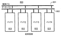
図8および9の説明
ダイナミックRAMは、複数のバンクとともに単一パッケージにパッケージングされている。バンクとは、別々にアドレス指定可能な1つの記憶ユニットのことである。バンクは物理パッケージ上のピンなどの入出力資源を共有するので、複数のバンクが同時に複数のアクセス要求を処理することができる。処理できる未解決要求の最大数は、クロック速度および同期SDRAMデバイスの構造によって決まる。近似的に、SDRAM内の1バンクへのアクセスが完了するのに4クロック・サイクルを要し、パッケージ内に4つまたはそれ以上のバンクがある場合、処理に4回のアクセスが同時に含まれる可能性がある。第1のアクセスを完了するのにかかわる4クロックのそれぞれの立ち上がりエッジで新しいアクセスが有効にされる。
Description of FIGS. 8 and 9 The dynamic RAM is packaged in a single package with multiple banks. A bank is a single storage unit that can be addressed separately. Since banks share input / output resources such as pins on a physical package, multiple banks can process multiple access requests simultaneously. The maximum number of outstanding requests that can be handled depends on the clock speed and the structure of the synchronous SDRAM device. Approximately, it takes 4 clock cycles to complete an access to one bank in the SDRAM, and if there are 4 or more banks in the package, the process can include 4 accesses simultaneously. There is sex. A new access is validated on each rising edge of the four clocks involved in completing the first access.
図8は、円803の中に4つのバンク810、811、812、および813を示している。これは、1つの可能なSDRAMの中の4つのバンクを表している。漏斗802および蛇口804は、SDRAMの中にあるものにアクセスするための共有制御およびデータ・バス資源を表す。4つのアクセス要求A、B、C、D(801)が、SRAM803の漏斗802に入る状況を示している。
FIG. 8 shows four
アクセス要求A、B、C、またはDのうち一度に1つだけが漏斗802に入ることができる。各バンク810〜813は、アクセスに他と同じだけ時間を要する。バンクが要求Aを開始し、その後、他のバンクが要求Bを開始すると、要求Aに対する結果は、要求Bからの結果の前に蛇口804から現れる。しかし、しばらくの間、1つのバンクが要求Aについて動作し、他のバンクは同時に要求Bについて動作する。
Only one of access requests A, B, C, or D can enter the
アクセスは、バンクの任意の組合せにより処理することができる。これらは、すべて、同じバンクにより処理するか、または異なるバンクにより処理することができる。いくつかのアクセスでは、そのアクセス自体のバンクとなるが、他のアクセスではバンクを共有する。アクセスのいくつかのグループでは、バンクがまったく使用されていない可能性がある。例えば、図9に示されているように、アクセスAおよびBは、同じバンク810により処理されるが、アクセスCは、バンク812により処理され、アクセスDは、バンク813により処理される場合がある。アクセスのグループを利用可能なバンクに分配するプロセスは、パーティション分割と呼ばれる。バンクの観点から、アクセスの回数は重要な情報であるが、それは、すべてのアクセスが一様な特質を持つからである。したがって、パーティションは、バンクへのアクセスの会計といえる。例えば、{4,0,0,0}は、4つのアクセスが単一バンクを占有し、他の3つのバンクは占有されていないことを意味する。図9では、パーティションは{2,1,1,0}である。
Access can be handled by any combination of banks. These can all be processed by the same bank or by different banks. For some accesses, it becomes the bank of the access itself, but for other accesses it shares the bank. In some groups of access, the bank may not be used at all. For example, as shown in FIG. 9, access A and B may be processed by the
図10〜13の説明
図10の同期ダイナミックRAM(SDRAM)は、4独立バンク・メモリ・アーキテクチャである。バンク毎に、オペレーションにはアクセス待ち時間、書き込みオペレーションの場合にピンからメモリ・アレイへの情報の送出、または読み出しオペレーションの場合にメモリ・アレイからピンへの情報の送出が伴う。また、メモリ内部のセンス・アンプが次の読み出しまたは書き込みサイクルを準備できるようにプリチャージ間隔も必要である。4つのバンクのそれぞれが利用可能である。4つのバンクはそれぞれ、専用のセンス・アンプを備えており、SDRAMの制御ポートおよびデータ・ポートについてのみアクセスの争奪が発生する。
Description of FIGS. 10-13 The synchronous dynamic RAM (SDRAM) of FIG. 10 is a four independent bank memory architecture. For each bank, the operation involves access latency, sending information from the pin to the memory array for write operations, or sending information from the memory array to the pins for read operations. Also, a precharge interval is required so that the sense amplifier within the memory can prepare for the next read or write cycle. Each of the four banks is available. Each of the four banks has a dedicated sense amplifier, and contention for access occurs only for the control port and data port of the SDRAM.
図10および11は、制御バス801がSDRAMのバンク1および2に向けられた活動を受け入れていることを示している。アクセス・コマンド「A」と図11の関連する読み出しコマンド「R」との間に待ち時間がある。また、読み出しコマンドとデータが利用できるまでの間にも待ち時間がある。さらに、アクセス・コマンドA1とA2との間に待ち時間がある。図11では、10ナノ秒のクロック・サイクルは、便宜上使用されている。全体的なサイクル時間は80ナノ秒である。SDRAMの4つすべての利用可能なバンクは、このときにアクセスできるが、どのバンクもこの時間間隔内では1回しかアクセスできない。このような待ち時間があるため、SDRAMは、パイプライン深さが4段であると言われる。衝突インスタンスの条件が満たされるためには、さらに80ナノ秒のメモリ・サイクルが必要である。衝突インスタンスは、使用中SDRAMメモリ・バンクへのアクセス・フロー・レギュレータの到着として定義される。例えば、図11のクロック・サイクル2でバンク1に対するアクセス要求が到着した場合、クロック・サイクル9までメモリには適用できないが、それは、バンク1に対する要求Aがクロック・サイクル1で到着しているからである。
FIGS. 10 and 11 show that
図12は、SDRAM 1203をバッファ記憶域として使用するハードウェア・リンク・リスト・プロセッサ1201およびサポートされている流れ毎に先頭、末尾、およびカウントを保持するテーブル記憶域用に小さな同期スタティックRAM 1207を示している。SDRAM 1203は、4つのSDRAM 1210、1211、1213、および1214を備える。リンク・リスト・プロセッサ1201では、クロック1、3、5、11、および15について図13に示されているように5つのアクセス要求のストリームが発生すると仮定する。第1の3つのアクセスA1、A2、およびA3は、異なるバンクに向かうのでパイプライン化することができるが、クロック11での第4のアクセスA2は、クロック3のアクセスA2を処理する使用中バンク2に進むので遅延させなければならない。
FIG. 12 shows a hardware linked
一般に、ランダムなアクセス・ストリームが存在する場合に発生する争奪の平均量は、4バンクSDRAMに対する基準としてみなすことができる。バンクは入出力ファシリティのみを共有するので、4バンクSDRAMへの1ブロック分のアクセスに対し重み付きの平均アクセス時間を計算するほうが簡単である。例えば、パーティション{3,1,0,0}を考察する。アクセスに(A、B、C、D)のラベルを付けた場合、可能なグループ分けとして、{(A,B,C),(D)},{(A,B,D),(C)},((A,C,D),(B)},および{(B,C,D),(A)}がある。選択された2つのバンクは、{1,2},{1,3},{1,4},{2,3},{2,4},または{3,4}とすることができる。 In general, the average amount of contention that occurs when there is a random access stream can be considered as a criterion for a 4-bank SDRAM. Since the bank shares only the input / output facility, it is easier to calculate the weighted average access time for one block access to the 4-bank SDRAM. For example, consider partition {3, 1, 0, 0}. If the access is labeled (A, B, C, D), the possible groupings are {(A, B, C), (D)}, {(A, B, D), (C) }, ((A, C, D), (B)}, and {(B, C, D), (A)} The two selected banks are {1, 2}, {1, 3}, {1, 4}, {2, 3}, {2, 4}, or {3,4].
3つからなる1つのパーティションと1つからなる1つのパーティションを2つのバンクにマッピングする2つの方法がある。例えば、パーティション{(A,B,C),(D)}を{1,2}にマッピングしようとした場合、バンク1を持つ(A,B,C)およびバンク2を持つ(D)、またはバンク1を持つ(D)およびバンク1を持つ(A,B,C)のいずれかがありえる。4*6*2=48であり、4つのアクセスを配置する方法は256通りあるため、パーティション{3、1、0、0}が生じる確率は、0.1875である。漂遊アクセスは、2つの衝突するアクセスの内側でパイプライン化することができ、したがって、完了するクロックの数は8*3=24となる。

表1は、それぞれの可能な分配について示されている関連するデータとともにアクセスを4メモリ・バンクに分配する様々な可能な方法に関係するデータを例示している。表1の第1欄では、様々なバンクへのアクセスが可能な様々な可能なパーティションの一覧を示している。表1の最上行は、第1のバンクが4つのアクセスを受け取り、残りバンクは何も受け取らないことを示している。第1欄2行目の分配は、3、1、0、0である。第1欄の下の行の分配は、4つのアクセスすべてが平等に各バンクに分配されていることを示す。第2欄は、その行の各分配の確率を示す。第3欄は、その機能を完了するのに要するクロック・サイクル数を示している。第4欄は、完了までの重み付き平均時間を示す。第1行については、第1のバンクへの4つすべてのアクセスの分配の確率は0.0156である。これは、完了までの重み付き平均時間が0.5であれば完了までに32クロック・サイクルを要する。下の行は、1,1,1,1の分配、0.0938の確率を持ち、重み付き平均時間1.3125で完了までに14クロック・サイクルを要する。この評価から、最も確率の高い分配は2、1、1、0であり、確率は0.5625であることがわかる。最もよい可能な分配は、下の行に示されており、確率は0.0938である。 Table 1 illustrates data relating to various possible ways of distributing access to four memory banks, with associated data shown for each possible distribution. The first column of Table 1 lists various possible partitions that can access various banks. The top row of Table 1 shows that the first bank receives 4 accesses and the remaining banks receive nothing. The distribution in the first column and the second line is 3, 1, 0, 0. The distribution in the row below the first column indicates that all four accesses are distributed equally to each bank. The second column shows the probability of each distribution in that row. The third column shows the number of clock cycles required to complete the function. The fourth column shows the weighted average time to completion. For the first row, the probability of distribution of all four accesses to the first bank is 0.0156. This requires 32 clock cycles to complete if the weighted average time to completion is 0.5. The bottom row has a distribution of 1,1,1,1 with a probability of 0.0938 and takes 14 clock cycles to complete with a weighted average time of 1.3125. From this evaluation, it can be seen that the distribution with the highest probability is 2, 1, 1, 0, and the probability is 0.5625. The best possible distribution is shown in the bottom row, with a probability of 0.0938.
表1の4つのバンクについて、4つのアクセスを完了するまでの合計重み付き平均時間は17.98クロックである。この数字は、4バンク・メモリへのアクセスの可能なすべての組合せについて完了までの重み付き時間の合計である。2つの10ナノ秒システム・クロックのパイプライン・クロックおよび16ビット幅バスを仮定すると、4バンクSDRAMに対する平均持続可能スループットは、1.24Gビット/秒であるが、それは各メモリのトランザクションが、それぞれにつき2クロックに対し16ビットを要するからである。争奪オーバーヘッドは28.5%である。この値は、アクセス完了までの平均時間とアクセス完了までの可能な最短時間との差をアクセス完了までの可能な最短時間で割るという計算で求められる。例えば、アクセス完了までの平均時間が50ナノ秒とし、アクセス完了までの可能な最短時間が40ナノ秒であったと仮定する。すると、オーバーヘッドは25%になる。
図13および14は、争奪状態でないアクセスと争奪状態であるアクセスとの差を例示している。
For the four banks in Table 1, the total weighted average time to complete four accesses is 17.98 clocks. This number is the sum of the weighted time to completion for all possible combinations of access to the 4-bank memory. Assuming two 10-nanosecond system clock pipeline clocks and a 16-bit wide bus, the average sustainable throughput for a 4-bank SDRAM is 1.24 Gbit / s, which means that each memory transaction This is because 16 bits are required for 2 clocks. The contention overhead is 28.5%. This value is obtained by a calculation of dividing the difference between the average time until access completion and the shortest possible time until access completion by the shortest possible time until access completion. For example, assume that the average time to access completion is 50 nanoseconds and the shortest possible time to access completion is 40 nanoseconds. Then, the overhead becomes 25%.
13 and 14 illustrate the difference between an access that is not in contention and an access that is in contention.
図14の説明
頻繁な争奪は設計の決定に影響を及ぼす。図14のタイミング図を考察する。ここで、メモリ・バンクへのアクセス・バスはスロット付きである。それぞれのアクセスには、読み出し間隔と書き込み間隔が設定されている。これらのアクセスは、メモリの制御バスのアイドル時間を最小限に抑えるためできる限り緊密にパックする必要がある。
Description of FIG. 14 Frequent contention affects design decisions. Consider the timing diagram of FIG. Here, the access bus to the memory bank has a slot. A read interval and a write interval are set for each access. These accesses should be packed as closely as possible to minimize the idle time of the memory control bus.
このようにしてアクセスを構造化することは、争奪でメモリの平均読み書きサイクル時間が実質的に増大するため意味のあることである。平均読み書きサイクル時間は最大読み書きサイクル時間程度なので、メモリの読み書きサイクル時間が最大となるようにシステムを設計するとより効率的である。少ない読み書きサイクルを使用して効率および動作速度を高めることは、争奪を管理するために必要なハードウェアのコストに見合わない。 This structuring of access is meaningful because contention increases the average read / write cycle time of the memory substantially. Since the average read / write cycle time is about the maximum read / write cycle time, it is more efficient to design the system so that the read / write cycle time of the memory is maximized. Increasing efficiency and operating speed using fewer read / write cycles is not commensurate with the hardware cost required to manage contention.
メモリは、バス速度で定義された速度でアクセス要求を受け付けることができるが、それは内部パイプライン設計によりそうするようにできるからである。しかし、争奪率28.5%では、争奪の少ないシステムとは反対に、争奪率がキューの深さに指数関数的に関係しているため、このシステムにおけるキュー操作が劇的に増える。様々なアクセス時間をサポートするこのキュー操作および状態制御装置は、一定の最大アクセス時間を予想するものと比べてかなり念入りである。例えば、一定の最大アクセス時間を持つ設計では、キューを必要とせず、全体にわたる状態制御はかなり単純である。アクセス時間が頻繁に変わる設計では、メモリを使用しているマシン内に複数のキュー、さらに争奪が発生したときにアプリケーションからこのマシンを起動、停止できるより精巧な状態ロジックを必要とする。 The memory can accept access requests at a speed defined by the bus speed because it can do so by an internal pipeline design. However, at a contention rate of 28.5%, the queue operation in this system increases dramatically because the contention rate is exponentially related to the depth of the queue, as opposed to a system with less contention. This queuing and state control device that supports various access times is quite elaborate compared to those that expect a certain maximum access time. For example, a design with a constant maximum access time does not require a queue and overall state control is fairly simple. Designs with frequently changing access times require multiple queues in the machine that is using the memory, and more sophisticated state logic that can start and stop this machine from the application when contention occurs.
図15および16の説明
図15に示されているように、8バンク分のSDRAMがあると仮定する。この場合、メモリは、図13に示されているSDRAMのサイズの半分のブロックにパーティション分割される。例えば、図13のバンク1を宛先とするアクセスは、今度は、図16のバンク1またはバンク2のいずれかに入る。図13のバンク2を宛先とするアクセスは、図16のバンク3とバンク4との間に分割される、などとなる。図13では、バンク2への第2のアクセスは、バンク2への第1のアクセスとの争奪状態を引き起こし、遅延が発生する。図16では、これらのアクセスのうちの第1のものがバンク3に向かうが、それらのアクセスのうち第2のものはバンク4に向かう。
Description of FIGS. 15 and 16 Assume that there are 8 banks of SDRAM as shown in FIG. In this case, the memory is partitioned into blocks that are half the size of the SDRAM shown in FIG. For example, an access destined for
図13および16を比較すると、争奪の解消により、図13のクロック13(A4)とクロック16(R4)との間のアイドル・ギャップが閉じられることがわかる。図16では、データ・バスは、クロック7からクロック16へ連続的に占有される。争奪は、アクセスのランダムな内向きストリームが与えられると、異なる組合せで発生することがある。争奪は、8つのバンクでは解消されないが、バンクの数が多くなるほど争奪の発生は減少する。
表2は、バンクの数を増やした場合に完了までの重み付き平均時間がどのように減少するかを示している。最大持続可能スループットでは再び、10ナノ秒のシステム・クロックと16ビット幅のデータ・バスを仮定している。 Table 2 shows how the weighted average time to completion decreases when the number of banks is increased. The maximum sustainable throughput again assumes a 10 nanosecond system clock and a 16-bit wide data bus.
パイプライン深さも、パフォーマンスに影響を与える。例えば、8バンク分のメモリがあるが、パイプラインの中には2段しかない場合、2回アクセス完了までの重み付き平均時間は6.25クロックである。この場合のオーバーヘッドは4.2%であり、最大持続可能スループットは1.51Gビット/秒である。争奪率は5%に低下するものとする。その後、平均アクセス時間は3.5ナノ秒である。これは、かなりバス・サイクル時間に近い。この結果は、図14および図16に示されているアクセス制御配置を比較してみるとわかる。図14では制御バス活動の密度が高い、つまり、図14の場合よりも1クロック当たりのランダム読み書きアクセスが多いということがわかる。 Pipeline depth also affects performance. For example, if there are 8 banks of memory but there are only 2 stages in the pipeline, the weighted average time until the completion of the 2nd access is 6.25 clocks. The overhead in this case is 4.2% and the maximum sustainable throughput is 1.51 Gbit / s. The contention rate will drop to 5%. Thereafter, the average access time is 3.5 nanoseconds. This is very close to the bus cycle time. This result can be seen by comparing the access control arrangements shown in FIGS. FIG. 14 shows that the density of control bus activity is high, that is, there are more random read / write accesses per clock than in the case of FIG.
図17および18の説明
本発明では、独立連携状態コントローラ1804はRAMパッケージのそれぞれのバンク1803に割り当てられている。それぞれのバンクは、独立にサイクル動作し、その状態コントローラ1804を通じて、他のRAMバンク1803にあわせよく調整された形で結果を出すことができる。さらに、状態コントローラ1804の流れにより、ときおり発生する争奪のためにアクセス要求を保持するアクセス・フロー・レギュレータ1801のキューを制御する。これにより、アクセス要求の破棄が防止される。状態コントローラ1804は、さらに、バンク1803のリフレッシュなどのハウスキーピング機能を独立に管理する。状態コントローラ1804は、独立している。状態コントローラ1804を使用すると、RAMバンク1803との間のバックグラウンド・バースト転送を、他のRAMバンク1803のフォアグラウンドのアクセス活動と同時に行うようにできる。このため、RAMバンク1803からリンク・リストの中間部をリモートRAM1806に格納することができる。これにより、リンク・リストの先頭および末尾のみがRAMバンク1803に残る。例えば、図6のキュー506を見ると、バッファQおよびZは、RAMバンク1803内のどこかに置かれるが、バッファDおよびRは、リモートRAM1806内に格納される。リンク・リストの中間をリモートで格納できれば、開示されているシステムでは、市販のパッケージRAMを使用して任意のサイズのリストをサポートすることができる。リンク・リストの大部分をリモートRAM1806にリモートで格納することができる場合、FPGAに埋め込まれているRAM1803を先頭と末尾に使用することができる。状態コントローラ1804は、先頭と末尾を保持するRAM1803と組み合わせる。この設計は、RAM 1803と異なるパッケージに常駐する状態コントローラよりも効率がよい。RAM 1803と状態コントローラとが同じ場所にある場合は、リストの先頭と末尾を格納するため技術を選択することになる。この選択結果は、少数のリンク・リスト・キュー用のオンボード・レジスタ、適度の量のリンク・リスト・キューのスタティックRAM 1803、または大量のリンク・リスト・キューのダイナミックRAM 1806である。
Description of FIGS. 17 and 18 In the present invention, the independent
状態コントローラ1804のブロック図が図17に示されている。
状態コントローラ1804は、フォアグラウンド・ポートから流れ込む情報をゲートするアービトレーションおよびシーケンシング・ロジックが適用され、フォアグラウンドまたはバックグラウンド転送で使用中の場合に新しい着信活動を行わないようにRAMメモリ・バンク1803をガードする。さらに、状態コントローラは、RAMメモリ・バンク1803内の状態を監視し、リモートRAM1806との相互作用が発生する場合にそれを判別する。状態コントローラ1804は、図18に示されているように、バンクグラウンド・アクセス・マルチプレクサ1808、リモートRAM 1806、およびアクセス・フロー・レギュレータとともにシステム内に組み込まれる。
A block diagram of
The
図17の状態コントローラ1804は、関連するRAMメモリ・バンク1803、アクセス・フロー・レギュレータ1801、およびバックグラウンド・アクセス・マルチプレクサ1808の間のインターフェースとして機能する。これらの要素への接続は、図17に詳しく示されている。状態コントローラ1804は、マルチプレクサ1702ならびにアービトレーションおよびシーケンシング・ロジック要素703を備える。低位側では、マルチプレクサ1702は、経路1710および1711に接続され、図18のバス1809−1〜1809−9の一部となる。この経路の上で、マルチプレクサは読み出しおよび書き込みオペレーションで経路1710を介して関連するRAMメモリ・バンクとデータを交換する。経路1711は、マルチプレクサ1702を介して状態コントローラ1804が関連するRAMメモリ・バンク1803のオペレーションを制御することを可能にする双方向制御経路である。RAMデータ経路1710は、マルチプレクサを介してデータ経路1704またはバックグラウンド・アクセス・マルチプレクサ1808に届くデータ経路、またはデータ経路1705およびバス1802を介してアクセス・フロー・レギュレータ1801に接続することができる。これらのデータ経路は、読み出しオペレーションと書き込みオペレーションの両方で使用することができる。
The
マルチプレクサ1702の底部のRAM制御経路1711は、経路1712ならびにアービトレーションおよび制御ロジック要素1703を介して経路1707および1706に接続されている。マルチプレクサの経路1711は、一度に経路1707および1706の一方のみに接続可能である。経路1706に接続された場合、さらに経路1810におよび、読み出しと書き込み両方のオペレーションでバックグラウンド・アクセス・マルチプレクサ1808および関連するリモートRAM 1806のオペレーションを制御する。経路1711が要素1703を介して経路1707に接続された場合、さらに、バス1802を介してアクセス・フロー・レギュレータ1801に及ぶ。アービトレーションおよびシーケンシング・ロジック要素1703は、読み出しおよび書き込みの両方のオペレーションで状態コントローラ1804とのデータ交換後、アクセス・フロー・レギュレータ1801を制御するために必要な情報処理機能およびロジック機能を備える。アービトレーションおよびシーケンシング・ロジック1703はさらに、バス1706および1810を介して、バックグラウンド・アクセス・マルチプレクサ1808と通信し、リモートRAM1806がRAMメモリ・バンク1803からデータを受け取ったときのオペレーションだけでなくリモートRAM 1806がデータを状態コントローラ1804に送信し、状態コントローラに関連付けられたRAMメモリ・バンクに入力するオペレーションを制御する。
The RAM control path 1711 at the bottom of
状態コントローラ1804は、関連するRAMメモリ・バンク1803と、およびアクセス・フロー・レギュレータ1801と、およびバックグラウンド・アクセス・マルチプレクサ1808を介してリモートRAM 1806と制御およびデータを交換する4つの高水準機能を備える。これら4つの高水準機能について次に説明する。
The
図17の状態コントローラ1804によって実行される第1の機能は、読み出しまたは書き込み要求が発生したときにアクセス・フロー・レギュレータ1801からの情報の転送に関連する内向きアクセス要求シーケンスを開始し、制御し、そうする際に、関連するRAMメモリ・バンク1803を制御し、書き込み要求ではデータをRAMメモリ・バンク1803に書き込み、アクセス・フロー・レギュレータ1801からの読み出し要求ではRAMメモリ・バンク1803からデータを読み出すことである。
The first function performed by the
図17の状態コントローラにより実行される第2の機能は、関連するRAMメモリ・バンク1803内のバッファ満杯レベルを検出するトリガ信号に応答することである。このトリガは、関連するRAMメモリ・バンク内のバッファが十分に消費されたか枯渇したことを示す。関連するRAMメモリ・バンク内のバッファが十分に消費されている場合、リモートRAM 1806への書き込みがトリガされる。関連するRAMメモリ・バンク内のバッファが十分に枯渇している場合、リモートRAM 1806からの読み出しがトリガされる。 A second function performed by the state controller of FIG. 17 is in response to a trigger signal that detects a buffer full level in the associated RAM memory bank 1803. This trigger indicates that the buffer in the associated RAM memory bank has been fully consumed or depleted. If the buffer in the associated RAM memory bank is fully consumed, writing to the remote RAM 1806 is triggered. If the buffer in the associated RAM memory bank is sufficiently depleted, a read from the remote RAM 1806 is triggered.
状態コントローラ1804により実行される第3の機能は、関連するRAMメモリ・バンク1803からリモートRAM 1806への転送を開始し、管理し、さらに、リモートRAM 1806からRAMメモリ・バンク1803に戻る逆の方向のデータ転送も管理することである。
The third function performed by the
状態コントローラ1804により実行される第4の機能は、マルチプレクサ1702からの信号を待ち、マルチプレクサ1702からその信号を受信した後リモートRAM 1806との間の転送を開始することである。
A fourth function performed by the
マルチプレクサ1702により実行される他の機能は、複数のRAMメモリ・バンク1803が同時にリモートRAM 1806へのアクセス権を要求している場合にリモートRAM 1806へのアクセス権をどのビッディングRAMメモリ・バンク1803に与えるかを選択することである。マルチプレクサ1702により実行される他の機能は、リモートRAM 1806とビッディングRAMメモリ・バンク1803との間のオペレーションに関連する転送およびスケジューリング機能を、前記転送の間に依存関係がある場合に、開始することである。このような依存関係は、メモリ・システムとの間のストリーミング化されたアクセスから生じることがある。
Another function performed by
マルチプレクサ1702により実行されるさらに他の機能は、RAMメモリ・バンク1803を制御し、リモートRAM 1806からの書き込み入力の方向を決めることである。マルチプレクサ1702は、リモートRAM 1806へのアクセス権を与え、リモートRAM 1806とRAMメモリ・バンク1803との間の情報の経路を設定する。
Yet another function performed by
表2は、RAMバンク1803争奪があると、従来のSDRAMに基づくシステムのパフォーマンスが制限される場合があることを示している。図14の説明から、この制限は厳しいため、システムはRAMメモリ・バンク争奪を回避して設計されていることがわかる。図14の設計では、RAMバンクの利用可能性を予想することに基づく争奪とは反対にRAMメモリの全サイクル時間の時間間隔についてアクセスを構造化することによりすべてのサイクルでの争奪を回避している。つまり、RAMメモリ・バンクは設計上、最適な速度よりも遅い速度で動作するということである。図12および13は、バンクの利用可能性を予想するシステムを説明しているが、争奪が発生した場合のために実質的によけいなロジックを必要とする。この実装の問題は、争奪によりパフォーマンスが奪われ、必要なハードウェアを追加したとしても十分なパフォーマンス向上がないという点である。 Table 2 shows that the contention of a RAM bank 1803 may limit the performance of a conventional SDRAM-based system. From the description of FIG. 14, it can be seen that this limitation is severe and the system is designed to avoid contention for RAM memory banks. The design of FIG. 14 avoids contention in all cycles by structuring access for the time interval of the total cycle time of RAM memory as opposed to contention based on predicting RAM bank availability. Yes. That is, the RAM memory bank is designed to operate at a speed slower than the optimum speed. FIGS. 12 and 13 describe a system that anticipates bank availability, but requires substantially good logic in case a stake occurs. The problem with this implementation is that performance is lost due to contention, and even if the necessary hardware is added, there is not enough performance improvement.
図15および16は、RAMメモリ・バンクの数を増やして争奪回数を減らすことによるオペレーションの向上を示している。これには、ハードウェアのロジックを増やす必要がある。パフォーマンスの向上とハードウェアの増大との関係は、ハードウェアを受け入れられるだけ追加するとパフォーマンスの違いが目立ってわかるというような関係である。多数のRAMメモリ・バンクへのアクセスを調整するには、図17に示されているような専用の状態ロジックが必要であり、ハードウェア資源が消費される。これらの資源は、市販のFPGAの中から見つけられる。パフォーマンスを最大にするためには、マスカブル・データ・バスが好ましい。バースト・データを滑らかに吸収するために広くなければならず、また最小クオンタムのデータを格納しやすくするためにマスク可能でなければならない。このようにして構成可能なメモリは、市販のFPGAで利用可能である。しかし、このメモリは、前述のように、300ミリ秒分のOC−768オプション・ファイバのバッファリングなど、実質的なバッファリング・ジョブには不十分な小さな量でしか利用できない。さらに、集積回路内では利用可能な領域の量は限られている。RAMメモリに使用される領域は、状態コントローラ・ロジックには使用できず、その逆もそうである。しかし、RAMバンクを増やすと、パフォーマンスが向上し、各バンクは専用の状態コントローラを持たなければならない。したがって、バッファリング要件を満たすこととシステムのパフォーマンスとの間には食い違いがある。 FIGS. 15 and 16 illustrate the improvement in operation by increasing the number of RAM memory banks and reducing the number of contendings. This requires more hardware logic. The relationship between improved performance and increased hardware is that the difference in performance is noticeable when hardware is added as much as it can accept. Coordinating access to multiple RAM memory banks requires dedicated state logic as shown in FIG. 17 and consumes hardware resources. These resources can be found in commercially available FPGAs. A maskable data bus is preferred for maximum performance. It must be wide to absorb burst data smoothly, and it must be maskable to make it easier to store minimum quantum data. A memory that can be configured in this manner can be used in a commercially available FPGA. However, this memory is only available in small quantities that are not sufficient for substantial buffering jobs, such as 300 milliseconds of OC-768 optional fiber buffering, as described above. Furthermore, the amount of available area within an integrated circuit is limited. The area used for RAM memory is not available for state controller logic and vice versa. However, increasing the number of RAM banks improves performance and each bank must have a dedicated state controller. Thus, there is a discrepancy between meeting buffering requirements and system performance.
このコンフリクトに対する解決策は、FPGA RAMバンク1803に載せるメモリの量を制限することである。リンク・リストの先頭および末尾のみがアクセスされ、リンク・リストの中間の要素は、リストの先頭に移動するまで、常にアイドル状態である。したがって、リンク・リストの中間要素をボードから移動して離し、FPGA RAMバンク1803からリモートRAM 1806に移すと、パフォーマンスを向上させることができる。 The solution to this conflict is to limit the amount of memory on the FPGA RAM bank 1803. Only the top and bottom of the linked list are accessed, and the middle elements of the linked list are always idle until moving to the top of the list. Therefore, performance can be improved if the intermediate elements of the linked list are moved away from the board and moved from the FPGA RAM bank 1803 to the remote RAM 1806.
この妥協策を実装するシステムは、図17および18に示されている。
この解決策は、経済的な理由からも賢明な方法である。RAMメモリの構成可能なバンクは、1ビット当たりの価格が市販のSDRAMに比べてかなり高い。リンク・リストの中間要素を保持するリモートRAM 1806がアクセスされていなければ、そのメモリに関連するサイクル時間ペナルティはない。最終的には、リモートRAM 1806にアクセスして、リストの中間への要素の格納および取得を行わなければならない。しかし、FPGA上のメモリの多数のバンクには上述の構成可能な性質があるため、SDRAM RAMバンク1803のバースト・モードと互換性のある設計が可能である。メモリの多数のバンクからなるシステムのスループットをSDRAMに一致させ、バランスのとれた設計とすることも可能である。これにより、SDRAM 1803をバースト・モードで動作させ、データ・バス上でクロックと同期がとられているデータとともにサイクル時間をパイプライン化して、SDRAMサイクル時間のコストを最小限に抑えることができる。これで、同様に、メモリはメモリが当初設計された動作モードに戻る。
Systems that implement this compromise are shown in FIGS.
This solution is also sensible for economic reasons. A configurable bank of RAM memory has a significantly higher price per bit than a commercially available SDRAM. If the remote RAM 1806 that holds the intermediate elements of the linked list has not been accessed, there is no cycle time penalty associated with that memory. Eventually, the remote RAM 1806 must be accessed to store and retrieve elements in the middle of the list. However, because of the configurable nature of the many banks of memory on the FPGA, a design compatible with the burst mode of the SDRAM RAM bank 1803 is possible. It is also possible to have a balanced design by matching the throughput of a system consisting of multiple banks of memory to SDRAM. This allows SDRAM 1803 to operate in burst mode and pipeline the cycle time with data that is synchronized with the clock on the data bus to minimize the cost of the SDRAM cycle time. This similarly returns the memory to the mode of operation in which the memory was originally designed.
リンク・リスト・バッファは、バックグラウンド・アクセス・マルチプレクサ1808を介してリモートRAM 1806に置いたり、取り出したりされる。このため、フォアグラウンド・アクセスを、この追加トラフィックに関係なく、進められる。これは、表2に例示されている確率論的モデルが図18に示されているように利用可能なフォアグラウンド・バスに依存しているため重要である。フォアグラウンド・バス1810で進行中のリモートRAM 1806へのバックグラウンド転送をブロックすると、表2を得るために使用されるモデルはかなり込み入ったものとなる。したがって、パフォーマンスが低下する。バックグラウンド・アクセス・バス1810が示されている。
The link list buffer is placed in and retrieved from the remote RAM 1806 via the
図18は、本発明を具現化するリンク・リスト・エンジン1800を開示している。リンク・リスト・エンジン1800は、ポート1817および1818に接続されている着信経路1812および送信経路1813を持つ通信システム1811に接続されていることが示されている。このシステムは、プロセッサ1814を備え、さらに、経路1819を介してアクセス・フロー・レギュレータ1801にまで及ぶ経路1815および1816も含む。動作すると、システム1811はリンク・リスト・エンジン1800のメモリを使用して読み出しおよび書き込みオペレーションを実行し、動作中にポート1817および1818で必要とするデータを格納する。
FIG. 18 discloses a linked
アクセス・フロー・レギュレータ1801およびバス1802は、複数の状態コントローラ1804に接続されるが、それぞれ複数のRAMメモリ・バンク1803のうちの1つと関連付けられている。アクセス・フロー・レギュレータ1801は、RAMメモリ・バンク1803の1つに情報を格納するよう要求する書き込み要求をシステム1811から受け取る。アクセス・フロー・レギュレータ1801は、それらのアクセス要求を受け取って格納し、データを関連するRAMメモリ・バンク1803に入力するため様々な状態コントローラ1804に選択的に分配する。このプロセスは、アクセス・フロー・レギュレータ1801がシステム1811から読み出し要求を受け取ったときにメモリ読み出しオペレーションで逆の方向に動作し、このプロセスにより、状態コントローラ1804を介して、要求されたデータを含むRAMメモリ・バンク1803が読み出され、状態コントローラ1804およびバス1802を介して、システム1811にデータを送信するアクセス・フロー・レギュレータに適用される。
RAMメモリ・バンク・デバイス1803は、RAMメモリ・バンク1803から情報を受け取り、その情報がRAMメモリ・バンクですぐに必要ない場合に格納しておくことができるリモートRAM 1806により増強された比較的小さなメモリ記憶容量を持つ高速な要素である。リモートRAM1806は、動作中、バックグラウンド・アクセス・マルチプレクサ1808およびパス経路1810により補助され、マルチプレクサおよびパス経路はそれぞれ一意的な状態コントローラ1804および関連するRAMメモリ・バンク1803にまで及んでいる。この手段により、満杯または空になりつつあるRAMメモリ・バンク1803は、このことを関連する状態コントローラ1804に通知し、このコントローラはさらに、バス経路810を介してバックグラウンド・アクセス・マルチプレクサ1808と通信することができる。マルチプレクサ1808は、状態コントローラ1804がRAMメモリ・バンク1803から情報を読み出して、リモートRAM 1806に転送し、その情報が出所のRAMメモリ・バンク1803によって再び必要になるまで一時的記憶域に置く動作を補助する。このときに、RAMメモリ・バンク1803は、状態コントローラ1804に、リモートRAM1806がRAMメモリ・バンクによって必要になりそうな情報を含んでいることを通知する。バックグラウンド・アクセス・マルチプレクサ1808および状態コントローラ1804を連携動作し、それにより、リモートRAM1806の適切な部分は情報を読み出して出所のRAMバンク1803に送り返す。リモートRAM1806は、比較的低速の大容量メモリ要素であり、RAMメモリ・バンク1803からオーバーフローする情報を効率よく格納するか、または情報をアンダーフローになったRAMメモリ・バンク1803に供給することができる。
The RAM memory bank device 1803 receives information from the RAM memory bank 1803 and is relatively small augmented by a remote RAM 1806 that can store the information if it is not immediately needed in the RAM memory bank. It is a high-speed element with memory storage capacity. In operation, the remote RAM 1806 is assisted by a
本発明の一態様は、図18の方法および装置を含み、そこでは、RAMメモリ・バンク1803への書き込みオペレーションは状態コントローラ1804を介してリンク・リスト情報をRAMメモリ・バンク1803に書き込む工程と、満杯状態に近づくまでRAMメモリ・バンク1803への書き込みオペレーションを継続する工程と、状態コントローラ1804およびバックグラウンド・アクセス・マルチプレクサ1808を介してRAMメモリ・バンク1803から新規に受信された情報の一部を同時にリモートRAM 1806に読み出しながらアクセス・フロー・レギュレータ1801からRAMメモリ・バンクに追加情報を書き込むことを継続する工程とにより実行される。この情報は、その後出所のRAMメモリ・バンク1803により必要になるまでリモートRAM1806内に残される。
One aspect of the present invention includes the method and apparatus of FIG. 18, wherein a write operation to RAM memory bank 1803 writes link list information to RAM memory bank 1803 via
図18のシステムは、RAMメモリ・バンク1803からのデータの読み出しを実行するが、そのために、要求されたデータを含むRAMメモリ・バンク1803と関連付けられた状態コントローラ1804に信号を送る工程と、状態コントローラ1804およびバス1802を介して選択されたデータの読み出し結果をアクセス・フロー・レギュレータ1801に戻すことを開始する工程と、選択されたRAMメモリ・バンク1803の読み出しを継続し、それと同時に、それらの読み出しで注目するデータの選択されたRAMメモリ・バンク1803が尽きてしまったこと、およびその後の読み出しオペレーションで必要となる注目するデータの一部が現在、リモートRAM 1806に格納されていることを判別する工程とを使用する。リモートRAM1806からプリフェッチ読み出しを開始し、情報を要求される前に出所のRAMメモリ・バンク1803に転送して戻す工程と、選択されたRAMメモリ・バンク1803の読み出しを継続し、必要ならば、リモートRAM1806から読み出し中のRAMメモリ・バンク1803へのデータの読出しを継続する工程とを使用する。このオペレーションは、読み出しオペレーションについてアクセス・フロー・レギュレータ1801により要求された情報全部が履行されるまで継続される。
The system of FIG. 18 performs a read of data from the RAM memory bank 1803, for this purpose, signaling a
RAMメモリ・バンク1803の高速メモリ・デバイスおよびリモートRAM 1806の低速大容量メモリは連携動作し、高速RAMメモリ・バンク1803の容量を超えるデータを格納する。リモートRAM 1806は、書き込み中のRAMメモリ・バンクからの書き込みオペレーションでこのデータを受け取るが、その一方で、RAMメモリ・バンク1803はアクセス・フロー・レギュレータ1801から高速でさらにデータを受信し続けることができる。このプロセスは、RAMメモリ・バンク1803が最初に高速で読み出されると逆方向に読み出しオペレーションで動作し、RAMメモリ・バンクで必要とされリモートRAM 1806に格納されるデータは、RAMメモリ・バンク1803に注目する情報が枯渇すると、プリフェッチ方式でRAMメモリ・バンク1803に転送して戻される。読出しオペレーションは継続し、リモートRAM1806内の関連情報すべてを高速RAMメモリ・バンク1803に転送して戻すことができ、アクセス・フロー・レギュレータ1801により要求された情報全部が状態コントローラ1804およびバス1802を介して高速なRAMメモリ・バンク1803によりアクセス・フロー・レギュレータ1801に送り返されるまで高速データ転送速度で読み出される続ける。または、状態コントローラ1804およびRAMメモリ・バンク1803は、バックグラウンドでの取得をトリガした前回の読み出しオペレーションと別の書き込みオペレーションを続行することができる。プリフェッチはトリガにより自動実行されるため、特定の状態コントローラ1804およびRAMメモリ・バンク1803がバックグラウンド転送で占有されている間、他の状態コントローラ1804およびRAMメモリ・バンク1803は自由に、このバックグラウンド・オペレーションとは無関係にオペレーションを実行できる。
The high-speed memory device of the RAM memory bank 1803 and the low-speed large-capacity memory of the remote RAM 1806 operate in cooperation to store data exceeding the capacity of the high-speed RAM memory bank 1803. The remote RAM 1806 receives this data on write operations from the RAM memory bank being written, while the RAM memory bank 1803 may continue to receive more data from the
本発明の他の態様では、状態コントローラ1804を使用して経路1820を介して電位をアクセス・フロー・レギュレータ1801に印加し、それぞれの状態コントローラ1804に関連付けられているRAMメモリ・バンク1803が既存の読み出しまたは書き込みオペレーションで現在使用中かどうか、または新しい読み出しまたは書き込みオペレーションの受信された要求に利用可能かどうかを示す。RAMメモリ・バンク・デバイス1803のメモリ要素は光バスの高速データ転送速度で動作するので、RAMメモリ・バンク1803は、光ファイバ・バスに適した速度で読み出しまたは書き込みオペレーションを実行することができる。その結果、経路1820を経由して状態コントローラにより使用中信号がアクセス・フロー・レギュレータ1801に印加され、関連するRAMメモリ・バンクが利用可能である、または利用可能でないことを示す。この信号は、読み出しまたは書き込みオペレーションを実行するためにRAMメモリ・バンク1803デバイスに必要な数ナノ秒間しか持続しない。したがって、状態コントローラ1804によりこの使用中/アイドル電位が経路1820に印加される場合、争奪ファシリティによりアクセス・フロー・レギュレータ1801およびその要素1821はRAMメモリ・バンク1803の使用中/アイドル状態を監視することができる。このため、読み書きでの任意の所定の最小時間間隔をRAMメモリ・バンク1803に課す従来技術の複雑なロジック回路要素または争奪配置による争奪の遅延は解消される。この手段により、アクセス・フロー・レギュレータ1801、経路1820、および状態コントローラ1804は、光ファイバ・バスのナノ秒転送速度で動作する効率的で高速な争奪ファシリティを実現する。この改善された高速な争奪配置では、ポート1817および1818に関連付けられた着信および送信キューはRAMメモリ・バンク1803の高速要素により処理されるためより高速にデータを交換し処理することができるので、システム1811により処理されるデータのスループットを高めることができる。したがって、図18のリンク・リスト・エンジン1800は、光ファイバ・リンクと同じ速度でポート1817および1818により必要とされるデータ・キューの読み書きを実行することができる。
In another aspect of the invention, the
図19の説明
図19は、5つのバッファ1から5を含む標準的なリンク・リストを開示している。これら5つのバッファのリンク・リストは、図18の同じRAMバンク1803上には格納されない。その代わりに、これら5つのバッファは、5つの別々のバンク1803にランダムに格納される。それぞれのバッファは、システムによって格納され処理される物理的情報またはデータを含む第1の部分を持つ。各バッファの下位部分は、リンク・リストの次のバッファを格納するRAMバンクへのリンク・フィールド・アドレスを含む。図19のバッファ1は、上位部分に物理的情報を格納し、下位部分に0100のリンク・フィールド・アドレスを格納する。バッファ1を格納するRAMバンクのアドレスは、バッファ1の右に示されているように000/00である。
Description of FIG. 19 FIG. 19 discloses a standard linked list containing five
リンク・リストのバッファ2は、バッファ1のリンク・フィールドで指定されているようにRAMアドレス01/00に格納される。バッファ2の最上位部分は、物理的情報(データ)を含む。下位部分は、RAMバンクIDおよびリンク・リストのバッファ3を格納する場所を指定する01001のリンク・フィールド・アドレスを含む。
バッファ3は、バッファ2のリンク・フィールドによって指定されているようにRAMバンク・アドレス010/01に格納される。バッファ3のリンク・フィールドは、リンク・リストの第4のバッファの場所を指定する11010のアドレスを含む。
第4のバッファは、バッファ3のリンク・フィールドによって指定されているようにRAMアドレス110/10に格納される。同様に、リンク・リストの第5のバッファおよび最後のバッファは、バッファ4のリンク・フィールドによって指定されているようにRAMアドレス101/11に格納される。バッファ5の最上位部分は、使用できる自由リストの先頭バッファであることを示す。
The fourth buffer is stored at RAM address 110/10 as specified by the link field of
リンク・リスト上のバッファは、図18の別のRAMバンク上にランダムに格納される。このランダム性は、システムのデータ処理および制御オペレーションを効率よく行う上で望ましく、また必要である。このランダム性は、本発明の争奪ファシリティの所望のオペレーションを実現するために特に必要であり有用である。 Buffers on the linked list are randomly stored on another RAM bank in FIG. This randomness is desirable and necessary for efficient data processing and control operations of the system. This randomness is particularly necessary and useful for realizing the desired operation of the contention facility of the present invention.
図20および21の説明
図20は、RAMメモリ・バンク1803内のリンク・リスト・キューの先頭がどのように枯渇し、大容量RAMメモリ1806のアクセスを必要とするかを示している。図に示されているリンク・リスト・キューは、それぞれの順序で、内容Q、F、R、およびZを含むバッファを持つ。図21では、クロック期間A1の第1のアクセスで、RAM1803から図21のクロック期間7および8の内容Qを保持するアドレスを読み出す。しかし、アクセスA1により、使用するキューの先頭が高速メモリ1803から取り出され、リモートRAM 1806に次の要素Fが格納される。したがって、アクセスA1により、アクセスA1にかかわるRAMバンク1803の状態コントローラ1804を通じてクロック期間2でバックグラウンド要求Rq1がトリガされる。このリモート・メモリ1806アクセス要求は、バックグラウンド・アクセス・マルチプレクサ1808により処理され、図21のクロック期間3でリモート・メモリ・アクセスA1Bによって返される、リモートRAM 1806はRAMバンク1803へのアクセスの流れと同時に発生することに注意されたい。データD1Bは、クロック期間9および10でリモートRAM 1806から消費される。このデータはリンクされたリスト要素Fである。要素Fは、アドレスがRAMバンク5内にある自由リストから取り出された空要素に書き込まれ、アクセスA5はクロック・サイクル11で始まる。リンクは全体を通して保存される。したがって、キューの先頭は、要素Fを含み、再び、ハイパフォーマンスRAMバンク1803〜1805に置かれる。要素Qを保持しているRAMバンク1803〜1805および内容Fを以前保持していたリモート・メモリ要素は、それぞれの自由リストに戻される。
ハイパフォーマンスRAM 1803へのアクセスが無相関であるという性質は温存され、表2に至るモデルはそのままとなるだけでなく、アクセス制御のギャップを作ることがないことにより図20に示されているように、より効率的に利用できるのではないかという期待が持続する。ギャップは争奪によって生じるという前の議論を思い出そう。相関のあるトラフィック、つまり同じバンクへの順次アクセスが争奪を引き起こすということである。
Description of FIGS. 20 and 21 FIG. 20 shows how the head of the link list queue in RAM memory bank 1803 is depleted and requires access to mass RAM memory 1806. The linked list queue shown in the figure has a buffer containing the contents Q, F, R, and Z in each order. In FIG. 21, the address that holds the contents Q of the
The nature of uncorrelated access to the high performance RAM 1803 is preserved, not only leaving the model leading to Table 2 intact, but also creating no access control gaps as shown in FIG. The expectation that it can be used more efficiently will continue. Recall the previous argument that the gap is caused by contention. Correlated traffic, ie sequential access to the same bank, causes contention.
図22の説明
図22は、バッファが図18の様々なRAMバンク1803−1から1803ー8(これ以降RAMバンク1803)にランダムに格納されるリンク・リストの読み出しを要求するアクセス・フロー・レギュレータ1801によって開始される読み出し要求を実行する本発明のプロセスを開示している。アクセス・フロー・レギュレータ1801が読み出しオペレーションを要求するプロセッサ1814から命令を受け取ったときに工程2201でプロセスが開始する。リンク・リストの個別バッファが一度に1つずつ順次読み出され、複数のRAMバンク1803のうち様々なバンクにランダムに格納される。各バッファの読み出しには、アクセス・フロー・レギュレータ1801による別々の読み出し要求が必要である。
Description of FIG. 22 FIG. 22 is an access flow regulator that requires the buffer to read a linked list that is randomly stored in various RAM banks 1803-1 through 1803-8 (hereinafter RAM bank 1803) of FIG. The process of the present invention for executing a read request initiated by 1801 is disclosed. The process begins at
第1の読み出し要求は、工程2202で受け取られ、工程2203に進み、そこで、RAMバンク1803から読み出される要素の個数に関してしきい値を超えたかどうかを判別する。すでに述べたように、リンク・リストの読み出しでは、先頭バッファが格納されているRAMバンク1803からリストの初期バッファ(先頭)を読み出す必要がある。リンク・リストの実行の残り部分で、リンク・リストの中間バッファを読み出す必要があり、それらをリモートRAM 1806に格納し、また取り出してRAMバンク1803に格納しなければならない。リモートRAM 1806からRAMバンク1803にバッファを戻す効率よい転送には、そのような複数の要求をバックグラウンド・アクセス・マルチプレクサ1803に適用し、次に、その工程の実行時に効率のためリモートRAM 1806に適用する必要がある。このような理由から、しきい値検出要素2203を用意し、個別に一度に1つずつではなく同時にそのような複数の要求をリモートRAM1806に送るようにする。
The first read request is received at step 2202 and proceeds to step 2203 where it is determined whether a threshold has been exceeded for the number of elements read from the RAM bank 1803. As described above, when reading the link list, it is necessary to read the initial buffer (head) of the list from the RAM bank 1803 in which the head buffer is stored. For the remainder of the linked list execution, the linked list intermediate buffers must be read and stored in the remote RAM 1806 and retrieved and stored in the RAM bank 1803. For efficient transfer of buffers back from the remote RAM 1806 to the RAM bank 1803, such multiple requests are applied to the background access multiplexer 1803 and then to the remote RAM 1806 for efficiency during execution of the process. Need to apply. For this reason, the
最初に、要素2203がしきい値を超えていないことを判別すると仮定しよう。この場合、リモートRAM 1806は即座にアクセスされず、プロセスは工程2204に進み、リンク・リストの第1のバッファ(先頭)の読み出し要求により識別されたRAMバンクを読み出す。このバッファの位置は、読み出され、一時的に格納され、プロセスは工程2205に進み、そこで、読み出された情報をアクセス・フロー・レギュレータ1801に返す。次に、このプロセスは、工程2206に進み、RAMバンク1803がアクセス・フロー・レギュレータ1801から次のアクセス要求を受け取る準備ができていることを示す。末尾バッファも、リンク・リストがただ1つのバッファで構成されている場合と同じように読み出される。
First, assume that it is determined that
次に、要素2203は、工程2202の新着読み出し要求により、読み出しオペレーションにRAMバンク1803内で利用可能なバッファの数に関してしきい値を超えたかどうかを判別すると仮定しよう。この場合、工程2211では、先頭バッファを読み出し、工程2220にさらに進み、工程2211の読み出し情報をアクセス・フロー・レギュレータ1801に送信する。次に、工程2221では、読み出すRAM 1806内のリストの先頭付近にある中間バッファの読み出しを要求する。これは、リストの先頭の要求を含む。そうする際に、工程2221は、リストの新しい先頭バッファの読み出し要求を、指定されたRAMバンク1806を処理するバックグラウンド・アクセス・バス1810に出す。次に、工程2222では、リモートRAM 1806からリストの複数の中間バッファを取り出す。次にこのプロセスは、工程2223に進み、リモートRAM 1806が別のアクセスの実行準備ができていることを示す。このプロセスはさらに、工程2212に進み、そこで、RAMバンク1803に、指定されたRAMバンク1803に書き込まれた工程2222中に読み出されたリモートRAM 1806の情報を書き込む。この情報は、指定されたRAMバンク1803内のリストの新しい先頭バッファの形成を含む。このプロセスは、次に、工程2205に進み、情報をアクセス・フロー・レギュレータ1801に送る。このプロセスは、次に、工程2206に進み、読み取り要求の完了を表し、またRAMバンク1803において次のアクセス要求の準備ができていることを示す。
Next, assume that
図23の説明
図23は、アクセス・フロー・レギュレータ1801から受け取った書き込み要求を実行するために必要な工程を開示している。このプロセスは、工程2301から始まり、そこで、アクセス・フロー・レギュレータ1801は書き込み要求をバス1802に送る。工程2302では、書き込み要求を図18の状態コントローラ1804に入力する。工程2203では、リストの末尾付近の書き込まれた要素に関してしきい値を超えたかどうかを判別し、そのしきい値を超えていない場合(新しいリストの場合はそうである)、リストの最後のバッファ(末尾)がRAMバンク1803に書き込まれる。その後、このプロセスは、工程2305に進み、そこで、リモートRAM1806へのアクセス要求が必要でないことをアクセス・フロー・レギュレータ1801に知らせる。次に、このプロセスは、工程2306に進み、RAMバンク1803において次のアクセスの実行準備ができていることを示す。
Description of FIG. 23 FIG. 23 discloses the steps necessary to execute a write request received from the
工程2303が書き込み要求のしきい値を超えていることを判別すると仮定しよう。この場合、プロセスは工程2311に進み、RAMバンク1803に保持されているリストの末尾を取り出す。そこで、プロセスは工程2321に進み、工程2311で取り出された末尾バッファをバックグラウンド・アクセス・バス1810に出し、リモートRAM1806に入れる。次に、工程2322で、リンク・フィールドをリモートRAM 1806内の最後から2番目の最終バッファから工程2321で書き込まれたバッファの位置に更新するが、それは、最後から2番目のバッファのリンク・フィールド内に示されているバッファが、工程2311および2321により、RAMバンク1803からリモートRAM 1806に位置が変更されているためである。工程2323では、書き込まれたばかりのリモートRAM 1803はアクセスの準備が整っていることを示す。
Assume that
工程2321と同時に、工程2312では、空のバッファがリンク・リストの末尾に書き込まれ、RAMバンク1803に入る。工程2321で書き込まれたバッファへのポインタは、工程2312で書き込まれた空のバッファのリンク・フィールドに書き込まれる。このプロセスは、次に、工程2306に進み、書き込み要求の完了を表し、またRAMバンク1803において次のアクセス要求の準備ができていることを示す。
Concurrently with
図24の説明
リンク・リスト・ファイルを処理するためのメモリ管理ファシリティについて説明した。本発明の他の可能な実施形態では、開示されているメモリ管理ファシリティはさらに、高速RAMバンク・メモリ1803およびリモート・メモリ1806を使用して、リンク・リスト型でないデータ・ファイルを処理することもできる。これは、図24および25の処理工程について説明される。
Description of FIG. 24 A memory management facility for processing linked list files has been described. In other possible embodiments of the present invention, the disclosed memory management facility may also use high speed RAM bank memory 1803 and remote memory 1806 to process non-linked list type data files. it can. This is described for the processing steps of FIGS.
以下では、図18の読み出しオペレーションが、高速小容量RAMバンク1803にアクセス・フロー・レギュレータ1801から受け取った情報を格納するような方式で動作するように構成されているRAMバンク1803およびリモートRAM 1806とともに説明されている図24の処理工程を説明する。リモートRAM 1806は、大きなファイル用の情報を格納する際のオーバーフローとして使用される。このプロセスは、工程2401から始まり、工程2402に進み、そこで、アクセス・フロー・レギュレータ1801は読み出し要求をバス1802に送り、RAMバンク1803に格納されているその情報を要求する。
In the following, the read operation of FIG. 18 along with a RAM bank 1803 and a remote RAM 1806 configured to operate in a manner that stores information received from the
工程2403で、取り出されるファイルのサイズがRAM 1803の現在の記憶容量を超えるかどうかを判別する。しきい値を超えていなかった場合、プロセスは工程2404に進み、そこで、RAMバンク1803は要求されたファイルを読み出し、アクセス・フロー・レギュレータ1801に送り返す。次に、このプロセスは、工程2405に進み、状態コントローラ1804およびバス1802を介してRAMバンク1803から読み出された要求情報をアクセス・フロー・レギュレータ1801に返す。アクセス・フロー・レギュレータ1801は、情報を受け取り、それをプロセッサ1814に受け渡し、その際にコントローラでは要求された情報に関連する機能を使用する。次に、このプロセスは、工程2406に進み、RAMバンク1803が次のアクセス要求を受け取る準備ができていることをアクセス・フロー・レギュレータ1801にアドバイスする。
In
要素2403で、読み出されるファイルのサイズがしきい値を超えたと判定された場合、プロセスは工程2410に進み、そこで、RAMバンク1803にあると思われるファイルの一部を読み出す。このプロセスは、さらに工程2411に進み、そこで、読み出された情報がアクセス・フロー・レギュレータ1801に返される。プロセスは工程2412に進み、リモートRAM1806からの読み出し要求をバックグラウンド・アクセス・バス1810に出し、このバスから、バックグラウンド・アクセス・マルチプレクサ1808を通じて、要求されたリモートRAM 1806に要求が送られる。
If
その後、このプロセスは、工程2413に進み、リモートRAM 1806から要求された情報を取り出す。次に、工程2415で、工程2413で取り出された情報をリモートRAM 1806からRAMバンク1803に送り、そこに格納する。次に、このプロセスは、工程2414および2406に進むが、これらの工程は両方とも、RAMバンク1803が他のアクセス要求を受け取る準備ができていることをアクセス・フロー・レギュレータ1801に知らせる。
The process then proceeds to step 2413 to retrieve the requested information from the remote RAM 1806. Next, in
図25の説明
図25では、RAMバンク1803にすでに存在しているファイルに追加する書き込み要求を説明している。RAMバンク1803およびリモートRAM 1806は連携動作し、図24の読み出しオペレーションについて説明されている方法と類似の方法でアクセス制御レギュレータ1801から受け取った大容量データを格納する。RAMバンク1803は、ファイルに対し既存のが選択された量のデータを格納し、大容量ファイルの残り部分はオーバーフローされ、リモートRAM 1806に書き込まれる。
Description of FIG. 25 FIG. 25 illustrates a write request to be added to a file that already exists in the RAM bank 1803. The RAM bank 1803 and the remote RAM 1806 operate in concert and store large amounts of data received from the
このプロセスは工程2501から始まり、要素2502に進み、そこで、アクセス制御レギュレータ1801から受け取った書き込み要求を解析し、書き込む要求されたファイルのサイズがRAMバンク1803に格納することが可能な容量を超えているかどうかを判別する。しきい値を超えていない場合、要素2502により工程2504では、選択されたRAMバンク1803にすでに存在している関連ファイルに追加データを書き込む。その後、このプロセスは要素2505に進み、そこで、要求されたファイルがRAMバンク1803に書き込まれたこと、およびリモートRAM1803への書き込みが不要であることを通知する肯定応答をアクセス制御レギュレータ1801に送り返す。
The process begins at
しきい値を超えたと要素2502が判定した場合、プロセスは工程2511に進み、RAMバンク1803に格納されているファイルの格納済み部分を読み出す。さらに、工程2522に進み、工程2511で取り出されたファイルのこの部分をリモートRAMバンク1806に書き込むために必要なオペレーションを開始する。工程2523では、リモートRAM 1806において再びアクセスの準備ができていることを示す。工程2512では、書き込みポインタをRAMバンク1803に書き込み、他の部分がRAM 1803に書き込まれるファイルの残り部分を含むリモートRAM 1806のアドレスを関連付けられるようにする。その後、このプロセスは、工程2506に進み、RAMバンク1803において他のアクセス要求を受け取る準備ができていることを示す。
If
結末
ネットワーク・トラフィック・シェーピングには、柔軟なバッファリング機能が必要である。優先度の高い流れは、他の優先度の低い流れに優先する。例えば、リアルタイム・トラフィックの需要は、ファイル転送などの通常のデータ・トラフィックの需要よりも高い。しかし、トラフィックの一瞬一瞬の特性はランダムである。次に入って来るパケットは、どの流れにも送ることができる。例えば、再び図3を考察しよう。リンク1上でノードAに向かう内向きパケットのストリームは、リンク2またはリンク3のいずれかへ外向きとなる可能性がある。リンク1上で内向きのトラフィックは、リンク2に向かう数千個もの連続するパケットを伝送し、リンク3に向かう単一のパケットを伝送し、その後、数千個の連続パケットが再び、リンク2に向けられる。パケットを破棄しないこと、またケーブル切断などの大惨事からの復旧をサポートするという要件に加えて、遅延時間を変更できる、スケジュールされた外向きトラフィック・シェーピング・アルゴリズムをサポートしていなければならない。したがって、トラフィックの着信と送信の両方の性質は複雑であり、柔軟なバッファリングを必要とする。
Conclusion Network traffic shaping requires flexible buffering capabilities. A high priority flow takes precedence over other low priority flows. For example, the demand for real-time traffic is higher than the demand for normal data traffic such as file transfer. However, the instantaneous characteristics of traffic are random. The next incoming packet can be sent to any stream. For example, consider again FIG. A stream of inbound packets destined for node A on
内向きストリームと外向きストリームに対するバッファ処理のバランスをとるために最も効率のよい配置は、ハードウェアによるリンク・リスト・エンジンである。しかし、ハードウェアによるリンク・リスト・エンジンの現在の実装は、大容量で低速か、または小容量で高速のいずれかである。本発明の改良されたリンク・リスト・エンジンは、安価にギガバイト・クラスのバッファ記憶容量が得られ、市販の半導体メモリの最大スループットで動作するため、従来のリスト・エンジンよりも優れている。したがって、本発明の改良されたリンク・リスト・エンジンは、最新技術のものと同じ大容量であり、実質的に高速化されている。速度がアップすることは、改良されたリンク・リスト・エンジンでは大容量(つまり、OC−768)ファイバ回線をサポートしており、同じ規模のハードウェア資源、つまりFPGAおよびSDRAMを利用できるため、トラフィック・シェーピング・アプリケーションには魅力的である。改良されたリンク・リスト・エンジンは、バッファがギガバイト程度の深さをとれるため、大容量の回線をサポートするようにできる。 The most efficient arrangement for balancing buffering for inbound and outbound streams is a hardware linked list engine. However, current implementations of hardware linked list engines are either large and slow or small and fast. The improved linked list engine of the present invention is superior to conventional list engines because it provides low-cost gigabyte class buffer storage capacity and operates at the maximum throughput of commercially available semiconductor memory. Thus, the improved linked list engine of the present invention is as large as the state of the art and is substantially faster. The increase in speed is due to the improved link list engine supporting high capacity (ie, OC-768) fiber lines and the same scale of hardware resources, ie, FPGA and SDRAM, so traffic • Attractive for shaping applications. The improved linked list engine can support large capacity lines because the buffer can be as deep as a gigabyte.
本発明では、市販のダイナミック・メモリのバースト・モードをサポートしている。このサポートは、本発明の2つの面で明らかである。第1に、市販のダイナミックRAMへのアクセスが連続アクセスであり、続いている場合、本発明では、市販のダイナミック・メモリのデータ・ピンを占有し、取り出された情報を読み出すか、または格納すべき情報を書き込み、そうしながら、次の連続アクセスを開始する。第2に、本発明では、市販のダイナミックRAMに書き込まれるバッファおよび市販のダイナミックRAMから読み出したバッファを状況に応じてキャッシュする。 The present invention supports the burst mode of commercially available dynamic memory. This support is evident in two aspects of the invention. First, if the access to the commercial dynamic RAM is a continuous access and continues, the present invention occupies the data pins of the commercial dynamic memory and reads or stores the retrieved information. Write the information that should be done, and then start the next sequential access. Secondly, in the present invention, the buffer written in the commercially available dynamic RAM and the buffer read from the commercially available dynamic RAM are cached according to the situation.
本発明では、現在のアクセス要求に対するデータ・ピンの処理と次のアクセス要求の開始を同時に行うことにより、市販のダイナミックRAMのデータ・バスのデータ・バス・ラッチ機能を利用する。この機能を使用すると、データ・バスの速度で、通常、166メガヘルツ以上で、ダイナミック・メモリのロー全体を読み出すか、または書き込むことができる。このローは、長さは128ビットとすることができるが、ダイナミック・メモリ上で利用できるデータ・バス・ピンは、8本だけである。したがって、メモリは内部的に、読み出されるメモリのローをラッチし、この情報を一度に8ビットずつピンに送出するか、または一度に8ビットずつ内向きデータをラッチしてから、ロー全体を内部メモリ・アレイに書き込む。本発明では、このようにしてアクセスをオーバーラップさせることにより、データ・バス上にデータを出しっぱなしにすることで、市販のダイナミック・メモリからの連続読み出しが図18のRAMバンク1803などの本発明のRAMバンクと互換性のある速度で実行されるようにする。これは、多数の長いバッファのリストに連続してアクセスする場合に有用である。このような場合、市販のダイナミック・メモリからストリーミングで情報を出力しなければならない。市販のダイナミック・メモリへのこのような拡張された一連のアクセス時にパフォーマンスを維持するために、市販のダイナミック・メモリとのインターフェースの定常状態パフォーマンスは他のメモリと整合性がとれていなければならない。
The present invention utilizes the data bus latch function of the data bus of a commercially available dynamic RAM by simultaneously processing the data pin for the current access request and starting the next access request. Using this feature, the entire row of dynamic memory can be read or written at the speed of the data bus, typically at 166 MHz or higher. This row can be 128 bits in length, but only 8 data bus pins are available on the dynamic memory. Therefore, the memory internally latches the row of memory to be read and sends this information to the
書き込まれるバッファと読み出されたバッファをキャッシュすることにより、市販のダイナミック・メモリを効率よく使用することができる。市販のダイナミック・メモリにはロー毎にアクセスするのが最も効率的である。しかし、ローは、128ビット以上のオーダーと、通常大きい。格納されるまたは取り出される個々のバッファは、16ビットのみで構成できる。したがって、十分な情報が集まり完全なローを構成するまでバッファをキャッシュした場合、市販のダイナミック・メモリへの書き込みアクセスにより、完全なローが転送され、これが最も効率的である。同様に、読み出し後、完全なローがキャッシュされた場合、市販のメモリに対しロー毎に1回アクセスするだけでよく、最も効率的である。 By caching the buffer to be written and the buffer to be read, a commercially available dynamic memory can be used efficiently. It is most efficient to access commercially available dynamic memory row by row. However, rows are usually large, on the order of 128 bits or more. Each buffer stored or retrieved can consist of only 16 bits. Thus, if the buffer is cached until enough information is collected to form a complete row, write access to commercially available dynamic memory will transfer the complete row, which is most efficient. Similarly, after a read, if a complete row is cached, it is most efficient to access commercially available memory only once per row.
したがって、書き込みおよび読出しをキャッシュすると、実質的なパフォーマンスの向上が得られるが、これは、市販のダイナミック・メモリに対するアクセス回数が少なくて済み、アクセス回数を減らすことで、市販のダイナミック・メモリに対する争奪が少なくなるためである。 Thus, caching writes and reads provides a substantial performance improvement, but requires fewer accesses to commercially available dynamic memory and reduces contention by reducing the number of accesses. This is because there is less.
本発明では、多数の同時リンク・リストをサポートしている。多数の同時リンク・リストのうちの任意のリンク・リストとのそれぞれの相互作用は、多数の同時リンク・リストの残りとは完全に独立している。 The present invention supports multiple simultaneous linked lists. Each interaction with any of the multiple simultaneous linked lists is completely independent of the rest of the multiple simultaneous linked lists.
添付の請求項では、RAMバンク1803を高速メモリと、またリモート・メモリ1806を大容量メモリと特徴付けている。 The appended claims characterize RAM bank 1803 as high speed memory and remote memory 1806 as mass memory.
上記の説明では、本発明の可能な実施例を開示している。当業者であれば、請求項に規定されているとおり文字通りに、または均一者の原則に従って、本発明を侵害する他の実施形態を設計することが可能であり、また設計するであろうことは予想される。 The above description discloses possible embodiments of the present invention. A person skilled in the art can and will design other embodiments that infringe on the present invention literally as defined in the claims or in accordance with the principles of the uniform. is expected.
Claims (10)
前記アクセス・フロー・レギュレータから前記高速メモリに書き込み要求を送信することにより、前記高速メモリへのリンク・リストの書き込みを開始するステップ、
前記リンク・リストの先頭バッファおよび末尾バッファおよび少なくとも1つの中間バッファを前記高速メモリに書き込むステップ、及び
前記高速メモリから前記大容量メモリに前記少なくとも1つの中間バッファを転送する一方で、先頭バッファおよび末尾バッファを前記高速メモリ内に残すステップ
からなる方法。
A method of operating a memory management system adapted to process a linked list data file, the system comprising a plurality of high speed small capacity memory and low speed large capacity memory, wherein the high speed memory comprises a first Having a data transfer rate, the mass memory having a second data transfer rate that is slower than the first data transfer rate, and the system further generating a link list read / write request by the memory An access flow regulator comprising :
By sending a write request from said access flow regulator to said high speed memory, initiating the writing of a linked list to said high-speed memory,
While transferring the at least one intermediate buffer start buffer and step writing tail buffer and at least one intermediate buffer to the high-speed memory, and from the high-speed memory to the mass memory of the linked list, the top buffer and trailing the step of leaving the buffer in said high speed memory
A method consisting of :
指定されたリンク・リストの読み出し要求を前記アクセス・フロー・レギュレータから前記指定されたリンク・リストのバッファを含む前記高速メモリに送信するステップ、
前記指定されたリンク・リストの先頭バッファを読み込むステップ、
前記リンク・リストの前記少なくとも1つの中間バッファを前記大容量メモリから前記高速メモリのうちの1つに転送するステップ、
前記1つの高速メモリに転送された前記中間バッファを前記指定されたリンク・リストの交換先頭バッファとして指定するステップ、
前記1つの高速メモリから前記指定されたリンク・リストの前記中間バッファを読み出すステップ、及び
前記指定されたリンク・リストの前記読み出されたバッファを前記アクセス・フロー・レギュレータに送信するステップ
からなる方法。
A method of operating a memory management system adapted to process a linked list data file, the system comprising a plurality of high speed small capacity memory and low speed large capacity memory, wherein the high speed memory comprises a first Having a data transfer rate, the mass memory having a second data transfer rate that is slower than the first data transfer rate, and the system further generating a link list read / write request by the memory With access flow regulator,
Sending a read request for a specified linked list from said access flow regulator to said high speed memory comprising a buffer of said specified linked list,
Step of reading the first buffer of said specified linked list,
Forwarding said at least one intermediate buffer of said linked list from said bulk memory to one of said high-speed memory,
The step of designating the intermediate buffer transferred to said one high speed memory as a replacement head buffer of said specified linked list,
Transmitting step reading out said intermediate buffer of said specified linked list from said one high speed memory, and the read buffer of the specified linked list to said access flow regulator
A method consisting of :
前記システムを前記アクセス・フロー・レギュレータからの複数の要求に対するリンク・リストを同時処理するように動作させるステップ、
前記システムを前記複数の高速メモリのうちの異なるメモリに格納されているリンク・リストのバッファを処理するように動作させるステップ、
前記システムを、末尾バッファを新しいリンク・リストに書き込まれた第1のバッファとして書き込むように動作させるステップ、及び
リンク・リストの先頭バッファを最初に読み込むステップ
をさらに含む方法。
The method of claim 1 or 2 , comprising
The step of operating the system to simultaneously process the linked list for a plurality of requests from said access flow regulator,
The step of operating the system to process different buffer linked list stored in the memory ones of said plurality of high-speed memory,
The system, the first step of operating to write the buffer, and further comprising the step <br/> reading the head buffer of a linked list initially written the last buffer to the new link list.
前記アクセス・フロー・レギュレータを動作させ、前記読み出し要求を受信すべきアイドル状態の高速メモリを選択するステップ、
前記読み出し要求を前記アクセス・フロー・レギュレータから前記要求バスを介して前記選択された高速メモリに対して個別の状態コントローラに送信するステップ、
前記状態コントローラを、前記選択された高速メモリの現在の占有レベルを判別するように動作させるステップ、
前記現在の占有レベルが所定のレベル以下の場合に前記要求を前記高速メモリに送信するステップ、及び
前記選択された高速メモリの前記現在の占有レベルが前記所定のレベルを超えた場合に前記大容量メモリへの接続を要求するステップ
を含み、
前記システムがさらに、バックグラウンド・アクセス・マルチプレクサ、および前記状態コントローラを前記マルチプレクサと接続するアクセス・バスを備え、前記システムがさらに、前記マルチプレクサを前記大容量メモリと接続するバスを備え、前記方法が、前記マルチプレクサを、
前記大容量メモリへの接続の要求を前記状態コントローラから受信し、
複数の要求状態コントローラのどれかに対し前記大容量メモリへのアクセスを許可するかを決定するように動作させるステップ、
前記1つの要求状態コントローラを前記大容量メモリに接続するステップ、
前記1つの高速メモリから前記大容量メモリにデータを転送する際の前記大容量メモリのオペレーションを制御するステップ、及び
前記アクセス・バスを介して前記状態コントローラから前記マルチプレクサに前記リンク・リストのバッファを転送するステップを含む方法。
3. The method of claim 1 or 2, wherein the system further comprises a plurality of state controllers (1804), each state controller being a separate controller for a corresponding memory of the plurality of high speed memories, the system comprising: Further comprising a request bus (1802) for connecting the access flow regulator with the state controller, the step of sending a read request,
The step of said access flow regulator is operated to select a high-speed memory idle to receive said read request,
Sending to a separate state controller to said selected high speed memory via the request bus said read request from said access flow regulator,
Said state controller, step of operating to determine the current occupancy level of the high-speed memory that the selected,
The large volume when the step the current occupancy level to transmit the request to the high-speed memory when more than a predetermined level, and the current occupancy level of the high-speed memory that the selected exceeds the predetermined level comprising the step <br/> requesting a connection to a memory,
Said system further background access multiplexer, and the state controller comprises an access bus connecting said multiplexer, said system further comprising a bus connecting said multiplexer and said mass memory, said method , The multiplexer
Receiving a request for connection to the mass memory from the state controller;
The relative one of the plurality of request state controller step of operating to determine whether to permit access to the mass memory,
The step of connecting said one request state controller to the bulk memory,
Step controls the large-capacity memory operations when transferring data to the bulk memory from said one high speed memory, and a buffer of said linked list to said multiplexer from said state controller via said access bus A method comprising the step of transferring.
リンク・リストの中間バッファを前記大容量メモリから前記高速メモリに、前記高速メモリのデータ転送速度に実質的に等しいデータ転送速度を持つバースト・モードで転送するステップ、
前記読み出されたバッファを前記高速メモリに格納するステップ、
その後、前記高速メモリから前記リンク・リストのバッファを読み出し、前記アクセス・フロー・レギュレータに転送するステップ、
バッファを既存のリンク・リストに書き込むのに、前記高速メモリから前記大容量メモリに前記既存のリンク・リスト既存の末尾を転送することにより書き込むステップ、及び
新しいバッファを前記既存のリンク・リストの新しい末尾バッファとして前記高速メモリに書き込むステップ
を含む方法。
3. The method of claim 1 or 2, wherein the step of transferring the buffer from the mass memory comprises:
The intermediate buffer linked list in said high speed memory from the mass memory, the step of transferring in burst mode with substantially equal data rate to the data transfer rate of said high-speed memory,
Storing the read buffer to the high-speed memory,
Then, reading the buffer of the linked list from said high speed memory, the step of transferring said access flow regulator,
To write the buffer to an existing linked list, wherein the high-speed memory write by transferring the existing linked list existing trailing mass memory step, and a new buffer of said existing link list new the method comprising <br/> writing to the high speed memory as the last buffer.
複数のリンク・リストのバッファを同時に受け取るステップ、
前記アクセス・フロー・レギュレータに送られる複数のリンク・リストのバッファを分離するステップ、
前記アクセス・フロー・レギュレータによって受け取られた複数のアクセスを前記高速メモリに送るステップ、
前記アクセス・フロー・レギュレータからそれぞれの受信された要求に応答し、前記状態コントローラに個別の高速メモリの現在の占有レベルを判別するステップ、
前記現在の占有レベル以下の場合、前記関連する高速メモリに前記アクセスを送るステップ、
前記現在の占有レベルを超えた場合、前記要求をバッファリングするよう前記アクセス・フロー・レギュレータに信号を送るステップ、
前記高速メモリからバッファをバースト・モードで前記大容量メモリに転送するのを制御するステップ、
前記大容量メモリからバッファを前記高速メモリに転送するのを制御するステップ、
転送が要求されたときに前記大容量メモリがアイドル状態かどうか判別するステップ、
アイドル状態の場合前記バッファを前記大容量メモリに送るステップ、及び
前記大容量メモリが使用中の場合、前記転送をバッファリングするステップ
を含む方法。
5. The method of claim 4, wherein the step of operating the state controller further comprises:
Receiving buffer of the plurality of links list at the same time,
Separating the buffers of multiple linked lists to be sent to the access flow regulator,
Sending a plurality of access received by said access flow regulator to said high speed memory,
Step the response from the access flow regulator to each received request, to determine the current occupancy level of the individual high-speed memory to said state controller,
For the following current occupancy level, sending the high-speed access memory in which the relevant,
If the exceeded current occupancy level, sending a signal to said access flow regulator to buffer said request,
Step for controlling the transfer of the buffer from the high speed memory to said bulk memory in burst mode,
Controlling to transfer from the mass memory buffers to said high-speed memory,
The step of the large-capacity memory to determine whether an idle state when the transfer is requested,
If the case of the idle step sending the buffer to the mass memory, and the large-capacity memory is in use, the method comprising the steps <br/> buffering said transfer.
複数のビッディング高速メモリのどれに対し前記大容量メモリへのアクセスを許可するかを決定するステップ、
他のバッファの要求を前記1つの高速メモリにバッファリングするステップ、
前記大容量メモリからのバッファの転送先の高速メモリに対するIDを決定するステップ、及び
前記大容量メモリから前記識別された高速メモリにバースト・モードで前記バッファを転送するのを制御するステップ
を含む方法。
5. The method of claim 4, wherein the step of operating the multiplexer further comprises:
Determining whether to allow access of the large-capacity memory to which of a plurality of bidding high speed memories,
The step of buffering the requests of other buffers in said one high speed memory,
Wherein said step for controlling the transfer of the buffer step determines the ID for high-speed memory transfer destination buffer from mass memory, and to said identified high speed memory from the mass memory in burst mode <br / A method involving>.
それぞれの前記高速メモリの使用中/アイドル状態を示す、それぞれの高速メモリに固有の信号を発生するステップ、
それぞれの発生した信号を前記アクセス・フロー・レギュレータに送るステップ、
前記アクセス・フロー・レギュレータを、前記高速メモリによるリンク・リストの読み書きの要求を受け取るように動作させるステップ、
要求を受け取ったことに対して応答して前記アクセス・フロー・レギュレータを動作させることにより、前記高速メモリにより生成される前記使用中/アイドル状態信号を読み出すステップ、
前記読み出しに応答して前記アクセス・フロー・レギュレータを、前記いくつかの高速メモリのうちアイドル状態のメモリを識別するように動作させるステップ、
前記アクセス・フロー・レギュレータを、データ・ファイルの読み書きの要求を前記アイドル状態の1つの高速メモリに送るように動作させるステップ
からなる方法。
The method of claim 1 or 2 , further comprising:
Respectively of the busy / idle state of said high-speed memory, generates a unique signal to each of the fast memory step,
Sending each of the generated signal to said access flow regulator,
Said access flow regulator, step of operating to receive said request for reading and writing of the high speed memory by a linked list,
By response against that receives a request to operate said access flow regulator, the step of reading the busy / idle signals generated by said high-speed memory,
The step of operating is to to said access flow regulator in response to the read to identify the memory idle one of the few high-speed memory,
Said access flow regulator, step of operating to send a request for read and write data files into a single high-speed memory of the idle state
A method consisting of :
複数の高速小容量メモリ(1803−1、1803−2、1803−3、1803−4、1803−5、1803−6、1803−7、1803−8)および低速大容量メモリ(806−1、806−2、806−3)であって、前記高速メモリは第1のデータ転送速度を持ち、前記大容量メモリは前記第1のデータ転送速度よりも遅い第2のデータ転送速度を持つメモリ、
前記メモリ(1803、1806)によるリンク・リストの読み書きの要求を生成するためのアクセス・フロー・レギュレータ(1801)、
書き込み読み出し要求を前記複数の高速メモリ(1806−1、1806−2、1806−3、1806−4、1806−5、1806−6、1806−7、1806−8)のうちのアイドル状態のメモリに送ることにより前記メモリ内のリンク・リストの書き込みを開始するための装置(1819)、
前記リンク・リストの先頭バッファおよび末尾バッファおよび少なくとも1つの中間バッファを前記高速メモリに書き込むための装置(1919)、
前記高速メモリから前記大容量メモリに前記リンク・リストの前記少なくとも1つの中間バッファを転送し、その一方で前記リンク・リストの先頭バッファおよび末尾バッファを前記高速メモリに残すための装置(1804、1808、1810)、
その後前記アクセス・フロー・レギュレータからの前記リンク・リストの読み込みの要求を前記高速メモリに送るための装置(1802)、
前記リンク・リストの先頭バッファを前記高速メモリの1つに読み込むための装置(1804)、
前記リンク・リストの前記少なくとも1つの中間バッファを前記大容量メモリから前記高速メモリに転送するための装置(1808、1810、1804)、
前記高速メモリ内の転送されたバッファを新しい先頭バッファとして指定するための装置(1810)、
その後前記先頭バッファおよび前記末尾バッファだけでなく前記中間バッファを前記高速メモリから読み出すための装置(1804)、及び
前記リンク・リストの前記読み出されたバッファを前記アクセス・フロー・レギュレータに送信するための装置(1802)
を備えるメモリ管理システム。
A memory management system adapted to process the data file linked list (1800), the system comprising:
Multiple high-speed small-capacity memories (1803-1, 1803-2, 1803-3, 1803-4, 1803-5, 1803-6, 1803-7, 1803-8) and low-speed large-capacity memories (806-1, 806) -2, 806-3), wherein the high-speed memory has a first data transfer rate, and the large-capacity memory has a second data transfer rate slower than the first data transfer rate,
An access flow regulator (1801) for generating a link list read / write request by the memory (1803, 1806);
Write / read requests are sent to the idle memory of the plurality of high-speed memories (1806-1, 1806-2, 1806-3, 1806-4, 1806-5, 1806-6, 1806-7, 1806-8). An apparatus (1819) for initiating writing of a linked list in said memory by sending,
An apparatus (1919) for writing the first and last buffers and at least one intermediate buffer of the linked list to the high speed memory;
Apparatus (1804, 1808) for transferring the at least one intermediate buffer of the linked list from the high speed memory to the mass memory, while leaving the first and last buffers of the linked list in the high speed memory , 1810),
A device (1802) for subsequently sending a request for reading the linked list from the access flow regulator to the high speed memory;
A device (1804) for reading the first buffer of the linked list into one of the high-speed memories;
An apparatus (1808, 1810, 1804) for transferring the at least one intermediate buffer of the linked list from the mass memory to the high speed memory;
An apparatus (1810) for designating a transferred buffer in the high-speed memory as a new head buffer;
Thereafter, an apparatus (1804) for reading the intermediate buffer as well as the head buffer and the tail buffer from the high-speed memory, and for transmitting the read buffer of the link list to the access flow regulator Equipment (1802)
A memory management system comprising:
それぞれの高速メモリの現在の使用中/アイドル状態を示す、それぞれの高速メモリに固有の信号を発生するための前記高速メモリ(1803)を備える装置(1804)、
前記信号を前記アクセス・フロー・レギュレータに送るための装置(1802)、
前記アクセス・フロー・レギュレータ(1801)により、前記高速メモリによるリンク・リストの読み書きの要求を受け取る装置(1814)、
前記アクセス・フロー・レギュレータ(1801)により、前記要求を受け取ったことに応答して、前記使用中/アイドル状態信号を読み込む装置(1821)、
前記アクセス・フロー・レギュレータ(1801)により、前記読み出しに対する応答して前記高速メモリのそれぞれの現在の使用中/アイドル状態を判別するための装置(1821)、及び
前記アクセス・フロー・レギュレータ(1801)により、前記メモリの1つが現在アイドル状態かどうかを判別したことに応答して、前記高速メモリによるリンク・リストの読み書きの要求を許可する装置(1821、1804)
を備えるメモリ管理システム。 The memory management system of claim 9, further comprising:
An apparatus (1804) comprising said high speed memory (1803) for generating a signal specific to each high speed memory indicating the current busy / idle state of each high speed memory;
An apparatus (1802) for sending the signal to the access flow regulator;
A device (1814) for receiving a request to read / write a linked list by the high-speed memory by the access flow regulator (1801);
A device (1821) for reading said busy / idle signal in response to receiving said request by said access flow regulator (1801);
A device (1821) for determining each current busy / idle state of the high speed memory in response to the read by the access flow regulator (1801); and the access flow regulator (1801) In response to determining whether one of the memories is currently idle (1821, 1804) allowing a request to read / write a linked list by the high speed memory
A memory management system comprising:
Applications Claiming Priority (1)
| Application Number | Priority Date | Filing Date | Title |
|---|---|---|---|
| US10/699,315 US7162551B2 (en) | 2003-10-31 | 2003-10-31 | Memory management system having a linked list processor |
Publications (3)
| Publication Number | Publication Date |
|---|---|
| JP2005174286A JP2005174286A (en) | 2005-06-30 |
| JP2005174286A5 JP2005174286A5 (en) | 2007-11-15 |
| JP4516395B2 true JP4516395B2 (en) | 2010-08-04 |
Family
ID=34423445
Family Applications (1)
| Application Number | Title | Priority Date | Filing Date |
|---|---|---|---|
| JP2004286229A Expired - Fee Related JP4516395B2 (en) | 2003-10-31 | 2004-09-30 | Memory management system with link list processor |
Country Status (6)
| Country | Link |
|---|---|
| US (1) | US7162551B2 (en) |
| EP (1) | EP1528477B1 (en) |
| JP (1) | JP4516395B2 (en) |
| KR (1) | KR101123019B1 (en) |
| CN (1) | CN100539538C (en) |
| DE (1) | DE602004000325T2 (en) |
Families Citing this family (13)
| Publication number | Priority date | Publication date | Assignee | Title |
|---|---|---|---|---|
| US7984495B1 (en) * | 2005-03-09 | 2011-07-19 | Sonicwall, Inc. | Method and an apparatus to identify security association of virtual private network tunnels |
| US20090300030A1 (en) * | 2008-05-30 | 2009-12-03 | Microsoft Corporation | Large capacity data processing models |
| CN101635682B (en) * | 2009-08-05 | 2011-12-07 | 中兴通讯股份有限公司 | Storage management method and storage management system |
| CN102117278B (en) * | 2009-12-31 | 2016-10-05 | 联想(北京)有限公司 | The creation method of chained list and system, the lookup method of data and system |
| JP2012221156A (en) * | 2011-04-07 | 2012-11-12 | Sony Corp | Reproduction device and reproduction method |
| WO2012154616A2 (en) | 2011-05-06 | 2012-11-15 | Xcelemor, Inc. | Computing system with hardware reconfiguration mechanism and method of operation thereof |
| JP2016158024A (en) * | 2015-02-23 | 2016-09-01 | 日本電信電話株式会社 | Input output device for communication |
| JP7242634B2 (en) * | 2017-07-30 | 2023-03-20 | ニューロブレード リミテッド | memory chip |
| US10565109B2 (en) * | 2017-09-05 | 2020-02-18 | International Business Machines Corporation | Asynchronous update of metadata tracks in response to a cache hit generated via an I/O operation over a bus interface |
| US10523576B1 (en) | 2018-05-02 | 2019-12-31 | Innovium, Inc. | High-performance garbage collection in a network device |
| US10999223B1 (en) * | 2019-04-08 | 2021-05-04 | Innovium, Inc. | Instantaneous garbage collection of network data units |
| CN112506676B (en) * | 2020-12-02 | 2024-04-05 | 深圳市广和通无线股份有限公司 | Inter-process data transmission method, computer device and storage medium |
| CN116225998B (en) * | 2023-05-10 | 2023-07-25 | 国仪量子(合肥)技术有限公司 | DMA data transmission system |
Citations (4)
| Publication number | Priority date | Publication date | Assignee | Title |
|---|---|---|---|---|
| US20010000815A1 (en) * | 1997-04-08 | 2001-05-03 | Alessandro Brigati | Set of two memories on the same monolithic integrated circuit |
| JP2002287757A (en) * | 2001-03-23 | 2002-10-04 | Yamaha Corp | Sound data transfer method and sound data transfer apparatus, and program |
| JP2004523017A (en) * | 2000-06-05 | 2004-07-29 | ミラリンク コーポレイション | Flexible remote data mirroring |
| US6798777B1 (en) * | 2000-04-17 | 2004-09-28 | Juniper Networks, Inc. | Filtering and route lookup in a switching device |
Family Cites Families (15)
| Publication number | Priority date | Publication date | Assignee | Title |
|---|---|---|---|---|
| US4811203A (en) * | 1982-03-03 | 1989-03-07 | Unisys Corporation | Hierarchial memory system with separate criteria for replacement and writeback without replacement |
| EP0522224B1 (en) * | 1991-07-10 | 1998-10-21 | International Business Machines Corporation | High speed buffer management |
| JPH07129456A (en) | 1993-10-28 | 1995-05-19 | Toshiba Corp | Computer system |
| JP3174211B2 (en) | 1994-01-25 | 2001-06-11 | 富士通株式会社 | Move-in control method for buffer storage |
| US5432098A (en) * | 1994-10-31 | 1995-07-11 | Dynatech Precision Sampling Corporation | Apparatus, and process, for automatically sampling solids and semi-solids materials for analysis |
| US5844890A (en) * | 1997-03-25 | 1998-12-01 | International Business Machines Corporation | Communications cell scheduler and scheduling method for providing proportional use of network bandwith |
| US6363075B1 (en) | 1998-01-23 | 2002-03-26 | Industrial Technology Research Institute | Shared buffer management mechanism and method using multiple linked lists in a high speed packet switching system |
| US6868061B1 (en) * | 1998-12-10 | 2005-03-15 | Nokia Corporation | System and method for pre-filtering low priority packets at network nodes in a network service class utilizing a priority-based quality of service |
| US6711170B1 (en) * | 1999-08-31 | 2004-03-23 | Mosaid Technologies, Inc. | Method and apparatus for an interleaved non-blocking packet buffer |
| US6842826B1 (en) * | 2000-06-07 | 2005-01-11 | International Business Machines Incorporated | Method and apparatus for providing efficient management of least recently used (LRU) algorithm insertion points corresponding to defined times-in-cache |
| US6539460B2 (en) * | 2001-01-19 | 2003-03-25 | International Business Machines Corporation | System and method for storing data sectors with header and trailer information in a disk cache supporting memory compression |
| CN1162782C (en) * | 2001-08-03 | 2004-08-18 | 华为技术有限公司 | Processing method of rapid memory file |
| US20030233396A1 (en) * | 2002-01-31 | 2003-12-18 | Digital Software Corporation | Method and apparatus for real time storage of data networking bit streams |
| US6883082B2 (en) * | 2002-12-19 | 2005-04-19 | Lsi Logic Corporation | Central dynamic memory manager |
| US7571287B2 (en) * | 2003-03-13 | 2009-08-04 | Marvell World Trade Ltd. | Multiport memory architecture, devices and systems including the same, and methods of using the same |
-
2003
- 2003-10-31 US US10/699,315 patent/US7162551B2/en not_active Expired - Fee Related
-
2004
- 2004-09-29 CN CNB2004100104952A patent/CN100539538C/en not_active Expired - Fee Related
- 2004-09-29 EP EP04255941A patent/EP1528477B1/en not_active Expired - Lifetime
- 2004-09-29 DE DE602004000325T patent/DE602004000325T2/en not_active Expired - Lifetime
- 2004-09-30 KR KR1020040078030A patent/KR101123019B1/en not_active IP Right Cessation
- 2004-09-30 JP JP2004286229A patent/JP4516395B2/en not_active Expired - Fee Related
Patent Citations (4)
| Publication number | Priority date | Publication date | Assignee | Title |
|---|---|---|---|---|
| US20010000815A1 (en) * | 1997-04-08 | 2001-05-03 | Alessandro Brigati | Set of two memories on the same monolithic integrated circuit |
| US6798777B1 (en) * | 2000-04-17 | 2004-09-28 | Juniper Networks, Inc. | Filtering and route lookup in a switching device |
| JP2004523017A (en) * | 2000-06-05 | 2004-07-29 | ミラリンク コーポレイション | Flexible remote data mirroring |
| JP2002287757A (en) * | 2001-03-23 | 2002-10-04 | Yamaha Corp | Sound data transfer method and sound data transfer apparatus, and program |
Also Published As
| Publication number | Publication date |
|---|---|
| CN1638357A (en) | 2005-07-13 |
| US20050111353A1 (en) | 2005-05-26 |
| DE602004000325D1 (en) | 2006-04-06 |
| EP1528477A1 (en) | 2005-05-04 |
| KR101123019B1 (en) | 2012-03-15 |
| KR20050041877A (en) | 2005-05-04 |
| JP2005174286A (en) | 2005-06-30 |
| US7162551B2 (en) | 2007-01-09 |
| EP1528477B1 (en) | 2006-01-11 |
| DE602004000325T2 (en) | 2006-08-10 |
| CN100539538C (en) | 2009-09-09 |
Similar Documents
| Publication | Publication Date | Title |
|---|---|---|
| JP2565652B2 (en) | Internetworking packet routing device | |
| JP5863076B2 (en) | Method, apparatus, and system for reconstructing and reordering packets | |
| Peh et al. | Flit-reservation flow control | |
| US7653072B2 (en) | Overcoming access latency inefficiency in memories for packet switched networks | |
| JP5036920B1 (en) | RELAY DEVICE, RELAY DEVICE CONTROL METHOD, AND PROGRAM | |
| JP4516395B2 (en) | Memory management system with link list processor | |
| CN104067576B (en) | For the system in transmission over networks simultaneous streaming | |
| FR2724277A1 (en) | TRAFFIC FORMING DEVICE AND PACKET COMMUNICATION APPARATUS. | |
| US6941426B2 (en) | System for head and tail caching | |
| JP2004507136A (en) | System, method, and article of manufacture for storing input datagrams in a switch matrix in a switch fabric chipset system | |
| US7142555B2 (en) | Method and apparatus for switching data using parallel switching elements | |
| JP2004536515A (en) | Switch fabric with dual port memory emulation | |
| GB2464310A (en) | Scheduling transmission of selected data packets from ingress to egress ports in a switching device. | |
| JP2002510813A (en) | AMPIC DRAM system in telecommunications exchange | |
| JP2004507160A (en) | System and method for forwarding packets from a port controller to a switch fabric | |
| US7159049B2 (en) | Memory management system including on access flow regulator for a data processing system | |
| US7120706B2 (en) | Contention resolution in a memory management system | |
| JP2010067091A (en) | Shared memory system | |
| CN109802897A (en) | A kind of data transmission method and communication equipment | |
| JP2001060967A (en) | Packet switch device | |
| US9736069B1 (en) | Method for storing and retrieving packets in high bandwidth and low latency packet processing devices | |
| CN104081735B (en) | For the system in transmission over networks simultaneous streaming | |
| JP3880890B2 (en) | Cell switch and cell replacement method | |
| JP2003318947A (en) | Switch for using multi-layer memory | |
| KR20220125470A (en) | Method for transmitting data of memory node |
Legal Events
| Date | Code | Title | Description |
|---|---|---|---|
| A521 | Written amendment |
Free format text: JAPANESE INTERMEDIATE CODE: A523 Effective date: 20070928 |
|
| A621 | Written request for application examination |
Free format text: JAPANESE INTERMEDIATE CODE: A621 Effective date: 20070928 |
|
| TRDD | Decision of grant or rejection written | ||
| A01 | Written decision to grant a patent or to grant a registration (utility model) |
Free format text: JAPANESE INTERMEDIATE CODE: A01 Effective date: 20100421 |
|
| A01 | Written decision to grant a patent or to grant a registration (utility model) |
Free format text: JAPANESE INTERMEDIATE CODE: A01 |
|
| A61 | First payment of annual fees (during grant procedure) |
Free format text: JAPANESE INTERMEDIATE CODE: A61 Effective date: 20100514 |
|
| R150 | Certificate of patent or registration of utility model |
Free format text: JAPANESE INTERMEDIATE CODE: R150 |
|
| FPAY | Renewal fee payment (event date is renewal date of database) |
Free format text: PAYMENT UNTIL: 20130521 Year of fee payment: 3 |
|
| R250 | Receipt of annual fees |
Free format text: JAPANESE INTERMEDIATE CODE: R250 |
|
| R250 | Receipt of annual fees |
Free format text: JAPANESE INTERMEDIATE CODE: R250 |
|
| R250 | Receipt of annual fees |
Free format text: JAPANESE INTERMEDIATE CODE: R250 |
|
| R250 | Receipt of annual fees |
Free format text: JAPANESE INTERMEDIATE CODE: R250 |
|
| LAPS | Cancellation because of no payment of annual fees |