JP4500610B2 - Video signal processing apparatus, memory control method, and program - Google Patents
Video signal processing apparatus, memory control method, and program Download PDFInfo
- Publication number
- JP4500610B2 JP4500610B2 JP2004200766A JP2004200766A JP4500610B2 JP 4500610 B2 JP4500610 B2 JP 4500610B2 JP 2004200766 A JP2004200766 A JP 2004200766A JP 2004200766 A JP2004200766 A JP 2004200766A JP 4500610 B2 JP4500610 B2 JP 4500610B2
- Authority
- JP
- Japan
- Prior art keywords
- vram
- image
- unit
- storage area
- image signal
- Prior art date
- Legal status (The legal status is an assumption and is not a legal conclusion. Google has not performed a legal analysis and makes no representation as to the accuracy of the status listed.)
- Expired - Fee Related
Links
- 238000000034 method Methods 0.000 title claims description 100
- 230000015654 memory Effects 0.000 title claims description 95
- 238000007906 compression Methods 0.000 claims description 88
- 230000006835 compression Effects 0.000 claims description 82
- 238000001514 detection method Methods 0.000 claims description 11
- 238000003384 imaging method Methods 0.000 claims description 10
- 230000006870 function Effects 0.000 description 9
- 238000010586 diagram Methods 0.000 description 7
- 230000007704 transition Effects 0.000 description 5
- 238000013139 quantization Methods 0.000 description 3
- 230000003287 optical effect Effects 0.000 description 2
- 230000003111 delayed effect Effects 0.000 description 1
- CNQCVBJFEGMYDW-UHFFFAOYSA-N lawrencium atom Chemical compound [Lr] CNQCVBJFEGMYDW-UHFFFAOYSA-N 0.000 description 1
- 239000004973 liquid crystal related substance Substances 0.000 description 1
- ORQBXQOJMQIAOY-UHFFFAOYSA-N nobelium Chemical compound [No] ORQBXQOJMQIAOY-UHFFFAOYSA-N 0.000 description 1
- 238000001454 recorded image Methods 0.000 description 1
Images


Classifications
-
- G—PHYSICS
- G09—EDUCATION; CRYPTOGRAPHY; DISPLAY; ADVERTISING; SEALS
- G09G—ARRANGEMENTS OR CIRCUITS FOR CONTROL OF INDICATING DEVICES USING STATIC MEANS TO PRESENT VARIABLE INFORMATION
- G09G5/00—Control arrangements or circuits for visual indicators common to cathode-ray tube indicators and other visual indicators
- G09G5/36—Control arrangements or circuits for visual indicators common to cathode-ray tube indicators and other visual indicators characterised by the display of a graphic pattern, e.g. using an all-points-addressable [APA] memory
- G09G5/39—Control of the bit-mapped memory
-
- G—PHYSICS
- G06—COMPUTING; CALCULATING OR COUNTING
- G06F—ELECTRIC DIGITAL DATA PROCESSING
- G06F3/00—Input arrangements for transferring data to be processed into a form capable of being handled by the computer; Output arrangements for transferring data from processing unit to output unit, e.g. interface arrangements
- G06F3/14—Digital output to display device ; Cooperation and interconnection of the display device with other functional units
- G06F3/147—Digital output to display device ; Cooperation and interconnection of the display device with other functional units using display panels
Landscapes
- Engineering & Computer Science (AREA)
- Theoretical Computer Science (AREA)
- Physics & Mathematics (AREA)
- General Physics & Mathematics (AREA)
- Computer Hardware Design (AREA)
- Human Computer Interaction (AREA)
- General Engineering & Computer Science (AREA)
- Controls And Circuits For Display Device (AREA)
- Studio Devices (AREA)
Description
本発明は、映像信号処理装置、メモリ制御方法、及びプログラムに関し、特に、被写体像に対応した画像信号を出力する撮像素子を含む映像信号処理装置、該映像信号処理装置に適用されるメモリ制御方法、及び該メモリ制御方法をコンピュータに実行させるためのプログラムに関する。 The present invention relates to a video signal processing device, a memory control method, and a program, and in particular, a video signal processing device including an image sensor that outputs an image signal corresponding to a subject image, and a memory control method applied to the video signal processing device. And a program for causing a computer to execute the memory control method.
本発明は、例えば動画撮影を行うことができ、動画撮影時の電子ビューファインダの表示レートと記録画像レートとが異なるような映像信号処理装置に適用される。 The present invention is applied to a video signal processing apparatus that can perform, for example, moving image shooting, and the display rate of the electronic viewfinder at the time of moving image shooting differs from the recorded image rate.
従来、画像情報を記憶するメモリであるVRAM(Video Random Access Memory)から画像表示部への読出しレートがVRAMへの書込みレートよりも速い映像信号処理装置において、2つのVRAMを用いて各VRAMを切り替えて使用することで、「胴切り」が発生しない装置が提案されている(特許文献1参照)。「胴切り」とは、VRAMへ書込み中に読み出しが追い越す、もしくは、VRAMから読出し中に書き込みが追い越すことにより、画面の上部と下部で撮影された時刻が異なる画像が読み出される現象をいう。 Conventionally, in a video signal processing apparatus in which a read rate from a video random access memory (VRAM), which is a memory for storing image information, to an image display unit is faster than a write rate to the VRAM, each VRAM is switched using two VRAMs. For example, a device that does not cause “cutting-out” is proposed (see Patent Document 1). “Cut-off” refers to a phenomenon in which reading is overtaken during writing to the VRAM, or images taken at different times at the upper and lower portions of the screen are read by overwriting during reading from the VRAM.
また、VRAMへの書込みレートがVRAMから画像表示部への読出しレートより速い場合、及びVRAMから画像表示部への読出しレートがVRAMへの書き込みレートよりも速い場合のいずれにおいても、VRAMからの読出しと該VRAMへの書き込みの制御方法を切り替えることで、書き込みが読出しを追い越したり、読み出しが書き込みを追い越したりしない装置が提案されている(特許文献2参照)。 In addition, when the writing rate to the VRAM is faster than the reading rate from the VRAM to the image display unit and when the reading rate from the VRAM to the image display unit is faster than the writing rate to the VRAM, reading from the VRAM is performed. By switching the control method of writing to the VRAM, a device is proposed in which writing does not overtake reading and reading does not overtake writing (see Patent Document 2).
また、画像表示と並行して画像を圧縮し動画記録を行う場合に、画像の情報量に応じて符号化パラメータを変更することで、圧縮後の画像データサイズを適正に制御しながらリアルタイムで記憶媒体に記憶する装置が提案されている(特許文献3参照)。
しかしながら、特許文献1や特許文献2に記載の装置においては、動画撮影を行いながら、動画表示において「胴切り」を発生させないことについては考慮されていなかった。
However, in the apparatuses described in
また、特許文献3に記載の装置においては、リアルタイムで記憶媒体に動画記録を行う
ため、シーン変化などで画像の変化スピードや精細度が急激に変化して、画像の情報量が急激に変化したときに、所定のフレームレートを圧縮回路が達成できなくなって動画記録
でフレーム落ちするという問題点があった。
In addition, in the apparatus described in
本発明はこのような問題点に鑑みてなされたものであって、「胴切り」の発生やフレーム欠落を防止した映像信号処理装置、メモリ制御方法、及びプログラムを提供することを目的とする。 The present invention has been made in view of such problems, and an object of the present invention is to provide a video signal processing apparatus, a memory control method, and a program that prevent the occurrence of “cut-out” and frame loss.
上記目的を達成するために、本発明の映像信号処理装置は、被写体像に対応した画像信号を出力する撮像素子を含む映像信号処理装置であって、前記撮像素子から出力された画像信号に対して信号処理を施す信号処理部と、前記信号処理部から出力される画像信号を記憶するVRAM(Video Random Access Memory)部であって、それぞれが1フレームの画像信号を記憶する3つ以上の記憶領域からなるVRAM部と、前記VRAM部の各記憶領域に関して、画像信号の書き込みが完了した記憶領域、及び画像信号の書き込みが完了した順番を示す管理情報を保持するVRAM管理情報記憶部と、前記VRAM管理情報記憶部の保持する管理情報に基づき、前記VRAM部から前記3つ以上の記憶領域にそれぞれ記憶される画像信号を書き込みが完了した順に第1の読出し速度で読み出して、当該読み出された画像信号に対して圧縮処理を施す画像圧縮部と、前記VRAM管理情報記憶部の保持する管理情報に基づき、前記VRAM部から前記3つ以上の記憶領域のうち最後に書き込みが完了した記憶領域に記憶される画像信号を第2の読出し速度で読み出して、当該読み出された画像信号に対して画像表示処理を施す画像表示処理部と、前記画像表示処理部から出力された画像信号に基づき画像表示を行う画像表示部と、前記画像圧縮部による画像信号の読み出しが完了していない記憶領域、及び前記画像表示処理部による画像信号の読み出しを行っている記憶領域を検出し、当該検出の結果に基づいて前記信号処理部から出力される画像信号の書き込まれる記憶領域を前記3つ以上の記憶領域の中から選択することによって、前記VRAM部の各記憶領域における書き込みアドレス及び読み出しアドレスの一方が他方を追い越すことのないよう制御するメモリ制御部と、を有することを特徴とする。
In order to achieve the above object, a video signal processing apparatus of the present invention is a video signal processing apparatus including an image sensor that outputs an image signal corresponding to a subject image, and the image signal output from the image sensor A signal processing unit that performs signal processing, and a VRAM (Video Random Access Memory) unit that stores an image signal output from the signal processing unit , each of which stores three or more memories that store an image signal of one frame and VRA M unit consisting region, for each storage area of the VRAM unit, a VRAM management information storage unit for holding storage area writing of the image signal is completed, and the management information indicating the order in which writing of the image signal is completed, Based on the management information held by the VRAM management information storage unit, the VRAM unit stores each of the three or more storage areas. Reading at a first reading speed in order to write an image signal has been completed is, an image compression section for performing compression processing on the read image signal, the management information held in the VRAM management information storage unit based, image signals last stored in the storage area writing has been completed among said from the
上記目的を達成するために、本発明のメモリ制御方法は、被写体像に対応した画像信号を出力する撮像素子と、当該撮像素子から出力された画像信号に対して信号処理を施す信号処理部と、当該信号処理部から出力される画像信号を記憶するVRAM(Video Random Access Memory)部であって、それぞれが1フレームの画像信号を記憶する3つ以上の記憶領域からなるVRAM部と、当該VRAM管理情報記憶部の保持する管理情報に基づき、前記VRAM部から前記3つ以上の記憶領域にそれぞれ記憶される画像信号を書き込みが完了した順に第1の読出し速度で読み出して、当該読み出された画像信号に対して圧縮処理を施す画像圧縮部と、当該VRAM管理情報記憶部の保持する管理情報に基づき、前記VRAM部から前記3つ以上の記憶領域のうち最後に書き込みが完了した記憶領域に記憶される画像信号を第2の読出し速度で読み出して、当該読み出された画像信号に対して画像表示処理を施す画像表示処理部とを備えた映像信号処理装置に適用されるメモリ制御方法であって、前記VRAM部の各記憶領域に関して、画像信号の書き込みが完了した記憶領域、及び画像信号の書き込みが完了した順番を示す管理情報を記憶装置に保持する保持ステップと、前記画像圧縮部による画像信号の読み出しが完了していない記憶領域、及び前記画像表示処理部による画像信号の読み出しを行っている記憶領域を検出し、当該検出の結果に基づいて前記信号処理部から出力される画像信号の書き込まれる記憶領域を前記3つ以上の記憶領域の中から選択することによって、前記VRAM部の各記憶領域における書き込みアドレス及び読み出しアドレスの一方が他方を追い越すことのないよう制御するメモリ制御ステップと、を有することを特徴とする。 To achieve the above object, a memory control method of the present invention, the signal processing unit and an image pickup device for outputting an image signal corresponding to the object image, the signal processing on the image signal output from this image pickup device is subjected When, a VRAM (Video Random Access memory) section for storing an image signal output from this signal processing unit, and the VRA M portions, each consisting of three or more storage areas for storing image signals of one frame based on those said VRAM management information storage unit management information held by the reads in the first reading speed in order to write an image signal stored respectively from the VRAM section to the three or more storage areas is complete, the an image compression unit against the read image signal subjected to the compression process, on the basis of management information held by the person the VRAM management information storage unit, the VR An image signal last stored in the storage area writing has been completed among the three or more storage areas from AM unit reads in the second read speed, the image display process on the read image signals A memory control method applied to a video signal processing apparatus including an image display processing unit to be applied, wherein a storage area in which writing of an image signal is completed and writing of an image signal is completed for each storage area of the VRAM unit A storage step for storing management information indicating the order in which the image is processed in the storage device, a storage area in which the image signal is not read out by the image compression unit, and a storage area in which the image display processing unit is reading out the image signal And a storage area in which an image signal output from the signal processing unit is written is selected from the three or more storage areas based on the detection result. By Rukoto, and having a memory control step of controlling so as not to one of the write and read addresses in the respective storage areas of the VRAM unit overtakes the other.
上記目的を達成するために、本発明のプログラムは、被写体像に対応した画像信号を出力する撮像素子と、当該撮像素子から出力された画像信号に対して信号処理を施す信号処理部と、当該信号処理部から出力される画像信号を記憶するVRAM(Video Random Access Memory)部であって、それぞれが1フレームの画像信号を記憶する3つ以上の記憶領域からなるVRAM部と、当該VRAM管理情報記憶部の保持する管理情報に基づき、前記VRAM部から前記3つ以上の記憶領域にそれぞれ記憶される画像信号を書き込みが完了した順に第1の読出し速度で読み出して、当該読み出された画像信号に対して圧縮処理を施す画像圧縮部と、当該VRAM管理情報記憶部の保持する管理情報に基づき、前記VRAM部から前記3つ以上の記憶領域のうち最後に書き込みが完了した記憶領域に記憶される画像信号を第2の読出し速度で読み出して、当該読み出された画像信号に対して画像表示処理を施す画像表示処理部とを備えた映像信号処理装置に適用されるメモリ制御方法を、コンピュータに実行させるためのプログラムにおいて、前記VRAM部の各記憶領域に関して、画像信号の書き込みが完了した記憶領域、及び画像信号の書き込みが完了した順番を示す管理情報を記憶装置に保持する保持ステップと、前記画像圧縮部による画像信号の読み出しが完了していない記憶領域、及び前記画像表示処理部による画像信号の読み出しを行っている記憶領域を検出し、当該検出の結果に基づいて前記信号処理部から出力される画像信号の書き込まれる記憶領域を前記3つ以上の記憶領域の中から選択することによって、前記VRAM部の各記憶領域における書き込みアドレス及び読み出しアドレスの一方が他方を追い越すことのないよう制御するメモリ制御ステップと、をコンピュータに実行させることを特徴とする。 To achieve the above object, the program of the present invention, a signal processing unit for performing an image pickup device for outputting an image signal corresponding to the object image, the signal processing on the image signal output from this image pickup device, a VRAM (Video Random Access memory) section for storing an image signal output from this signal processing unit, and the VRA M portions, each consisting of three or more storage areas for storing image signals of one frame, those Based on the management information held in the VRAM management information storage unit, the image signals stored in the three or more storage areas are read from the VRAM unit at the first reading speed in the order of completion of writing , and the read an image compression section for performing compression processing on the image signal, based on the management information held by the person the VRAM management information storage unit, the VRAM An image signal last stored in the storage area writing has been completed among the three or more storage areas from section reads the second read speed, performs image display processing on the read image signals In a program for causing a computer to execute a memory control method applied to a video signal processing apparatus including an image display processing unit, a storage area in which writing of an image signal is completed for each storage area of the VRAM unit , and A holding step for holding in the storage device management information indicating the order in which image signal writing has been completed, a storage area in which image signal reading by the image compression unit has not been completed, and image signal reading by the image display processing unit A storage area in which an image signal output from the signal processing unit is written based on a result of the detection By selecting a frequency from among the three or more storage areas, and a memory control step, to the computer where one of the write and read addresses in the respective storage areas of the VRAM unit controls so as not to overtake the other It is made to perform.
本発明によれば、VRAM部の各VRAM領域における記憶状態を検出し、該記憶状態を示す管理情報を記憶装置に保持し、該記憶装置に保持された管理情報に基づき、前記VRAM部の各VRAM領域における読み書きを制御する。 According to the present invention, the storage state in each VRAM area of the VRAM unit is detected, management information indicating the storage state is held in the storage device, and each of the VRAM units is based on the management information held in the storage device. Controls reading and writing in the VRAM area.
これにより、「胴切り」の発生やフレーム欠落を防止することができる。 As a result, occurrence of “body cut” and frame loss can be prevented.
すなわち、撮像のレート及び表示のレートに比べ圧縮回路の圧縮速度が一定でない場合でも、画像表示装置で胴切りを発生させることなく、また信号処理部から出力された画像信号をフレーム欠落させることなく、かつ圧縮画像に胴切りを発生させることなく、圧縮回路で圧縮することができる。 In other words, even when the compression speed of the compression circuit is not constant compared with the imaging rate and the display rate, the image display device does not cause a body cut, and the image signal output from the signal processing unit is not lost in the frame. In addition, the compressed image can be compressed by the compression circuit without causing the body to be cut off.
また、予め用意したVRAM領域の数が足りなくなった場合でもVRAMを動的に増やすことで、ビットレートを下げることなく画像信号を圧縮回路で圧縮することができ、また圧縮のビットレートを制御することで、必要となるVRAM領域の数を抑えて圧縮画像を記憶することができる。 Even when the number of VRAM areas prepared in advance is insufficient, the image signal can be compressed by the compression circuit without lowering the bit rate by dynamically increasing the VRAM, and the compression bit rate is controlled. Thus, it is possible to store the compressed image while suppressing the number of necessary VRAM areas.
さらに、画像信号をあるVRAM領域へ書込み完了したあと、次に書き込むべきVRAM領域を選ぶ際、一連のVRAM番号の順番に従うとともに、それらをサイクリックに辿ることによって、VRAM領域の選択制御を容易にすることができる。 Furthermore, after completing the writing of the image signal to a certain VRAM area, when selecting the VRAM area to be written next, the selection of the VRAM area is facilitated by following the sequence of VRAM numbers and following them cyclically. can do.
以下、本発明を実施するための最良の形態について、図面を参照して説明する。 The best mode for carrying out the present invention will be described below with reference to the drawings.
〔第1の実施の形態〕
図1は、本発明の第1の実施の形態に係る映像信号処理装置の構成を示すブロック図である。
[First Embodiment]
FIG. 1 is a block diagram showing the configuration of the video signal processing apparatus according to the first embodiment of the present invention.
図1において映像信号処理装置100は、撮像レンズ101、撮像素子102、A/D変換器103、画像表示部104、画像表示処理回路105、記憶媒体106、圧縮回路107、システム制御部108、信号処理部109、メモリ制御部110、メモリ部113から構成される。メモリ部113は、VRAM部111、VRAM管理情報部112を含む。
In FIG. 1, an image
撮像レンズ101は被写体像を取り込む。撮像素子102は、撮像レンズ101を介して入射される被写体像を光学信号から電気信号に変換して出力する。A/D変換器103は、撮像素子102から得られたアナログ電気信号をデジタル電気信号に変換して出力する。信号処理部109は、A/D変換器103の出力信号に対して各種信号処理を加えてから、輝度信号と色差信号とで構成される画像信号へと変換する。
The
メモリ部113におけるVRAM部111は、複数のVRAM領域から成り、画像信号を保持するDRAMによって構成される。VRAM部111は、画像信号を記録できるVRAM領域が不足した場合にはその数を増やすことができる。これらのVRAM領域は番号(1〜n)を付けて管理され、以降この番号のことをVRAM番号と呼ぶ。
The
図2は、メモリ部113におけるVRAM管理情報部112の内部メモリ構成を示す図である。
FIG. 2 is a diagram showing an internal memory configuration of the VRAM
すなわち、VRAM管理情報部112は、メモリライトフラグ領域161と、メモリリード1フラグ領域162と、書込み順キュー領域164と、書込み完了VRAM番号記録部165と、書込みVRAM番号記録部166と、マスク領域167とから構成される。
That is, the VRAM
メモリライトフラグ領域161とメモリリード1フラグ領域162にはともに、VRAM領域に対応したフラグが格納される。例えばVRAM部111が8個のVRAMから成るならば、メモリライトフラグ領域161とメモリリード1フラグ領域162にはともに8つのフラグが格納され、それぞれのフラグがVRAM番号1から8に対応する。メモリライトフラグ領域161に格納されるフラグは、画像信号の対応VRAM領域への書き込みが完了したときに立てられ(1に設定)、対応VRAM領域から圧縮回路107への画像信号の読出しが完了したときにクリアされる(0に設定)フラグである。メモリライトフラグ領域161にフラグが立っている状態は、対応するVRAM領域への画像信号の書き込みは完了したが、まだ圧縮回路107において圧縮されていないことを示し、メモリライトフラグ領域161にフラグが立っていない状態は、対応のVRAM領域へ現在書込み可能であることを示している。
Both the memory write
メモリリード1フラグ領域162に格納されるフラグは、対応のVRAM領域から画像表示処理回路105への画像信号の読み出し開始時に立てられ、読出し完了時にクリアされる。メモリリード1フラグ領域162にフラグが立っている状態は、対応のVRAMから画像表示処理回路105への画像信号の読出しが行われていることを示し、メモリリード1フラグ領域162にフラグが立っていない状態は、対応のVRAM領域から画像表示処理回路105への画像信号の読出しが行われていないことを示している。
The flag stored in the memory read 1
書込み順キュー領域164には、VRAM部111の複数のVRAM領域への書込み順が記憶される。書込み完了VRAM番号記録部165は、最後に書き込みの完了したVRAM番号を記録する。書込みVRAM番号記録部166は、現在書込み中のVRAM番号を記録する。マスク領域167は、映像信号処理装置100が画像表示部104での画像の表示と、圧縮回路107を通して記憶媒体106への圧縮画像の保存との両方を行う場合と、画像表示部104での画像の表示のみを行う場合との2つの状態に対応するために用いられる。すなわち、マスク領域167には、メモリライトフラグ領域161やメモリリード1フラグ領域162と同様に、VRAM領域に対応したフラグが格納され、画像表示部104での画像の表示と、圧縮回路107を通して記憶媒体106への圧縮画像の保存との両方が行われる場合には、すべてのVRAM領域に対応したフラグが1にセットされ、画像の表示のみが行われる場合には、すべてのVRAM領域に対応したフラグが0にクリアされる。
The write
図1に戻って、メモリ制御部110は、VRAM部111とVRAM管理情報部112とにおける読出しと書込みとを制御する。画像表示部104は、液晶パネルに代表される画像表示装置である。画像表示処理回路105は、画像処理された画像信号を画像表示部104における信号方式に変換し画像表示部104に出力する。圧縮回路107は、画像信号の圧縮を行う回路である。圧縮すべき画像信号は、メモリ制御部110経由でVRAM部111より読み出して取得する。圧縮回路107によって圧縮された画像信号は記憶媒体106に記憶される。システム制御部108は、CPU,ROM,RAMを備え、この映像信号処理装置100全体を制御する。
Returning to FIG. 1, the
なお、これ以降においては、W、R1、R2を次のように定義して説明に用いる。 In the following, W, R1, and R2 are defined as follows and used for the description.
Wは、信号処理部109から出力された画像信号のVRAM部111への書込みとし、R1は、VRAM部111から画像表示処理回路105への画像信号の読み出しとし、R2は、VRAM部111から圧縮回路107への画像信号の読出しとする。
W is the writing of the image signal output from the
なおまた本実施の形態においては、WとR1の処理レートは固定値であり、かつ、R2の処理レートは、変動するが平均するとWよりは速い値であるとする。 In the present embodiment, it is assumed that the processing rates of W and R1 are fixed values, and the processing rate of R2 varies but is faster than W on average.
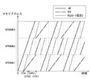
図3は、R2の処理レートが固定されていると仮定した場合に、W、R1、R2が処理対象とするVRAMが時間軸に沿って遷移していく様子を示した図である。ただし、ここではVRAM部111が3つのVRAM領域から成るものとし、図中のブロックがVRAM領域を示し、ブロック内の数字がVRAM番号である。
FIG. 3 is a diagram showing how the VRAMs to be processed by W, R1, and R2 transition along the time axis when it is assumed that the processing rate of R2 is fixed. However, here, it is assumed that the
図4は、図3に示す3つのVRAM領域におけるW、R1、R2の処理状況を示すグラフである。横軸は時間、縦軸は各VRAM領域のメモリアドレスである。 FIG. 4 is a graph showing the processing status of W, R1, and R2 in the three VRAM areas shown in FIG. The horizontal axis is time, and the vertical axis is the memory address of each VRAM area.
図5は、R2の処理レートが変動した場合におけるW、R1、R2の処理状況を示すグラフである。横軸は時間、縦軸は各VRAM領域のメモリアドレスである。なお、図5に示す例では、VRAM部111が最初は3つのVRAM領域で構成されているが、その後に新たにVRAM番号4のVRAM領域が追加される場合を示す。
FIG. 5 is a graph showing the processing status of W, R1, and R2 when the processing rate of R2 varies. The horizontal axis is time, and the vertical axis is the memory address of each VRAM area. In the example shown in FIG. 5, the
なお、図3〜図5は書き込みと読出しのフレームレートをそれぞれ、Wは80fps、R1は30fps、R2は100fpsとした場合の一例を図示したものである。 3 to 5 show an example in which the writing and reading frame rates are 80 fps, R1 is 30 fps, and R2 is 100 fps, respectively.
本実施の形態では、図6〜図9を参照して後述するVRAM書込読出処理により、図4及び図5に示すように、W(書き込み)を表す実線と、R1、R2(読出し)を表す2つの破線とが交差しないように制御される。これにより、VRAM領域へ画像信号を書込み中に更新途中の画像信号が読み出されることや、VRAM領域から画像信号を読み出し中に画像信号が更新されてしまうことがなくなるので、「胴切り」が発生しない。「胴切り」とは、前述したように、VRAM領域へ画像信号を書込み中に読み出しが追い越す、もしくは、VRAM領域から画像信号を読出し中に書き込みが追い越すことにより、画面の上部と下部で撮影された時刻が異なる画像が読み出される現象をいう。 In the present embodiment, as shown in FIGS. 4 and 5, a solid line representing W (write) and R1 and R2 (read) are obtained by VRAM write / read processing described later with reference to FIGS. Control is performed so that the two broken lines shown do not intersect. As a result, the image signal being updated is not read while the image signal is being written to the VRAM area, and the image signal is not updated while the image signal is being read from the VRAM area. . As described above, the “body cut” was taken at the top and bottom of the screen by reading overtaking while writing image signals to the VRAM area, or by overwriting writing while reading image signals from the VRAM area. A phenomenon in which images with different times are read out.
図6は、映像信号処理装置100で実行されるVRAM書込読出処理のうちの初期化処理の手順を示すフローチャートである。なお、このVRAM書込読出処理は、システム制御部108において、ROMに格納された制御プログラムをCPUが実行することによって行われる処理である。以下、このフローチャートに沿って説明する。
FIG. 6 is a flowchart showing the procedure of the initialization process in the VRAM writing / reading process executed by the video
システム制御部108が、VRAM管理情報部112の書込みVRAM番号記録部166に記録するVRAM番号(Wの書込み対象VRAMの番号)と、R1及びR2の読出し対象VRAM領域のVRAM番号とを1に設定する(S302)。
The
つぎに、メモリリード1フラグ領域162にVRAM番号1に対応するフラグを立て、メモリライトフラグ領域161と書込み順キュー領域164とをクリアする(S303)。
Next, a flag corresponding to VRAM
また、映像信号処理装置100が、画像表示部104での画像の表示と、圧縮回路107を通して記憶媒体106への圧縮画像の保存との両方を行う場合は、マスク領域167におけるすべてのVRAM領域に対応するフラグに1をセットし、一方、画像表示部104での画像の表示のみを行う場合は、マスク領域167におけるすべてのVRAM領域に対応するフラグに0をセットする(S304)。
In addition, when the video
続けて、W、R1、R2それぞれでの書込読出処理を開始する(S305)。 Subsequently, the writing / reading process in each of W, R1, and R2 is started (S305).
図7は、映像信号処理装置100で実行されるVRAM書込読出処理のうちのW(信号処理部109から出力された画像信号のVRAM部111への書込み)処理の手順を示すフローチャートである。
FIG. 7 is a flowchart illustrating a procedure of W (writing of an image signal output from the
VRAM管理情報部112の書込みVRAM番号記録部166に記録されているVRAM番号に対応するVRAM領域に画像信号を書込む(S311)。この書込みが完了した時点でメモリライトフラグ領域161に、書込み完了したVRAM領域に対応するフラグを立てる(S312)とともに、書込み完了VRAM番号記録部165に、書き込みが完了したVRAM領域のVRAM番号を記録し(S313)、さらに、書込み順キュー領域164の最後尾にこのVRAM番号を記録する(S314)。
The image signal is written in the VRAM area corresponding to the VRAM number recorded in the write VRAM
次に、VRAM部111に、書込み可能なVRAM領域が存在するか否かを判別する(S315)。すなわち、対応するVRAM領域どうしにおいて、メモリライトフラグ領域161に記録されたフラグとマスク領域167に記録されたフラグとの論理積を取ったものと、メモリリード1フラグ領域162に記録されたフラグの論理和をとり、それがゼロになるVRAM領域が存在するか否かを判別する。ゼロになるVRAM領域が存在するならばステップS316へ進み、ゼロになるVRAM領域が存在しなければステップS317へ進む。
Next, it is determined whether there is a writable VRAM area in the VRAM unit 111 (S315). That is, in the corresponding VRAM areas, the logical product of the flag recorded in the memory
ステップS316では、書込み可能なVRAM領域が複数あった場合、その中から1つのVRAM領域を選択する。例えば、該当する複数のVRAM領域のうちでVRAM番号が最も小さいVRAMを選択する。そしてステップS311へ戻る。 In step S316, if there are a plurality of writable VRAM areas, one VRAM area is selected from them. For example, the VRAM having the smallest VRAM number is selected from the corresponding plurality of VRAM areas. Then, the process returns to step S311.
ステップS317では、書込み可能なVRAM領域が存在しないので、VRAM部111に新しいVRAM領域を確保し、次のステップS318で、そのVRAM領域を次に書込みを行うべきVRAM領域として、そのVRAM番号を書込みVRAM番号記録部166に記録する。
In step S317, since there is no writable VRAM area, a new VRAM area is secured in the
図8は、映像信号処理装置100で実行されるVRAM書込読出処理のうちのR1(VRAM部111から画像表示処理回路105への画像信号の読み出し)処理の手順を示すフローチャートである。
FIG. 8 is a flowchart showing a procedure of R1 (reading of an image signal from the
まず、書込み完了VRAM番号記録部165にVRAM番号が記録されるまで読出しを開始せずに待機する(S320)。書込み完了VRAM番号記録部165にVRAM番号が記録されたらステップS321へ進んで、その記録されたVRAM番号のVRAM領域から画像表示処理回路105へ画像信号の読み出しを始める。
First, it waits without starting reading until the VRAM number is recorded in the write completion VRAM number recording unit 165 (S320). When the VRAM number is recorded in the write completion VRAM
画像信号の読出しが完了したら、次に、メモリリード1フラグ領域162において、読出しを完了したVRAM領域に対応するフラグをクリアする(S322)。 When the reading of the image signal is completed, the flag corresponding to the VRAM area where the reading is completed is cleared in the memory read 1 flag area 162 (S322).
次に、書込み完了VRAM番号記録部165に記録されているVRAM番号のVRAM領域を、次に読出しを行うべきVRAM領域に設定し(S323)、メモリリード1フラグ領域162において、その設定されたVRAM領域に対応するフラグを立てる(S324)。その後、ステップS321へ戻り、再度読出しを始める。
Next, the VRAM area of the VRAM number recorded in the write completion VRAM
なお、R1がWより遅い場合はステップS323において、書込みVRAM番号記録部166に記録されているVRAM番号のVRAM領域を、次に読出しを行うべきVRAM領域に設定してもよい。またR1がWより速い場合においても、R1が書込みVRAM番号記録部166に記録されているVRAM番号のVRAM領域から読み出しを開始してもWに追いつかないならば、書込みVRAM番号記録部166に記録されたVRAM番号のVRAM領域を、次に読出しを行うべきVRAM領域に設定してもよい。
If R1 is slower than W, in step S323, the VRAM area of the VRAM number recorded in the write VRAM
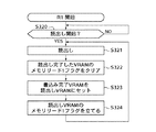
図9は、映像信号処理装置100で実行されるVRAM書込読出処理のうちのR2(VRAM部111から圧縮回路107への画像信号の読出し)処理の手順を示すフローチャートである。
FIG. 9 is a flowchart showing a procedure of R2 (reading of an image signal from the
書込み順キュー領域164に、書き込み完了したVRAM領域の番号が記録されるまで待ち(S330)、VRAM番号が記録されるとステップS331へ進んで、書込み順キュー領域164の先頭位置に記載されるVRAM番号のVRAM領域より画像信号の読み出しを始める。この読出しを完了したら、メモリライトフラグ領域161において、読出し完了したVRAM領域に対応するフラグをクリアする(S333)。
Wait until the number of the VRAM area that has been written is recorded in the write order queue area 164 (S330). When the VRAM number is recorded, the process proceeds to step S331, and the VRAM described at the head position of the write
次に、書込み順キュー領域164の記載が空であるか否かを調べ(S334)、空ならば読み出す画像信号が存在しないので、読出しを始めずに、書込み順キュー領域164にVRAM番号が記録されるまでポーリングしながら待機する(S334でYES)。
Next, it is checked whether or not the description of the write
書込み順キュー領域164が空でないときは、ステップS335へ進んで、ステップS331で行った読出しの完了時刻(画像信号の圧縮処理に時間がかかると遅くなる)が、1フレーム先のWの書込み完了時刻より遅いか否かを判別する。遅い場合はR2の読出し完了時において圧縮処理すべき記憶領域が更に1つ残っている状態なので、圧縮処理を急ぐためにステップS338へ進む。また、遅くない場合はステップS336へ進む。
When the writing
ステップS338では、圧縮回路107での量子化テーブルの値を変更(圧縮率を変更)して圧縮率を上げたり、圧縮回路107へ供給されるクロック信号の周波数を上げたりして、圧縮速度を速くする。
In step S338, the value of the quantization table in the
ステップS336では、書込み順キュー領域164の先頭位置に記載されたVRAM番号を取り出して、このVRAM番号のVRAM領域を、R2の次の読出しVRAM領域に設定する。そしてステップS331へ戻る。
In step S336, the VRAM number described at the head position of the write
次に、図4および図5に示すW,R1及びR2の処理状況の一例を参照して、上記のVRAM書込読出処理を具体的に説明する。 Next, the VRAM writing / reading process will be described in detail with reference to an example of the processing status of W, R1, and R2 shown in FIGS.
まず、R2の圧縮速度が変化しない場合におけるW,R1及びR2の処理状況の一例を示す図4を参照して、時間軸に沿って説明する。 First, a description will be given along the time axis with reference to FIG. 4 showing an example of the processing status of W, R1, and R2 when the compression speed of R2 does not change.
初期化処理として、書込みVRAM番号記録部166にVRAM番号1を記録し、かつ、R1及びR2の読出し処理対象のVRAM領域のVRAM番号を1にする(S302)。さらにメモリリード1フラグ領域162においてVRAM番号1のVRAM領域に対応するフラグを立て(フラグに1をセット)、メモリライトフラグ領域161において全部のVRAM領域に対応するフラグをクリア(フラグに0をセット)し、書込み順キュー領域164のVRAM番号の記載をクリアする(S303)。また図4に示す例では、映像信号処理装置100が画像表示部104での画像の表示と、圧縮回路107を通して記憶媒体106への圧縮画像の保存との両方を行うので、マスク領域167におけるすべてのVRAM領域に対応するフラグに1をセットする(S304)。
As initialization processing,
図4に示す時刻0で、WはVRAM番号1のVRAM領域へ画像信号の書き込みを開始する(S311)。
At
時刻t1wで、WはVRAM番号1のVRAM領域への書き込みを完了し、この時点で、書込み完了VRAM番号記録部165にVRAM番号1が記録される(S313)とともに、書込み順キュー領域164にVRAM番号1が記録される(S314)。このとき、VRAM領域ごとに、メモリライトフラグ領域161に記載のフラグとマスク領域167に記載のフラグとの論理積を取ったものと、メモリリード1フラグ領域162との論理和を取ると(S315)、VRAM番号2とVRAM番号3とに対応するフラグがゼロになっているので、それらのうち番号の小さいVRAM番号2のVRAM領域を、Wの書込み対象として選択し、VRAM番号2を書込みVRAM番号記録部166に更新記録する(S316)。
At time t1w, W completes writing
時刻t1wで、ステップS313で書込み完了VRAM番号記録部165にVRAM番号1が記録されたので、R1は、VRAM番号1のVRAM領域からの読出しを開始する(S321)。また、ステップS313で書込み順キュー領域164にVRAM番号1が記録されたので、R2は、書込み順キュー領域164に記録されたVRAM番号1のVRAM領域から読出しを開始する(S330及びS331)。なお、この読出し開始に伴い、書込み順キュー領域164の記載内容はクリアされる。
At time t1w, since
時刻t1R2で、R2は、VRAM番号1のVRAM領域からの読出しを完了する。このとき、書込み順キュー領域164は空なので、R2は時刻t2R2まで待機する。
At time t1R2, R2 completes reading from the VRAM area of
時刻t1R1で、R1は、VRAM番号1のVRAM領域からの読出しを完了するので、メモリリード1フラグ領域162においてVRAM番号1に対応するフラグをクリアする(S322)。この時点で、書込み完了VRAM番号記録部165にはVRAM番号3が記録されているが、このVRAM番号3を、R1が次に読出し処理するべきVRAM領域の番号に設定して(S323)、さらにメモリリード1フラグ領域162においてVRAM番号3に対応するフラグを立て(S324)、読出しを続ける。
At time t1R1, R1 completes reading from the
以降、図6〜図9に示す各フローチャートに従ってVRAM書込読出処理を進めていくと、図4に示すような動作になる。 Thereafter, when the VRAM writing / reading process proceeds according to the flowcharts shown in FIGS. 6 to 9, the operation shown in FIG. 4 is performed.
次に、R2の圧縮速度が変化する場合におけるW,R1及びR2の処理状況の一例を示す図5を参照して、時間軸に沿って説明する。 Next, a description will be given along the time axis with reference to FIG. 5 showing an example of the processing status of W, R1, and R2 when the compression speed of R2 changes.
図5に示す時刻t1R2では、R2は、VRAM番号1のVRAM領域から読出しを始めるが(S331)、このフレームの圧縮に時間がかかり、時刻t2R2になってようやく完了したとする。 At time t1R2 shown in FIG. 5, it is assumed that R2 starts reading from the VRAM area of VRAM number 1 (S331), but it takes time to compress this frame, and it is finally completed at time t2R2.
時刻t1wで、WはVRAM番号3のVRAM領域への書き込みが完了するので、VRAM領域ごとに、メモリライトフラグ領域161に記載のフラグとマスク領域167に記載のフラグとの論理積と、メモリリード1フラグ領域162に記載のフラグの論理和とを取ると、VRAM番号1、2、3に対応するフラグが共に1であるので、新たにVRAM番号4を確保し(S317)、書込みVRAM番号記録部166にVRAM番号4を記録する(S318)。
At time t1w, W completes writing to the VRAM area with
以降、図6〜図9に示す各フローチャートに従ってVRAM書込読出処理を進めていくと、図5に示すような動作になる。 Thereafter, when the VRAM writing / reading process proceeds according to the flowcharts shown in FIGS. 6 to 9, the operation shown in FIG. 5 is performed.
上記説明では、映像信号処理装置100が、画像表示部104での画像の表示と、圧縮回路107を通して記憶媒体106への圧縮画像の保存とを並列して行うことを前提としているが、画像表示部104で画像の表示だけを行うときは、図6のステップS304において、マスク領域167に記載の全部のVRAM領域に対応するフラグをすべて0にセットしてから、図7〜図9に示す各フローチャートに沿って処理を行うようにすればよい。また、画像表示部104での画像の表示と、圧縮回路107を通して記憶媒体106への圧縮画像の保存とを並列して行っていた状態から、画像表示部104での画像の表示だけを行う状態に遷移するには、メモリライトフラグ領域161に記載の全部のVRAM領域に対応するフラグをすべてクリアした後で、図6に示す初期化処理から処理を始めるようにすればよい。
In the above description, it is assumed that the video
また、上記説明では、VRAM部111内のVRAM領域の数が可変であることを前提にしていたが、VRAM領域の数が固定の場合は、圧縮処理に時間がかかった場合に相当するので、図9のステップS335及びステップS338に従い、圧縮速度を上げて圧縮処理にかかる時間を低減させるようにすれば、書込み順キュー領域164が、圧縮処理待ちの画像信号に対応するVRAM番号で一杯になることを防ぐことができる。
In the above description, it is assumed that the number of VRAM areas in the
〔第2の実施の形態〕
次に、本発明の第2の実施の形態を説明する。
[Second Embodiment]
Next, a second embodiment of the present invention will be described.
第2の実施の形態の構成は、基本的に第1の実施の形態の構成と同じであるので、第2の実施の形態の説明においては、第1の実施の形態の構成と同一部分には同一の参照符号を付して、第1の実施の形態の説明を流用し、異なる部分だけを説明する。 Since the configuration of the second embodiment is basically the same as the configuration of the first embodiment, in the description of the second embodiment, the same parts as the configuration of the first embodiment are used. Are denoted by the same reference numerals, and the description of the first embodiment is used, and only different portions will be described.
第2の実施の形態では、図1に示す第1の実施の形態におけるメモリ部113、VRAM部111及びVRAM管理情報部112に代わって、メモリ部113a、VRAM部111a及びVRAM管理情報部112aを設ける。VRAM部111aは、予め定められた数のVRAM領域を備え、その数は増減することはない。
In the second embodiment, the memory unit 113a, the VRAM unit 111a, and the VRAM
図10は、第2の実施の形態におけるVRAM管理情報部112aの内部メモリ構成を示す図である。
FIG. 10 is a diagram illustrating an internal memory configuration of the VRAM
すなわち、VRAM管理情報部112aは、メモリライトフラグ領域141と、書込み完了VRAM番号記録部142と、空きVRAM数記録部143とから構成される。
That is, the VRAM
メモリライトフラグ領域141には、第1の実施の形態におけるメモリライトフラグ領域161と同様に、VRAM部111aの複数のVRAM領域にそれぞれ対応した複数のフラグが格納され、それらのフラグは、画像信号の対応VRAM領域への書き込みが完了したときに立てられ(1に設定)、対応VRAM領域から圧縮回路107への画像信号の読出しが完了したときにクリアされる(0に設定)。
Similar to the memory
書込み完了VRAM番号記録部142には、最後に書き込みの完了したVRAM領域の番号が記録される。
The write completion VRAM
空きVRAM数記録部143は、現在の空きVRAM領域の数を記録しており、1つのVRAM領域への書き込みが完了するごとにデクリメントされ、また1つのVRAM領域から圧縮回路107への読出しが完了するごとにインクリメントされる。
The free VRAM
図11は、第2の実施の形態において、W、R1、R2が処理対象とするVRAM領域が時間軸に沿って遷移していく様子を示した図である。ただし、ここではVRAM部111aが4個のVRAM領域から成るものとし、図中のブロックがVRAM領域を示し、ブロック内の数字がVRAM番号である。 FIG. 11 is a diagram showing how the VRAM areas targeted by W, R1, and R2 transition along the time axis in the second embodiment. However, here, it is assumed that the VRAM unit 111a is composed of four VRAM areas, the block in the figure indicates the VRAM area, and the number in the block is the VRAM number.
図12は、図11に示す4個のVRAM領域におけるW、R1、R2の処理状況を示すグラフである。横軸は時間、縦軸は各VRAM領域のメモリアドレスである。 FIG. 12 is a graph showing the processing status of W, R1, and R2 in the four VRAM areas shown in FIG. The horizontal axis is time, and the vertical axis is the memory address of each VRAM area.
なお、図11及び図12における書き込みと読出しのフレームレートは、Wを80fps、R1を30fps、R2を100fpsとする。 11 and 12, the writing and reading frame rates are 80 fps for W, 30 fps for R1, and 100 fps for R2.
第2の実施の形態では、図13〜図16を参照して後述するVRAM書込読出処理により、図12に示すように、W(書き込み)を表す実線と、R1、R2(読出し)を表す2つの破線とが交差しないように制御される。これにより、VRAM領域へ画像信号を書込み中に更新途中の画像信号が読み出されることや、VRAM領域から画像信号を読み出し中に画像信号が更新されてしまうことがなくなるので、前述の「胴切り」が発生しない。 In the second embodiment, a VRAM write / read process described later with reference to FIGS. 13 to 16 represents a solid line representing W (write) and R1 and R2 (read) as shown in FIG. Control is performed so that the two broken lines do not intersect. As a result, the image signal being updated is not read while the image signal is being written to the VRAM area, and the image signal is not updated while the image signal is being read from the VRAM area. Does not occur.
図13は、第2の実施の形態における映像信号処理装置100で実行されるVRAM書込読出処理のうちの初期化処理の手順を示すフローチャートである。
FIG. 13 is a flowchart showing a procedure of an initialization process in the VRAM writing / reading process executed by the video
先ず、システム制御部108がVRAM部111a内のVRAM領域の数を空きVRAM数記録部143に記録する(S201)。また、メモリライトフラグ領域141において、VRAM部111aの4つのVRAM領域に対応する4つのフラグをクリア(0に設定)する(S202)。
First, the
続けて、W、R1、R2それぞれでの書込読出処理を開始する(S203)。 Subsequently, the writing / reading process in each of W, R1, and R2 is started (S203).
図14は、第2の実施の形態における映像信号処理装置100で実行されるVRAM書込読出処理のうちのW(信号処理部109から出力された画像信号のVRAM部111aへの書込み)処理の手順を示すフローチャートである。
FIG. 14 shows the W (writing of the image signal output from the
設定されたVRAM領域(この処理の始めて行う場合は、VRAM番号1に対応するVRAM領域)に画像信号を書込む(S211)。この書込みが完了した時点で、メモリライトフラグ領域141において、書き込みが完了したVRAM領域に対応するフラグを立てる(1にセット)とともに(S212)、書き込みが完了したVRAM領域のVRAM番号を書込み完了VRAM番号記録部142に記録する(S213)。この書き込みによって空きVRAM領域の数が一つ減るので、空きVRAM数記録部143でデクリメントを行う(S214)。
The image signal is written in the set VRAM area (in the case of performing this process for the first time, the VRAM area corresponding to VRAM number 1) (S211). When this writing is completed, a flag corresponding to the VRAM area for which writing has been completed is set (set to 1) in the memory write flag area 141 (S212), and the VRAM number of the VRAM area for which writing has been completed is set to the write completion VRAM. It records in the number recording part 142 (S213). Since this writing reduces the number of free VRAM areas by 1, the free VRAM
書込み完了VRAM番号記録部142に記録されたVRAM番号が、終端のVRAM番号(4)と一致するか否かを判別し(S215)、一致するならばステップS217へ進み、一致しないならばステップS216へ進む。
It is determined whether or not the VRAM number recorded in the write completion VRAM
ステップS217では、先頭の番号(1)のVRAM領域を、次に書込み処理を行うべきVRAM領域に設定し、ステップS211へ戻る。 In step S217, the VRAM area with the top number (1) is set as the VRAM area to be subjected to the next writing process, and the process returns to step S211.
ステップS216では、書き込みの完了したVRAM領域の番号をインクリメントした番号をもつVRAM領域を、次に書込み処理を行うべきVRAM領域に設定し、ステップS211へ戻る。 In step S216, the VRAM area having a number obtained by incrementing the number of the VRAM area in which writing has been completed is set as the VRAM area to be subjected to the next writing process, and the process returns to step S211.
図15は、第2の実施の形態における映像信号処理装置100で実行されるVRAM書込読出処理のうちのR1(VRAM部111aから画像表示処理回路105への画像信号の読み出し)処理の手順を示すフローチャートである。
FIG. 15 illustrates a procedure of R1 (reading of an image signal from the VRAM unit 111a to the image display processing circuit 105) in the VRAM writing / reading process executed by the video
まず、書込み完了VRAM番号記録部142にVRAM番号が記録されるまで読出しを開始せずに待機する(S220)。書込み完了VRAM番号記録部142にVRAM番号が記録されたら、先頭のVRAM番号をもつVRAM領域より画像信号を読み出す(S221)。この読出しを完了したら、書込み完了VRAM番号記録部142に記録されているVRAM番号をもつVRAM領域を、次の読出し処理対象にする(S222)。
First, it waits without starting reading until the VRAM number is recorded in the write completion VRAM number recording unit 142 (S220). When the VRAM number is recorded in the write completion VRAM
図16は、第2の実施の形態における映像信号処理装置100で実行されるVRAM書込読出処理のうちのR2(VRAM部111aから圧縮回路107への画像信号の読出し)処理の手順を示すフローチャートである。
FIG. 16 is a flowchart showing a procedure of R2 (reading of an image signal from the VRAM unit 111a to the compression circuit 107) in the VRAM writing / reading process executed by the video
Wの書込みVRAM領域とR2の読出しVRAM領域とが一致しなくなるまで待ってから(S230)、ステップS231へ進み、書込み完了VRAM番号記録部142に記録されているVRAM番号のVRAM領域から画像信号を読み出して圧縮する。読出しが完了したら、メモリライトフラグ領域141において、読出しを完了したVRAM領域の番号に対応するフラグをクリアする(S232)とともに、空きVRAM数記憶部143に記載のVRAM領域の数をインクレメントする(S233)。
After waiting until the write VRAM area of W and the read VRAM area of R2 do not match (S230), the process proceeds to step S231, and the image signal is received from the VRAM area of the VRAM number recorded in the write completion VRAM
次に、書込み完了VRAM番号記録部142に記載されたVRAM番号と終端のVRAM番号(4)とが一致するか否かを判別する(S234)。一致する場合はステップS236へ進み、一致しない場合はステップS235へ進む。
Next, it is determined whether or not the VRAM number written in the write completion VRAM
ステップS236では、先頭の番号(1)のVRAM領域を、次に読出し処理を行うべきVRAM領域に設定し、ステップS237へ進む。 In step S236, the VRAM area with the head number (1) is set as the VRAM area to be read next, and the process proceeds to step S237.
ステップS235では、書き込みの完了したVRAM領域の番号をインクリメントした番号をもつVRAM領域を、次に読出し処理を行うべきVRAM領域に設定し、ステップS237へ進む。 In step S235, the VRAM area having a number obtained by incrementing the number of the VRAM area in which writing has been completed is set as the VRAM area to be read next, and the process proceeds to step S237.
ステップS237では、ステップS235またはステップS236で設定された次に書込み処理を行うべきVRAM領域に対してWによる書き込みが完了するまで待機する。この書き込みが完了すると、ステップS238へ進む。 In step S237, the process waits until the writing by W is completed for the VRAM area to be subjected to the next writing process set in step S235 or step S236. When this writing is completed, the process proceeds to step S238.
ステップS238では、空きVRAM数記録部143に記載されていつ空きVRAM領域数が所定の閾値より少ないか否かを判別し、少ないならばステップS239へ進み、少なくないならばステップS239をスキップしてステップS231へ戻る。
In step S238, it is determined whether or not the number of free VRAM areas described in the free VRAM
ステップS239では、圧縮回路107での量子化テーブルの値を変更(圧縮率を変更)して圧縮率を上げたり、圧縮回路107へ供給されるクロック信号の周波数を上げたりして、圧縮速度を速くし、これによって、圧縮回路107への読出しが行われていないVRAM領域の数を減らして、空きVRAM領域の数を多く確保するようにする。なお、圧縮速度を上げた結果、再度のステップS238の実行時に、空きVRAM領域数が所定の閾値以上になっていた場合には、量子化テーブルの値と圧縮回路107に供給するクロックスピードとを元に戻して圧縮速度を遅くするようにする。
In step S239, the compression rate is increased by changing the value of the quantization table in the compression circuit 107 (changing the compression rate) to increase the compression rate, or increasing the frequency of the clock signal supplied to the
次に、図12に示すW,R1及びR2の処理状況の一例を参照して、上記のVRAM書込読出処理を,時間軸に沿って具体的に説明する。 Next, the VRAM writing / reading process described above will be specifically described along the time axis with reference to an example of the processing situation of W, R1, and R2 shown in FIG.
先ず初期化処理として、空きVRAM領域数記録部143に、VRAM部111a内のVRAM領域の数である4を記録する(S201)。また、メモリライトフラグ領域141をクリアする(S202)。
First, as initialization processing, 4 which is the number of VRAM areas in the VRAM unit 111a is recorded in the free VRAM area number recording unit 143 (S201). Further, the memory
図12に示す時刻0において、WはVRAM番号1への書き込みを始める。
At
時刻t1wで、Wは、VRAM番号1のVRAM領域への書き込みを完了するので、メモリライトフラグ領域141において、VRAM番号1に対応するフラグを立てる(S212)。また、書込み完了VRAM番号記録部142にVRAM番号1を記録し(S213)、空きVRAM数記録部143に記録されている空きVRAM領域数を4から3に減らす(S214)。
At time t1w, W completes the writing of the
ここで、書込み完了VRAM番号記録部142に記録されているVRAM番号1と終端のVRAM領域のVRAM番号4とは一致しないので(S215でNO)、VRAM番号1をインクレメントして得られたVRAM番号2を、次に書込みが行われるべきVRAM領域のVRAM番号にする(S216)。
Here, since the
時刻t1wで書込み完了番号記録部142にVRAM番号1が記録されたので、R1は、このVRAM番号1をもつVRAM領域から読出しを始める(S220とS221)。
Since
さらに時刻t1wの時点でメモリライトフラグ領域141においてVRAM番号1に対応するフラグが立ったので(S230)、R2も、VRAM番号1のVRAM領域から読出しを始める(S231)。
Furthermore, since a flag corresponding to VRAM
時刻t1R2で、R2はVRAM番号1のVRAM領域からの読出しを完了するので、メモリライトフラグ領域141においてVRAM番号1に対応するフラグをクリアし(S232)、空きVRAM領域数記録部143に記録されている空きVRAM領域数を3から4に増やす(S233)。このとき、書込み完了VRAM番号記録部142に記録されているVRAM番号1と終端のVRAM領域のVRAM番号4とは一致しないので(S234でNO)、VRAM番号1をインクレメントして得られたVRAM番号2を、次に書込みを行うべきVRAM領域の番号にする(S235)。
At time t1R2, R2 completes reading from the VRAM area of
ところで、時刻t1R2の時点ではメモリライトフラグ領域141においてVRAM番号2に対応するフラグがまだ立っていないので、時刻t2R2でWによるVRAM番号2のVRAM領域への書き込みが完了して、メモリライトフラグ領域141においてVRAM番号2に対応するフラグが立てられるまで待機する(S237)。
By the way, since the flag corresponding to VRAM
時刻t1R1では、R1が、VRAM番号1のVRAM領域からの読出しを完了する。この時点で書込み完了VRAM番号記録部142にはVRAM番号3が記録されているので、VRAM番号3のVRAM領域を、次に読出し処理を行うべきVRAM領域にする(S222)。
At time t1R1, R1 completes reading from the VRAM area with
時刻t2wでは、Wが、VRAM番号4のVRAM領域への書き込みを完了するので、メモリライトフラグ領域141においてVRAM番号4に対応するフラグを立て(S212)、書込み完了VRAM番号記録部142にVRAM番号4を記録し(S213)、空きVRAM領域数記録部143に記録した空きVRAM領域数を4から3に減らす(S214)。
At time t2w, W completes the writing of the
このとき、書込み完了VRAM番号記録部142に記録されているVRAM番号4と終端のVRAM領域のVRAM番号4とが一致するので(S215でYES)、先頭のVRAM番号1のVRAM領域を、次に書込みを行うべきVRAM領域の番号に設定して(S217)、書き込みを続ける。
At this time, the
以降、図13〜図16に示す各フローチャートに従ってVRAM書込読出処理を進めていくと、図12に示すような動作になる。 Thereafter, when the VRAM writing / reading process proceeds according to the flowcharts shown in FIGS. 13 to 16, the operation shown in FIG. 12 is performed.
〔他の実施の形態〕
なお、本発明の目的は、前述した各実施の形態の機能を実現するソフトウェアのプログラムコードを記録した記憶媒体を、システムまたは装置に供給し、そのシステムまたは装置のコンピュータ(またはCPU、MPU等)が記憶媒体に格納されたプログラムコードを読み出して実行することによっても達成される。
[Other Embodiments]
The object of the present invention is to supply a storage medium storing software program codes for realizing the functions of the above-described embodiments to a system or apparatus, and a computer (or CPU, MPU, etc.) of the system or apparatus. Is also achieved by reading and executing the program code stored in the storage medium.
この場合、記憶媒体から読み出されたプログラムコード自体が本発明の新規な機能を実現することになり、そのプログラムコードを記憶した記憶媒体およびプログラムは本発明を構成することになる。 In this case, the program code itself read from the storage medium realizes the novel function of the present invention, and the storage medium and program storing the program code constitute the present invention.
また、プログラムコードを供給するための記憶媒体としては、例えば、フレキシブルディスク、ハードディスク、光ディスク、光磁気ディスク、CD−ROM、CD−R、CD−RW、DVD−ROM、DVD−RAM、DVD−RW、DVD+RW、磁気テープ、不揮発性のメモリカード、ROM等を用いることができる。或いは、上記プログラムは、インターネット、商用ネットワーク、若しくはローカルエリアネットワーク等に接続される他のコンピュータやデータベース等からダウンロードすることにより供給される。 The storage medium for supplying the program code is, for example, a flexible disk, hard disk, optical disk, magneto-optical disk, CD-ROM, CD-R, CD-RW, DVD-ROM, DVD-RAM, DVD-RW. DVD + RW, magnetic tape, nonvolatile memory card, ROM, etc. can be used. Alternatively, the program is supplied by downloading from another computer or database connected to the Internet, a commercial network, a local area network, or the like.
また、コンピュータが読み出したプログラムコードを実行することにより、前述した各実施の形態の機能が実現されるだけでなく、そのプログラムコードの指示に基づき、コンピュータ上で稼動しているOS(オペレーティングシステム)等が実際の処理の一部または全部を行い、その処理によって前述した各実施の形態の機能が実現される場合も含まれる。 Further, by executing the program code read by the computer, not only the functions of the above-described embodiments are realized, but also an OS (Operating System) running on the computer based on the instruction of the program code. Includes a case where the functions of the above-described embodiments are realized by performing part or all of the actual processing.
更に、記憶媒体から読み出されたプログラムコードが、コンピュータに挿入された機能拡張ボードやコンピュータに接続された機能拡張ユニットに備わるメモリに書き込まれた後、そのプログラムコードの指示に基づき、その機能拡張ボードや機能拡張ユニットに備わるCPU等が実際の処理の一部または全部を行い、その処理によって前述した各実施の形態の機能が実現される場合も含まれる。 Further, after the program code read from the storage medium is written in a memory provided in a function expansion board inserted into the computer or a function expansion unit connected to the computer, the function expansion is performed based on the instruction of the program code. This includes the case where the CPU or the like provided in the board or the function expansion unit performs part or all of the actual processing, and the functions of the above-described embodiments are realized by the processing.
100 映像信号処理装置
101 撮像レンズ
102 撮像素子
103 A/D変換器
104 画像表示部
105 画像表示処理回路
106 記憶媒体
107 圧縮回路
108 システム制御部(メモリ制御手段)
109 信号処理部
110 メモリ制御部(メモリ制御手段、制御手段)
111 VRAM部
112 VRAM管理情報部
113 メモリ部
161 メモリライトフラグ領域
162 メモリリード1フラグ領域
164 書込み順キュー領域
165 書込み完了VRAM番号記録部
166 書込みVRAM番号記録部
167 マスク領域
DESCRIPTION OF
109
111
Claims (14)
前記撮像素子から出力された画像信号に対して信号処理を施す信号処理部と、
前記信号処理部から出力される画像信号を記憶するVRAM(Video Random Access Memory)部であって、それぞれが1フレームの画像信号を記憶する3つ以上の記憶領域からなるVRAM部と、
前記VRAM部の各記憶領域に関して、画像信号の書き込みが完了した記憶領域、及び画像信号の書き込みが完了した順番を示す管理情報を保持するVRAM管理情報記憶部と、
前記VRAM管理情報記憶部の保持する管理情報に基づき、前記VRAM部から前記3つ以上の記憶領域にそれぞれ記憶される画像信号を書き込みが完了した順に第1の読出し速度で読み出して、当該読み出された画像信号に対して圧縮処理を施す画像圧縮部と、
前記VRAM管理情報記憶部の保持する管理情報に基づき、前記VRAM部から前記3つ以上の記憶領域のうち最後に書き込みが完了した記憶領域に記憶される画像信号を第2の読出し速度で読み出して、当該読み出された画像信号に対して画像表示処理を施す画像表示処理部と、
前記画像表示処理部から出力された画像信号に基づき画像表示を行う画像表示部と、
前記画像圧縮部による画像信号の読み出しが完了していない記憶領域、及び前記画像表示処理部による画像信号の読み出しを行っている記憶領域を検出し、当該検出の結果に基づいて前記信号処理部から出力される画像信号の書き込まれる記憶領域を前記3つ以上の記憶領域の中から選択することによって、前記VRAM部の各記憶領域における書き込みアドレス及び読み出しアドレスの一方が他方を追い越すことのないよう制御するメモリ制御部と、
を有することを特徴とする映像信号処理装置。 A video signal processing apparatus including an image sensor that outputs an image signal corresponding to a subject image,
A signal processing unit that performs signal processing on the image signal output from the imaging element;
A VRAM (Video Random Access Memory) section for storing an image signal output from the signal processing unit, and the VRA M portions, each consisting of three or more storage areas for storing image signals of one frame,
For each storage area of the VRAM unit, a VRAM management information storage unit that holds management information indicating a storage area in which image signal writing has been completed, and an order in which image signal writing has been completed ;
Based on said management information held by the VRAM management information storage unit, the reading from the VRAM unit at a first reading speed in order to write an image signal has been completed stored respectively into the three or more storage areas, leaving the reading An image compression unit that performs compression processing on the image signal that has been processed;
Based on said management information held by the VRAM management information storage unit, the image signals last stored in the storage area writing has been completed among said from the VRAM 3 or more storage area is read out at a second readout speed An image display processing unit that performs image display processing on the read image signal;
An image display unit for displaying an image based on the image signal output from the image display processing unit;
A storage area where the image signal reading by the image compression unit is not completed and a storage area where the image display processing unit reads the image signal are detected, and the signal processing unit detects from the detection result based on the detection result. By selecting a storage area to which the output image signal is written from among the three or more storage areas, control is performed so that one of the write address and the read address in each storage area of the VRAM section does not overtake the other. A memory control unit ,
A video signal processing apparatus comprising:
前記メモリ制御部は、前記信号処理部から出力される画像信号を前記VRAM部の1つの記憶領域へ書込み完了したあと、該書込み完了した記憶領域の番号が前記一連の番号の終端の番号である場合は、前記一連の番号の先頭の番号を付された記憶領域を、次に書き込むべき記憶領域とし、一方、前記書込み完了した記憶領域の番号が前記一連の番号の終端の番号ではない場合は、該書込み完了した記憶領域の番号をインクリメントして得られた番号をもつ記憶領域を、次に書き込むべき記憶領域とすることを特徴とする請求項1に記載の映像信号処理装置。 Each storage area of the VRAM unit is given a series of numbers,
The memory control unit completes the writing of the image signal output from the signal processing unit to one storage area of the VRAM unit, and then the number of the storage area that has been written is the end number of the series of numbers. If the storage area numbered at the beginning of the series number is the storage area to be written next, while the number of the storage area that has been written is not the terminal number of the series number 2. The video signal processing apparatus according to claim 1, wherein a storage area having a number obtained by incrementing the number of the storage area that has been written is set as a storage area to be written next.
前記VRAM部の各記憶領域に関して、画像信号の書き込みが完了した記憶領域、及び画像信号の書き込みが完了した順番を示す管理情報を記憶装置に保持する保持ステップと、
前記画像圧縮部による画像信号の読み出しが完了していない記憶領域、及び前記画像表示処理部による画像信号の読み出しを行っている記憶領域を検出し、当該検出の結果に基づいて前記信号処理部から出力される画像信号の書き込まれる記憶領域を前記3つ以上の記憶領域の中から選択することによって、前記VRAM部の各記憶領域における書き込みアドレス及び読み出しアドレスの一方が他方を追い越すことのないよう制御するメモリ制御ステップと、
を有することを特徴とするメモリ制御方法。 Stores an imaging device that outputs an image signal corresponding to the subject image, a signal processing unit which performs signal processing on the image signal output from this image pickup device, an image signal output from this signal processing unit a VRAM (Video Random Access memory) unit, and the VRA M portions, each consisting of three or more storage areas for storing image signals of one frame, based on the management information held by the person the VRAM management information storage unit, An image compression unit that reads image signals stored in the three or more storage areas from the VRAM unit at a first reading speed in the order of completion of writing, and performs compression processing on the read image signals. When the last write of those the basis of the management information held in the VRAM management information storage unit, the three or more storage areas from the VRAM unit Is applied to a video signal processing apparatus including an image display processing unit that reads an image signal stored in a storage area in which image processing is completed at a second readout speed and performs image display processing on the read image signal Memory control method, comprising:
For each storage area of the VRAM unit, a holding step for holding in the storage device management information indicating a storage area in which image signal writing has been completed and an order in which image signal writing has been completed ;
A storage area in which reading of the image signal by the image compression unit is not completed and a storage area in which the image signal is read by the image display processing unit are detected, and based on the detection result, the signal processing unit By selecting a storage area to which the output image signal is written from among the three or more storage areas, control is performed so that one of the write address and the read address in each storage area of the VRAM section does not overtake the other. A memory control step to
A memory control method comprising:
前記VRAM部の各記憶領域に関して、画像信号の書き込みが完了した記憶領域、及び画像信号の書き込みが完了した順番を示す管理情報を記憶装置に保持する保持ステップと、
前記画像圧縮部による画像信号の読み出しが完了していない記憶領域、及び前記画像表示処理部による画像信号の読み出しを行っている記憶領域を検出し、当該検出の結果に基づいて前記信号処理部から出力される画像信号の書き込まれる記憶領域を前記3つ以上の記憶領域の中から選択することによって、前記VRAM部の各記憶領域における書き込みアドレス及び読み出しアドレスの一方が他方を追い越すことのないよう制御するメモリ制御ステップと、
をコンピュータに実行させることを特徴とするプログラム。 Storing an imaging device that outputs an image signal corresponding to the subject image, a signal processing unit which performs signal processing on the image signal output from this image pickup device, an image signal output from this signal processing unit a VRAM (Video Random Access memory) unit, and the VRA M portions, each consisting of three or more storage areas for storing image signals of one frame, based on the management information held by the person the VRAM management information storage unit, An image compression unit that reads image signals stored in the three or more storage areas from the VRAM unit at a first reading speed in the order of completion of writing, and performs compression processing on the read image signals. When the last write of those the basis of the management information held in the VRAM management information storage unit, the three or more storage areas from the VRAM unit Is applied to a video signal processing apparatus including an image display processing unit that reads an image signal stored in a storage area in which image processing is completed at a second readout speed and performs image display processing on the read image signal In a program for causing a computer to execute the memory control method to be executed,
For each storage area of the VRAM unit, a holding step for holding in the storage device management information indicating a storage area in which image signal writing has been completed and an order in which image signal writing has been completed ;
A storage area in which reading of the image signal by the image compression unit is not completed and a storage area in which the image signal is read by the image display processing unit are detected, and based on the detection result, the signal processing unit By selecting a storage area to which the output image signal is written from among the three or more storage areas, control is performed so that one of the write address and the read address in each storage area of the VRAM section does not overtake the other. A memory control step to
A program that causes a computer to execute.
Priority Applications (2)
| Application Number | Priority Date | Filing Date | Title |
|---|---|---|---|
| JP2004200766A JP4500610B2 (en) | 2004-07-07 | 2004-07-07 | Video signal processing apparatus, memory control method, and program |
| US11/176,865 US7796136B2 (en) | 2004-07-07 | 2005-07-07 | Image signal processing apparatus, memory control method, and program for implementing the method |
Applications Claiming Priority (1)
| Application Number | Priority Date | Filing Date | Title |
|---|---|---|---|
| JP2004200766A JP4500610B2 (en) | 2004-07-07 | 2004-07-07 | Video signal processing apparatus, memory control method, and program |
Publications (3)
| Publication Number | Publication Date |
|---|---|
| JP2006025124A JP2006025124A (en) | 2006-01-26 |
| JP2006025124A5 JP2006025124A5 (en) | 2007-08-23 |
| JP4500610B2 true JP4500610B2 (en) | 2010-07-14 |
Family
ID=35540856
Family Applications (1)
| Application Number | Title | Priority Date | Filing Date |
|---|---|---|---|
| JP2004200766A Expired - Fee Related JP4500610B2 (en) | 2004-07-07 | 2004-07-07 | Video signal processing apparatus, memory control method, and program |
Country Status (2)
| Country | Link |
|---|---|
| US (1) | US7796136B2 (en) |
| JP (1) | JP4500610B2 (en) |
Families Citing this family (8)
| Publication number | Priority date | Publication date | Assignee | Title |
|---|---|---|---|---|
| JP2007020112A (en) * | 2005-07-11 | 2007-01-25 | Canon Inc | Image signal processing apparatus, image signal processing method and imaging device |
| US10073939B2 (en) * | 2015-11-04 | 2018-09-11 | Chronos Tech Llc | System and method for application specific integrated circuit design |
| US11550982B2 (en) | 2015-11-04 | 2023-01-10 | Chronos Tech Llc | Application specific integrated circuit interconnect |
| US9977853B2 (en) | 2015-11-04 | 2018-05-22 | Chronos Tech Llc | Application specific integrated circuit link |
| US10181939B2 (en) | 2016-07-08 | 2019-01-15 | Chronos Tech Llc | Systems and methods for the design and implementation of an input and output ports for circuit design |
| US10889958B2 (en) * | 2017-06-06 | 2021-01-12 | Caterpillar Inc. | Display system for machine |
| US10637592B2 (en) | 2017-08-04 | 2020-04-28 | Chronos Tech Llc | System and methods for measuring performance of an application specific integrated circuit interconnect |
| US11087057B1 (en) | 2019-03-22 | 2021-08-10 | Chronos Tech Llc | System and method for application specific integrated circuit design related application information including a double nature arc abstraction |
Citations (4)
| Publication number | Priority date | Publication date | Assignee | Title |
|---|---|---|---|---|
| JP2000125255A (en) * | 1998-10-19 | 2000-04-28 | Sanyo Electric Co Ltd | Electronic camera |
| JP2000197003A (en) * | 1998-12-24 | 2000-07-14 | Casio Comput Co Ltd | Dynamic image recorder |
| JP2003324644A (en) * | 2002-05-07 | 2003-11-14 | Canon Inc | Video signal processing apparatus, image display control method, storage medium and program |
| JP2004187018A (en) * | 2002-12-04 | 2004-07-02 | Casio Comput Co Ltd | Method and device for photographing moving picture |
Family Cites Families (8)
| Publication number | Priority date | Publication date | Assignee | Title |
|---|---|---|---|---|
| JPH0667632A (en) * | 1992-04-27 | 1994-03-11 | Nec Corp | Image display device |
| JPH08288860A (en) * | 1995-04-18 | 1996-11-01 | Casio Comput Co Ltd | Data processor |
| US5815167A (en) * | 1996-06-27 | 1998-09-29 | Intel Corporation | Method and apparatus for providing concurrent access by a plurality of agents to a shared memory |
| US6308248B1 (en) * | 1996-12-31 | 2001-10-23 | Compaq Computer Corporation | Method and system for allocating memory space using mapping controller, page table and frame numbers |
| JP3269000B2 (en) * | 1997-03-31 | 2002-03-25 | 三洋電機株式会社 | Video signal processing circuit |
| JPH11120156A (en) * | 1997-10-17 | 1999-04-30 | Nec Corp | Data communication system in multiprocessor system |
| US6831650B2 (en) * | 2001-02-15 | 2004-12-14 | Sony Corporation | Checkerboard buffer using sequential memory locations |
| US7369134B2 (en) * | 2003-12-29 | 2008-05-06 | Anark Corporation | Methods and systems for multimedia memory management |
-
2004
- 2004-07-07 JP JP2004200766A patent/JP4500610B2/en not_active Expired - Fee Related
-
2005
- 2005-07-07 US US11/176,865 patent/US7796136B2/en not_active Expired - Fee Related
Patent Citations (4)
| Publication number | Priority date | Publication date | Assignee | Title |
|---|---|---|---|---|
| JP2000125255A (en) * | 1998-10-19 | 2000-04-28 | Sanyo Electric Co Ltd | Electronic camera |
| JP2000197003A (en) * | 1998-12-24 | 2000-07-14 | Casio Comput Co Ltd | Dynamic image recorder |
| JP2003324644A (en) * | 2002-05-07 | 2003-11-14 | Canon Inc | Video signal processing apparatus, image display control method, storage medium and program |
| JP2004187018A (en) * | 2002-12-04 | 2004-07-02 | Casio Comput Co Ltd | Method and device for photographing moving picture |
Also Published As
| Publication number | Publication date |
|---|---|
| US7796136B2 (en) | 2010-09-14 |
| US20060007236A1 (en) | 2006-01-12 |
| JP2006025124A (en) | 2006-01-26 |
Similar Documents
| Publication | Publication Date | Title |
|---|---|---|
| EP2154685A2 (en) | System, method and medium generating frame information for moving images | |
| US7796136B2 (en) | Image signal processing apparatus, memory control method, and program for implementing the method | |
| CN110647378A (en) | Dynamic image loading method and device and electronic equipment | |
| JP6137980B2 (en) | Recording apparatus and control method thereof | |
| CN103516978B (en) | Photography control device and capture control method | |
| JP2009098822A (en) | Data processor and shared memory accessing method | |
| US20040001696A1 (en) | Image playback apparatus, image recording/playback apparatus, control methods of these apparatuses, program, and storage medium | |
| JP2015029231A (en) | Recording apparatus and control method therefor | |
| US20140354882A1 (en) | Video processing method, video displaying method and video processing device | |
| JP2001189915A (en) | Video-recording device | |
| US20110191721A1 (en) | Method and apparatus for displaying additional information of content | |
| US9786317B2 (en) | Recording apparatus and method of controlling recording apparatus | |
| US20080062184A1 (en) | Image-capturing apparatus | |
| CN102376291B (en) | Method and device for controlling image display | |
| JP2010147970A (en) | Data recording apparatus, data recording method and recording medium | |
| JP2005348178A (en) | Moving picture recording apparatus and moving picture indicator method, and storage medium | |
| JP2002335486A (en) | Digital camera, image recording method and image recording program | |
| US8929723B2 (en) | Recording apparatus, imaging and recording apparatus, recording method, and program | |
| JP2008182339A (en) | Image processor, image processing method, and computer program | |
| JP2010166273A (en) | Data recorder | |
| US11064117B2 (en) | Imaging apparatus and recording control method | |
| JP2005181853A (en) | Image supply device | |
| JP2006148821A (en) | Histogram display apparatus | |
| JPH07111631A (en) | Video signal processor | |
| JP6112972B2 (en) | Imaging device |
Legal Events
| Date | Code | Title | Description |
|---|---|---|---|
| RD03 | Notification of appointment of power of attorney |
Free format text: JAPANESE INTERMEDIATE CODE: A7423 Effective date: 20060419 |
|
| RD05 | Notification of revocation of power of attorney |
Free format text: JAPANESE INTERMEDIATE CODE: A7425 Effective date: 20070626 |
|
| A521 | Request for written amendment filed |
Free format text: JAPANESE INTERMEDIATE CODE: A523 Effective date: 20070702 |
|
| A621 | Written request for application examination |
Free format text: JAPANESE INTERMEDIATE CODE: A621 Effective date: 20070702 |
|
| A977 | Report on retrieval |
Free format text: JAPANESE INTERMEDIATE CODE: A971007 Effective date: 20091112 |
|
| A131 | Notification of reasons for refusal |
Free format text: JAPANESE INTERMEDIATE CODE: A131 Effective date: 20091117 |
|
| A521 | Request for written amendment filed |
Free format text: JAPANESE INTERMEDIATE CODE: A523 Effective date: 20100112 |
|
| TRDD | Decision of grant or rejection written | ||
| A01 | Written decision to grant a patent or to grant a registration (utility model) |
Free format text: JAPANESE INTERMEDIATE CODE: A01 Effective date: 20100413 |
|
| A01 | Written decision to grant a patent or to grant a registration (utility model) |
Free format text: JAPANESE INTERMEDIATE CODE: A01 |
|
| A61 | First payment of annual fees (during grant procedure) |
Free format text: JAPANESE INTERMEDIATE CODE: A61 Effective date: 20100419 |
|
| FPAY | Renewal fee payment (event date is renewal date of database) |
Free format text: PAYMENT UNTIL: 20130423 Year of fee payment: 3 |
|
| R150 | Certificate of patent or registration of utility model |
Free format text: JAPANESE INTERMEDIATE CODE: R150 |
|
| FPAY | Renewal fee payment (event date is renewal date of database) |
Free format text: PAYMENT UNTIL: 20130423 Year of fee payment: 3 |
|
| FPAY | Renewal fee payment (event date is renewal date of database) |
Free format text: PAYMENT UNTIL: 20140423 Year of fee payment: 4 |
|
| LAPS | Cancellation because of no payment of annual fees |