JP4494567B2 - Method of forming electrode on n-type gallium nitride compound semiconductor layer - Google Patents
Method of forming electrode on n-type gallium nitride compound semiconductor layer Download PDFInfo
- Publication number
- JP4494567B2 JP4494567B2 JP2000002326A JP2000002326A JP4494567B2 JP 4494567 B2 JP4494567 B2 JP 4494567B2 JP 2000002326 A JP2000002326 A JP 2000002326A JP 2000002326 A JP2000002326 A JP 2000002326A JP 4494567 B2 JP4494567 B2 JP 4494567B2
- Authority
- JP
- Japan
- Prior art keywords
- layer
- electrode
- gallium nitride
- compound semiconductor
- gan
- Prior art date
- Legal status (The legal status is an assumption and is not a legal conclusion. Google has not performed a legal analysis and makes no representation as to the accuracy of the status listed.)
- Expired - Lifetime
Links
Images


Description
【0001】
【発明の属する技術分野】
本発明はn型窒化ガリウム系化合物半導体を用いた半導体素子の電極の形成方法に関する。
【0002】
【従来の技術】
GaN、GaAlN、InGaN、InGaAlNなどの窒化ガリウム(GaN)系化合物半導体は、組成を選択することでバンドギャップを広範囲に変化させることができ、特に他の組成で実現が困難である青系統の短波長発光を得ることが出来ることから、半導体発光ダイオードや半導体レーザなどの発光素子への応用が検討されている。また窒化ガリウム系化合物半導体は、高温での組成安定性に優れており、高温で動作可能なトランジスタなどの半導体材料として期待されている。
【0003】
これらの窒化ガリウム系材料を用いた半導体素子のn型電極は、多層電極あるいは合金電極とn型GaNコンタクト層により比較的低い接触抵抗のものが得られている。電極の例としては、TiとAlの合金またはTiとAlの多層膜がある。図3に従来例1の電極構造の断面図を示す。n型電極はn型GaNコンタクト層1表面に、Ti層2とAl層3を順に積層した構造になっている。この電極構造では電極蒸着後、400℃以上の温度の熱処理で良好なオーミック特性が得られている。
【0004】
また、従来例1の電極を改良した電極構造として、n型GaNコンタクト層1表面にTi層2とAl層3を順に積層した後、Alよりも高融点の金属を積層した電極構造が提案されている。Alよりも高融点の金属としては、Au、Ti、Ni、Pt、W、Mo、Cr、Cuが挙げられており、特にAu、Ti、Niがよいとされている。
【0005】
図4に従来例2のn型電極の構造を示す。図4において、n型電極はn型GaNコンタクト層1表面に順次積層されたTi層2、Al層3、Ni層4、Au層5とからなっている。この場合も従来例1の場合と同じく、400℃以上の温度の熱処理で良好なオーミック特性が得られる。
【0006】
【発明が解決しようとする課題】
我々の実験結果を以下に述べる。図6にn型電極構造の断面図を示す。n型GaNコンタクト層1表面にTi層2、Al層3、Au層5の順で電極を積層した。その後400℃以上で熱処理した。コンタクト特性(電流I−電圧V特性)を測定した結果を図9に示す。このようにオーミック特性を得ることは難しかった。
【0007】
【課題を解決するための手段】
従来の電極形成方法ではGaNコンタクト層1の上に、初めにTi層2を蒸着している。その後Al層3、Au層5の順に蒸着している。我々の実験結果でオーミック特性が再現性良く得られなかった原因として以下のことを考えた。
【0008】
酸化膜を除去する目的で前処理を行い、さらに蒸着は真空状態で行う。しかしながら、GaNコンタクト層1表面とTi層2の界面には、ある程度のTiの酸化物が生成する。熱処理工程後にTi酸化物はこの界面に残留し、これによりオーミック特性が再現性良く得られることを難しくしている。図5に酸化物生成の標準自由エネルギーの絶対値|△G|と温度との関係を示す(Richard A. Swalin "固体の熱力学",コロナ社(1965))。Ti酸化物とAl酸化物の標準生成自由エネルギーの絶対値を比較した場合、0℃〜1000℃の温度範囲でTiの酸化物の方が生成自由エネルギーは小さい。よってTiの酸化物の方が生成しやすい。すなわちn型GaNコンタクト層1表面と接触する第一層をAl層3とした方が、界面に残留する酸化物は減少する。
【0009】
熱処理をするとTiとAlは合金化するので、従来、電極蒸着時の積層順は問題としていなかった。今回我々は上記考察から、この電極蒸着時の積層順について注目し鋭意検討した。すなわち、従来例ではGaNコンタクト層1表面の上にTi層2を蒸着したが、本発明では初めにAl層3を蒸着することにした。その後Ti層2、Au層5の順番で蒸着することにした。
【0010】
本発明のn型電極の形成方法は、熱処理前の電極蒸着工程において、窒化ガリウム系化合物半導体のn型コンタクト層上にAl層3、Ti層2、Au層5の順に積層し、さらに前記電極金属を形成した後、熱処理を行う。また前記熱処理温度は、900℃未満であることを特徴とする。900℃以上では、GaN系化合物半導体膜の結晶性は悪くなり、半導体素子作成後の特性に悪影響を及ぼす。
【0012】
本発明では、前記電極金属を蒸着した後熱処理する際、前記電極金属を蒸着した後、熱処理する際、一段目として250℃〜400℃の温度下で保持した後、二段目として400℃〜900℃の温度下で保持し、かつ二段目は一段目よりも必ず温度が高いことを特徴とする。熱処理時間は一段目は15分以内、二段目は15分以内で十分である。一段目の熱処理では、n型GaNコンタクト層1表面とAl層3の間の界面にわずかに存在していたAlの酸化物が分解し、Alは窒素と結合し、酸化物は界面に存在しなくなる。分解して発生した酸素は電極外部へ拡散する。この段階でTi―Al合金をGaNコンタクト層表面に形成する。二段目の熱処理では、Auと前記Ti―Al合金の界面にAu―Ti―Al合金を形成し、これらの金属をなじませる効果をもつ。
【0014】
また、2段階の熱処理方法においては、まずAlとTiを蒸着した後、一段目の熱処理を行い、その後Au層5を蒸着した後、二段目の熱処理を行ってもよい。このような構成をとることにより、良好なオーミック特性が再現性よく得られ、本発明の目的を達成することができる。
【0015】
別の問題点として、高温で熱処理する場合、チップ状(数mm角レベル)では特に問題とならないが、直径2インチ以上のウエハ状になると、ウエハの割れ、そり等が発生するおそれがある。ウエハのそりが大きいとその後の半導体素子作成工程で、ウエハの真空吸着が出来ない等のトラブルが生じる。本発明によれば、熱処理温度を400℃以下に下げることができるので、上記問題に対しても効果がある。
【0016】
【発明の実施の形態】
本発明におけるn型窒化ガリウム系化合物半導体層への電極形成方法の実施形態では、熱処理開始前にn型GaNコンタクト層1表面とAl層3が接触している構造である。さらに本発明におけるn型窒化ガリウム系化合物半導体層への電極形成方法の実施形態では、熱処理温度が20℃〜900℃という広い温度範囲においても、再現性良く良好なオーミック特性を得ることが出来る。
【0017】
【実施例】
[参考例1]本発明の実施形態の参考例1について図1を用いて説明する。図1は本発明の実施例および参考例に係るn型電極構造の断面図を示す。GaNコンタクト層1へまずAl層3を20nm真空蒸着する。次にTi層2を70nm真空蒸着する。更にその上にAu層5を1000nmスパッタ蒸着した。次に400℃で15分間熱処理した。このようにして作成した電極を用いて、nコンタクト層の特性を測定した。結果を図7に示す。良好なオーミック特性が再現性よく得られ、接触抵抗値は1×10― 7Ωcm2と十分に低い値であった。
【0018】
[参考例2]参考例2について以下に示す。n型電極蒸着までは上記参考例1と同じである。熱処理は100℃で30分とした。結果は良好なオーミック特性が再現性よく得られた。
【0019】
[実施例1]本発明の実施形態の実施例1について図2を用いて説明する。電極蒸着までは上記参考例1と同じである。図2に2段階の熱処理方法を示す。一段目の温度は400℃で15分、二段目の温度は850℃で5分とした。このようにして作成した電極を用いて、nコンタクト層の特性を測定した。結果を図8に示す。良好なオーミック特性が再現性よく得られ、コンタクト抵抗値は1×10― 7Ωcm2と十分に低い値であった。
【0020】
[実施例2]図10にGaN電界効果トランジスタ(FET)の電極形成プロセスを示す。まずガスソース分子線エピタキシャル成長法を用いてGaNの結晶成長を行った。成長室とパターニング室を有する超高真空装置を用いる。
【0021】
成長室においてまず、絶縁性のサファイア基板6上に、ラジカル化した窒素(3×10― 6 Torr)とGa(5×10― 7 Torr)を用いて分子線エピタキシャル成長法により、成長温度640℃で50nmの厚さのn-GaN バッファ層7を形成し、更にその上にGa(1×10― 6 Torr)とアンモニア(5×10― 5 Torr)を用い、成長温度850℃でアンドープのGaN アンドープ層8を1000nm成長した。次にその上に、Ga(1×10― 7 Torr)とアンモニア(5×10― 5 Torr)を用い、ドーパントとしてSi(1×10― 9 Torr)を用いて、成長温度850℃でGaN n層9を200nm形成する。この層のキャリア濃度は2×1017cm― 3となるようにあらかじめホール測定などを用いて設定した。次にその上にGa(1×10― 7 Torr)とアンモニア(5×10― 5 Torr)、Si(5×10― 8 Torr)を用い、n型GaNコンタクト層1を形成した。このときのキャリア濃度は5×1018cm― 3とした。
【0022】
次に、上述のGaNエピタキシャル膜を用いた電極作成プロセスを説明する。GaNエピ表面全面に保護膜としてSiO2を熱化学堆積法で付けた。その後フォトリソグラフィを用いパターニングを行い、電極となる部分に沸酸を用い開口部を設けた。次に電極となるAl層3、Ti層2を真空蒸着装置で順次蒸着していく。まず、Al層3を20nm蒸着する。次にTi層2を70nm蒸着する。更にその上にAu層5を1000nmスパッタ蒸着する。次に400℃で15分熱処理して、Ti―Al系合金層13を形成した。更に850℃まで上げて5分間熱処理してAu―Ti―Al系合金層14を形成した。2段階の熱処理方法を図2に示す。こうして作成したソース電極11、ドレイン電極12は良好なオーミック特性であった。またGaNコンタクト層1とこれらの電極11、12との接触抵抗を測定した。その結果1×10― 7Ωcm2と十分に低い接触抵抗であった。
【0023】
GaNの成長には有機金属気相化学堆積法(MOCVD)を用いても良い。GaN膜形成には、窒素源としてジメチルヒドラジン、モノメチルヒドラジン、アンモニア等を用いる。またGa源としてはトリエチルガリウム、トリメチルガリウムなどの有機金属ガスを用いる。又、n型ドーパントとしてモノシラン、ジシランなどを用いる。
【0024】
また、三層目の電極であるAu層5は、Ni、Pt、W、Mo、Cr、Cuにおいても同じ効果が得られる。
【0025】
また、GaN以外にもGaAlN、InGaN、InGaAlNなどの窒化ガリウム系半導体においても同じ効果が得られる。
【0026】
また、GaN電界効果トランジスタを実施例2で示したが、発光ダイオード、レーザダイオード等で利用されるn型電極においても同じ効果が得られる。
【0027】
【比較例】
本発明の比較例について図6を用いて説明する。図6は比較例のn型電極構造の断面図を示す。GaNコンタクト層1表面上に、まずTi層2を20nm真空蒸着する。次にAl層3を70nm真空蒸着する。更にその上にAu層5を1000nmスパッタ蒸着した。次に400℃で15分間熱処理した。このようにして作成した電極を用いて、nコンタクト層の特性を測定した。結果を図9に示す。良好なオーミック特性が得られなかった。
【0028】
【発明の効果】
以上の説明で明らかなように、本発明の請求項1〜5に係るn型窒化ガリウム系化合物半導体層表面に電極を形成する方法において、n型GaNコンタクト層と電極との界面に残留する酸化物が抑制され、良好なオーミック特性が再現性良く得られ、接触抵抗は十分に小さい値が得られる。
【0029】
また、直径2インチ以上のウエハ上に電極を形成する場合、特に熱処理温度を低温領域に設定することことができ、ウエハのワレ、そり等のトラブルの発生を防止できる。
【図面の簡単な説明】
【図1】 本発明の参考例1,2に係るn型電極構造を示す断面図である。
【図2】 本発明の実施例1,2に係る2段階の熱処理方法である。
【図3】 従来例1のn型電極構造を示す断面図である。
【図4】 従来例2のn型電極構造を示す断面図である。
【図5】 酸化物生成の標準自由エネルギーと温度との関係
【図6】 比較例のn型電極構造を示す断面図である。
【図7】 本発明の参考例1に係る電極の電流電圧特性を示す図である。
【図8】 本発明の参考例2に係る電極の電流電圧特性を示す図である。
【図9】 比較例1に係る電極の電流電圧特性を示す図である。
【図10】 GaN FETの電極形成プロセスを示す図である。
【符号の説明】
1 GaN コンタクト層
2 Ti層
3 Al層
4 Ni層
5 Au層
6 サファイア基板
7 GaN バッファ層
8 GaN アンドープ層
9 GaN n層
10 ゲート電極
11 ソース電極
12 ドレイン電極
13 Ti―Au系合金
14 Au−Ti―Al系合金[0001]
BACKGROUND OF THE INVENTION
The present invention relates to a method for forming an electrode of a semiconductor device using an n-type gallium nitride compound semiconductor.
[0002]
[Prior art]
Gallium nitride (GaN) -based compound semiconductors such as GaN, GaAlN, InGaN, and InGaAlN can change the band gap over a wide range by selecting the composition. Since wavelength emission can be obtained, application to light-emitting elements such as semiconductor light-emitting diodes and semiconductor lasers has been studied. In addition, gallium nitride-based compound semiconductors have excellent composition stability at high temperatures, and are expected as semiconductor materials such as transistors that can operate at high temperatures.
[0003]
The n-type electrode of the semiconductor element using these gallium nitride-based materials has a relatively low contact resistance due to the multilayer electrode or alloy electrode and the n-type GaN contact layer. Examples of the electrode include an alloy of Ti and Al or a multilayer film of Ti and Al. FIG. 3 shows a sectional view of the electrode structure of Conventional Example 1. The n-type electrode has a structure in which a
[0004]
Further, as an electrode structure obtained by improving the electrode of the conventional example 1, an electrode structure in which a
[0005]
FIG. 4 shows the structure of the n-type electrode of Conventional Example 2. In FIG. 4, the n-type electrode is composed of a
[0006]
[Problems to be solved by the invention]
The results of our experiment are described below. FIG. 6 shows a cross-sectional view of the n-type electrode structure. On the surface of the n-type
[0007]
[Means for Solving the Problems]
In the conventional electrode forming method, a
[0008]
Pretreatment is performed for the purpose of removing the oxide film, and vapor deposition is performed in a vacuum state. However, a certain amount of Ti oxide is generated at the interface between the surface of the
[0009]
Since Ti and Al are alloyed by heat treatment, conventionally, the order of stacking during electrode deposition has not been a problem. This time, from the above consideration, we paid attention to the order of stacking during electrode deposition. That is, in the conventional example, the
[0010]
In the method for forming an n-type electrode according to the present invention, an
[0012]
In the present invention, when the electrode metal is deposited and heat treated, the electrode metal is deposited and then heat treated. When the heat treatment is performed, the first stage is maintained at a temperature of 250 ° C. to 400 ° C., and the second stage is 400 ° C. to The temperature is kept at 900 ° C., and the second stage is always higher in temperature than the first stage. The heat treatment time is sufficient within 15 minutes for the first stage and within 15 minutes for the second stage. In the first heat treatment, the Al oxide slightly present at the interface between the surface of the n-type
[0014]
In the two-stage heat treatment method, first, Al and Ti are vapor-deposited, then the first-stage heat treatment is performed, and then, after the
[0015]
As another problem, when heat treatment is performed at a high temperature, there is no particular problem in the chip shape (several mm square level), but if the wafer shape has a diameter of 2 inches or more, the wafer may be cracked or warped. If the wafer warp is large, troubles such as the fact that the wafer cannot be vacuum-sucked occur in the subsequent semiconductor element fabrication process. According to the present invention, the heat treatment temperature can be lowered to 400 ° C. or lower, which is effective for the above problem.
[0016]
DETAILED DESCRIPTION OF THE INVENTION
In the embodiment of the method for forming an electrode on the n-type gallium nitride compound semiconductor layer in the present invention, the surface of the n-type
[0017]
【Example】
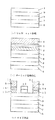
[ Reference Example 1] Reference Example 1 of the embodiment of the present invention will be described with reference to FIG. FIG. 1 shows a cross-sectional view of an n-type electrode structure according to an embodiment of the present invention and a reference example . First, an
[0018]
[ Reference Example 2] Reference Example 2 will be described below. The process up to the n-type electrode deposition is the same as in Reference Example 1 above. The heat treatment was performed at 100 ° C. for 30 minutes. As a result, good ohmic characteristics were obtained with good reproducibility.
[0019]
For Example 1 of an embodiment of Example 1 the present invention will be described with reference to FIG. The process up to electrode deposition is the same as in Reference Example 1 above. FIG. 2 shows a two-stage heat treatment method. The first stage temperature was 400 ° C. for 15 minutes, and the second stage temperature was 850 ° C. for 5 minutes. The characteristics of the n contact layer were measured using the electrode thus prepared. The results are shown in FIG. Good ohmic characteristics are obtained with good reproducibility, the
[0020]
[Embodiment 2 ] FIG. 10 shows an electrode formation process of a GaN field effect transistor (FET). First, crystal growth of GaN was performed using a gas source molecular beam epitaxial growth method. An ultra-high vacuum apparatus having a growth chamber and a patterning chamber is used.
[0021]
First, in the growth chamber, on an insulating sapphire substrate 6, radicalized nitrogen (3 × 10 - 6 Torr) and Ga - by molecular beam epitaxy using (5 × 10 7 Torr), at a growth temperature 640 ° C. thickness of 50 nm n - to form a
[0022]
Next, an electrode creation process using the above-described GaN epitaxial film will be described. The S i O 2 as a protective film GaN epi entire surface marked by a thermal chemical deposition method. Thereafter, patterning was performed using photolithography, and an opening was formed using hydrofluoric acid in a portion to be an electrode. Next, the
[0023]
Metal organic chemical vapor deposition (MOCVD) may be used for the growth of GaN. For forming the GaN film, dimethylhydrazine, monomethylhydrazine, ammonia or the like is used as a nitrogen source. As the Ga source, an organic metal gas such as triethylgallium or trimethylgallium is used. Moreover, monosilane, disilane, etc. are used as an n-type dopant.
[0024]
Further, the same effect can be obtained with the
[0025]
In addition to GaN, the same effect can be obtained in gallium nitride semiconductors such as GaAlN, InGaN, and InGaAlN.
[0026]
Moreover, although the GaN field effect transistor was shown in Example 2 , the same effect is acquired also in the n-type electrode utilized with a light emitting diode, a laser diode, etc.
[0027]
[Comparative example]
A comparative example of the present invention will be described with reference to FIG. FIG. 6 shows a cross-sectional view of a comparative n-type electrode structure. On the surface of the
[0028]
【The invention's effect】
As apparent from the above description, in the method for forming an electrode on the surface of the n-type gallium nitride compound semiconductor layer according to
[0029]
In addition, when electrodes are formed on a wafer having a diameter of 2 inches or more, the heat treatment temperature can be set particularly in a low temperature region, and troubles such as cracking and warping of the wafer can be prevented.
[Brief description of the drawings]
FIG. 1 is a cross-sectional view showing an n-type electrode structure according to Reference Examples 1 and 2 of the present invention.
FIG. 2 is a two-stage heat treatment method according to Examples 1 and 2 of the present invention.
3 is a cross-sectional view showing an n-type electrode structure of Conventional Example 1. FIG.
4 is a cross-sectional view showing an n-type electrode structure of Conventional Example 2. FIG.
FIG. 5 is a cross-sectional view showing an n-type electrode structure of a comparative example.
7 is a graph showing current-voltage characteristics of an electrode according to Reference Example 1 of the present invention. FIG.
FIG. 8 is a diagram showing current-voltage characteristics of an electrode according to Reference Example 2 of the present invention.
9 is a graph showing current-voltage characteristics of an electrode according to Comparative Example 1. FIG.
FIG. 10 is a diagram showing an electrode formation process of a GaN FET.
[Explanation of symbols]
1
Claims (1)
Priority Applications (1)
| Application Number | Priority Date | Filing Date | Title |
|---|---|---|---|
| JP2000002326A JP4494567B2 (en) | 2000-01-11 | 2000-01-11 | Method of forming electrode on n-type gallium nitride compound semiconductor layer |
Applications Claiming Priority (1)
| Application Number | Priority Date | Filing Date | Title |
|---|---|---|---|
| JP2000002326A JP4494567B2 (en) | 2000-01-11 | 2000-01-11 | Method of forming electrode on n-type gallium nitride compound semiconductor layer |
Publications (2)
| Publication Number | Publication Date |
|---|---|
| JP2001196574A JP2001196574A (en) | 2001-07-19 |
| JP4494567B2 true JP4494567B2 (en) | 2010-06-30 |
Family
ID=18531447
Family Applications (1)
| Application Number | Title | Priority Date | Filing Date |
|---|---|---|---|
| JP2000002326A Expired - Lifetime JP4494567B2 (en) | 2000-01-11 | 2000-01-11 | Method of forming electrode on n-type gallium nitride compound semiconductor layer |
Country Status (1)
| Country | Link |
|---|---|
| JP (1) | JP4494567B2 (en) |
Families Citing this family (14)
| Publication number | Priority date | Publication date | Assignee | Title |
|---|---|---|---|---|
| JP4023121B2 (en) | 2001-09-06 | 2007-12-19 | 豊田合成株式会社 | N-type electrode, group III nitride compound semiconductor device, method for manufacturing n-type electrode, and method for manufacturing group III nitride compound semiconductor device |
| KR100519753B1 (en) * | 2002-11-15 | 2005-10-07 | 삼성전기주식회사 | Method for manufacturing light emitting device comprising compound semiconductor of GaN group |
| US20090029353A1 (en) | 2003-12-08 | 2009-01-29 | Maki Wusi C | Molecular detector |
| CN100463243C (en) * | 2004-06-14 | 2009-02-18 | 北京大学 | Push-out light electrode and its production |
| CN100394560C (en) * | 2004-08-09 | 2008-06-11 | 中国科学院微电子研究所 | Al/Ti/Al/Ti/Au ohmic contact system adapted to GaN device |
| CN100367475C (en) * | 2004-08-09 | 2008-02-06 | 中国科学院微电子研究所 | Al/Ti/Al/Pt/Au ohmic contact system adapted to GaN device |
| CN100485886C (en) * | 2004-08-09 | 2009-05-06 | 中国科学院微电子研究所 | Al/Ti/Al/Ti/Pt/Au ohmic contact system adapted to GaN device |
| CN100481346C (en) * | 2004-08-09 | 2009-04-22 | 中国科学院微电子研究所 | Al/Ti/Al/Ni/Au ohmic contact system adapted to GaN device |
| US8766448B2 (en) | 2007-06-25 | 2014-07-01 | Sensor Electronic Technology, Inc. | Chromium/Titanium/Aluminum-based semiconductor device contact |
| US9064845B2 (en) | 2007-06-25 | 2015-06-23 | Sensor Electronic Technology, Inc. | Methods of fabricating a chromium/titanium/aluminum-based semiconductor device contact |
| JP2009124033A (en) * | 2007-11-16 | 2009-06-04 | Nippon Telegr & Teleph Corp <Ntt> | Semiconductor device, and its manufacturing method |
| JP6206159B2 (en) | 2013-12-17 | 2017-10-04 | 三菱電機株式会社 | Manufacturing method of semiconductor device |
| CN106972088B (en) * | 2017-05-25 | 2019-03-08 | 合肥彩虹蓝光科技有限公司 | A kind of LED metal electrode structure and preparation method thereof |
| CN108364864A (en) * | 2018-03-02 | 2018-08-03 | 华南理工大学 | The preparation method of AlGaN/GaN HEMT device Ohm contact electrodes |
Citations (2)
| Publication number | Priority date | Publication date | Assignee | Title |
|---|---|---|---|---|
| JPH08274372A (en) * | 1995-03-31 | 1996-10-18 | Toyoda Gosei Co Ltd | Group iii nitride semiconductor light emitting element |
| JPH10107316A (en) * | 1996-10-01 | 1998-04-24 | Toyoda Gosei Co Ltd | Semiconductor light-emitting device of iii group nitride |
-
2000
- 2000-01-11 JP JP2000002326A patent/JP4494567B2/en not_active Expired - Lifetime
Patent Citations (2)
| Publication number | Priority date | Publication date | Assignee | Title |
|---|---|---|---|---|
| JPH08274372A (en) * | 1995-03-31 | 1996-10-18 | Toyoda Gosei Co Ltd | Group iii nitride semiconductor light emitting element |
| JPH10107316A (en) * | 1996-10-01 | 1998-04-24 | Toyoda Gosei Co Ltd | Semiconductor light-emitting device of iii group nitride |
Also Published As
| Publication number | Publication date |
|---|---|
| JP2001196574A (en) | 2001-07-19 |
Similar Documents
| Publication | Publication Date | Title |
|---|---|---|
| US6358770B2 (en) | Method for growing nitride semiconductor crystals, nitride semiconductor device, and method for fabricating the same | |
| Fan et al. | Very low resistance multilayer Ohmic contact to n‐GaN | |
| JP5099008B2 (en) | Compound semiconductor device using SiC substrate and manufacturing method thereof | |
| JP2803741B2 (en) | Gallium nitride based compound semiconductor electrode forming method | |
| US7001791B2 (en) | GaN growth on Si using ZnO buffer layer | |
| JP4494567B2 (en) | Method of forming electrode on n-type gallium nitride compound semiconductor layer | |
| JP5242156B2 (en) | III-V nitride compound semiconductor device and electrode forming method | |
| JP3365607B2 (en) | GaN-based compound semiconductor device and method of manufacturing the same | |
| JP2010522434A (en) | Termination and contact structures for high voltage GaN based heterojunction transistors | |
| JP4023121B2 (en) | N-type electrode, group III nitride compound semiconductor device, method for manufacturing n-type electrode, and method for manufacturing group III nitride compound semiconductor device | |
| US20030124877A1 (en) | Method of heat-treating nitride compound semiconductor layer and method of producing semiconductor device | |
| JPH11145518A (en) | Manufacture of gallium nitride compound semiconductor | |
| JPH11177134A (en) | Manufacture of semiconductor element, semiconductor, manufacture of light emitting element, and light emitting element | |
| JP3557791B2 (en) | Group III nitride semiconductor electrode and device having the electrode | |
| US8431936B2 (en) | Method for fabricating a p-type semiconductor structure | |
| EP0825652B1 (en) | Ohmic electrode and method of forming the same | |
| JP2001102565A (en) | Method of manufacturing semiconductor device | |
| JP2927768B1 (en) | Semiconductor device and manufacturing method thereof | |
| US20020004254A1 (en) | Method for producing p-type gallium nitride-based compound semiconductor, method for producing gallium nitride-based compound semiconductor light-emitting device, and gallium nitride-based compound semiconductor light-emitting device | |
| JP3497790B2 (en) | Method for manufacturing p-type gallium nitride based semiconductor and light emitting device using p-type gallium nitride based semiconductor | |
| JP3703975B2 (en) | Gallium nitride compound semiconductor light emitting device | |
| EP1172867A2 (en) | Method for producing P-Type Gallium Nitride-Based compound semiconductor, method for producing Gallium Nitride-Based compound semiconductor light-emitting device, and gallium nitride-based compound semiconductor light-emitting device | |
| US6774025B2 (en) | Method for producing group III nitride compound semiconductor light-emitting element | |
| JP3599592B2 (en) | Method for forming electrode on group III-V nitride compound semiconductor | |
| JP3642199B2 (en) | Method for manufacturing gallium nitride compound semiconductor light emitting device |
Legal Events
| Date | Code | Title | Description |
|---|---|---|---|
| A621 | Written request for application examination |
Free format text: JAPANESE INTERMEDIATE CODE: A621 Effective date: 20060901 |
|
| A977 | Report on retrieval |
Free format text: JAPANESE INTERMEDIATE CODE: A971007 Effective date: 20080331 |
|
| A131 | Notification of reasons for refusal |
Free format text: JAPANESE INTERMEDIATE CODE: A131 Effective date: 20091201 |
|
| A521 | Written amendment |
Free format text: JAPANESE INTERMEDIATE CODE: A523 Effective date: 20100127 |
|
| A521 | Written amendment |
Free format text: JAPANESE INTERMEDIATE CODE: A523 Effective date: 20100215 |
|
| TRDD | Decision of grant or rejection written | ||
| A01 | Written decision to grant a patent or to grant a registration (utility model) |
Free format text: JAPANESE INTERMEDIATE CODE: A01 Effective date: 20100318 |
|
| A01 | Written decision to grant a patent or to grant a registration (utility model) |
Free format text: JAPANESE INTERMEDIATE CODE: A01 |
|
| A61 | First payment of annual fees (during grant procedure) |
Free format text: JAPANESE INTERMEDIATE CODE: A61 Effective date: 20100408 |
|
| R151 | Written notification of patent or utility model registration |
Ref document number: 4494567 Country of ref document: JP Free format text: JAPANESE INTERMEDIATE CODE: R151 |
|
| FPAY | Renewal fee payment (event date is renewal date of database) |
Free format text: PAYMENT UNTIL: 20130416 Year of fee payment: 3 |
|
| FPAY | Renewal fee payment (event date is renewal date of database) |
Free format text: PAYMENT UNTIL: 20130416 Year of fee payment: 3 |
|
| FPAY | Renewal fee payment (event date is renewal date of database) |
Free format text: PAYMENT UNTIL: 20140416 Year of fee payment: 4 |
|
| EXPY | Cancellation because of completion of term |