JP4486303B2 - Method for avoiding effects due to misalignment that can occur between vias and trenches in semiconductor device interconnect structures - Google Patents
Method for avoiding effects due to misalignment that can occur between vias and trenches in semiconductor device interconnect structures Download PDFInfo
- Publication number
- JP4486303B2 JP4486303B2 JP2002337918A JP2002337918A JP4486303B2 JP 4486303 B2 JP4486303 B2 JP 4486303B2 JP 2002337918 A JP2002337918 A JP 2002337918A JP 2002337918 A JP2002337918 A JP 2002337918A JP 4486303 B2 JP4486303 B2 JP 4486303B2
- Authority
- JP
- Japan
- Prior art keywords
- layer
- mask
- trench
- mask film
- forming
- Prior art date
- Legal status (The legal status is an assumption and is not a legal conclusion. Google has not performed a legal analysis and makes no representation as to the accuracy of the status listed.)
- Expired - Fee Related
Links
Images


Classifications
-
- H—ELECTRICITY
- H01—ELECTRIC ELEMENTS
- H01L—SEMICONDUCTOR DEVICES NOT COVERED BY CLASS H10
- H01L21/00—Processes or apparatus adapted for the manufacture or treatment of semiconductor or solid state devices or of parts thereof
- H01L21/02—Manufacture or treatment of semiconductor devices or of parts thereof
- H01L21/04—Manufacture or treatment of semiconductor devices or of parts thereof the devices having at least one potential-jump barrier or surface barrier, e.g. PN junction, depletion layer or carrier concentration layer
- H01L21/18—Manufacture or treatment of semiconductor devices or of parts thereof the devices having at least one potential-jump barrier or surface barrier, e.g. PN junction, depletion layer or carrier concentration layer the devices having semiconductor bodies comprising elements of Group IV of the Periodic System or AIIIBV compounds with or without impurities, e.g. doping materials
- H01L21/28—Manufacture of electrodes on semiconductor bodies using processes or apparatus not provided for in groups H01L21/20 - H01L21/268
-
- H—ELECTRICITY
- H01—ELECTRIC ELEMENTS
- H01L—SEMICONDUCTOR DEVICES NOT COVERED BY CLASS H10
- H01L21/00—Processes or apparatus adapted for the manufacture or treatment of semiconductor or solid state devices or of parts thereof
- H01L21/70—Manufacture or treatment of devices consisting of a plurality of solid state components formed in or on a common substrate or of parts thereof; Manufacture of integrated circuit devices or of parts thereof
- H01L21/71—Manufacture of specific parts of devices defined in group H01L21/70
- H01L21/768—Applying interconnections to be used for carrying current between separate components within a device comprising conductors and dielectrics
- H01L21/76801—Applying interconnections to be used for carrying current between separate components within a device comprising conductors and dielectrics characterised by the formation and the after-treatment of the dielectrics, e.g. smoothing
- H01L21/76802—Applying interconnections to be used for carrying current between separate components within a device comprising conductors and dielectrics characterised by the formation and the after-treatment of the dielectrics, e.g. smoothing by forming openings in dielectrics
- H01L21/76807—Applying interconnections to be used for carrying current between separate components within a device comprising conductors and dielectrics characterised by the formation and the after-treatment of the dielectrics, e.g. smoothing by forming openings in dielectrics for dual damascene structures
- H01L21/76811—Applying interconnections to be used for carrying current between separate components within a device comprising conductors and dielectrics characterised by the formation and the after-treatment of the dielectrics, e.g. smoothing by forming openings in dielectrics for dual damascene structures involving multiple stacked pre-patterned masks
-
- H—ELECTRICITY
- H01—ELECTRIC ELEMENTS
- H01L—SEMICONDUCTOR DEVICES NOT COVERED BY CLASS H10
- H01L21/00—Processes or apparatus adapted for the manufacture or treatment of semiconductor or solid state devices or of parts thereof
- H01L21/70—Manufacture or treatment of devices consisting of a plurality of solid state components formed in or on a common substrate or of parts thereof; Manufacture of integrated circuit devices or of parts thereof
- H01L21/71—Manufacture of specific parts of devices defined in group H01L21/70
- H01L21/768—Applying interconnections to be used for carrying current between separate components within a device comprising conductors and dielectrics
- H01L21/76801—Applying interconnections to be used for carrying current between separate components within a device comprising conductors and dielectrics characterised by the formation and the after-treatment of the dielectrics, e.g. smoothing
- H01L21/76802—Applying interconnections to be used for carrying current between separate components within a device comprising conductors and dielectrics characterised by the formation and the after-treatment of the dielectrics, e.g. smoothing by forming openings in dielectrics
- H01L21/76807—Applying interconnections to be used for carrying current between separate components within a device comprising conductors and dielectrics characterised by the formation and the after-treatment of the dielectrics, e.g. smoothing by forming openings in dielectrics for dual damascene structures
- H01L21/76813—Applying interconnections to be used for carrying current between separate components within a device comprising conductors and dielectrics characterised by the formation and the after-treatment of the dielectrics, e.g. smoothing by forming openings in dielectrics for dual damascene structures involving a partial via etch
Landscapes
- Engineering & Computer Science (AREA)
- Physics & Mathematics (AREA)
- Condensed Matter Physics & Semiconductors (AREA)
- General Physics & Mathematics (AREA)
- Manufacturing & Machinery (AREA)
- Computer Hardware Design (AREA)
- Microelectronics & Electronic Packaging (AREA)
- Power Engineering (AREA)
- Internal Circuitry In Semiconductor Integrated Circuit Devices (AREA)
Description
【0001】
【発明の属する技術分野】
本発明は、一般に半導体装置上の相互接続構造の製造に関する。より詳細には、本発明は、相互接続された構造の製造において使用される二重ダマシーン・プロセス(dual damascene process)に関係し、低k誘電体材料を組み込む相互接続構造に関係する。
【0002】
【従来の技術】
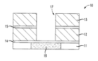
いくつかの異なる二重ダマシーン・プロセスが、相互接続構造の製造において使用されることができる。そのようなプロセスの1つが、図1から図4に示されている完全バイア・ファースト(Full Via−First、FVF)である。図1に示されるように、基板10は、エッチングの前に、金属相互接続フィーチャ(feature)18が形成された相互接続層11を有することができる。バリア層14が、層11およびフィーチャ18を覆う。中間エッチング停止層15で分離された、2つの誘電体層12および13がバリア層14を覆う。パターニングされたフォトレジスト(「PR」)層16が、上部誘電体層13上に堆積される。
【0003】
バイア・フィーチャが、フォトリソグラフィを使用して、装置または構造10のフォトレジスト層16にパターニングされる。図2に示されるように、バイア17が、誘電体層13および12と、エッチング停止層15とを介して、バリア層14までエッチングされる。フォトレジスト層16は、その後、半導体装置から剥離され、新規のすなわち新しいフォトレジスト層(図示せず)と置き換えられる。トレンチ・フィーチャは、新たなフォトレジスト層にパターニングされる。図3に示されるように、トレンチ18は、誘電体層13を介してエッチング停止層15までエッチングされる。その後、新たなフォトレジスト層は剥離される。バイア17内に露出された、エッチング停止層15および絶縁体バリア層14は、それから選択的にエッチングされる。銅フィルム19とともに薄い銅バリア(図示せず)が、その後トレンチ18およびバイア17内に堆積される。半導体装置は、図4に示される相互接続構造を形成するために、化学機械的な平坦化を用いて平坦化される。
【0004】
【発明が解決しようとする課題】
上述したように、バイア17が、誘電体層12および13を介してエッチングされた後、新たなフォトレジスト材料が、バイア17を充填して装置10上に堆積される。自己平坦化反射防止コーティング/フォトレジスト、すなわちARC/フォトレジストが、フォトリソグラフィ機器の十分な集束に関する平坦な表面を提供するために使用される。ARC/フォトレジストの使用のいくつかの欠点は、バイアが完全に明瞭にされる補償なしに、マイクロ・トレンチ形成の可能性、およびバイア内のARCの除去に必要なエッチング時間全体の延長を含む。これらの問題は、歩留まりの減少およびより低い信頼性の装置を招く可能性がある。
【0005】
他の問題は、「低k誘電体材料」内のアミン不純物と、ARC/フォトレジストとの相互作用の存在である。より低い誘電率を有する誘電体材料は、低k誘電体材料として知られており、半導体装置の相互接続構造の製造においてますます一般的になっている。低k誘電体材料は、一般に、約3.0までの誘電率を有する。しかしながら、低k誘電体材料は、フォトレジスト材料と化学的に反応する、またはフォトレジスト材料が低k誘電体材料と接触するとき、フォトレジスト材料と反応する不純物を有する。
【0006】
低k誘電体材料とフォトレジスト材料との間の反応は、表面相互作用とは別に、バイア内でも相互作用が存在するトレンチ形成の間ではより重大である。その後、フォトレジスト材料と低k誘電体材料との間の反応は、トレンチのパターニングを遮断し、かつ従来のFVF二重ダマシーン・プロセスを用いる相互接続構造の製造を妨げる。
【0007】
これらの欠点は、二重ダマシーン・プロセスの代わりを使用することを招き、かつ低k誘電体材料上に堆積されるマスク層(また「ハード・マスク層」として参照される)の使用を組み込む。本明細書において使用されるマスク層は、フィルムまたは複合フィルムを含み、相互接続構造における誘電体材料を覆い、かつフォトレジストと誘電体材料との間のバリア層として作用する層である。マスク層は、また、ハード・マスク層またはフォトレジスト・マスクとして参照されることができ、これらの用語は、本開示において交換可能に使用されることができる。マスク層は、エッチング・プロセスの間に誘電体材料の特定領域を保護する。
【0008】
従来技術において知られているハード・マスク層は、一般的には、異なる特性のフィルムの2つの層を含む。2つのマスク・フィルムは、通常SiCまたはSi3N4からなる第1のマスク・フィルムと、二酸化シリコン(SiO2)からなる第2のマスク・フィルムとを含むことができる。2つのハード・マスク・フィルムは、バイアおよびトレンチのフォトリソグラフィおよびエッチングの間に、フォトレジスト材料が低k誘電体材料と接触することを防ぐ。さらに、第1のマスク・フィルム、すなわちSiCまたはSi3N4は、低k誘電体フィルムを、化学機械的研磨から保護する。また、第1のマスク・フィルムは、トレンチまたはバイアに堆積されるべき金属フィルムに関する、絶縁体または拡散バリアとして作用し、その機能は、表面電流または金属イオン・リークを、トレンチ内に堆積された導電金属から防ぐことである。第2のハード・マスク・フィルムは、犠牲層(sacrificial layer)として作用し、トレンチまたはバイアは、初期的にエッチングされ、かつ全てのプロセスの完了後に排除される。誘電体層上のバイアまたはトレンチ・パターンが、下の誘電体層に移されたとき、下の誘電体層の保護を助ける。
【0009】
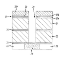
マスク層を組み込む二重ダマシーン・プロセスは、2層ハード・マスクにおける部分的トレンチ・ファースト(partial−trench−first)(「PTF−2LM」としても参照される)、および2層ハード・マスクにおける部分的バイア・ファースト(partial−via−first)(「PVF−2LM」としても参照される)である。PTF−2LM二重ダマシーン・プロセスが、図5〜図8に示されている。図5に示される半導体装置20は、導電ライン24を有する下の相互接続層23を覆って堆積された、バイア誘電体層22およびトレンチ誘電体層21を備える誘電体材料を含む。絶縁バリア層25は、金属層23とバイア誘電体層22との間に配置される。エッチング停止層26は、バイア誘電体層22とトレンチ誘電体層21との間に配置される。第1のマスク・フィルム27Aおよび第2のマスク・フィルム27Bを有するマスク層27は、誘電体材料を覆う。フォトレジスト層28が、トレンチ・フーチャをパターニングするために、マスク層上に堆積される。
【0010】
図6を参照すると、トレンチ・フィーチャに関する場所は、まずフォトレジスト層28にパターニングされ、その後、第2のマスク・フィルム27Bを介して第1のマスク・フィルム27Aまでエッチングされる。フォトレジスト層28は、それから取り除かれ、トレンチ30を充填する新たなフォトレジスト層28Aで置き換えられる。図7に関して、バイア29のフィーチャは、新たなフォトレジスト層28Aにパターニングされ、かつ誘電体層21および22を介して絶縁体バリア層25までエッチングされる。新たなフォトレジスト層28は、それから剥離される。
【0011】
図8に示されるように、マスク層27にパターニングされかつエッチングされるトレンチ30のフィーチャは、その後、トレンチ誘電体層21を介してエッチング停止層26までエッチングされる。フォトレジスト材料の保護は存在しないので、トレンチ誘電体層21がエッチングされるとき、マスク層の新たなマスク・フィルムがエッチングされないように、エッチング薬品は選択される。別々のエッチング処置で、トレンチ30内のエッチング停止層26、およびバイア29内のバリア絶縁体層25は、選択的にエッチングされ(図示せず)、バイア29は、下の導電ライン24をトレンチ30内に形成される導電ラインと接続することができる。
【0012】
バイア29は、導電ライン24をトレンチ30内に形成されたラインに接続する。最適な製造歩留まりと信頼性とを達成するために、バイアおよびトレンチ・フィーチャは、十分にアライメントしなければならない。上述のPTF−2LHM二重ダマシーン・プロセスにおいて、トレンチ30は、まず、下の金属ライン24とアライメントされ、その後、バイア29が、トレンチ30または金属ライン24とアライメントされる。金属ライン24とのトレンチ30とのミスアライメントは、バイア29のアライメントまたは接続性に影響を与える。バイア29が、トレンチ30に対してミスアライメントされると、誤差が増す。ミスアライメントされた相互接続のフィーチャは、漏れ電流、バイア抵抗値、およびバイア・チェーン抵抗値を増加する結果になることがあり、これらは全て、歩留まり損失を引き起こす。
【0013】
したがって、まず、バイアを下の金属ラインとアライメントし、これをエッチングすることが好ましく、これは、図9〜図12に示されるように、PVF−2LHM二重ダマシーン・プロセスにおいてなされる。バイア39のフィーチャは、フォトレジスト層31にパターニングされ、その後、二重マスク層32の第2のマスク・フィルム32Bにエッチングされる。フォトレジスト層31は、剥離され、新たなフォトレジスト層46と置き換えられる。トレンチ30のフィーチャは、それから、新たなフォトレジスト層46にパターニングされる。バイア39は、まず、第1のマスク・フィルム32Aに対して選択的であるエッチング薬品を使用して、マスク層32の第1のマスク・フィルム32Aを介して、トレンチ誘電体33の所定の深さまでエッチングされる。フォトレジスト46におけるトレンチ30のフィーチャは、マスク層32の第2のマスク・フィルム32Bにエッチングされる。それから、バイア39は、図11に示されるように、バイア誘電体層34を介して絶縁体バリア層37までエッチングされる。図12に関して、トレンチ30は、その後、フォトレジスト層に前にパターニングされ、かつマスク層32の第2のマスク・フィルム32Bにエッチングされたフィーチャに従って、トレンチ誘電体層33を介してエッチングされる。別々のエッチング処置において、トレンチ30内のエッチング停止層38およびバイア39内のバリア絶縁体層37は、選択的にエッチングされる。それから、バイア39は、下の導電ライン36をトレンチ30に形成された導電ラインに接続する。
【0014】
PVF−2LHM二重ダマシーン・プロセスにおけるミスアライメントは、バイアの低減された幅の結果になることがある。図13に関して、半導体装置は、第1のマスク・フィルム40Aおよび第2のマスク・フィルム40Bを有するマスク層40の所定の深さまでエッチングされたバイア41を有して示されている。フォトレジスト層42は、マスク層40上に堆積され、トレンチ・フィーチャ43は、第2のマスク・フィルム40Bを介してフォトレジスト層42にパターニングされて示されている。図13において破線で示されるように、トレンチ・フィーチャ43は、マスク層40内の部分的エッチングされたバイア41に関してミスアライメントされている。バイア41が、その後、フォトレジスト42および誘電体材料中にエッチングされるとき、バイア41の寸法は、誘電体材料で完全にエッチングされない。図14における破線は、バイア41の最初にパターニングされた寸法を示している。しかしながら、最初のバイア41の寸法が、新たなフォトレジスト層42内でパターニングされたトレンチのフィーチャ43内に無いので、バイア41の全体寸法は、誘電体材料中にエッチングされることができない。したがって、バイアのサイズは、低減される。トレンチ45は、それから、誘電体材料でエッチングされ、ミスアライメントの結果として、導電ライン44の側方に変位する。バイアの寸法における低減は、バイア・コンタクトおよびチェーン抵抗値を増大し、かつ装置の信頼性および歩留まりを低下させる可能性がある。
【0015】
【課題を解決するための手段】
本発明は、相互接続構造の二重ダマシーン製造における新規なマスク層の使用によって、上述の問題を解決するものである。マスク層は、特に、低k誘電体材料で有用であることができる。本明細書で使用される低k誘電体材料または低k誘電体層は、低k有機珪酸塩の誘電体材料、および約3までの誘電率を有する有機誘電体材料を含む。
【0016】
マスク層は、下の金属層を覆う誘電体材料上に堆積される。マスク層は、絶縁フィルムおよび/またはパッシベーション層(また、「パッシベーション・マスク・フィルム」としても参照される)として作用する第1のマスク・フィルムを含む、4つのマスク・フィルムを有する。第2のマスク・フィルム、第3のマスク・フィルム、および第4のマスク・フィルムを含む3つのマスク・フィルムは、第1のマスク・フィルム上に堆積される。
【0017】
マスク・フィルムの組成は、第1のマスク・フィルムが、第3のマスク・フィルムのエッチング特性と実質的に同一のエッチング特性を有し、一方、第2のマスク・フィルムが、第4のマスク・フィルムのエッチング特性と実質的に同一のエッチング特性を有するようなものである。本明細書で使用される「エッチング特性」との用語は、所定のエッチング薬品および/またはエッチング処置に対する、エッチング速度およびエッチング選択性を含む、フィルムまたは層組成のエッチング特性である。
【0018】
第1のマスク・フィルムおよび第3のマスク・フィルムは、マスク・フィルムに関する知られているフィルム組成であるSiO2またはSiCを含む。代わりに、これらのマスク・フィルムは、誘電体材料に対して許容可能なエッチング選択性を有する、SiN4または何らかの他の適切な組成を含むことができる。第2のマスク・フィルムおよび第4のマスク・フィルムは、同様に誘電体材料に関して適切なエッチング選択性を有するように選択された材料から構成される。
【0019】
二重ダマシーン・プロセスを用いて、バイアのフィーチャおよびトレンチのフィーチャは、パターニングされ、その後、マスク層でエッチングされる。バイアのフィーチャは、マスク層の所定の深さまで、あるいは最初の3つのフィルムを介してエッチングされる。トレンチのフィーチャは、同様に、マスク・フィルムの所定の深さまでであるが、第1のマスク・フィルムだけを介してエッチングされる。二重ダマシーン・プロセスは、部分的バイア・ファースト(すなわち「PVF」)処置を組み込むことができ、PVF処置において、部分的トレンチ・ファースト(「PTF」)処置のミスアライメント問題を避けるために、バイアは、トレンチの前にマスク層に形成される。
【0020】
バイアおよび/またはトレンチは、両方のバイアおよびトレンチが、第1にマスク層内にエッチングされるまで、下の誘電体材料に移されず、任意のフォトレジスト材料は、装置から剥離されない。このように、バイアは、下の相互接続層におけるトレンチとのトレンチのミスアライメントにもかかわらず、バイアの幅の低減なしに、誘電体材料へ完全に移されることができる。
【0021】
バイアおよびトレンチは、それから、マスク層にパターニングされかつエッチングされたフィーチャに従って、誘電体材料でエッチングされる。犠牲フィルムは、選択されたフィルムまたは層のエッチング特性に応じて、バイア、トレンチ、エッチング停止層、または絶縁体バリアのエッチング・ステップの間、または、プロセスが完了したときの化学機械的な研磨の間に取り除かれる。バイアおよびトレンチが、誘電体層内でエッチングされ、かつ導電金属が誘電体層に堆積された後、導電金属は、相互接続構造を完了するために、化学機械的な平坦化を用いて平坦化される。
【0022】
本発明のより良い理解のために、添付の図面とともになされる以下の詳細で参照される。
【0023】
【発明の実施の形態】
集積回路装置または構造の相互接続層の断面図が、図1に示され、導電金属54を有する下の相互接続層53を覆って形成されるバイア誘電体層51およびトレンチ誘電体層52を含む、低k誘電体材料を含む。本明細書で使用されるバイア誘電体は、バイアが形成される誘電体層の部分を言及する。トレンチ誘電体は、トレンチが形成される誘電体層の部分を言及する。まず、バイア誘電体層51が、バリア層55上に堆積される。バイア誘電体層51は、任意の有機珪酸塩、または約3.0までの誘電率を有する有機低k誘電体材料を含むことができる。標準的な誘電体材料およびそのような使用される低k誘電体材料は、Novellus製のCORAL、Applied Materials製のBLACK DIAMOND、またはDow Chemical Company,Inc.製のSILKである。エッチング停止層56は、その後、バイア誘電体層51を覆って堆積される。トレンチ誘電体層52が、エッチング停止層56上に形成され、バイア誘電体層51において使用される同じ誘電体材料を含む。
【0024】
バイア誘電体層51は、一般に、約3000から約6000Aの厚み範囲にあることができ、トレンチ誘電体層52は、約1500Aから約6000Aの厚みの範囲にあることができる。エッチング停止層56および絶縁体バリア層55は、約500Aまでの範囲の厚みを有する。
【0025】
これらのフィルム厚みの例は、そのような厚みの範囲に本発明を限定するものではない。絶縁バリア層55は、一般に、窒化シリコン(Si3N4)または炭化シリコン(SiC)を含む。二酸化シリコンは、一般に、バリア層のための許容可能な組成ではない、しかしながら、エッチング停止層は、SiO2、Si3N4、またはSiCを含む3つの組成のいずれかを含むことができる。
【0026】
マスク層57は、その後、トレンチ誘電体層52を覆って堆積される。マスク層57は、誘電体材料と、マスク層57上に堆積されたフォトレジスト層62との間のバリアとして作用する。図15に示されるマスク層57は、第1のマスク・フィルム58、第2のマスク・フィルム59、第3のマスク・フィルム60、および第4のマスク・フィルム61を含む、4つのマスク・フィルムを有する。マスク・フィルム58〜61は、それぞれ約200Aから1000Aの厚み範囲であり、マスク層にパターニングされたバイアまたはトレンチ・フィーチャを、下の誘電体材料に効率的に移すために、誘電体材料に関して十分に高いエッチング選択性を有する材料を備える。例えば、マスク・フィルムは、一般にSi3N4、SiO2、またはSiCからなる。
【0027】
より詳細に説明されるように、本発明において、第1のマスク・フィルム58は、所定のエッチング薬品および/または処置に関してエッチング特性を有さなければならず、このエッチング特性は、第3のマスク・フィルム60のエッチング特性と実質的に同一である。同様に、第2のマスク・フィルム59は、第4のマスク・フィルム61のエッチング特性と実質的に同一であるエッチング特性を有さなければならない。第1のマスク・フィルム58が、Si3N4からなるなら、第3のマスク・フィルム60は、好ましくはSi3N4からなり、第2のマスク・フィルム59が、SiO2またはSiCからなるなら、第4のマスク・フィルム61は、好ましくはSiO2またはSiCからなる。したがって、マスク・フィルム58〜61の組成およびエッチング特性は、第1のマスク・フィルム58から第4のマスク・フィルム61へと交互にするべきである。
【0028】
第1のマスク・フィルム58は、パッシベーション層である。定義によって、パッシベーション層は、下の誘電体層51および52を汚染から保護する。さらに、第1のマスク・フィルム58は、絶縁体として作用する。第1のマスク・フィルム58は、相互接続構造の部品のままであり、導電ライン間の表面電流漏れを防止する。第1のマスク・フィルム58は、パッシベーション・マスク・フィルムとして言及されることができる。
【0029】
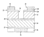
本発明の二重ダマシーン・プロセスは、図16から図25に示されている。本発明の二重ダマシーン・プロセスは、一般に、上述された2層ハード・マスク機構を有する部分的バイア・ファーストに従うが、4層ハード・マスクの使用の結果としていくつかの点で区別可能である。まず、バイア・フィーチャは、フォトレジスト層62にパターニングされ、バイア63は、第1のマスク・フィルム58へ下方にマスク層57でエッチングされる。それから、フォトレジスト層62は、図17に示されるように剥離される。新たなフォトレジスト層64は、バイア63を充填するマスク層57上に形成される。それから、トレンチ・フィーチャは、フォトレジスト層64でパターニングされる。図18に示されるように、それから、トレンチ65は、第3のマスク・フィルム60へ下方にマスク層57でエッチングされる。
【0030】
本発明において、マスク層57は、2つの追加のマスク・フィルムを有し、マスク層57は、バイア63およびトレンチ65が下の誘電体材料中にエッチングされる前に、トレンチ65が、マスク層57でエッチングされることを可能にする。図19に示されるように、フィーチャ63および65が誘電体材料でエッチングされる前に、フォトレジスト層64が取り除かれる。より詳細に説明されるように、マスク層57においてトレンチ65を省くことは、バイアの寸法の低減を避ける。
【0031】
図20に関して、バイア63の寸法内に残っている第1のマスク・フィルム58のその部分は、エッチングされ、トレンチ65の寸法内の第3のマスク・フィルム60のその部分は、同様に単一のステップでエッチングされる。上述のように、第1のマスク・フィルム58および第3のマスク・フィルム60は、同様のエッチング特性およびエッチング速度を有し、同一の組成からなり、マスク・フィルム56および60のこれらの部分は、同一のエッチング・ステップで取り除かれる。
【0032】
図21において、バイア63は、マスク層57およびトレンチ誘電体層52を介して、エッチング停止層56までエッチングされる。誘電体材料でエッチングされたバイアととともに、犠牲フィルム59〜61は、順次取り除かれることができる。しかしながら、トレンチ・フィーチャは、トレンチ65を下の誘電体材料に移すためにマスク層57に維持される。図22に示されるように、第4のマスク・フィルム61は、トレンチ65がマスク・フィルム59でエッチングされたとき、第4のマスク・フィルム61は取り除かれる。第2のマスク・フィルム59が、ほとんど第4のマスク・フィルム61のエッチング特性と同一のエッチング特性を有するなら、トレンチ65のパターン内の第2のマスク・フィルム59の部分は、同様に取り除かれる。
【0033】
さらに、示された実施形態におけるエッチング停止層は、第2のマスク・フィルムおよび第4のマスク・フィルム61のエッチング特性と類似するエッチング特性を有する。したがって、第4のマスク・フィルム61および第2のマスク・フィルム69の部分が、図23に示されるように取り除かれたとき、エッチング停止層56は取り除かれる。代わりに、エッチング停止層が、第1のマスク・フィルムおよび第3のマスク・フィルム60のエッチング特性と類似するエッチング特性を有する材料からなるなら、マスク・フィルム58および60の部分は、エッチング停止層のエッチング処置の間に取り除かれることができる。
【0034】
別々のステップにおいて、部分的トレンチ65における第1のマスク・フィルム58の部分は取り除かれ、第1のマスク・フィルム58、第2のマスク・フィルム59、および第3のマスク・フィルム60が、トレンチ65を画定する。
【0035】
その後、バイア63は、バリア層55に下方へバイア誘電体層51を介してエッチングされ、トレンチ65は、図24に示されるようにトレンチ誘電体層52を介して同時にエッチングされる。その後、バリア層55は、図25に示されるように、導電ライン54を露出するために選択的にエッチングされ、第3のマスク・フィルム60に関する残っている部分は、取り除かれることができる。マスク層57の唯一の残っているマスク・フィルムは、第1のマスク・フィルム58および第2のマスク・フィルム59である。第1のマスク・フィルム58は、パッシベーション層であり、処理後に装置構造の一部となる。
【0036】
図26に示されるように、導電金属66が、バイア63およびトレンチ65に堆積される。まず、薄い銅バリア層および銅シード層が、スパッタリングまたは化学的気相成長技術(CVD)を用いて堆積され、電気めっきを用いてバイア63およびトレンチ65を充填するために、薄い銅フィルム堆積がこれらの層に続く。化学機械的な平坦化(Chemical Mechanical Planarization、CMP)が、トレンチ65の外部の過剰な導電金属を除去し、かつマスク・フィルム59〜60の残りを取り除くために使用され、第1のマスク・フィルム58は、導電金属66に隣接して残る。このように、図26に示される相互接続構造は、二重ダマシーン処置を使用して形成され、下の導電ライン54とトレンチ65内に形成された導電ラインとを電気的に接続するバイア63を含む。
【0037】
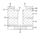
図27〜29に関して、トレンチ・フィーチャ69が、フォトレジスト層67にパターニングされたとき、バイア68に対してミスアライメントされて示されている。まず、バイア68は、フォトレジスト層にパターニングされ、マスク層66でエッチングされる。フォトレジスト層は取り除かれ、図27に示されるように、フォトレジスト層67と置き換えられる。破線で示されるトレンチ・フィーチャ69は、フォトレジスト層67でパターニングされる。しかしながら、トレンチ・フィーチャは、ミスアライメントされ、またはバイア68の側方に変位される。
【0038】
その後、トレンチ75は、フォトレジスト層67を介して、および第4のマスク・フィルム73を介してマスク層66へエッチングされる。フォトレジスト層67が、図29に示されるように取り除かれたとき、バイア68およびトレンチ75は、マスク層66に形成される。フォトレジスト材料が、バイア68から取り除かれ、トレンチ75のミスアライメントは、バイア68の寸法の低減を結果として生じない。
【0039】
本発明において、トレンチ75が、マスク層66でパターニングされ、トレンチおよびバイアがさらにエッチングされる前に、フォトレジスト層は、装置から剥離されることができる。フォトレジスト層67が取り除かれたとき、バイア68の全体幅は、エッチング処置に露出され、したがって、たとえトレンチがミスアライメントされていても、バイアの寸法は低減されることはできない。
【0040】
本発明の好ましい実施形態が、示され、かつ本明細書においてこれに関連して説明されたが、そのような実施形態が、例示のためだけに与えられ限定するものではないことは、明らかである。多数の変形、変更、および置換は、本明細書における本発明から逸脱することなく当業者には可能である。例えば、本明細書に開示された最良の形態に必ずしも限定されない。なぜなら、他の適用は、本発明の教示から等しく恩恵を受けることが可能である。したがって、本発明は、請求項の精神および範囲によってのみ限定される。
【図面の簡単な説明】
【図1】完全バイア・ファースト二重ダマシーン・プロセスを示す図である。
【図2】完全バイア・ファースト二重ダマシーン・プロセスを示す図である。
【図3】完全バイア・ファースト二重ダマシーン・プロセスを示す図である。
【図4】完全バイア・ファースト二重ダマシーン・プロセスを示す図である。
【図5】2層ハード・マスクを有する部分的トレンチ・ファースト(PTF−2LHM)二重ダマシーン・プロセスを示す図である。
【図6】2層ハード・マスクを有する部分的トレンチ・ファースト(PTF−2LHM)二重ダマシーン・プロセスを示す図である。
【図7】2層ハード・マスクを有する部分的トレンチ・ファースト(PTF−2LHM)二重ダマシーン・プロセスを示す図である。
【図8】2層ハード・マスクを有する部分的トレンチ・ファースト(PTF−2LHM)二重ダマシーン・プロセスを示す図である。
【図9】2層ハード・マスクを有する部分的バイア・ファースト(PVF−2LHM)二重ダマシーン・プロセスを示す図である。
【図10】2層ハード・マスクを有する部分的バイア・ファースト(PVF−2LHM)二重ダマシーン・プロセスを示す図である。
【図11】2層ハード・マスクを有する部分的バイア・ファースト(PVF−2LHM)二重ダマシーン・プロセスを示す図である。
【図12】2層ハード・マスクを有する部分的バイア・ファースト(PVF−2LHM)二重ダマシーン・プロセスを示す図である。
【図13】バイアの寸法が低減されるPVF−2LHM二重ダマシーン・プロセスを示す図である。
【図14】バイアの寸法が低減されるPVF−2LHM二重ダマシーン・プロセスを示す図である。
【図15】本発明の新規なマスク層および二重ダマシーン・プロセスを示す図である。
【図16】本発明の新規なマスク層および二重ダマシーン・プロセスを示す図である。
【図17】本発明の新規なマスク層および二重ダマシーン・プロセスを示す図である。
【図18】本発明の新規なマスク層および二重ダマシーン・プロセスを示す図である。
【図19】本発明の新規なマスク層および二重ダマシーン・プロセスを示す図である。
【図20】本発明の新規なマスク層および二重ダマシーン・プロセスを示す図である。
【図21】本発明の新規なマスク層および二重ダマシーン・プロセスを示す図である。
【図22】本発明の新規なマスク層および二重ダマシーン・プロセスを示す図である。
【図23】本発明の新規なマスク層および二重ダマシーン・プロセスを示す図である。
【図24】本発明の新規なマスク層および二重ダマシーン・プロセスを示す図である。
【図25】本発明の新規なマスク層および二重ダマシーン・プロセスを示す図である。
【図26】本発明の新規なマスク層および二重ダマシーン・プロセスを示す図である。
【図27】トレンチが半導体装置上でミスアライメントされたときの、本発明の新規なマスク層および二重ダマシーン・プロセスを示す図である。
【図28】トレンチが半導体装置上でミスアライメントされたときの、本発明の新規なマスク層および二重ダマシーン・プロセスを示す図である。
【図29】トレンチが半導体装置上でミスアライメントされたときの、本発明の新規なマスク層および二重ダマシーン・プロセスを示す図である。[0001]
BACKGROUND OF THE INVENTION
The present invention relates generally to the manufacture of interconnect structures on semiconductor devices. More particularly, the present invention relates to a dual damascene process used in the manufacture of interconnected structures, and to interconnect structures that incorporate low-k dielectric materials.
[0002]
[Prior art]
Several different dual damascene processes can be used in the manufacture of the interconnect structure. One such process is Full Via-First (FVF) as shown in FIGS. As shown in FIG. 1, the
[0003]
Via features are patterned into the
[0004]
[Problems to be solved by the invention]
As described above, after via 17 has been etched through
[0005]
Another problem is the presence of an ARC / photoresist interaction with amine impurities in the “low-k dielectric material”. Dielectric materials having lower dielectric constants are known as low-k dielectric materials and are becoming increasingly common in the fabrication of semiconductor device interconnect structures. Low-k dielectric materials generally have a dielectric constant up to about 3.0. However, the low-k dielectric material has impurities that react chemically with the photoresist material or react with the photoresist material when the photoresist material contacts the low-k dielectric material.
[0006]
The reaction between the low-k dielectric material and the photoresist material is more critical during trench formation where the interaction exists within the via, as well as the surface interaction. Thereafter, the reaction between the photoresist material and the low-k dielectric material blocks the trench patterning and prevents fabrication of the interconnect structure using a conventional FVF dual damascene process.
[0007]
These drawbacks lead to the use of a dual damascene process and incorporate the use of a mask layer (also referred to as a “hard mask layer”) deposited on a low-k dielectric material. As used herein, a mask layer is a layer that includes a film or composite film, covers the dielectric material in the interconnect structure, and acts as a barrier layer between the photoresist and the dielectric material. A mask layer can also be referred to as a hard mask layer or a photoresist mask, and these terms can be used interchangeably in this disclosure. The mask layer protects certain areas of the dielectric material during the etching process.
[0008]
The hard mask layers known in the prior art generally comprise two layers of films with different properties. The two mask films are usually SiC or Si 3 N 4 A first mask film comprising silicon dioxide (SiO 2) 2 2) a second mask film. The two hard mask films prevent the photoresist material from contacting the low-k dielectric material during via and trench photolithography and etching. Furthermore, a first mask film, ie SiC or Si 3 N 4 Protects low-k dielectric films from chemical mechanical polishing. The first mask film also acts as an insulator or diffusion barrier for the metal film to be deposited in the trench or via, whose function is to deposit surface current or metal ion leakage into the trench. It is to prevent from conductive metal. The second hard mask film acts as a sacrificial layer, and the trenches or vias are initially etched and eliminated after completion of all processes. When the via or trench pattern on the dielectric layer is transferred to the lower dielectric layer, it helps protect the lower dielectric layer.
[0009]
A dual damascene process that incorporates a mask layer is a partial trench-first (also referred to as “PTF-2LM”) in a two-layer hard mask, and a portion in a two-layer hard mask. Partial-via-first (also referred to as “PVF-2LM”). The PTF-2LM dual damascene process is shown in FIGS. The
[0010]
Referring to FIG. 6, the location for the trench feature is first patterned into the
[0011]
As shown in FIG. 8, the features of the
[0012]
Via 29 connects
[0013]
Therefore, it is preferred to first align the via with the underlying metal line and etch it, which is done in a PVF-2LHM dual damascene process, as shown in FIGS. The features of the via 39 are patterned into the
[0014]
Misalignment in the PVF-2LHM dual damascene process can result in reduced via width. With reference to FIG. 13, a semiconductor device is shown having a via 41 etched to a predetermined depth of a
[0015]
[Means for Solving the Problems]
The present invention solves the above problems by the use of a novel mask layer in the fabrication of interconnected dual damascenes. The mask layer can be particularly useful with low-k dielectric materials. As used herein, a low-k dielectric material or layer includes a low-k organosilicate dielectric material and an organic dielectric material having a dielectric constant up to about 3.
[0016]
A mask layer is deposited on the dielectric material covering the underlying metal layer. The mask layer has four mask films, including a first mask film that acts as an insulating film and / or a passivation layer (also referred to as a “passivation mask film”). Three mask films, including a second mask film, a third mask film, and a fourth mask film are deposited on the first mask film.
[0017]
The composition of the mask film is such that the first mask film has substantially the same etching characteristics as the third mask film, while the second mask film is the fourth mask. -It has an etching characteristic substantially the same as the etching characteristic of the film. The term “etch characteristics” as used herein is an etch characteristic of a film or layer composition, including etch rate and etch selectivity for a given etch chemistry and / or etch procedure.
[0018]
The first mask film and the third mask film are SiO, which is a known film composition for mask films. 2 Alternatively, SiC is included. Instead, these mask films are SiN with acceptable etch selectivity to dielectric materials. 4 Or any other suitable composition may be included. The second mask film and the fourth mask film are similarly composed of materials selected to have appropriate etch selectivity with respect to the dielectric material.
[0019]
Using a dual damascene process, via features and trench features are patterned and then etched with a mask layer. Via features are etched to a predetermined depth in the mask layer or through the first three films. The trench features are similarly etched to a predetermined depth of the mask film but only through the first mask film. The dual damascene process can incorporate partial via first (ie, “PVF”) procedures, and to avoid misalignment problems with partial trench first (“PTF”) procedures in PVF procedures. Is formed in the mask layer before the trench.
[0020]
Vias and / or trenches are not transferred to the underlying dielectric material and any photoresist material is not stripped from the device until both vias and trenches are first etched into the mask layer. In this way, the via can be completely transferred to the dielectric material without a reduction in the width of the via, despite trench misalignment with the trench in the underlying interconnect layer.
[0021]
Vias and trenches are then etched with a dielectric material according to the features patterned and etched into the mask layer. The sacrificial film may be subjected to chemical mechanical polishing during via, trench, etch stop layer, or insulator barrier etch steps, or when the process is complete, depending on the etching characteristics of the selected film or layer. Removed in between. After vias and trenches are etched in the dielectric layer and conductive metal is deposited on the dielectric layer, the conductive metal is planarized using chemical mechanical planarization to complete the interconnect structure. Is done.
[0022]
For a better understanding of the present invention, reference is made to the following details taken in conjunction with the accompanying drawings.
[0023]
DETAILED DESCRIPTION OF THE INVENTION
A cross-sectional view of an interconnect layer of an integrated circuit device or structure is shown in FIG. 1 and includes a via
[0024]
Via
[0025]
These examples of film thickness do not limit the invention to such thickness ranges. The insulating
[0026]
A
[0027]
As will be described in more detail, in the present invention, the
[0028]
The
[0029]
The dual damascene process of the present invention is illustrated in FIGS. The dual damascene process of the present invention generally follows partial via first with the two-layer hard mask mechanism described above, but is distinguishable in several ways as a result of the use of a four-layer hard mask. . First, the via features are patterned into the
[0030]
In the present invention, the
[0031]
With reference to FIG. 20, that portion of the
[0032]
In FIG. 21, via 63 is etched to etch
[0033]
Furthermore, the etch stop layer in the illustrated embodiment has an etching characteristic similar to that of the second mask film and the
[0034]
In separate steps, the portion of the
[0035]
Thereafter, the via 63 is etched down into the
[0036]
As shown in FIG. 26,
[0037]
With reference to FIGS. 27-29, trench feature 69 is shown misaligned with respect to via 68 when patterned into
[0038]
Thereafter, the
[0039]
In the present invention, the photoresist layer can be stripped from the device before
[0040]
While preferred embodiments of the invention have been shown and described herein in connection therewith, it is obvious that such embodiments are given by way of example only and are not limiting. is there. Numerous variations, modifications, and substitutions are possible to those skilled in the art without departing from the invention herein. For example, the present invention is not necessarily limited to the best mode disclosed herein. Because other applications can equally benefit from the teachings of the present invention. Accordingly, the invention is limited only by the spirit and scope of the following claims.
[Brief description of the drawings]
FIG. 1 illustrates a complete via first dual damascene process.
FIG. 2 illustrates a full via first dual damascene process.
FIG. 3 illustrates a full via first dual damascene process.
FIG. 4 illustrates a full via first dual damascene process.
FIG. 5 illustrates a partial trench first (PTF-2LHM) dual damascene process with a two layer hard mask.
FIG. 6 illustrates a partial trench first (PTF-2LHM) dual damascene process with a two layer hard mask.
FIG. 7 illustrates a partial trench first (PTF-2LHM) dual damascene process with a two layer hard mask.
FIG. 8 illustrates a partial trench first (PTF-2LHM) dual damascene process with a two layer hard mask.
FIG. 9 illustrates a partial via first (PVF-2LHM) dual damascene process with a two layer hard mask.
FIG. 10 illustrates a partial via first (PVF-2LHM) dual damascene process with a two layer hard mask.
FIG. 11 illustrates a partial via first (PVF-2LHM) dual damascene process with a two layer hard mask.
FIG. 12 illustrates a partial via first (PVF-2LHM) dual damascene process with a two layer hard mask.
FIG. 13 illustrates a PVF-2LHM dual damascene process in which via dimensions are reduced.
FIG. 14 illustrates a PVF-2LHM dual damascene process in which via dimensions are reduced.
FIG. 15 illustrates the novel mask layer and dual damascene process of the present invention.
FIG. 16 illustrates the novel mask layer and dual damascene process of the present invention.
FIG. 17 illustrates the novel mask layer and dual damascene process of the present invention.
FIG. 18 illustrates the novel mask layer and dual damascene process of the present invention.
FIG. 19 illustrates the novel mask layer and dual damascene process of the present invention.
FIG. 20 illustrates the novel mask layer and dual damascene process of the present invention.
FIG. 21 illustrates the novel mask layer and dual damascene process of the present invention.
FIG. 22 illustrates the novel mask layer and dual damascene process of the present invention.
FIG. 23 illustrates the novel mask layer and dual damascene process of the present invention.
FIG. 24 illustrates the novel mask layer and dual damascene process of the present invention.
FIG. 25 illustrates the novel mask layer and dual damascene process of the present invention.
FIG. 26 illustrates the novel mask layer and dual damascene process of the present invention.
FIG. 27 illustrates the novel mask layer and dual damascene process of the present invention when the trench is misaligned on the semiconductor device.
FIG. 28 illustrates the novel mask layer and dual damascene process of the present invention when the trench is misaligned on the semiconductor device.
FIG. 29 illustrates the novel mask layer and dual damascene process of the present invention when trenches are misaligned on a semiconductor device.
Claims (11)
(a)所定のエッチング特性を有する該誘電体材料の上に第1のマスク膜を形成するステップ、
(b)該第1のマスク膜のエッチング特性とは異なる所定のエッチング特性を有する第2のマスク膜を該第1のマスク膜の上に形成するステップ、
(c)該第1のマスク膜のエッチング特性と同一のエッチング特性を有する第3のマスク膜を該第2のマスク膜の上に形成するステップ、
(d)該第2のマスク膜のエッチング特性と同一のエッチング特性を有する第4のマスク膜を該第3のマスク膜の上に形成するステップ、
(e)該第2、第3および第4のマスク膜をエッチングして、第1の所定の深さを有し、かつ該第1のマスク膜の表面に至るバイアを、下に位置する誘電体層を露出させることなく、該マスク層内にバイアを形成するステップ、
(f)該第4のマスク膜をエッチングして、該マスク層内において前にエッチングされたマスク層の該第1の所定の深さよりも浅い第2の深さまで、下に位置する誘電体材料を露出させることなく、該マスク層内にトレンチを形成するステップ、
(g)該マスク層内に形成されたバイアの寸法に対応する、該誘電体材料を通るバイアを形成すると共に、該マスク層内に形成されたトレンチの寸法に対応するトレンチを、該誘電体材料中に所定の深さのところまで形成するステップ、及び
(h)マスク層内の該バイアと該トレンチの間にミスアライメントが生じる場合に、該マスク層内の該バイアから該ミスアライメントに因るそのバイア中に残されたフォトレジスト材料を取り除き、これにより該マスク層内の該バイアをその元のサイズに回復させるようにするステップ
を含むことを特徴とする方法。To avoid the effects due to misalignment that can occur between vias and trenches in the interconnect structure using a mask layer deposited on the dielectric layer deposited on the underlying interconnect layer The method of
(A) forming a first mask film on the dielectric material having predetermined etching characteristics;
(B) forming a second mask film having a predetermined etching characteristic different from the etching characteristic of the first mask film on the first mask film;
(C) forming a third mask film on the second mask film having the same etching characteristics as the etching characteristics of the first mask film;
(D) forming a fourth mask film having the same etching characteristics as the etching characteristics of the second mask film on the third mask film;
(E) Dielectric that etches the second, third, and fourth mask films to have a first predetermined depth and a via that reaches the surface of the first mask film underneath Forming a via in the mask layer without exposing the body layer;
(F) etching the fourth mask film to a dielectric material located below to a second depth shallower than the first predetermined depth of the previously etched mask layer in the mask layer; Forming a trench in the mask layer without exposing
(G) forming a via through the dielectric material corresponding to a dimension of a via formed in the mask layer and a trench corresponding to a dimension of a trench formed in the mask layer; Forming to a predetermined depth in the material; and (h) due to misalignment from the via in the mask layer if a misalignment occurs between the via in the mask layer and the trench. Removing the photoresist material left in the via, thereby allowing the via in the mask layer to recover to its original size.
該マスク層内に形成された該バイアおよびトレンチが、該ミスアライメントが生じ得る該相互接続構造中の該バイアおよびトレンチを構成するものである方法。The method of claim 1, wherein
The method wherein the vias and trenches formed in the mask layer constitute the vias and trenches in the interconnect structure where misalignment can occur.
該第1のマスク膜をエッチングして、該マスク層中の該バイアを処理して該下に位置する誘電体材料を露出させると共に、該第3のマスク膜をエッチングして、該第2のマスク膜の表面に至るトレンチを該マスク層中に形成するステップを含む方法。The method of claim 1, further comprising: etching the first mask film to treat the vias in the mask layer to expose the underlying dielectric material; and Etching the film to form a trench in the mask layer leading to the surface of the second mask film.
該誘電体材料を通るバイアを形成するステップ、および該第1のマスク膜の表面に至るトレンチを該マスク層中に形成した後に、該誘電体材料中に誘電体材料の所定の厚さのトレンチを形成するステップを含む方法。4. The method of claim 3, further comprising: forming a via through the dielectric material; and forming a trench in the mask layer leading to the surface of the first mask film, and then in the dielectric material. Forming a trench of a predetermined thickness of dielectric material.
該半導体デバイスから該第3および第4のマスク膜を取り除くステップを含む方法。5. The method of claim 4, further comprising removing the third and fourth mask films from the semiconductor device.
該半導体デバイスから該第2、第3および第4のマスク膜を取り除くステップを含む方法。5. The method of claim 4, further comprising removing the second, third and fourth mask films from the semiconductor device.
該下に位置する相互接続層の上にバイア誘電体層を形成するステップ、該バイア誘導体層の上にトレンチ層を形成するステップ、および該誘電体層と該トレンチ層の間にエッチング停止層を形成するステップを含む方法。4. The method of claim 3, further comprising: forming a via dielectric layer over the underlying interconnect layer; forming a trench layer over the via dielectric layer; and the dielectric layer; Forming an etch stop layer between the trench layers.
該マスク層中に形成された該バイアの寸法に従って、該トレンチ層中に該バイアをエッチングして、ついで、該エッチング停止層をエッチングする処理と、該第4のマスク膜を該半導体デバイスから取り除く処理とを同時に行うステップを含む方法。The method of claim 7, further comprising: etching the via into the trench layer according to the size of the via formed in the mask layer, and then etching the etch stop layer; And a step of simultaneously removing the mask film of 4 from the semiconductor device.
該バイア誘電体層と該相互接続層の間にバリア層を形成するステップを含む方法。The method of claim 7, further comprising forming a barrier layer between the via dielectric layer and the interconnect layer.
該マスク層中に形成された該バイアの寸法に従って、該バイア誘電体層を該バリア層のところまでエッチングし、ついで、該バリア層をエッチングする処理と、該第3のマスク膜を該半導体デバイスから取り除く処理とを同時に行うステップを含む方法。The method of claim 9, further comprising: etching the via dielectric layer to the barrier layer according to the size of the via formed in the mask layer, and then etching the barrier layer; And a step of simultaneously performing a process of removing the third mask film from the semiconductor device.
該トレンチ誘電体層中に該トレンチを形成し、および該バリア層をエッチングする前に該バイア誘電体層中に該バイアを同時に形成するステップを含む方法。The method of claim 10, further comprising the step of forming the trench in the trench dielectric layer and simultaneously forming the via in the via dielectric layer prior to etching the barrier layer.
Applications Claiming Priority (2)
| Application Number | Priority Date | Filing Date | Title |
|---|---|---|---|
| US10/026,257 US20030119305A1 (en) | 2001-12-21 | 2001-12-21 | Mask layer and dual damascene interconnect structure in a semiconductor device |
| US10/026257 | 2001-12-21 |
Related Child Applications (1)
| Application Number | Title | Priority Date | Filing Date |
|---|---|---|---|
| JP2009161396A Division JP2009224816A (en) | 2001-12-21 | 2009-07-08 | Mask layer and dual damascene interconnect structure in semiconductor device |
Publications (3)
| Publication Number | Publication Date |
|---|---|
| JP2003197738A JP2003197738A (en) | 2003-07-11 |
| JP2003197738A5 JP2003197738A5 (en) | 2006-01-12 |
| JP4486303B2 true JP4486303B2 (en) | 2010-06-23 |
Family
ID=21830765
Family Applications (2)
| Application Number | Title | Priority Date | Filing Date |
|---|---|---|---|
| JP2002337918A Expired - Fee Related JP4486303B2 (en) | 2001-12-21 | 2002-11-21 | Method for avoiding effects due to misalignment that can occur between vias and trenches in semiconductor device interconnect structures |
| JP2009161396A Pending JP2009224816A (en) | 2001-12-21 | 2009-07-08 | Mask layer and dual damascene interconnect structure in semiconductor device |
Family Applications After (1)
| Application Number | Title | Priority Date | Filing Date |
|---|---|---|---|
| JP2009161396A Pending JP2009224816A (en) | 2001-12-21 | 2009-07-08 | Mask layer and dual damascene interconnect structure in semiconductor device |
Country Status (5)
| Country | Link |
|---|---|
| US (2) | US20030119305A1 (en) |
| JP (2) | JP4486303B2 (en) |
| KR (1) | KR20030053055A (en) |
| GB (1) | GB2390741B (en) |
| TW (1) | TWI254375B (en) |
Families Citing this family (40)
| Publication number | Priority date | Publication date | Assignee | Title |
|---|---|---|---|---|
| JP2003282704A (en) * | 2002-03-26 | 2003-10-03 | Nec Electronics Corp | Method of manufacturing semiconductor device with dual-damacene |
| US6815333B2 (en) * | 2002-04-02 | 2004-11-09 | Dow Global Technologies Inc. | Tri-layer masking architecture for patterning dual damascene interconnects |
| US7265431B2 (en) * | 2002-05-17 | 2007-09-04 | Intel Corporation | Imageable bottom anti-reflective coating for high resolution lithography |
| JP4104426B2 (en) * | 2002-10-30 | 2008-06-18 | 富士通株式会社 | Manufacturing method of semiconductor device |
| US6767825B1 (en) * | 2003-02-03 | 2004-07-27 | United Microelectronics Corporation | Etching process for forming damascene structure of the semiconductor |
| KR100487948B1 (en) * | 2003-03-06 | 2005-05-06 | 삼성전자주식회사 | Method of forming a via contact structure using a dual damascene technique |
| US7217649B2 (en) * | 2003-03-14 | 2007-05-15 | Lam Research Corporation | System and method for stress free conductor removal |
| US7232766B2 (en) * | 2003-03-14 | 2007-06-19 | Lam Research Corporation | System and method for surface reduction, passivation, corrosion prevention and activation of copper surface |
| US7078344B2 (en) * | 2003-03-14 | 2006-07-18 | Lam Research Corporation | Stress free etch processing in combination with a dynamic liquid meniscus |
| US7009281B2 (en) * | 2003-03-14 | 2006-03-07 | Lam Corporation | Small volume process chamber with hot inner surfaces |
| JP3757213B2 (en) * | 2003-03-18 | 2006-03-22 | 富士通株式会社 | Manufacturing method of semiconductor device |
| WO2004097923A1 (en) | 2003-04-30 | 2004-11-11 | Fujitsu Limited | Method for fabricating semiconductor device |
| WO2005071752A1 (en) * | 2004-01-14 | 2005-08-04 | International Business Machines Corporation | Gradient deposition of low-k cvd materials |
| JP4160569B2 (en) * | 2004-05-31 | 2008-10-01 | 株式会社東芝 | Manufacturing method of semiconductor device |
| JP2006024811A (en) * | 2004-07-09 | 2006-01-26 | Sony Corp | Method for manufacturing semiconductor device |
| US7999392B2 (en) | 2005-03-09 | 2011-08-16 | Renesas Electronics Corporation | Multilayer wiring structure, semiconductor device, pattern transfer mask and method for manufacturing multilayer wiring structure |
| JP4476171B2 (en) | 2005-05-30 | 2010-06-09 | 富士通マイクロエレクトロニクス株式会社 | Manufacturing method of semiconductor device |
| US7781892B2 (en) * | 2005-12-22 | 2010-08-24 | Taiwan Semiconductor Manufacturing Company, Ltd. | Interconnect structure and method of fabricating same |
| US20090014887A1 (en) * | 2006-01-06 | 2009-01-15 | Nec Corporation | Method of producing multilayer interconnection and multilayer interconnection structure |
| US20070249165A1 (en) * | 2006-04-05 | 2007-10-25 | Huang Chun-Jen | Dual damascene process |
| US7855142B2 (en) * | 2009-01-09 | 2010-12-21 | Samsung Electronics Co., Ltd. | Methods of forming dual-damascene metal interconnect structures using multi-layer hard masks |
| KR200453906Y1 (en) * | 2009-07-08 | 2011-06-02 | 주식회사 이노디자인 | Folding helmat |
| US8404581B2 (en) * | 2009-09-29 | 2013-03-26 | Taiwan Semiconductor Manufacturing Company, Ltd. | Method of forming an interconnect of a semiconductor device |
| DE102010038736A1 (en) * | 2010-07-30 | 2012-02-02 | Globalfoundries Dresden Module One Llc & Co. Kg | A method of controlling the critical dimensions of trenches in a metallization system of a semiconductor device during the etching of an etch stop layer |
| CN102487036B (en) * | 2010-12-01 | 2014-09-03 | 中芯国际集成电路制造(北京)有限公司 | Manufacturing method of interconnection structure |
| JP6061610B2 (en) * | 2012-10-18 | 2017-01-18 | ルネサスエレクトロニクス株式会社 | Manufacturing method of semiconductor device |
| US8668835B1 (en) | 2013-01-23 | 2014-03-11 | Lam Research Corporation | Method of etching self-aligned vias and trenches in a multi-layer film stack |
| US8906810B2 (en) | 2013-05-07 | 2014-12-09 | Lam Research Corporation | Pulsed dielectric etch process for in-situ metal hard mask shape control to enable void-free metallization |
| US20140342553A1 (en) * | 2013-05-14 | 2014-11-20 | United Microelectronics Corp. | Method for Forming Semiconductor Structure Having Opening |
| US9305839B2 (en) * | 2013-12-19 | 2016-04-05 | Taiwan Semiconductor Manufacturing Company, Ltd. | Curing photo resist for improving etching selectivity |
| US9385000B2 (en) * | 2014-01-24 | 2016-07-05 | United Microelectronics Corp. | Method of performing etching process |
| US9522844B2 (en) * | 2014-09-03 | 2016-12-20 | Shenzhen China Star Optoelectronics Technology Co., Ltd. | Low temperature poly-silicon thin film preparation apparatus and method for preparing the same |
| US9786491B2 (en) | 2015-11-12 | 2017-10-10 | Asm Ip Holding B.V. | Formation of SiOCN thin films |
| KR102547096B1 (en) | 2015-12-22 | 2023-06-26 | 에스케이하이닉스 주식회사 | Method for manufacturing dual damascene structure |
| KR102378021B1 (en) | 2016-05-06 | 2022-03-23 | 에이에스엠 아이피 홀딩 비.브이. | Formation of SiOC thin films |
| US9964587B2 (en) | 2016-05-11 | 2018-05-08 | United Microelectronics Corp. | Semiconductor structure and testing method using the same |
| CN107492517B (en) * | 2016-06-12 | 2020-05-08 | 中芯国际集成电路制造(上海)有限公司 | Interconnect structure and method of formation |
| US10847529B2 (en) * | 2017-04-13 | 2020-11-24 | Asm Ip Holding B.V. | Substrate processing method and device manufactured by the same |
| CN110546302B (en) | 2017-05-05 | 2022-05-27 | Asm Ip 控股有限公司 | Plasma enhanced deposition method for controlled formation of oxygen-containing films |
| US10991573B2 (en) | 2017-12-04 | 2021-04-27 | Asm Ip Holding B.V. | Uniform deposition of SiOC on dielectric and metal surfaces |
Family Cites Families (15)
| Publication number | Priority date | Publication date | Assignee | Title |
|---|---|---|---|---|
| US5821169A (en) * | 1996-08-05 | 1998-10-13 | Sharp Microelectronics Technology,Inc. | Hard mask method for transferring a multi-level photoresist pattern |
| US5882996A (en) * | 1997-10-14 | 1999-03-16 | Industrial Technology Research Institute | Method of self-aligned dual damascene patterning using developer soluble arc interstitial layer |
| US6127263A (en) * | 1998-07-10 | 2000-10-03 | Applied Materials, Inc. | Misalignment tolerant techniques for dual damascene fabrication |
| US6156643A (en) * | 1998-11-06 | 2000-12-05 | Advanced Micro Devices, Inc. | Method of forming a dual damascene trench and borderless via structure |
| US6312874B1 (en) * | 1998-11-06 | 2001-11-06 | Advanced Micro Devices, Inc. | Method for forming a dual damascene trench and underlying borderless via in low dielectric constant materials |
| US6309962B1 (en) * | 1999-09-15 | 2001-10-30 | Taiwan Semiconductor Manufacturing Company | Film stack and etching sequence for dual damascene |
| US6331479B1 (en) * | 1999-09-20 | 2001-12-18 | Chartered Semiconductor Manufacturing Ltd. | Method to prevent degradation of low dielectric constant material in copper damascene interconnects |
| DE19958904C2 (en) * | 1999-12-07 | 2002-01-24 | Infineon Technologies Ag | Method of making a hard mask on a substrate |
| FR2802336B1 (en) * | 1999-12-13 | 2002-03-01 | St Microelectronics Sa | DAMASCENE-TYPE INTERCONNECTION STRUCTURE AND ITS MANUFACTURING METHOD |
| US6559070B1 (en) * | 2000-04-11 | 2003-05-06 | Applied Materials, Inc. | Mesoporous silica films with mobile ion gettering and accelerated processing |
| JP2001308179A (en) * | 2000-04-25 | 2001-11-02 | Sharp Corp | Method of manufacturing semiconductor device |
| JP4377040B2 (en) * | 2000-07-24 | 2009-12-02 | Necエレクトロニクス株式会社 | Semiconductor manufacturing method |
| US6537908B2 (en) * | 2001-02-28 | 2003-03-25 | International Business Machines Corporation | Method for dual-damascence patterning of low-k interconnects using spin-on distributed hardmask |
| US6603204B2 (en) | 2001-02-28 | 2003-08-05 | International Business Machines Corporation | Low-k interconnect structure comprised of a multilayer of spin-on porous dielectrics |
| US20030064582A1 (en) * | 2001-09-28 | 2003-04-03 | Oladeji Isaiah O. | Mask layer and interconnect structure for dual damascene semiconductor manufacturing |
-
2001
- 2001-12-21 US US10/026,257 patent/US20030119305A1/en not_active Abandoned
-
2002
- 2002-11-19 GB GB0226986A patent/GB2390741B/en not_active Expired - Fee Related
- 2002-11-21 JP JP2002337918A patent/JP4486303B2/en not_active Expired - Fee Related
- 2002-11-21 TW TW091133996A patent/TWI254375B/en not_active IP Right Cessation
- 2002-12-20 KR KR1020020081701A patent/KR20030053055A/en active Search and Examination
-
2003
- 2003-11-25 US US10/721,126 patent/US7067419B2/en not_active Expired - Fee Related
-
2009
- 2009-07-08 JP JP2009161396A patent/JP2009224816A/en active Pending
Also Published As
| Publication number | Publication date |
|---|---|
| GB0226986D0 (en) | 2002-12-24 |
| JP2009224816A (en) | 2009-10-01 |
| TW200301523A (en) | 2003-07-01 |
| US20040121579A1 (en) | 2004-06-24 |
| JP2003197738A (en) | 2003-07-11 |
| US20030119305A1 (en) | 2003-06-26 |
| US7067419B2 (en) | 2006-06-27 |
| TWI254375B (en) | 2006-05-01 |
| GB2390741B (en) | 2005-10-12 |
| GB2390741A (en) | 2004-01-14 |
| KR20030053055A (en) | 2003-06-27 |
Similar Documents
| Publication | Publication Date | Title |
|---|---|---|
| JP4486303B2 (en) | Method for avoiding effects due to misalignment that can occur between vias and trenches in semiconductor device interconnect structures | |
| KR100487948B1 (en) | Method of forming a via contact structure using a dual damascene technique | |
| US8299617B2 (en) | Method and apparatus for forming metal-metal oxide etch stop/barrier for integrated circuit interconnects | |
| JP4162241B2 (en) | Damascene interconnects and via liners using sacrificial inorganic polymer intermetallic dielectrics | |
| JP4250006B2 (en) | Semiconductor device and manufacturing method thereof | |
| EP1064674B1 (en) | A method of manufacturing an electronic device comprising two layers of organic-containing material | |
| JP4169150B2 (en) | Method of forming a metal pattern using a sacrificial hard mask | |
| KR100416596B1 (en) | Method of manufacturing interconnection wire in semiconductor device | |
| US6268283B1 (en) | Method for forming dual damascene structure | |
| US20060151887A1 (en) | Interconnection structure having double diffusion barrier layer and method of fabricating the same | |
| JP4193438B2 (en) | Manufacturing method of semiconductor device | |
| US20070232048A1 (en) | Damascene interconnection having a SiCOH low k layer | |
| US20040171256A1 (en) | Mask layer and interconnect structure for dual damascene semiconductor manufacturing | |
| US20070072334A1 (en) | Semiconductor fabrication process employing spacer defined vias | |
| US6849536B2 (en) | Inter-metal dielectric patterns and method of forming the same | |
| JP2004055781A (en) | Method for manufacturing semiconductor device | |
| KR100783868B1 (en) | A method of manufacturing a semiconductor device and a semiconductor device | |
| JP5047504B2 (en) | Method for manufacturing dual damascene wiring of semiconductor device using via capping protective film | |
| KR20050114784A (en) | Method for forming cu interconnection of semiconductor device | |
| US7279415B2 (en) | Method for forming a metallization layer stack to reduce the roughness of metal lines | |
| US7662711B2 (en) | Method of forming dual damascene pattern | |
| KR100784105B1 (en) | Method of manufacturing a semiconductor device | |
| KR20060026223A (en) | Fabrication method of dual damascene interconnection of microelectronic device and dual damascene interconnection structure | |
| KR20110075399A (en) | Method for fabricating dual damascene trench |
Legal Events
| Date | Code | Title | Description |
|---|---|---|---|
| A521 | Written amendment |
Free format text: JAPANESE INTERMEDIATE CODE: A523 Effective date: 20051117 |
|
| A621 | Written request for application examination |
Free format text: JAPANESE INTERMEDIATE CODE: A621 Effective date: 20051117 |
|
| A977 | Report on retrieval |
Free format text: JAPANESE INTERMEDIATE CODE: A971007 Effective date: 20070906 |
|
| A131 | Notification of reasons for refusal |
Free format text: JAPANESE INTERMEDIATE CODE: A131 Effective date: 20090408 |
|
| A521 | Written amendment |
Free format text: JAPANESE INTERMEDIATE CODE: A523 Effective date: 20090708 |
|
| A131 | Notification of reasons for refusal |
Free format text: JAPANESE INTERMEDIATE CODE: A131 Effective date: 20090909 |
|
| A521 | Written amendment |
Free format text: JAPANESE INTERMEDIATE CODE: A523 Effective date: 20090914 |
|
| A131 | Notification of reasons for refusal |
Free format text: JAPANESE INTERMEDIATE CODE: A131 Effective date: 20091116 |
|
| A521 | Written amendment |
Free format text: JAPANESE INTERMEDIATE CODE: A523 Effective date: 20091120 |
|
| TRDD | Decision of grant or rejection written | ||
| A01 | Written decision to grant a patent or to grant a registration (utility model) |
Free format text: JAPANESE INTERMEDIATE CODE: A01 Effective date: 20100303 |
|
| A01 | Written decision to grant a patent or to grant a registration (utility model) |
Free format text: JAPANESE INTERMEDIATE CODE: A01 |
|
| A61 | First payment of annual fees (during grant procedure) |
Free format text: JAPANESE INTERMEDIATE CODE: A61 Effective date: 20100326 |
|
| R150 | Certificate of patent or registration of utility model |
Free format text: JAPANESE INTERMEDIATE CODE: R150 |
|
| FPAY | Renewal fee payment (event date is renewal date of database) |
Free format text: PAYMENT UNTIL: 20130402 Year of fee payment: 3 |
|
| FPAY | Renewal fee payment (event date is renewal date of database) |
Free format text: PAYMENT UNTIL: 20130402 Year of fee payment: 3 |
|
| FPAY | Renewal fee payment (event date is renewal date of database) |
Free format text: PAYMENT UNTIL: 20140402 Year of fee payment: 4 |
|
| R250 | Receipt of annual fees |
Free format text: JAPANESE INTERMEDIATE CODE: R250 |
|
| LAPS | Cancellation because of no payment of annual fees |