JP4480410B2 - Organic semiconductor material, organic thin film transistor, and manufacturing method thereof - Google Patents
Organic semiconductor material, organic thin film transistor, and manufacturing method thereof Download PDFInfo
- Publication number
- JP4480410B2 JP4480410B2 JP2004024878A JP2004024878A JP4480410B2 JP 4480410 B2 JP4480410 B2 JP 4480410B2 JP 2004024878 A JP2004024878 A JP 2004024878A JP 2004024878 A JP2004024878 A JP 2004024878A JP 4480410 B2 JP4480410 B2 JP 4480410B2
- Authority
- JP
- Japan
- Prior art keywords
- group
- substituted
- general formula
- repeating unit
- unit represented
- Prior art date
- Legal status (The legal status is an assumption and is not a legal conclusion. Google has not performed a legal analysis and makes no representation as to the accuracy of the status listed.)
- Expired - Lifetime
Links
- 239000004065 semiconductor Substances 0.000 title claims description 98
- 239000000463 material Substances 0.000 title claims description 78
- 239000010409 thin film Substances 0.000 title claims description 37
- 238000004519 manufacturing process Methods 0.000 title claims description 25
- 229920000642 polymer Polymers 0.000 claims description 70
- 125000000217 alkyl group Chemical group 0.000 claims description 61
- UHOVQNZJYSORNB-UHFFFAOYSA-N Benzene Chemical compound C1=CC=CC=C1 UHOVQNZJYSORNB-UHFFFAOYSA-N 0.000 claims description 54
- 125000003545 alkoxy group Chemical group 0.000 claims description 54
- 125000004414 alkyl thio group Chemical group 0.000 claims description 51
- 239000010408 film Substances 0.000 claims description 51
- 238000000034 method Methods 0.000 claims description 41
- YTPLMLYBLZKORZ-UHFFFAOYSA-N Thiophene Chemical compound C=1C=CSC=1 YTPLMLYBLZKORZ-UHFFFAOYSA-N 0.000 claims description 38
- 125000005843 halogen group Chemical group 0.000 claims description 38
- MWPLVEDNUUSJAV-UHFFFAOYSA-N anthracene Chemical compound C1=CC=CC2=CC3=CC=CC=C3C=C21 MWPLVEDNUUSJAV-UHFFFAOYSA-N 0.000 claims description 36
- 150000001875 compounds Chemical class 0.000 claims description 36
- ZUOUZKKEUPVFJK-UHFFFAOYSA-N diphenyl Chemical compound C1=CC=CC=C1C1=CC=CC=C1 ZUOUZKKEUPVFJK-UHFFFAOYSA-N 0.000 claims description 36
- 125000001424 substituent group Chemical group 0.000 claims description 34
- -1 9-anthryl group Chemical group 0.000 claims description 24
- 239000002904 solvent Substances 0.000 claims description 23
- 229930192474 thiophene Natural products 0.000 claims description 19
- 125000003118 aryl group Chemical group 0.000 claims description 18
- 239000004305 biphenyl Substances 0.000 claims description 18
- 235000010290 biphenyl Nutrition 0.000 claims description 18
- 125000002029 aromatic hydrocarbon group Chemical group 0.000 claims description 17
- 125000004435 hydrogen atom Chemical group [H]* 0.000 claims description 12
- 239000000203 mixture Substances 0.000 claims description 11
- HEDRZPFGACZZDS-UHFFFAOYSA-N Chloroform Chemical compound ClC(Cl)Cl HEDRZPFGACZZDS-UHFFFAOYSA-N 0.000 claims description 10
- XEEYBQQBJWHFJM-UHFFFAOYSA-N Iron Chemical compound [Fe] XEEYBQQBJWHFJM-UHFFFAOYSA-N 0.000 claims description 8
- 125000004432 carbon atom Chemical group C* 0.000 claims description 7
- 125000003367 polycyclic group Chemical group 0.000 claims description 7
- 125000002950 monocyclic group Chemical group 0.000 claims description 5
- 230000008569 process Effects 0.000 claims description 5
- 125000000609 carbazolyl group Chemical group C1(=CC=CC=2C3=CC=CC=C3NC12)* 0.000 claims description 3
- 125000004122 cyclic group Chemical group 0.000 claims description 3
- BLRPTPMANUNPDV-UHFFFAOYSA-N Silane Chemical compound [SiH4] BLRPTPMANUNPDV-UHFFFAOYSA-N 0.000 claims description 2
- 230000008878 coupling Effects 0.000 claims description 2
- 238000010168 coupling process Methods 0.000 claims description 2
- 238000005859 coupling reaction Methods 0.000 claims description 2
- 239000012212 insulator Substances 0.000 claims description 2
- 229910000077 silane Inorganic materials 0.000 claims description 2
- WYURNTSHIVDZCO-UHFFFAOYSA-N Tetrahydrofuran Chemical compound C1CCOC1 WYURNTSHIVDZCO-UHFFFAOYSA-N 0.000 description 24
- 239000000243 solution Substances 0.000 description 24
- YXFVVABEGXRONW-UHFFFAOYSA-N Toluene Chemical compound CC1=CC=CC=C1 YXFVVABEGXRONW-UHFFFAOYSA-N 0.000 description 15
- 230000015572 biosynthetic process Effects 0.000 description 14
- 239000000758 substrate Substances 0.000 description 14
- 238000000576 coating method Methods 0.000 description 12
- 230000007613 environmental effect Effects 0.000 description 12
- YLQBMQCUIZJEEH-UHFFFAOYSA-N tetrahydrofuran Natural products C=1C=COC=1 YLQBMQCUIZJEEH-UHFFFAOYSA-N 0.000 description 12
- 230000008859 change Effects 0.000 description 11
- 239000011248 coating agent Substances 0.000 description 11
- XUIMIQQOPSSXEZ-UHFFFAOYSA-N Silicon Chemical compound [Si] XUIMIQQOPSSXEZ-UHFFFAOYSA-N 0.000 description 10
- 229910052710 silicon Inorganic materials 0.000 description 10
- 239000010703 silicon Substances 0.000 description 10
- 238000001035 drying Methods 0.000 description 9
- 238000004528 spin coating Methods 0.000 description 9
- 229910004298 SiO 2 Inorganic materials 0.000 description 8
- 238000006243 chemical reaction Methods 0.000 description 8
- 238000011156 evaluation Methods 0.000 description 8
- 238000003786 synthesis reaction Methods 0.000 description 8
- 230000000052 comparative effect Effects 0.000 description 7
- 0 C*C=C[C@](C1)C(OCCC(C)CCCC(C)C)=CC(C=Cc(cc2)ccc2N(c2ccc(C)cc2)c2ccc(C(C)C)cc2)=C1OC Chemical compound C*C=C[C@](C1)C(OCCC(C)CCCC(C)C)=CC(C=Cc(cc2)ccc2N(c2ccc(C)cc2)c2ccc(C(C)C)cc2)=C1OC 0.000 description 6
- YMWUJEATGCHHMB-UHFFFAOYSA-N Dichloromethane Chemical compound ClCCl YMWUJEATGCHHMB-UHFFFAOYSA-N 0.000 description 6
- URLKBWYHVLBVBO-UHFFFAOYSA-N Para-Xylene Chemical group CC1=CC=C(C)C=C1 URLKBWYHVLBVBO-UHFFFAOYSA-N 0.000 description 6
- 239000010931 gold Substances 0.000 description 6
- SLIUAWYAILUBJU-UHFFFAOYSA-N pentacene Chemical compound C1=CC=CC2=CC3=CC4=CC5=CC=CC=C5C=C4C=C3C=C21 SLIUAWYAILUBJU-UHFFFAOYSA-N 0.000 description 6
- 230000005669 field effect Effects 0.000 description 5
- 239000011368 organic material Substances 0.000 description 5
- 239000003960 organic solvent Substances 0.000 description 5
- 125000001997 phenyl group Chemical group [H]C1=C([H])C([H])=C(*)C([H])=C1[H] 0.000 description 5
- 238000007639 printing Methods 0.000 description 5
- 239000007787 solid Substances 0.000 description 5
- ZNZYKNKBJPZETN-WELNAUFTSA-N Dialdehyde 11678 Chemical class N1C2=CC=CC=C2C2=C1[C@H](C[C@H](/C(=C/O)C(=O)OC)[C@@H](C=C)C=O)NCC2 ZNZYKNKBJPZETN-WELNAUFTSA-N 0.000 description 4
- 239000004793 Polystyrene Substances 0.000 description 4
- 239000012298 atmosphere Substances 0.000 description 4
- 230000008901 benefit Effects 0.000 description 4
- 238000007254 oxidation reaction Methods 0.000 description 4
- 229920002223 polystyrene Polymers 0.000 description 4
- 239000000523 sample Substances 0.000 description 4
- QTBSBXVTEAMEQO-UHFFFAOYSA-N Acetic acid Chemical compound CC(O)=O QTBSBXVTEAMEQO-UHFFFAOYSA-N 0.000 description 3
- 238000006546 Horner-Wadsworth-Emmons reaction Methods 0.000 description 3
- OKKJLVBELUTLKV-UHFFFAOYSA-N Methanol Chemical compound OC OKKJLVBELUTLKV-UHFFFAOYSA-N 0.000 description 3
- 239000011651 chromium Substances 0.000 description 3
- 125000004093 cyano group Chemical group *C#N 0.000 description 3
- MTHSVFCYNBDYFN-UHFFFAOYSA-N diethylene glycol Chemical compound OCCOCCO MTHSVFCYNBDYFN-UHFFFAOYSA-N 0.000 description 3
- 238000000113 differential scanning calorimetry Methods 0.000 description 3
- XQRLCLUYWUNEEH-UHFFFAOYSA-L diphosphonate(2-) Chemical compound [O-]P(=O)OP([O-])=O XQRLCLUYWUNEEH-UHFFFAOYSA-L 0.000 description 3
- 238000000921 elemental analysis Methods 0.000 description 3
- 230000009477 glass transition Effects 0.000 description 3
- 230000003647 oxidation Effects 0.000 description 3
- IEQIEDJGQAUEQZ-UHFFFAOYSA-N phthalocyanine Chemical compound N1C(N=C2C3=CC=CC=C3C(N=C3C4=CC=CC=C4C(=N4)N3)=N2)=C(C=CC=C2)C2=C1N=C1C2=CC=CC=C2C4=N1 IEQIEDJGQAUEQZ-UHFFFAOYSA-N 0.000 description 3
- 230000003746 surface roughness Effects 0.000 description 3
- OCJBOOLMMGQPQU-UHFFFAOYSA-N 1,4-dichlorobenzene Chemical compound ClC1=CC=C(Cl)C=C1 OCJBOOLMMGQPQU-UHFFFAOYSA-N 0.000 description 2
- FEWLNYSYJNLUOO-UHFFFAOYSA-N 1-Piperidinecarboxaldehyde Chemical compound O=CN1CCCCC1 FEWLNYSYJNLUOO-UHFFFAOYSA-N 0.000 description 2
- 125000001731 2-cyanoethyl group Chemical group [H]C([H])(*)C([H])([H])C#N 0.000 description 2
- IJGRMHOSHXDMSA-UHFFFAOYSA-N Atomic nitrogen Chemical compound N#N IJGRMHOSHXDMSA-UHFFFAOYSA-N 0.000 description 2
- XMWRBQBLMFGWIX-UHFFFAOYSA-N C60 fullerene Chemical compound C12=C3C(C4=C56)=C7C8=C5C5=C9C%10=C6C6=C4C1=C1C4=C6C6=C%10C%10=C9C9=C%11C5=C8C5=C8C7=C3C3=C7C2=C1C1=C2C4=C6C4=C%10C6=C9C9=C%11C5=C5C8=C3C3=C7C1=C1C2=C4C6=C2C9=C5C3=C12 XMWRBQBLMFGWIX-UHFFFAOYSA-N 0.000 description 2
- ZHNUHDYFZUAESO-UHFFFAOYSA-N Formamide Chemical compound NC=O ZHNUHDYFZUAESO-UHFFFAOYSA-N 0.000 description 2
- PEDCQBHIVMGVHV-UHFFFAOYSA-N Glycerine Chemical compound OCC(O)CO PEDCQBHIVMGVHV-UHFFFAOYSA-N 0.000 description 2
- ZMXDDKWLCZADIW-UHFFFAOYSA-N N,N-Dimethylformamide Chemical compound CN(C)C=O ZMXDDKWLCZADIW-UHFFFAOYSA-N 0.000 description 2
- PXHVJJICTQNCMI-UHFFFAOYSA-N Nickel Chemical compound [Ni] PXHVJJICTQNCMI-UHFFFAOYSA-N 0.000 description 2
- CTQNGGLPUBDAKN-UHFFFAOYSA-N O-Xylene Chemical compound CC1=CC=CC=C1C CTQNGGLPUBDAKN-UHFFFAOYSA-N 0.000 description 2
- VYPSYNLAJGMNEJ-UHFFFAOYSA-N Silicium dioxide Chemical compound O=[Si]=O VYPSYNLAJGMNEJ-UHFFFAOYSA-N 0.000 description 2
- 238000007239 Wittig reaction Methods 0.000 description 2
- 125000002252 acyl group Chemical group 0.000 description 2
- 150000001299 aldehydes Chemical class 0.000 description 2
- 125000005264 aryl amine group Chemical group 0.000 description 2
- 125000005110 aryl thio group Chemical group 0.000 description 2
- 125000004104 aryloxy group Chemical group 0.000 description 2
- HUMNYLRZRPPJDN-UHFFFAOYSA-N benzaldehyde Chemical compound O=CC1=CC=CC=C1 HUMNYLRZRPPJDN-UHFFFAOYSA-N 0.000 description 2
- 125000003178 carboxy group Chemical group [H]OC(*)=O 0.000 description 2
- 239000004020 conductor Substances 0.000 description 2
- DMEGYFMYUHOHGS-UHFFFAOYSA-N cycloheptane Chemical compound C1CCCCCC1 DMEGYFMYUHOHGS-UHFFFAOYSA-N 0.000 description 2
- 229940117389 dichlorobenzene Drugs 0.000 description 2
- 238000007598 dipping method Methods 0.000 description 2
- 125000005678 ethenylene group Chemical group [H]C([*:1])=C([H])[*:2] 0.000 description 2
- 229910003472 fullerene Inorganic materials 0.000 description 2
- PCHJSUWPFVWCPO-UHFFFAOYSA-N gold Chemical compound [Au] PCHJSUWPFVWCPO-UHFFFAOYSA-N 0.000 description 2
- 229910052737 gold Inorganic materials 0.000 description 2
- 150000004820 halides Chemical class 0.000 description 2
- 238000010438 heat treatment Methods 0.000 description 2
- FFUAGWLWBBFQJT-UHFFFAOYSA-N hexamethyldisilazane Chemical compound C[Si](C)(C)N[Si](C)(C)C FFUAGWLWBBFQJT-UHFFFAOYSA-N 0.000 description 2
- 125000002887 hydroxy group Chemical group [H]O* 0.000 description 2
- APFVFJFRJDLVQX-UHFFFAOYSA-N indium atom Chemical compound [In] APFVFJFRJDLVQX-UHFFFAOYSA-N 0.000 description 2
- 239000011259 mixed solution Substances 0.000 description 2
- 238000002156 mixing Methods 0.000 description 2
- 239000000178 monomer Substances 0.000 description 2
- LCEDQNDDFOCWGG-UHFFFAOYSA-N morpholine-4-carbaldehyde Chemical compound O=CN1CCOCC1 LCEDQNDDFOCWGG-UHFFFAOYSA-N 0.000 description 2
- 125000001624 naphthyl group Chemical group 0.000 description 2
- 239000004033 plastic Substances 0.000 description 2
- 229920003023 plastic Polymers 0.000 description 2
- BASFCYQUMIYNBI-UHFFFAOYSA-N platinum Chemical compound [Pt] BASFCYQUMIYNBI-UHFFFAOYSA-N 0.000 description 2
- 229920000301 poly(3-hexylthiophene-2,5-diyl) polymer Polymers 0.000 description 2
- 229920000123 polythiophene Polymers 0.000 description 2
- 239000013557 residual solvent Substances 0.000 description 2
- 229910052814 silicon oxide Inorganic materials 0.000 description 2
- 238000003860 storage Methods 0.000 description 2
- 125000002023 trifluoromethyl group Chemical group FC(F)(F)* 0.000 description 2
- XLYOFNOQVPJJNP-UHFFFAOYSA-N water Substances O XLYOFNOQVPJJNP-UHFFFAOYSA-N 0.000 description 2
- 239000008096 xylene Substances 0.000 description 2
- YJTKZCDBKVTVBY-UHFFFAOYSA-N 1,3-Diphenylbenzene Chemical group C1=CC=CC=C1C1=CC=CC(C=2C=CC=CC=2)=C1 YJTKZCDBKVTVBY-UHFFFAOYSA-N 0.000 description 1
- 125000005978 1-naphthyloxy group Chemical group 0.000 description 1
- 125000005979 2-naphthyloxy group Chemical group 0.000 description 1
- NIZIGUQDQIALBQ-UHFFFAOYSA-N 4-(2,2-diphenylethenyl)-n,n-diphenylaniline Chemical compound C=1C=C(N(C=2C=CC=CC=2)C=2C=CC=CC=2)C=CC=1C=C(C=1C=CC=CC=1)C1=CC=CC=C1 NIZIGUQDQIALBQ-UHFFFAOYSA-N 0.000 description 1
- 125000006283 4-chlorobenzyl group Chemical group [H]C1=C([H])C(=C([H])C([H])=C1Cl)C([H])([H])* 0.000 description 1
- 125000006181 4-methyl benzyl group Chemical group [H]C1=C([H])C(=C([H])C([H])=C1C([H])([H])[H])C([H])([H])* 0.000 description 1
- RMTFQLKKBBWGAH-UHFFFAOYSA-N 4-methyl-n-(4-methylphenyl)-n-[4-(2-phenylethenyl)phenyl]aniline Chemical compound C1=CC(C)=CC=C1N(C=1C=CC(C=CC=2C=CC=CC=2)=CC=1)C1=CC=C(C)C=C1 RMTFQLKKBBWGAH-UHFFFAOYSA-N 0.000 description 1
- PJJGZPJJTHBVMX-UHFFFAOYSA-N 5,7-Dihydroxyisoflavone Chemical compound C=1C(O)=CC(O)=C(C2=O)C=1OC=C2C1=CC=CC=C1 PJJGZPJJTHBVMX-UHFFFAOYSA-N 0.000 description 1
- HCSGQHDONHRJCM-CCEZHUSRSA-N 9-[(e)-2-phenylethenyl]anthracene Chemical compound C=12C=CC=CC2=CC2=CC=CC=C2C=1\C=C\C1=CC=CC=C1 HCSGQHDONHRJCM-CCEZHUSRSA-N 0.000 description 1
- FVGPNZKTTWPLOC-UHFFFAOYSA-N 9-ethyl-3-(2-phenylethenyl)carbazole Chemical compound C=1C=C2N(CC)C3=CC=CC=C3C2=CC=1C=CC1=CC=CC=C1 FVGPNZKTTWPLOC-UHFFFAOYSA-N 0.000 description 1
- QEGNUYASOUJEHD-UHFFFAOYSA-N CC1(C)CCCCC1 Chemical compound CC1(C)CCCCC1 QEGNUYASOUJEHD-UHFFFAOYSA-N 0.000 description 1
- OKTJSMMVPCPJKN-UHFFFAOYSA-N Carbon Chemical compound [C] OKTJSMMVPCPJKN-UHFFFAOYSA-N 0.000 description 1
- VYZAMTAEIAYCRO-UHFFFAOYSA-N Chromium Chemical compound [Cr] VYZAMTAEIAYCRO-UHFFFAOYSA-N 0.000 description 1
- RYGMFSIKBFXOCR-UHFFFAOYSA-N Copper Chemical compound [Cu] RYGMFSIKBFXOCR-UHFFFAOYSA-N 0.000 description 1
- GSNUFIFRDBKVIE-UHFFFAOYSA-N DMF Natural products CC1=CC=C(C)O1 GSNUFIFRDBKVIE-UHFFFAOYSA-N 0.000 description 1
- 238000007107 Gatterman reaction Methods 0.000 description 1
- 238000007341 Heck reaction Methods 0.000 description 1
- FYYHWMGAXLPEAU-UHFFFAOYSA-N Magnesium Chemical compound [Mg] FYYHWMGAXLPEAU-UHFFFAOYSA-N 0.000 description 1
- 238000005654 Michaelis-Arbuzov synthesis reaction Methods 0.000 description 1
- 229920001665 Poly-4-vinylphenol Polymers 0.000 description 1
- 239000004698 Polyethylene Substances 0.000 description 1
- 239000004642 Polyimide Substances 0.000 description 1
- 229920000265 Polyparaphenylene Polymers 0.000 description 1
- 239000004734 Polyphenylene sulfide Substances 0.000 description 1
- 239000004372 Polyvinyl alcohol Substances 0.000 description 1
- 239000004373 Pullulan Substances 0.000 description 1
- 229920001218 Pullulan Polymers 0.000 description 1
- 229910052581 Si3N4 Inorganic materials 0.000 description 1
- BQCADISMDOOEFD-UHFFFAOYSA-N Silver Chemical compound [Ag] BQCADISMDOOEFD-UHFFFAOYSA-N 0.000 description 1
- PJANXHGTPQOBST-VAWYXSNFSA-N Stilbene Natural products C=1C=CC=CC=1/C=C/C1=CC=CC=C1 PJANXHGTPQOBST-VAWYXSNFSA-N 0.000 description 1
- ATJFFYVFTNAWJD-UHFFFAOYSA-N Tin Chemical compound [Sn] ATJFFYVFTNAWJD-UHFFFAOYSA-N 0.000 description 1
- GWEVSGVZZGPLCZ-UHFFFAOYSA-N Titan oxide Chemical compound O=[Ti]=O GWEVSGVZZGPLCZ-UHFFFAOYSA-N 0.000 description 1
- 238000006887 Ullmann reaction Methods 0.000 description 1
- 238000005874 Vilsmeier-Haack formylation reaction Methods 0.000 description 1
- HCHKCACWOHOZIP-UHFFFAOYSA-N Zinc Chemical compound [Zn] HCHKCACWOHOZIP-UHFFFAOYSA-N 0.000 description 1
- 125000002777 acetyl group Chemical group [H]C([H])([H])C(*)=O 0.000 description 1
- 230000002411 adverse Effects 0.000 description 1
- 229910045601 alloy Inorganic materials 0.000 description 1
- 239000000956 alloy Substances 0.000 description 1
- HSFWRNGVRCDJHI-UHFFFAOYSA-N alpha-acetylene Natural products C#C HSFWRNGVRCDJHI-UHFFFAOYSA-N 0.000 description 1
- 229910052782 aluminium Inorganic materials 0.000 description 1
- XAGFODPZIPBFFR-UHFFFAOYSA-N aluminium Chemical compound [Al] XAGFODPZIPBFFR-UHFFFAOYSA-N 0.000 description 1
- 150000001412 amines Chemical class 0.000 description 1
- 125000003277 amino group Chemical class 0.000 description 1
- 229910021417 amorphous silicon Inorganic materials 0.000 description 1
- 125000005428 anthryl group Chemical group [H]C1=C([H])C([H])=C2C([H])=C3C(*)=C([H])C([H])=C([H])C3=C([H])C2=C1[H] 0.000 description 1
- 229910052787 antimony Inorganic materials 0.000 description 1
- WATWJIUSRGPENY-UHFFFAOYSA-N antimony atom Chemical compound [Sb] WATWJIUSRGPENY-UHFFFAOYSA-N 0.000 description 1
- 150000004982 aromatic amines Chemical class 0.000 description 1
- QVGXLLKOCUKJST-UHFFFAOYSA-N atomic oxygen Chemical compound [O] QVGXLLKOCUKJST-UHFFFAOYSA-N 0.000 description 1
- 125000003828 azulenyl group Chemical group 0.000 description 1
- 125000003236 benzoyl group Chemical group [H]C1=C([H])C([H])=C(C([H])=C1[H])C(*)=O 0.000 description 1
- 125000001797 benzyl group Chemical group [H]C1=C([H])C([H])=C(C([H])=C1[H])C([H])([H])* 0.000 description 1
- 125000000649 benzylidene group Chemical group [H]C(=[*])C1=C([H])C([H])=C([H])C([H])=C1[H] 0.000 description 1
- 125000006267 biphenyl group Chemical group 0.000 description 1
- 238000009835 boiling Methods 0.000 description 1
- 125000004063 butyryl group Chemical group O=C([*])C([H])([H])C([H])([H])C([H])([H])[H] 0.000 description 1
- 238000005266 casting Methods 0.000 description 1
- 239000003795 chemical substances by application Substances 0.000 description 1
- 229910052804 chromium Inorganic materials 0.000 description 1
- 125000002676 chrysenyl group Chemical group C1(=CC=CC=2C3=CC=C4C=CC=CC4=C3C=CC12)* 0.000 description 1
- 238000004581 coalescence Methods 0.000 description 1
- 238000007796 conventional method Methods 0.000 description 1
- 229910052802 copper Inorganic materials 0.000 description 1
- 239000010949 copper Substances 0.000 description 1
- PMHQVHHXPFUNSP-UHFFFAOYSA-M copper(1+);methylsulfanylmethane;bromide Chemical compound Br[Cu].CSC PMHQVHHXPFUNSP-UHFFFAOYSA-M 0.000 description 1
- 238000012937 correction Methods 0.000 description 1
- 239000013078 crystal Substances 0.000 description 1
- 125000006165 cyclic alkyl group Chemical group 0.000 description 1
- 125000000113 cyclohexyl group Chemical group [H]C1([H])C([H])([H])C([H])([H])C([H])(*)C([H])([H])C1([H])[H] 0.000 description 1
- 125000001511 cyclopentyl group Chemical group [H]C1([H])C([H])([H])C([H])([H])C([H])(*)C1([H])[H] 0.000 description 1
- 125000002704 decyl group Chemical group [H]C([H])([H])C([H])([H])C([H])([H])C([H])([H])C([H])([H])C([H])([H])C([H])([H])C([H])([H])C([H])([H])C([H])([H])* 0.000 description 1
- 238000010586 diagram Methods 0.000 description 1
- AIPRAPZUGUTQKX-UHFFFAOYSA-N diethoxyphosphorylmethylbenzene Chemical compound CCOP(=O)(OCC)CC1=CC=CC=C1 AIPRAPZUGUTQKX-UHFFFAOYSA-N 0.000 description 1
- 125000001664 diethylamino group Chemical group [H]C([H])([H])C([H])([H])N(*)C([H])([H])C([H])([H])[H] 0.000 description 1
- SZXQTJUDPRGNJN-UHFFFAOYSA-N dipropylene glycol Chemical compound OCCCOCCCO SZXQTJUDPRGNJN-UHFFFAOYSA-N 0.000 description 1
- 230000000694 effects Effects 0.000 description 1
- 230000005684 electric field Effects 0.000 description 1
- 230000005685 electric field effect Effects 0.000 description 1
- 125000001495 ethyl group Chemical group [H]C([H])([H])C([H])([H])* 0.000 description 1
- 125000004705 ethylthio group Chemical group C(C)S* 0.000 description 1
- 238000001704 evaporation Methods 0.000 description 1
- 230000008020 evaporation Effects 0.000 description 1
- 230000002349 favourable effect Effects 0.000 description 1
- 125000003983 fluorenyl group Chemical group C1(=CC=CC=2C3=CC=CC=C3CC12)* 0.000 description 1
- 229910052732 germanium Inorganic materials 0.000 description 1
- GNPVGFCGXDBREM-UHFFFAOYSA-N germanium atom Chemical compound [Ge] GNPVGFCGXDBREM-UHFFFAOYSA-N 0.000 description 1
- 239000011521 glass Substances 0.000 description 1
- 235000011187 glycerol Nutrition 0.000 description 1
- 229910002804 graphite Inorganic materials 0.000 description 1
- 239000010439 graphite Substances 0.000 description 1
- 229910052736 halogen Inorganic materials 0.000 description 1
- 238000011899 heat drying method Methods 0.000 description 1
- 125000003187 heptyl group Chemical group [H]C([*])([H])C([H])([H])C([H])([H])C([H])([H])C([H])([H])C([H])([H])C([H])([H])[H] 0.000 description 1
- 125000004051 hexyl group Chemical group [H]C([H])([H])C([H])([H])C([H])([H])C([H])([H])C([H])([H])C([H])([H])* 0.000 description 1
- 125000004029 hydroxymethyl group Chemical group [H]OC([H])([H])* 0.000 description 1
- 238000007654 immersion Methods 0.000 description 1
- 229910052738 indium Inorganic materials 0.000 description 1
- 229910003437 indium oxide Inorganic materials 0.000 description 1
- 238000007641 inkjet printing Methods 0.000 description 1
- 229910010272 inorganic material Inorganic materials 0.000 description 1
- 239000011147 inorganic material Substances 0.000 description 1
- 239000011810 insulating material Substances 0.000 description 1
- 229910052742 iron Inorganic materials 0.000 description 1
- 125000000959 isobutyl group Chemical group [H]C([H])([H])C([H])(C([H])([H])[H])C([H])([H])* 0.000 description 1
- 125000001449 isopropyl group Chemical group [H]C([H])([H])C([H])(*)C([H])([H])[H] 0.000 description 1
- 229910052749 magnesium Inorganic materials 0.000 description 1
- 239000011777 magnesium Substances 0.000 description 1
- 125000000346 malonyl group Chemical group C(CC(=O)*)(=O)* 0.000 description 1
- 229910044991 metal oxide Inorganic materials 0.000 description 1
- 150000004706 metal oxides Chemical class 0.000 description 1
- 125000002496 methyl group Chemical group [H]C([H])([H])* 0.000 description 1
- 125000002816 methylsulfanyl group Chemical group [H]C([H])([H])S[*] 0.000 description 1
- 239000003607 modifier Substances 0.000 description 1
- 125000004573 morpholin-4-yl group Chemical group N1(CCOCC1)* 0.000 description 1
- DXYYLUGHPCHMRQ-UHFFFAOYSA-N n,n-diphenyl-4-(2-phenylethenyl)aniline Chemical compound C=1C=CC=CC=1C=CC(C=C1)=CC=C1N(C=1C=CC=CC=1)C1=CC=CC=C1 DXYYLUGHPCHMRQ-UHFFFAOYSA-N 0.000 description 1
- WHIQECICUOFHPL-UHFFFAOYSA-N n-[4-(dibenzo[1,2-a:1',2'-e][7]annulen-11-ylidenemethyl)phenyl]-4-methyl-n-(4-methylphenyl)aniline Chemical compound C1=CC(C)=CC=C1N(C=1C=CC(C=C2C3=CC=CC=C3C=CC3=CC=CC=C32)=CC=1)C1=CC=C(C)C=C1 WHIQECICUOFHPL-UHFFFAOYSA-N 0.000 description 1
- 125000004108 n-butyl group Chemical group [H]C([H])([H])C([H])([H])C([H])([H])C([H])([H])* 0.000 description 1
- 125000004123 n-propyl group Chemical group [H]C([H])([H])C([H])([H])C([H])([H])* 0.000 description 1
- 229910052759 nickel Inorganic materials 0.000 description 1
- 125000000449 nitro group Chemical group [O-][N+](*)=O 0.000 description 1
- 229910052757 nitrogen Inorganic materials 0.000 description 1
- 125000001400 nonyl group Chemical group [H]C([*])([H])C([H])([H])C([H])([H])C([H])([H])C([H])([H])C([H])([H])C([H])([H])C([H])([H])C([H])([H])[H] 0.000 description 1
- 125000002347 octyl group Chemical group [H]C([*])([H])C([H])([H])C([H])([H])C([H])([H])C([H])([H])C([H])([H])C([H])([H])C([H])([H])[H] 0.000 description 1
- 238000007645 offset printing Methods 0.000 description 1
- TWNQGVIAIRXVLR-UHFFFAOYSA-N oxo(oxoalumanyloxy)alumane Chemical compound O=[Al]O[Al]=O TWNQGVIAIRXVLR-UHFFFAOYSA-N 0.000 description 1
- 229910052760 oxygen Inorganic materials 0.000 description 1
- 239000001301 oxygen Substances 0.000 description 1
- 125000004430 oxygen atom Chemical group O* 0.000 description 1
- QNGNSVIICDLXHT-UHFFFAOYSA-N para-ethylbenzaldehyde Natural products CCC1=CC=C(C=O)C=C1 QNGNSVIICDLXHT-UHFFFAOYSA-N 0.000 description 1
- 125000001147 pentyl group Chemical group C(CCCC)* 0.000 description 1
- 125000000951 phenoxy group Chemical group [H]C1=C([H])C([H])=C(O*)C([H])=C1[H] 0.000 description 1
- 125000003356 phenylsulfanyl group Chemical group [*]SC1=C([H])C([H])=C([H])C([H])=C1[H] 0.000 description 1
- UEZVMMHDMIWARA-UHFFFAOYSA-M phosphonate Chemical compound [O-]P(=O)=O UEZVMMHDMIWARA-UHFFFAOYSA-M 0.000 description 1
- 150000004714 phosphonium salts Chemical class 0.000 description 1
- 125000000587 piperidin-1-yl group Chemical group [H]C1([H])N(*)C([H])([H])C([H])([H])C([H])([H])C1([H])[H] 0.000 description 1
- 238000005268 plasma chemical vapour deposition Methods 0.000 description 1
- 229910052697 platinum Inorganic materials 0.000 description 1
- 229920000052 poly(p-xylylene) Polymers 0.000 description 1
- 229920001197 polyacetylene Polymers 0.000 description 1
- 229920002239 polyacrylonitrile Polymers 0.000 description 1
- 229920000767 polyaniline Polymers 0.000 description 1
- 229910021420 polycrystalline silicon Inorganic materials 0.000 description 1
- 125000005575 polycyclic aromatic hydrocarbon group Chemical group 0.000 description 1
- 229920000728 polyester Polymers 0.000 description 1
- 229920000573 polyethylene Polymers 0.000 description 1
- 229920001721 polyimide Polymers 0.000 description 1
- 239000002861 polymer material Substances 0.000 description 1
- 238000006116 polymerization reaction Methods 0.000 description 1
- 229920000069 polyphenylene sulfide Polymers 0.000 description 1
- 229920000128 polypyrrole Polymers 0.000 description 1
- 229920005591 polysilicon Polymers 0.000 description 1
- 229920002451 polyvinyl alcohol Polymers 0.000 description 1
- LPNYRYFBWFDTMA-UHFFFAOYSA-N potassium tert-butoxide Chemical compound [K+].CC(C)(C)[O-] LPNYRYFBWFDTMA-UHFFFAOYSA-N 0.000 description 1
- 238000002360 preparation method Methods 0.000 description 1
- 125000001501 propionyl group Chemical group O=C([*])C([H])([H])C([H])([H])[H] 0.000 description 1
- 235000019423 pullulan Nutrition 0.000 description 1
- 238000000746 purification Methods 0.000 description 1
- 125000001725 pyrenyl group Chemical group 0.000 description 1
- 238000001226 reprecipitation Methods 0.000 description 1
- 238000004439 roughness measurement Methods 0.000 description 1
- 229920006395 saturated elastomer Polymers 0.000 description 1
- 125000002914 sec-butyl group Chemical group [H]C([H])([H])C([H])([H])C([H])(*)C([H])([H])[H] 0.000 description 1
- HQVNEWCFYHHQES-UHFFFAOYSA-N silicon nitride Chemical compound N12[Si]34N5[Si]62N3[Si]51N64 HQVNEWCFYHHQES-UHFFFAOYSA-N 0.000 description 1
- 229910052709 silver Inorganic materials 0.000 description 1
- 239000004332 silver Substances 0.000 description 1
- 238000005507 spraying Methods 0.000 description 1
- PJANXHGTPQOBST-UHFFFAOYSA-N stilbene Chemical compound C=1C=CC=CC=1C=CC1=CC=CC=C1 PJANXHGTPQOBST-UHFFFAOYSA-N 0.000 description 1
- 235000021286 stilbenes Nutrition 0.000 description 1
- 238000003756 stirring Methods 0.000 description 1
- 229910052717 sulfur Inorganic materials 0.000 description 1
- 125000004434 sulfur atom Chemical group 0.000 description 1
- 229910052715 tantalum Inorganic materials 0.000 description 1
- GUVRBAGPIYLISA-UHFFFAOYSA-N tantalum atom Chemical compound [Ta] GUVRBAGPIYLISA-UHFFFAOYSA-N 0.000 description 1
- 125000000999 tert-butyl group Chemical group [H]C([H])([H])C(*)(C([H])([H])[H])C([H])([H])[H] 0.000 description 1
- 239000012085 test solution Substances 0.000 description 1
- 238000002366 time-of-flight method Methods 0.000 description 1
- 229910052718 tin Inorganic materials 0.000 description 1
- 239000011135 tin Substances 0.000 description 1
- XOLBLPGZBRYERU-UHFFFAOYSA-N tin dioxide Chemical compound O=[Sn]=O XOLBLPGZBRYERU-UHFFFAOYSA-N 0.000 description 1
- 229910001887 tin oxide Inorganic materials 0.000 description 1
- OGIDPMRJRNCKJF-UHFFFAOYSA-N titanium oxide Inorganic materials [Ti]=O OGIDPMRJRNCKJF-UHFFFAOYSA-N 0.000 description 1
- 125000003960 triphenylenyl group Chemical group C1(=CC=CC=2C3=CC=CC=C3C3=CC=CC=C3C12)* 0.000 description 1
- 238000001771 vacuum deposition Methods 0.000 description 1
- 229910052720 vanadium Inorganic materials 0.000 description 1
- 238000007740 vapor deposition Methods 0.000 description 1
- 125000000391 vinyl group Chemical group [H]C([*])=C([H])[H] 0.000 description 1
- 239000013585 weight reducing agent Substances 0.000 description 1
- 229910052725 zinc Inorganic materials 0.000 description 1
- 239000011701 zinc Substances 0.000 description 1
Images


Landscapes
- Compositions Of Macromolecular Compounds (AREA)
- Liquid Deposition Of Substances Of Which Semiconductor Devices Are Composed (AREA)
- Thin Film Transistor (AREA)
Description
本発明は、有機半導体材料、該有機半導体材料からなる層を有する有機薄膜トランジスタ、及びその製造方法に関する。 The present invention relates to an organic semiconductor material, an organic thin film transistor having a layer made of the organic semiconductor material, and a method for manufacturing the same.
有機活性層を備えた電界効果型薄膜トランジスタ(TFT)は、シリコンベースTFTの安価な代替品として近年大きな注目を集めてきている。有機材料を用いてデバイスを構成することにより、印刷法、スピンコート法、浸漬法などの湿式法により簡便に回路を形成することが可能となる。すなわちシリコンベースTFTの製造プロセスで必要とされるコストのかかる工程を経ることなくデバイスを製造することが可能であり、製造コストの大幅なコストダウンや大面積化等が期待される。加えて有機材料ベースのデバイスの利点には機械的フレキシビリティー、軽量化という点も挙げられる。現状、有機材料はキャリアの移動度の観点からは無機半導体材料の性能には及ばないものの、これらの利点により、有機半導体デバイスは大きな注目を集めている。 Field effect thin film transistors (TFTs) having an organic active layer have attracted much attention in recent years as an inexpensive alternative to silicon-based TFTs. By configuring a device using an organic material, a circuit can be easily formed by a wet method such as a printing method, a spin coating method, or an immersion method. That is, it is possible to manufacture a device without going through a costly process required in the manufacturing process of the silicon-based TFT, and it is expected that the manufacturing cost is greatly reduced and the area is increased. In addition, the advantages of organic material-based devices include mechanical flexibility and weight reduction. At present, organic materials are not as good as inorganic semiconductor materials in terms of carrier mobility, but organic semiconductor devices are attracting much attention because of these advantages.
有機TFTの構成とその動作について説明する。図1(A)(尚、図1(A)は本発明の有機薄膜トランジスタの構成例であるが、材料以外の構造に関する説明を、図1(A)を借りて説明する)は、代表的な有機TFTの断面図である。図1(A)中の一対の電極(ソース電極およびドレイン電極)の間に電圧をかけると、有機半導体層を通じてソース電極とドレイン電極の間に電流が流れる。この際、絶縁層により有機半導体層と隔てられたゲート電極に電圧を印加すると、電界効果によって有機半導体層の電導度が変化し、したがってソース・ドレイン電極間に流れる電流を変調することができる。これは絶縁層に近接する有機半導体層内の蓄積層の幅がゲート電圧によって変化し、チャネル断面積が変化するためであると考えられている。 The configuration and operation of the organic TFT will be described. FIG. 1A (note that FIG. 1A is a structural example of the organic thin film transistor of the present invention, but a description of the structure other than the material will be given with reference to FIG. 1A) is representative. It is sectional drawing of organic TFT. When a voltage is applied between the pair of electrodes (source electrode and drain electrode) in FIG. 1A, a current flows between the source electrode and the drain electrode through the organic semiconductor layer. At this time, when a voltage is applied to the gate electrode separated from the organic semiconductor layer by the insulating layer, the electric conductivity of the organic semiconductor layer changes due to the electric field effect, and therefore the current flowing between the source and drain electrodes can be modulated. This is considered to be because the width of the storage layer in the organic semiconductor layer adjacent to the insulating layer changes depending on the gate voltage, and the channel cross-sectional area changes.
このような有機TFTの半導体材料としては、例えば低分子材料ではペンタセン(非特許文献1)、フタロシアニン(非特許文献2)、フラーレン(特許文献1、非特許文献3)、アントラジチオフェン(特許文献2)、チオフェンオリゴマー(特許文献3、非特許文献4)、ビスジチエノチオフェン(非特許文献5)などが、また高分子材料ではポリチオフェン(非特許文献6)、ポリチエニレンビニレン(非特許文献7)、ポリアリールアミン(特許文献4)などの幾つかの材料が提案されている。 As a semiconductor material of such an organic TFT, for example, pentacene (Non-Patent Document 1), phthalocyanine (Non-Patent Document 2), fullerene (Patent Document 1, Non-Patent Document 3), anthracithiophene (Patent Document) 2), thiophene oligomers (Patent Literature 3, Non-Patent Literature 4), bisdithienothiophene (Non-Patent Literature 5), etc., and polymer materials such as polythiophene (Non-Patent Literature 6), polythienylene vinylene (non-patent literature) 7) Several materials such as polyarylamine (Patent Document 4) have been proposed.
上記の材料は、TFTデバイス用の有機半導体として魅力的なキャリア移動度を有している。しかし、商用としての有機半導体を用いたTFTデバイスに適用するには、これらの材料を幾つかの点で改良することが求められている。例えば、ペンタセンは約1cm2/Vsの移動度を有すると報告されている。しかし、ペンタセンは溶媒に難溶性であり、ペンタセンのフィルムを溶液から形成することは困難である。また、ペンタセンは、酸素を含有する雰囲気下では経時酸化する傾向が有り、酸化に対して不安定である。同様にフタロシアニン、フラーレンなども溶媒への溶解性が低く、一般に真空蒸着法を用いて半導体層を作製せねばならず、製造工程の低コスト化、大面積化等の有機ベースのデバイスに特徴的な恩恵を享受することができない。加えて、これら材料には基板の変形によって膜の剥がれ、割れ等が生じる場合があるという問題もある。 The above materials have attractive carrier mobility as organic semiconductors for TFT devices. However, in order to apply to a TFT device using a commercial organic semiconductor, it is required to improve these materials in several points. For example, pentacene has been reported to have a mobility of about 1 cm 2 / Vs. However, pentacene is hardly soluble in a solvent, and it is difficult to form a pentacene film from a solution. Pentacene also tends to oxidize over time in an oxygen-containing atmosphere and is unstable to oxidation. Similarly, phthalocyanine, fullerene, etc. have low solubility in solvents. Generally, semiconductor layers must be prepared using vacuum deposition, which is characteristic of organic-based devices such as low manufacturing cost and large area. Can not enjoy the benefits. In addition, these materials also have a problem that the film may be peeled off or cracked due to deformation of the substrate.
また、湿式塗工が可能である材料としてポリアルキルチオフェン系材料(Appl.Phys.Lett.,69,4108,1996.)、が注目されているが、デバイスのオンオフ比が低いことや、酸化されやすく特性が経時変化してしまうという欠点を有する。またポリアリールアミン系材料(特許文献4)なども提案されているが、さらなる高移動度化が求められている。 In addition, polyalkylthiophene-based materials (Appl. Phys. Lett., 69, 4108, 1996.) are attracting attention as materials that can be wet-coated. However, the device has a low on-off ratio and is oxidized. There is a drawback that the characteristics easily change with time. Polyarylamine-based materials (Patent Document 4) have also been proposed, but higher mobility is demanded.
以上のように、幾つかの材料がTFT用の有機半導体材料として提案されているものの、必要とされる全ての特性を満たした有機半導体材料は未だに得られていないのが現状である。好ましい有機半導体材料においては、良好なトランジスタ特性を示すことに加えて、良好なフィルムがウェットプロセスにより作製され得るような溶媒への溶解性を示し、加えて耐酸化性をはじめとする保存安定性が求められる。
本発明はこれら問題を解決するためになされたもので、ウェットプロセスによる簡便な方法で素子を作製でき、キャリア移動度が高く、オンオフ比の大きい良好なトランジスタ特性を示し、かつ経時変化しにくい安定な有機半導体材料、該有機半導体材料を用いた有機薄膜トランジスタ、及びその製造方法を提供することを目的とする。 The present invention has been made in order to solve these problems, and can be fabricated by a simple method using a wet process, has a high carrier mobility, a high on / off ratio, good transistor characteristics, and is stable over time. An object of the present invention is to provide an organic semiconductor material, an organic thin film transistor using the organic semiconductor material, and a manufacturing method thereof.
本発明者らは上記目的を達成するため鋭意検討した結果、特定の構造を有する重合体と低分子化合物の混合物を有機TFTの半導体層として用いることが上記目的に対して有効であることを見出し、本発明を完成するに至った。 As a result of intensive studies to achieve the above object, the present inventors have found that it is effective for the above object to use a mixture of a polymer having a specific structure and a low molecular compound as a semiconductor layer of an organic TFT. The present invention has been completed.
すなわち本発明によれば、以下に示す有機半導体材料、有機薄膜トランジスタ、及びその製造方法が提供される。
(1)下記一般式(I)で示される繰り返し単位を有する重合体と、下記一般式(II)で示される化合物からなる混合物を主成分とすることを特徴とする有機半導体材料。
That is, according to the present invention, the following organic semiconductor material, organic thin film transistor, and manufacturing method thereof are provided.
(1) An organic semiconductor material comprising as a main component a mixture comprising a polymer having a repeating unit represented by the following general formula (I) and a compound represented by the following general formula (II).

Aは下記一般式(1)、(2)で示される基、9−アントリル基または置換もしくは無置換のカルバゾリル基を表す。 A represents a group represented by the following general formulas (1) and (2), a 9-anthryl group, or a substituted or unsubstituted carbazolyl group.
(2)前記一般式(I)で示される繰り返し単位が、下記一般式(III)で示される繰り返し単位であることを特徴とする前記(1)に記載の有機半導体材料。
(2) The organic semiconductor material as described in (1) above, wherein the repeating unit represented by the general formula (I) is a repeating unit represented by the following general formula (III).
(3)前記一般式(III)で示される繰り返し単位が、下記一般式(IV)で示される繰り返し単位であることを特徴とする前記(2)に記載の有機半導体材料。
(3) The organic semiconductor material as described in (2) above, wherein the repeating unit represented by the general formula (III) is a repeating unit represented by the following general formula (IV).
(4)前記一般式(III)で示される繰り返し単位が、下記一般式(V)で示される繰り返し単位であることを特徴とする前記(2)に記載の有機半導体材料。
(4) The organic semiconductor material as described in (2) above, wherein the repeating unit represented by the general formula (III) is a repeating unit represented by the following general formula (V).
(5)前記一般式(I)で示される繰り返し単位が、下記一般式(VI)で示される繰り返し単位であることを特徴とする前記(1)に記載の有機半導体材料。
(5) The organic semiconductor material as described in (1) above, wherein the repeating unit represented by the general formula (I) is a repeating unit represented by the following general formula (VI).
(6)該一般式(VI)で示される繰り返し単位が、下記一般式(VII)で示される繰り返し単位であることを特徴とする前記(5)に記載の有機半導体材料。
(6) The organic semiconductor material as described in (5) above, wherein the repeating unit represented by the general formula (VI) is a repeating unit represented by the following general formula (VII).
(7)前記一般式(I)で示される繰り返し単位が、下記一般式(VIII)で示される繰り返し単位であることを特徴とする前記(1)に記載の有機半導体材料。
(7) The organic semiconductor material as described in (1) above, wherein the repeating unit represented by the general formula (I) is a repeating unit represented by the following general formula (VIII).
(8)前記一般式(VIII)で示される繰り返し単位が、下記一般式(IX)で示される繰り返し単位であることを特徴とする前記(7)に記載の有機半導体材料。
(8) The organic semiconductor material as described in (7) above, wherein the repeating unit represented by the general formula (VIII) is a repeating unit represented by the following general formula (IX).
(9)前記一般式(VIII)で示される繰り返し単位が、下記一般式(X)で示される繰り返し単位であることを特徴とする前記(7)に記載の有機半導体材料。
(9) The organic semiconductor material as described in (7) above, wherein the repeating unit represented by the general formula (VIII) is a repeating unit represented by the following general formula (X).
(10)前記一般式(VIII)で示される繰り返し単位が、下記一般式(XI)で示される繰り返し単位であることを特徴とする前記(7)に記載の有機半導体材料。
(10) The organic semiconductor material as described in (7) above, wherein the repeating unit represented by the general formula (VIII) is a repeating unit represented by the following general formula (XI).
(11)前記一般式(I)、(III)、(IV)、(V)、(VI)、(VII)、(VIII)、(IX)、(X)、又は(XI)で示される繰り返し単位において、該繰り返し単位が少なくとも一つの炭素数2〜18の置換または無置換で直鎖または分岐鎖の、アルキル基またはアルコキシ基もしくはアルキルチオ基を有することを特徴とする前記(1)〜(10)いずれかに記載の有機半導体材料。
(12)前記(1)〜(10)のいずれかに記載の有機半導体材料と、該有機半導体材料を通じて電流を流すための対をなす電極を設けてなる構造体と、第三の電極とからなることを特徴とする有機薄膜トランジスタ。
(13)前記第三の電極が、該構造体に絶縁体を介して設けられていることを特徴とする前記(12)に記載の有機薄膜トランジスタ。
(14)前記(1)〜(10)のいずれかに記載の一般式(I)、(III)、(IV)、(V)、(VI)、(VII)、(VIII)、(IX)、(X)、又は(XI)で示される繰り返し単位を有する重合体と、前記(1)に記載の一般式(II)で示される化合物からなる混合物を主成分とする有機半導体材料の溶液を塗布した後、溶媒を乾燥させて有機半導体層を形成する工程を含むことを特徴とする有機薄膜トランジスタの製造方法。
(15)前記有機半導体層を、表面エネルギーが25mN/m以上40mN/m以下の値を持つゲート絶縁膜上に積層することを特徴とする前記(14)に記載の有機薄膜トランジスタの製造方法。
(16)前記ゲート絶縁膜がシランカップリング処理により表面改質されたものであることを特徴とする前記(15)に記載の有機薄膜トランジスタの製造方法。
(17)前記(14)〜(16)のいずれかの製造方法により得られることを特徴とする有機薄膜トランジスタ。
(11) Repeat represented by the general formula (I), (III), (IV), (V), (VI), (VII), (VIII), (IX), (X), or (XI) In the unit, the repeating unit has at least one substituted or unsubstituted linear or branched alkyl group, alkoxy group or alkylthio group having 2 to 18 carbon atoms. ) Organic semiconductor material according to any one of the above.
(12) From the organic semiconductor material according to any one of (1) to (10), a structure provided with a pair of electrodes for passing a current through the organic semiconductor material, and a third electrode An organic thin film transistor characterized by comprising:
(13) The organic thin film transistor according to (12), wherein the third electrode is provided in the structure via an insulator.
(14) The general formula (I), (III), (IV), (V), (VI), (VII), (VIII), (IX) according to any one of (1) to (10) , (X) or (XI) a solution of an organic semiconductor material mainly composed of a mixture of a polymer having a repeating unit represented by (XI) and a compound represented by the general formula (II) described in (1) above A method for producing an organic thin film transistor comprising a step of forming an organic semiconductor layer by drying a solvent after coating.
(15) The method for producing an organic thin film transistor according to (14), wherein the organic semiconductor layer is stacked on a gate insulating film having a surface energy of 25 mN / m or more and 40 mN / m or less.
(16) The method for producing an organic thin film transistor according to (15), wherein the gate insulating film is surface-modified by silane coupling treatment.
(17) An organic thin film transistor obtained by the production method according to any one of (14) to (16).
請求項1〜10の構成により、コストパフォーマンスに優れ、移動度、オンオフ比、環境耐性に優れた有機半導体材料が提供される。 The structure of Claims 1-10 provides the organic-semiconductor material which was excellent in cost performance, and excellent in a mobility, an on-off ratio, and environmental tolerance.
請求項11の構成により、従来公知のペンタセン、フタロシアニン材料では不可能であった溶媒への良好な溶解性が得られ、湿式成膜技術にて簡便に製造できるコストパフォーマンスに優れた有機半導体材料が提供される。
According to the structure of
請求項12の構成により、コストパフォーマンスに優れ、移動度、オンオフ比、環境耐性に優れた有機薄膜トランジスタが提供される。 According to the structure of claim 12, an organic thin film transistor excellent in cost performance, mobility, on / off ratio, and environmental resistance is provided.
請求項13の構成により、湿式成膜技術にて簡便に製造できる為にコストパフォーマンスに優れ、かつ良好な特性を示す優れた絶縁ゲート型の電界効果型有機薄膜トランジスタの提供が可能となる。 According to the structure of the thirteenth aspect, it is possible to provide an excellent insulated gate type field effect organic thin film transistor which is excellent in cost performance because it can be easily manufactured by a wet film forming technique and which exhibits good characteristics.
請求項14〜16の構成により、良好な特性を示す優れた有機薄膜トランジスタのコストパフォーマンスに優れた湿式製造方法が提供される。 By the structure of Claims 14-16, the wet manufacturing method excellent in the cost performance of the outstanding organic thin-film transistor which shows a favorable characteristic is provided.
次に、本発明を添付の図面に沿って詳細に説明する。 Next, the present invention will be described in detail with reference to the accompanying drawings.
図1(A)、(B)、(C)、(D)は本発明に係る有機TFTの構造を表す概略図の一例である。本発明に係る有機TFTの有機半導体層は、特定の繰り返し単位を有する重合体と特定の化合物からなる混合物を主成分とする有機半導体材料からなる。デバイスには空間的に分離されたゲート電極、ソース電極、ドレイン電極が設けられており、ゲート電極と有機半導体層の間には絶縁層が設けられている。TFTデバイスはゲート電極への電圧の印加により、ソース電極とドレイン電極の間の有機半導体層内を流れる電流がコントロールされる。 1A, 1B, 1C, and 1D are examples of schematic views showing the structure of an organic TFT according to the present invention. The organic semiconductor layer of the organic TFT according to the present invention is made of an organic semiconductor material whose main component is a mixture of a polymer having a specific repeating unit and a specific compound. The device is provided with a spatially separated gate electrode, source electrode, and drain electrode, and an insulating layer is provided between the gate electrode and the organic semiconductor layer. In the TFT device, the current flowing in the organic semiconductor layer between the source electrode and the drain electrode is controlled by applying a voltage to the gate electrode.
即ち、本発明のデバイスにおいては、有機半導体層(以下、活性層とも記載する)を構成する有機半導体材料は下記一般式(I)で示される繰り返し単位を有する重合体を第一の成分とする。 That is, in the device of the present invention, the organic semiconductor material constituting the organic semiconductor layer (hereinafter also referred to as the active layer) has a polymer having a repeating unit represented by the following general formula (I) as the first component. .
上記重合体は、芳香環上に置換基を有していてもよい。溶解性の向上の観点からはアルキル基やアルコキシ基、アルキルチオ基などが挙げられる。これら置換基の炭素数が増加すれば溶解性はより向上するが、その反面キャリア移動度は低下してしまうため、溶解性が損なわれない範囲で所望の特性が得られるような置換基を選択することが好ましい。その場合の好適な置換基の例としては炭素数が1〜25のアルキル基、アルコキシ基及びアルキルチオ基が挙げられる。更に好適には、炭素数が2〜18のアルキル基、アルコキシ基及びアルキルチオ基が挙げられる。これらの置換基は同一のものを複数導入してもよいし、異なるものを複数導入してもよい。また、これらのアルキル基、アルコキシ基及びアルキルチオ基は、さらにハロゲン原子、シアノ基、フェニル基、ヒドロキシル基、カルボキシル基、または炭素数1〜12の直鎖、分岐鎖もしくは環状のアルキル基、アルコキシ基あるいはアルキルチオ基で置換されたフェニル基を含有していてもよい。
The polymer may have a substituent on the aromatic ring. From the viewpoint of improving solubility, an alkyl group, an alkoxy group, an alkylthio group, and the like can be given. As the number of carbons in these substituents increases, the solubility will improve, but on the other hand, the carrier mobility will decrease, so select a substituent that will provide the desired properties within the range that does not impair the solubility. It is preferable to do. Examples of suitable substituents in that case include an alkyl group having 1 to 25 carbon atoms, an alkoxy group, and an alkylthio group. More preferable examples include an alkyl group having 2 to 18 carbon atoms, an alkoxy group, and an alkylthio group. A plurality of the same substituents may be introduced, or a plurality of different substituents may be introduced. In addition, these alkyl groups, alkoxy groups and alkylthio groups are further halogen atoms, cyano groups, phenyl groups, hydroxyl groups, carboxyl groups, linear, branched or cyclic alkyl groups having 1 to 12 carbon atoms, alkoxy groups. Or you may contain the phenyl group substituted by the alkylthio group.
アルキル基として具体的には、メチル基、エチル基、n−プロピル基、i−プロピル基、t−ブチル基、s−ブチル基、n−ブチル基、i−ブチル基、ペンチル基、ヘキシル基、ヘプチル基、オクチル基、ノニル基、デシル基、3,7−ジメチルオクチル基、2−エチルヘキシル基、トリフルオロメチル基、2−シアノエチル基、ベンジル基、4−クロロベンジル基、4−メチルベンジル基、シクロペンチル基、シクロヘキシル基等を一例として挙げることができ、アルコキシ基、アルキルチオ基としては上記アルキル基の結合位に酸素原子または硫黄原子を挿入してアルコキシ基、アルキルチオ基としたものが一例として挙げられる。 Specific examples of the alkyl group include methyl group, ethyl group, n-propyl group, i-propyl group, t-butyl group, s-butyl group, n-butyl group, i-butyl group, pentyl group, hexyl group, Heptyl, octyl, nonyl, decyl, 3,7-dimethyloctyl, 2-ethylhexyl, trifluoromethyl, 2-cyanoethyl, benzyl, 4-chlorobenzyl, 4-methylbenzyl, A cyclopentyl group, a cyclohexyl group, etc. can be mentioned as an example, As an alkoxy group and an alkylthio group, what made the alkoxy group and the alkylthio group by inserting an oxygen atom or a sulfur atom in the bond position of the said alkyl group is mentioned as an example. .
上記重合体は、アルキル基やアルコキシ基、アルキルチオ基の存在により、溶媒への溶解性がさらに向上する。これらの材質において溶解性を向上させることは、フィルムの湿式成膜過程の製造許容範囲が大きくなることから重要である。例えば塗工溶媒の選択肢の拡大、溶液調製時の温度範囲の拡大、溶媒の乾燥時の温度及び圧力範囲の拡大となり、これらプロセッシビリティーの高さにより、結果的に高純度で均一性の高い高品質な薄膜が得られる可能性が高くなる。 The polymer is further improved in solubility in a solvent due to the presence of an alkyl group, an alkoxy group, or an alkylthio group. It is important to improve the solubility of these materials because the manufacturing tolerance of the film wet film forming process is increased. For example, the choice of coating solvent is expanded, the temperature range during solution preparation is expanded, the temperature and pressure range during solvent drying is expanded, and the high processability results in high purity and high uniformity. The possibility of obtaining a high-quality thin film increases.
前記一般式(I)における置換もしくは無置換の芳香族炭化水素基Ar1としては単環基、多環基(縮合多環基、非縮合多環基)の何れでもよく、一例として以下のものを挙げることができる。例えばフェニル基、ナフチル基、ピレニル基、フルオレニル基、アズレニル基、アントリル基、トリフェニレニル基、クリセニル基、ビフェニル基、ターフェニル基などが挙げられ置換もしくは無置換の、単環式、非縮合多環式または縮合多環式芳香族炭化水素Ar2、Ar3としては、一例として上記芳香族基の二価基が挙げられる。 The substituted or unsubstituted aromatic hydrocarbon group Ar 1 in the general formula (I) may be a monocyclic group or a polycyclic group (a condensed polycyclic group or a non-condensed polycyclic group). Can be mentioned. Examples include phenyl group, naphthyl group, pyrenyl group, fluorenyl group, azulenyl group, anthryl group, triphenylenyl group, chrysenyl group, biphenyl group, terphenyl group, etc.Substituted or unsubstituted, monocyclic, non-condensed polycyclic Or as condensed polycyclic aromatic hydrocarbon Ar < 2 >, Ar < 3 >, the bivalent group of the said aromatic group is mentioned as an example.
また、これら芳香族炭化水素基は以下に示す置換基を有していてもよい。
(1)ハロゲン原子、トリフルオロメチル基、シアノ基、ニトロ基。
(2)炭素数1〜25の直鎖または分岐鎖の、アルキル基またはアルコキシ基。これらはさらにハロゲン原子、シアノ基、フェニル基、ヒドロキシル基、カルボキシル基、アルコキシ基、アルキルチオ基で置換されていてもよい。
(3)アリールオキシ基。(アリール基としてフェニル基、ナフチル基を有するアリールオキシ基が挙げられる。これらは、ハロゲン原子を置換基として含有してもよく、炭素数1〜25の直鎖または分岐鎖の、アルキル基またはアルコキシ基あるいはアルキルチオ基を含有してもよい。具体的には、フェノキシ基、1−ナフチルオキシ基、2−ナフチルオキシ基、4−メチルフェノキシ基、4−メトキシフェノキシ基、4−クロロフェノキシ基、6−メチル−2−ナフチルオキシ基等が挙げられる。)
(4)アルキルチオ基又はアリールチオ基。(アルキルチオ基又はアリールチオ基としては、具体的にはメチルチオ基、エチルチオ基、フェニルチオ基、p−メチルフェニルチオ基等が挙げられる。)
(5)アルキル置換アミノ基。(具体的には、ジエチルアミノ基、N−メチル−N−フェニルアミノ基、N,N−ジフェニルアミノ基、N,N−ジ(p−トリル)アミノ基、ジベンジルアミノ基、ピペリジノ基、モルホリノ基、ユロリジル基等が挙げられる。)
(6)アシル基。(アシル基としては、具体的にはアセチル基、プロピオニル基、ブチリル基、マロニル基、ベンゾイル基等が挙げられる。)
上記一般式(I)に示される繰り返し単位を含む重合体のうち、より好ましい第一の態様は下記一般式(III)で表される繰り返し単位を含む重合体である。
Moreover, these aromatic hydrocarbon groups may have a substituent shown below.
(1) Halogen atom, trifluoromethyl group, cyano group, nitro group.
(2) A linear or branched alkyl group or alkoxy group having 1 to 25 carbon atoms. These may be further substituted with a halogen atom, a cyano group, a phenyl group, a hydroxyl group, a carboxyl group, an alkoxy group, or an alkylthio group.
(3) Aryloxy group. (Examples include aryloxy groups having a phenyl group or a naphthyl group as the aryl group. These may contain a halogen atom as a substituent, and are a linear or branched alkyl group or alkoxy having 1 to 25 carbon atoms. A phenoxy group, 1-naphthyloxy group, 2-naphthyloxy group, 4-methylphenoxy group, 4-methoxyphenoxy group, 4-chlorophenoxy group, 6 -A methyl-2-naphthyloxy group etc. are mentioned.
(4) An alkylthio group or an arylthio group. (Specific examples of the alkylthio group or arylthio group include a methylthio group, an ethylthio group, a phenylthio group, and a p-methylphenylthio group.)
(5) An alkyl-substituted amino group. (Specifically, diethylamino group, N-methyl-N-phenylamino group, N, N-diphenylamino group, N, N-di (p-tolyl) amino group, dibenzylamino group, piperidino group, morpholino group And a urolidyl group.)
(6) Acyl group. (Specific examples of the acyl group include an acetyl group, a propionyl group, a butyryl group, a malonyl group, and a benzoyl group.)
Of the polymers containing the repeating unit represented by the general formula (I), a more preferred first embodiment is a polymer containing a repeating unit represented by the following general formula (III).
上記一般式(III)に示される繰り返し単位を含む重合体のうち、さらに好ましい第一の態様は下記一般式(IV)で表される繰り返し単位を有する重合体である。
Of the polymers containing the repeating unit represented by the general formula (III), a more preferred first embodiment is a polymer having a repeating unit represented by the following general formula (IV).
上記一般式(III)に示される繰り返し単位を含む重合体のうち、さらに好ましい第二の態様は下記一般式(V)で表される繰り返し単位を含む重合体である。 Of the polymers containing the repeating unit represented by the general formula (III), a further preferred second embodiment is a polymer containing a repeating unit represented by the following general formula (V).
上記一般式(I)に示される繰り返し単位を含む重合体のうち、より好ましい第二の態様は下記一般式(VI)で表される繰り返し単位を含む重合体である。
Of the polymers containing a repeating unit represented by the above general formula (I), a more preferred second embodiment is a polymer containing a repeating unit represented by the following general formula (VI).
また、上記一般式(VI)に示される繰り返し単位を含む重合体のうち、さらに好ましい第一の態様は下記一般式(VII)で表される繰り返し単位を含む重合体である。
Of the polymers containing the repeating unit represented by the general formula (VI), a more preferred first embodiment is a polymer containing a repeating unit represented by the following general formula (VII).
上記一般式(I)に示される繰り返し単位を含む重合体のうち、さらに好ましい具体的態様は下記一般式(VIII)で表される繰り返し単位を含む重合体である。
Among the polymers containing the repeating unit represented by the general formula (I), a more preferred specific embodiment is a polymer containing a repeating unit represented by the following general formula (VIII).
上記一般式(VIII)に示される繰り返し単位を含む重合体のうち、より好ましい第一の態様は下記一般式(IX)で示される繰り返し単位を含む重合体である。
Of the polymers containing a repeating unit represented by the above general formula (VIII), a more preferred first embodiment is a polymer containing a repeating unit represented by the following general formula (IX).
アルキル基またはアルコキシ基もしくはアルキルチオ基への置換基については前記一般式(I)と同様である。
The substituent on the alkyl group, alkoxy group or alkylthio group is the same as in the general formula (I).
上記一般式(VIII)に示される繰り返し単位を含む重合体のうち、より好ましい第二の態様は下記一般式(X)で示される繰り返し単位を含む重合体である。 Of the polymers containing the repeating unit represented by the general formula (VIII), a more preferred second embodiment is a polymer containing a repeating unit represented by the following general formula (X).
アルキル基またはアルコキシ基もしくはアルキルチオ基への置換基については前記一般式(I)と同様である。
The substituent on the alkyl group, alkoxy group or alkylthio group is the same as in the general formula (I).
上記一般式(VIII)に示される繰り返し単位を含む重合体のうち、より好ましい第三の態様は下記一般式(XI)で示される繰り返し単位を含む重合体である。 Of the polymers containing a repeating unit represented by the above general formula (VIII), a more preferred third embodiment is a polymer containing a repeating unit represented by the following general formula (XI).
アルキル基またはアルコキシ基もしくはアルキルチオ基への置換基については前記一般式(I)と同様である。
The substituent on the alkyl group, alkoxy group or alkylthio group is the same as in the general formula (I).
以下に、本発明における一般式(I)で表される、重合体の繰り返し単位の具体例を列挙する。なおこれら具体例は本発明を制限的に提示しているものでも、限定する意図で開示しているものでもない。 Below, the specific example of the repeating unit of a polymer represented by general formula (I) in this invention is enumerated. It should be noted that these specific examples are not intended to limit the present invention, nor are they disclosed with the intention of limiting.
一例としてWittig−Horner反応を用いた本発明における重合体の製造方法について説明する。 As an example, a method for producing a polymer in the present invention using a Wittig-Horner reaction will be described.
本発明における重合体は、下記の反応式で示されるように、ホスホン酸エステル化合物およびアルデヒド化合物が化学量論的に等しく存在する溶液と、その2倍モル量以上の塩基を混合させることにより重合反応が進行し、得ることができる。 As shown in the following reaction formula, the polymer in the present invention is polymerized by mixing a solution in which the phosphonate ester compound and the aldehyde compound are present stoichiometrically and a base more than twice the molar amount thereof. The reaction proceeds and can be obtained.
上記ジアルデヒド化合物は、公知の種々の反応により合成することが可能である。例として下記Vilsmeier反応、 The dialdehyde compound can be synthesized by various known reactions. For example, the following Vilsmeier reaction,
また、上記ホスホン酸ジエステル化合物についても、公知の種々の反応により合成することが可能であるが、下記Michaelis−Arbuzov反応が特に容易である。 The phosphonic acid diester compound can also be synthesized by various known reactions, but the following Michaelis-Arbuzov reaction is particularly easy.
なお、本発明で用いられる上記重合体の具体的な製造方法は、特願2003−307561号および特願2003−185402号にその詳細が記載されている。
In addition, the specific manufacturing method of the said polymer used by this invention is described in the details in Japanese Patent Application No. 2003-307561 and Japanese Patent Application No. 2003-185402.
上記一般式(I)、(III)、(IV)、(V)、(VI)、(VII)、(VIII)、(IX)、(X)及び(XI)に示される繰り返し単位を有する重合体の好ましい分子量はGPCによるポリスチレン換算数平均分子量で1000〜1000000であり、より好ましくは2000〜500000である。分子量が小さすぎる場合にはクラックの発生等成膜性が悪化し実用性に乏しくなる。また分子量が大きすぎる場合には、一般の有機溶媒への溶解性が悪くなり、溶液の粘度が高くなって塗工が困難になり、やはり実用性上問題になる。 Heavy compounds having repeating units represented by the above general formulas (I), (III), (IV), (V), (VI), (VII), (VIII), (IX), (X) and (XI) The preferable molecular weight of the coalescence is 1000 to 1000000 in terms of polystyrene-reduced number average molecular weight by GPC, more preferably 2000 to 500000. When the molecular weight is too small, the film forming property such as the generation of cracks is deteriorated and the practicality becomes poor. On the other hand, when the molecular weight is too large, the solubility in a general organic solvent is deteriorated, the viscosity of the solution becomes high and the coating becomes difficult, which also causes a problem in practical use.
上記重合体は種々の一般的有機溶媒、例えばジクロロメタン、テトラヒドロフラン、クロロホルム、トルエン、ジクロロベンゼン及びキシレン等に対し良好な溶解性を示す。 The polymer exhibits good solubility in various common organic solvents such as dichloromethane, tetrahydrofuran, chloroform, toluene, dichlorobenzene and xylene.
本発明のデバイスにおける有機半導体層を構成する有機半導体材料は下記一般式(II)で示される化合物を第二の成分とする。 The organic semiconductor material constituting the organic semiconductor layer in the device of the present invention contains a compound represented by the following general formula (II) as the second component.
Aは9−アントリル基または置換もしくは無置換のカルバゾリル基、下記一般式(1)(2)で示される基を表わす。
A represents a 9-anthryl group or a substituted or unsubstituted carbazolyl group, a group represented by the following general formulas (1) and (2).
一般式(II)の具体例としては、4−ジフェニルアミノスチルベン、4−ジ−p−トリルアミノスチルベン、4’−ジフェニルアミノ−α−フェニルスチルベン、4’−ジ−p−トリルアミノ−α−フェニルスチルベン、9−スチリルアントラセン、3−スチリル−9−エチルカルバゾール、1,1−ジフェニル−4―ジエチルアミノフェニル−1,3−ブタジエン、5−[4−(ジ−p−トリルアミノ)ベンジリデン]−5H−ジベンゾ[a,d]シクロヘプタン、5−[4−(ジ−p−トリルアミノ)ベンジリデン]−5H−ジベンゾ[a,d]シクロヘプテン等が挙げられるが、これらの列挙は本発明に用いられる化合物を制限的に提示している訳でも、これらに限定する意図で開示している訳でもない。なお、本発明で用いられる一般式(II)で表される化合物の具体例は、特公平2−24864号公報、特公平3−39306号公報、特公平4−66023号公報にその詳細が記載されている。 Specific examples of the general formula (II) include 4-diphenylaminostilbene, 4-di-p-tolylaminostilbene, 4′-diphenylamino-α-phenylstilbene, 4′-di-p-tolylamino-α-phenyl. Stilbene, 9-styrylanthracene, 3-styryl-9-ethylcarbazole, 1,1-diphenyl-4-diethylaminophenyl-1,3-butadiene, 5- [4- (di-p-tolylamino) benzylidene] -5H- And dibenzo [a, d] cycloheptane, 5- [4- (di-p-tolylamino) benzylidene] -5H-dibenzo [a, d] cycloheptene, and the like. These enumerations show compounds used in the present invention. It is not intended to be limiting or disclosed with the intention of limiting it. Specific examples of the compound represented by the general formula (II) used in the present invention are described in detail in JP-B-2-24864, JP-B-3-39306, and JP-B-4-66023. Has been.
本発明の有機半導体層を形成する為には、一般式(I)で示される繰り返し単位を有する重合体と、一般式(II)で示される化合物を適当な溶剤、例えばジクロロメタン、テトラヒドロフラン、クロロホルム、トルエン、ジクロロベンゼン及びキシレン等に溶解あるいは分散して適当な濃度の溶液を作製し、これを用いて湿式成膜法により半導体薄膜を作製することができる。 In order to form the organic semiconductor layer of the present invention, the polymer having the repeating unit represented by the general formula (I) and the compound represented by the general formula (II) are mixed with a suitable solvent such as dichloromethane, tetrahydrofuran, chloroform, A solution having an appropriate concentration is prepared by dissolving or dispersing in toluene, dichlorobenzene, xylene or the like, and a semiconductor thin film can be prepared by a wet film formation method using the solution.
有機半導体層を形成するための湿式成膜法としては、スピンコート法、ディッピング法、ブレード塗工法、スプレー塗工法、キャスト法、インクジェット法、印刷法等の公知の湿式成膜技術によって作製することができる。これら各種成膜法に対し、上記記載の溶媒種から適切な溶媒が選択される。 As a wet film forming method for forming the organic semiconductor layer, it is prepared by a known wet film forming technique such as a spin coating method, a dipping method, a blade coating method, a spray coating method, a casting method, an ink jet method, or a printing method. Can do. For these various film forming methods, an appropriate solvent is selected from the solvent types described above.
有機半導体層における一般式(II)で示される化合物の割合は、一般式(I)で示される繰り返し単位を有する重合体100重量部に対し0.01から10000重量部が好ましく、好適には1から1000重量部が好ましく、さらに好適には5から300重量部が好ましい。 The proportion of the compound represented by the general formula (II) in the organic semiconductor layer is preferably 0.01 to 10,000 parts by weight, preferably 1 with respect to 100 parts by weight of the polymer having the repeating unit represented by the general formula (I). To 1000 parts by weight is preferable, and 5 to 300 parts by weight is more preferable.
本発明に係る有機半導体材料は、固体もしくは溶液の状態では、空気中でも実質的に酸化されることはない。 The organic semiconductor material according to the present invention is not substantially oxidized even in air in a solid or solution state.
本発明の有機TFTにおいて、上記重合体にて形成される有機半導体材層は、図1(A)〜(D)に示す様にいずれの構造においても有機半導体層はソース電極およびドレイン電極に挟まれるようになっている。有機半導体層の厚みは、均一なフィルム(即ち、材質のキャリア輸送特性に悪影響を及ぼすギャップやホールがない薄膜)が形成されるような厚みに選択される。有機半導体層の厚みは、約200nm〜約5nmが好ましく、特に約100nm〜約5nmが好適である。 In the organic TFT of the present invention, the organic semiconductor material layer formed of the above polymer is sandwiched between the source electrode and the drain electrode in any structure as shown in FIGS. It is supposed to be. The thickness of the organic semiconductor layer is selected so as to form a uniform film (that is, a thin film having no gaps or holes that adversely affect the carrier transport properties of the material). The thickness of the organic semiconductor layer is preferably about 200 nm to about 5 nm, particularly about 100 nm to about 5 nm.
本発明の有機TFTは、通常、ガラス、シリコン、プラスチックよりなる基板に形成される。デバイスにフレキシビリティー、軽量、安価等の特性が所望される場合、通常はプラスチック基板が用いられる。また、図1(A)、(B)に示すトランジスタ構造の場合には、導電性の基板を用いることにより、ゲート電極を兼ねる事が可能である。 The organic TFT of the present invention is usually formed on a substrate made of glass, silicon, or plastic. When the device is desired to have flexibility, light weight, and low cost, a plastic substrate is usually used. In the case of the transistor structure illustrated in FIGS. 1A and 1B, a gate electrode can be used by using a conductive substrate.
また絶縁層はゲート電極及び半導体層の間に配置される。好適な絶縁材は当業者には周知である。例えば、酸化シリコン、窒化シリコン、酸化アルミニウム、窒化アルミニウム、酸化チタン等の無機系材料や、またはフレキシビリティー、軽量、安価なデバイスが所望される場合にはポリイミド、ポリビニルアルコール、ポリビニルフェノール、ポリエステル、ポリエチレン、ポリフェニレンスルフィド、ポリパラキシリレン、ポリアクリロニトリル、シアノエチルプルラン等をはじめとする高分子化合物や、各種絶縁性LB膜等の種々の有機系材料が挙げられ、これらの材料を2つ以上合わせて用いてもよい。特に材料は限定しないが、導電率が低いものが好ましい。 The insulating layer is disposed between the gate electrode and the semiconductor layer. Suitable insulating materials are well known to those skilled in the art. For example, inorganic materials such as silicon oxide, silicon nitride, aluminum oxide, aluminum nitride, and titanium oxide, or polyimide, polyvinyl alcohol, polyvinylphenol, polyester, when a flexible, lightweight, and inexpensive device is desired. Examples include various organic materials such as polyethylene, polyphenylene sulfide, polyparaxylylene, polyacrylonitrile, cyanoethyl pullulan, and various organic materials such as various insulating LB films. It may be used. The material is not particularly limited, but a material having low conductivity is preferable.
これら絶縁層の作製法としては特に制限はなく、たとえばCVD法、プラズマCVD法、プラズマ重合法、蒸着法、スピンコーティング法、ディッピング法、印刷法、インクジェット法、およびLB法などが挙げられ、いずれも使用可能である。また、シリコンをゲート電極と基板を兼ねて用いる場合にはシリコンの熱酸化により得られる酸化シリコンが好適である。 There are no particular restrictions on the method for producing these insulating layers, and examples include CVD, plasma CVD, plasma polymerization, vapor deposition, spin coating, dipping, printing, inkjet, and LB. Can also be used. In the case where silicon is used as both a gate electrode and a substrate, silicon oxide obtained by thermal oxidation of silicon is preferable.
本発明のデバイスは、3つの空間的に分離された電極(ソース、ドレイン、ゲート電極)を有する。ゲート電極は、絶縁層と接触している。各電極は周知の従来技術を用いて基板上に形成される。 The device of the present invention has three spatially separated electrodes (source, drain, gate electrode). The gate electrode is in contact with the insulating layer. Each electrode is formed on the substrate using well-known conventional techniques.
ソース電極、ドレイン電極、ゲート電極の材質としては、導電性材料であれば特に限定されず、白金、金、銀、ニッケル、クロム、銅、鉄、錫、アンチモン、鉛、タンタル、インジウム、アルミニウム、亜鉛、マグネシウム、およびこれらの合金や、インジウム・錫酸化物等の導電性金属酸化物、あるいはドーピング等で導電率を向上させた無機および有機半導体、たとえばシリコン単結晶、ポリシリコン、アモルファスシリコン、ゲルマニウム、グラファイト、ポリアセチレン、ポリパラフェニレン、ポリチオフェン、ポリピロール、ポリアニリン、ポリチエニレンビニレン、ポリパラフェニレンビニレン等が挙げられる。ソース電極およびドレイン電極は、上記導電性物質の中でも半導体層との接触面においてオーミックに接続されるものが好ましい。 The material of the source electrode, drain electrode, and gate electrode is not particularly limited as long as it is a conductive material. Platinum, gold, silver, nickel, chromium, copper, iron, tin, antimony, lead, tantalum, indium, aluminum, Zinc, magnesium, and alloys thereof, conductive metal oxides such as indium and tin oxide, or inorganic and organic semiconductors whose conductivity has been improved by doping, such as silicon single crystal, polysilicon, amorphous silicon, germanium Graphite, polyacetylene, polyparaphenylene, polythiophene, polypyrrole, polyaniline, polythienylene vinylene, polyparaphenylene vinylene, and the like. Of the conductive materials, the source electrode and the drain electrode are preferably connected in ohmic contact with the semiconductor layer.
以下、前記一般式(I)、(III)〜(XI)のいずれかで示される繰り返し単位を含有する重合体と、及び前記一般式(II)で示される化合物を主成分とする有機半導体材料を用いた有機薄膜トランジスタの製造方法、及びそれにより得られる有機薄膜トランジスタに関して、詳細に説明する。 Hereinafter, an organic semiconductor material containing as a main component a polymer containing a repeating unit represented by any one of the general formulas (I) and (III) to (XI), and a compound represented by the general formula (II) A method for producing an organic thin film transistor using the above and an organic thin film transistor obtained thereby will be described in detail.
本発明の有機薄膜トランジスタの有機半導体膜は湿式法にて成膜される。 The organic semiconductor film of the organic thin film transistor of the present invention is formed by a wet method.
具体的には、前記一般式(I)、(III)〜(XI)のいずれかで示される繰り返し単位を有する重合体と、前記一般式(II)で示される化合物を主成分とする有機半導体材料の溶液を塗布した後、溶媒を乾燥させることによって形成させることができる。 Specifically, an organic semiconductor mainly composed of a polymer having a repeating unit represented by any one of the general formulas (I) and (III) to (XI) and a compound represented by the general formula (II). It can be formed by applying a solution of the material and then drying the solvent.
上記有機半導体層は、表面エネルギーが25mN/m以上40mN/m以下の値を持つゲート絶縁膜(層)上に積層することが好ましく、ゲート絶縁膜の表面エネルギーが上記範囲の場合が、有機半導体層のスピンコーティングによる成膜性、閾値電圧特性等の点で好ましい。 The organic semiconductor layer is preferably stacked on a gate insulating film (layer) having a surface energy of 25 mN / m or more and 40 mN / m or less. When the surface energy of the gate insulating film is in the above range, This is preferable from the viewpoints of film formability by spin coating of the layer, threshold voltage characteristics, and the like.
ここで上記表面エネルギーは、ジスマンプロット法により求められるものである。該ジスマンプロット法とはジスマン氏が行なった溶液と固体表面との接触角から表面エネルギーを求める方法である。 Here, the surface energy is obtained by the Jisman plot method. The Jisman plot method is a method for obtaining surface energy from a contact angle between a solution and a solid surface, which was performed by Mr. Jisman.
即ち、表面張力の異なる各種溶液を用い、それぞれ固体表面での接触角を測定する。表面張力を横軸に、接触角の角度の余弦(cos)を縦軸にプロットすると、直線関係が得られる。直線を外挿し、cosθ=1(交点)を与える横軸(表面張力値)をその固体の臨界表面張力(または限界表面張力)と呼び、固体表面が液体に対して濡れやすいか否か(濡れ性)を定量化するときに使われる。 That is, using various solutions having different surface tensions, the contact angle on the solid surface is measured. Plotting the surface tension on the horizontal axis and the cosine of the contact angle on the vertical axis gives a linear relationship. The horizontal axis (surface tension value) that extrapolates a straight line and gives cos θ = 1 (intersection point) is called the critical surface tension (or limit surface tension) of the solid. Used when quantifying sex).
本発明では、この臨界表面張力を単に固体表面の表面エネルギーという。 In the present invention, this critical surface tension is simply referred to as the surface energy of the solid surface.
湿式法はスピンコーティング、孔版印刷、オフセット印刷、インクジェット印刷法などの周知の印刷法にて成膜して良い。 As the wet method, the film may be formed by a known printing method such as spin coating, stencil printing, offset printing, or ink jet printing.
スピンコーティングは回転による遠心力を用い、基板に塗膜を得る方法である。 Spin coating is a method of obtaining a coating film on a substrate using centrifugal force due to rotation.
これには以下の問題点がある。 This has the following problems.
i)回転により、回転体(基板)と空気界面での相対的な位置変化にともなう、いわゆる風の影響により、溶媒の急激な乾燥が生じ、均一な塗布成膜が出来ない。
従って、カップスピン法にて成膜するのが好ましい。
i) Due to the relative position change between the rotating body (substrate) and the air interface due to the rotation, the solvent is rapidly dried due to the effect of so-called wind, and uniform coating film formation cannot be performed.
Therefore, it is preferable to form a film by a cup spin method.
ii)カップスピン法は、次の工程(1)、(2)により行なう方法である。(1)カップ(容器)の底面に、基板を固定し、コーティング溶液を配置させる。(2)その後、容器を密閉し(蓋をする)、容器ごと回転し、成膜する。 ii) The cup spin method is performed by the following steps (1) and (2). (1) The substrate is fixed to the bottom surface of the cup (container), and the coating solution is disposed. (2) Thereafter, the container is sealed (covered), and the whole container is rotated to form a film.
iii)このカップスピンの利点は、密閉空間内では、回転体と空気の相対的な位置変化が生じず、風の影響を受けない。また、溶媒蒸気で密閉空間が飽和され、急激な乾燥を防げる。 iii) The advantage of this cup spin is that the relative position of the rotating body and air does not change in the enclosed space and is not affected by the wind. Moreover, the sealed space is saturated with the solvent vapor, and rapid drying can be prevented.
本発明の有機半導体材料のスピンコート法による成膜には、特にこのカップスピン法が好ましい。 This cup spin method is particularly preferable for film formation of the organic semiconductor material of the present invention by spin coating.
有機半導体膜の表面粗さとトランジスタ性能には関係があり、平坦な均一膜ほど移動度(トランジスタ材料物性)が向上する。 There is a relation between the surface roughness of the organic semiconductor film and the transistor performance, and the mobility (transistor material property) improves as the flat and uniform film.
各種、成膜条件により、表面粗さと移動度を調べたところ、PV値で1nm以下の平坦な膜が好適であった。 When the surface roughness and mobility were examined according to various film forming conditions, a flat film having a PV value of 1 nm or less was suitable.
表面粗さの測定法(定義)は、次の工程(1)、(2)により行なう方法である。(1)操作型プローブ顕微鏡(AFM)を用い、走査領域0.5μm×0.5μmの範囲で、表面形状を測定。(2)ベースライン補正後、走査領域の最大高さ、最小低さの差をPV値(peak to valley:山谷差)とし、この値で膜の平坦さを定量化する。 The surface roughness measurement method (definition) is a method performed by the following steps (1) and (2). (1) Using an operation type probe microscope (AFM), the surface shape is measured in a scanning region of 0.5 μm × 0.5 μm. (2) After the baseline correction, the difference between the maximum height and the minimum height of the scanning region is defined as a PV value (peak to valley), and the flatness of the film is quantified using this value.
また塗膜の乾燥による成膜では、用いる有機溶媒により、膜の平坦さが影響されることを見い出した。 In addition, it has been found that the film flatness is affected by the organic solvent used in the film formation by drying the coating film.
有機溶媒として重要な性質は、下記のものなどが挙げられる。 Properties important as an organic solvent include the following.
・溶質との溶解性
・表面張力
・粘度
・蒸気圧(沸点)
各種、有機溶媒を用い、成膜後の平坦性を測定したところ、テトラヒドロフラン(THF)がもっとも平坦な膜を与えることを見い出した。
・ Solubility with solute ・ Surface tension ・ Viscosity ・ Vapor pressure (boiling point)
When flatness after film formation was measured using various organic solvents, it was found that tetrahydrofuran (THF) gave the flattest film.
さらに、溶媒の乾燥過程を考慮すると、1成分溶媒より、多成分溶媒にすることで、溶媒の蒸発状態を制御することが出来、本発明ではTHFを主成分とし、他の溶媒を第2の成分として添加することによって良好な結果を得ることができる。 Furthermore, considering the drying process of the solvent, the evaporation state of the solvent can be controlled by using a multi-component solvent rather than a one-component solvent. In the present invention, THF is the main component and the other solvent is the second solvent. Good results can be obtained by adding it as a component.
さらに塗膜はポストベーク処理することで、膜内に残存する溶媒が無くなる。残存溶媒は半導体性能に影響を与える。 Further, the coating film is post-baked to eliminate the solvent remaining in the film. Residual solvent affects semiconductor performance.
そして、残存溶媒の積極的な除去として、加熱乾燥法がある。 As a positive removal of the residual solvent, there is a heat drying method.
本発明の有機半導体材料は加熱温度と移動度の関係から、処理温度を余り高くすることは好ましくなく、これら材料では、150℃以下の処理温度で乾燥させることが望ましい。 In the organic semiconductor material of the present invention, it is not preferable to raise the treatment temperature too much because of the relationship between the heating temperature and the mobility, and it is desirable to dry these materials at a treatment temperature of 150 ° C. or less.
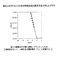
トランジスタの性能評価について図2、3を用いて説明する。 The transistor performance evaluation will be described with reference to FIGS.
このグラフは、後述の重合体Aと化合物aの混合試料を有機半導体層とする有機TFTに関するものである。 This graph relates to an organic TFT having a mixed sample of polymer A and compound a described later as an organic semiconductor layer.
有機半導体の電界効果移動度は、以下の式を用いて算出する。 The field effect mobility of the organic semiconductor is calculated using the following formula.
Ids=μCinW(Vg−Vth)2/2L
(ただし、Cinはゲート絶縁膜の単位面積あたりのキャパシタンス、Wはチャネル幅、L はチャネル長、Vgはゲート電圧、Idsはソース・ドレイン電流、μは移動度、Vth はチャネルが形成し始めるゲートの閾値電圧である。)
具体的には、ソース・ドレイン間に−20Vを印加して、ゲート電圧を10から−20V挿引した時の、ソース・ドレイン電流を測定する。
I ds = μC in W (V g −V th ) 2 / 2L
(Where Cin is the capacitance per unit area of the gate insulating film, W is the channel width, L is the channel length, Vg is the gate voltage, Ids is the source / drain current, μ is the mobility, and Vth is the gate where the channel begins to form. Threshold voltage.)
Specifically, -20V is applied between the source and drain, and the source / drain current is measured when the gate voltage is subtracted from 10 to -20V.
上記条件で測定されたソース・ドレイン電流の平方根をゲート電圧に対しプロットして直線近似を行う。近似曲線においてソース・ドレイン電流の平方根が0Aになるゲート電圧値をVthと定義する(図3)。 The square root of the source / drain current measured under the above conditions is plotted against the gate voltage to perform linear approximation. The gate voltage value at which the square root of the source / drain current in the approximate curve becomes 0 A is defined as Vth (FIG. 3).
以下、本発明を実施例に基づいて具体的に説明する。 Hereinafter, the present invention will be specifically described based on examples.
合成例1(重合体1の合成) Synthesis Example 1 (Synthesis of Polymer 1)
元素分析値(計算値);C:84.25%(84.02%),H:8.20%(7.93%),N:2.33%(2.45%)。 Elemental analysis value (calculated value); C: 84.25% (84.02%), H: 8.20% (7.93%), N: 2.33% (2.45%).
示差走査熱量測定から求めたガラス転移温度は117℃であった。GPCにより測定したポリスチレン換算の数平均分子量は8500、重量平均分子量は20000であった。 The glass transition temperature determined from differential scanning calorimetry was 117 ° C. The number average molecular weight in terms of polystyrene measured by GPC was 8500, and the weight average molecular weight was 20000.
合成例2(重合体2の合成) Synthesis Example 2 (Synthesis of Polymer 2)
元素分析値(計算値);C:85.18%(85.55%),H:8.03%(7.63%),N:2.10%(2.08%)。 Elemental analysis value (calculated value); C: 85.18% (85.55%), H: 8.03% (7.63%), N: 2.10% (2.08%).
示差走査熱量測定から求めたガラス転移温度は133℃であった。GPCにより測定したポリスチレン換算の数平均分子量は39200、重量平均分子量は116000であった。 The glass transition temperature determined from differential scanning calorimetry was 133 ° C. The number average molecular weight in terms of polystyrene measured by GPC was 39200, and the weight average molecular weight was 116000.
合成例3(重合体3の合成) Synthesis Example 3 (Synthesis of Polymer 3)
元素分析値(計算値);C:85.33%(85.55%),H:7.86%(7.63%),N:2.30%(2.08%)。 Elemental analysis value (calculated value); C: 85.33% (85.55%), H: 7.86% (7.63%), N: 2.30% (2.08%).
示差走査熱量測定から求めたガラス転移温度は152℃であった。GPCにより測定したポリスチレン換算の数平均分子量は44400、重量平均分子量は118000であった。 The glass transition temperature determined from differential scanning calorimetry was 152 ° C. The number average molecular weight in terms of polystyrene measured by GPC was 44400, and the weight average molecular weight was 118,000.
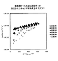
実施例1
下記重合体A(重量平均分子量109100、数平均分子量27100)90重量部および、下記化合物a10重量部からなる混合物の10wt%のテトラヒドロフラン溶液を調製した。この溶液をAl電極が蒸着されたPET基板上にブレード塗工し、120℃で30分乾燥して膜厚およそ10μmの薄膜を作製した。さらにこの半導体フィルム上に金を蒸着してサンドイッチセルを作製した。このセルを用いてタイムオブフライト法により有機半導体材料のキャリア移動度を測定した。結果を図4に示す。
Example 1
A 10 wt% tetrahydrofuran solution of a mixture comprising 90 parts by weight of the following polymer A (weight average molecular weight 109100, number average molecular weight 27100) and 10 parts by weight of the following compound a was prepared. This solution was blade-coated on a PET substrate on which an Al electrode was deposited, and dried at 120 ° C. for 30 minutes to produce a thin film having a thickness of about 10 μm. Further, gold was deposited on the semiconductor film to produce a sandwich cell. Using this cell, the carrier mobility of the organic semiconductor material was measured by the time-of-flight method. The results are shown in FIG.
重合体A80重量部、および化合物a20重量部からなる混合物を用いた以外は実施例1と同様の方法によりキャリア移動度を測定した。結果を図4に示す。
Carrier mobility was measured by the same method as in Example 1 except that a mixture consisting of 80 parts by weight of Polymer A and 20 parts by weight of Compound a was used. The results are shown in FIG.
実施例3
重合体A70重量部、および化合物a30重量部からなる混合物を用いた以外は実施例1と同様の方法によりキャリア移動度を測定した。結果を図4に示す。
Example 3
Carrier mobility was measured by the same method as in Example 1 except that a mixture consisting of 70 parts by weight of polymer A and 30 parts by weight of compound a was used. The results are shown in FIG.
実施例4
重合体A60重量部、および化合物a40重量部からなる混合物を用いた以外は実施例1と同様の方法によりキャリア移動度を測定した。結果を図4に示す。
Example 4
Carrier mobility was measured by the same method as in Example 1 except that a mixture consisting of 60 parts by weight of Polymer A and 40 parts by weight of Compound a was used. The results are shown in FIG.
実施例5
重合体A50重量部、および化合物a50重量部からなる混合物を用いた以外は実施例1と同様の方法によりキャリア移動度を測定した。結果を図4に示す。
Example 5
Carrier mobility was measured by the same method as in Example 1 except that a mixture consisting of 50 parts by weight of Polymer A and 50 parts by weight of Compound a was used. The results are shown in FIG.
比較例1
重合体Aのみの10wt%のテトラヒドロフラン溶液を用いた以外は実施例1と同様の方法によりキャリア移動度を測定した。結果を図4に示す。
Comparative Example 1
Carrier mobility was measured by the same method as in Example 1 except that a 10 wt% tetrahydrofuran solution containing only polymer A was used. The results are shown in FIG.
図4から明らかなように、重合体Aと化合物aの混合試料(実施例1〜5)は、何れも重合体Aのみ(比較例1)の試料と比較して、何れの電界強度においても高速なキャリア移動度を示した。また化合物aのみの試料では、重合体Aよりも低い値であり、本発明における両材料の混合により好特性が得られることが示された。 As is clear from FIG. 4, the mixed samples of polymer A and compound a (Examples 1 to 5) are all in any electric field strength as compared with the sample of only polymer A (Comparative Example 1). Fast carrier mobility was shown. In addition, the sample containing only the compound a has a lower value than that of the polymer A, and it was shown that good characteristics can be obtained by mixing both materials in the present invention.
実施例6
重合体Aおよび化合物aの混合材料を用いて図1(A)に示される構造の薄膜デバイスを作製した。p−ドープされてゲートとして作用するシリコン基板表面を熱酸化してSiO2の絶縁層を50nm形成した後、酸化膜を片面だけ除去し、除去した面にAlを蒸着してゲート電極とした。次に該SiO2の絶縁層上にチャネル長40μm、チャネル幅10mmとなるようにソース電極およびドレイン電極のAu/Cr膜を蒸着した。引き続き、重合体Aおよび化合物aの混合材料(重合体Aを60重量部、化合物aを40重量部)の1.0wt%のトルエン溶液をスピンコートして乾燥することにより膜厚約20nm有機半導体層を作製した。
Example 6
A thin film device having a structure shown in FIG. 1A was manufactured using a mixed material of the polymer A and the compound a. A p-doped silicon substrate surface acting as a gate was thermally oxidized to form an SiO 2 insulating layer having a thickness of 50 nm, and then only one side of the oxide film was removed, and Al was evaporated on the removed surface to form a gate electrode. Next, an Au / Cr film of a source electrode and a drain electrode was deposited on the SiO 2 insulating layer so as to have a channel length of 40 μm and a channel width of 10 mm. Subsequently, a 1.0 wt% toluene solution of a mixed material of polymer A and compound a (60 parts by weight of polymer A and 40 parts by weight of compound a) is spin-coated and dried to form an organic semiconductor having a thickness of about 20 nm. A layer was made.
このようにして作製した有機TFTのトランジスタ特性を図5に示す。図5から明らかなように、作製したデバイスは良好なトランジスタ特性を示した。 The transistor characteristics of the organic TFT thus fabricated are shown in FIG. As is apparent from FIG. 5, the fabricated device showed good transistor characteristics.
また、下記の式を用いて有機半導体の電界効果移動度を算出した。 Moreover, the field effect mobility of the organic semiconductor was computed using the following formula.
Ids=μCinW(Vg−Vth)2/2L
(ただし、Cinはゲート絶縁膜の単位面積あたりのキャパシタンス、Wはチャネル幅、Lはチャネル長、Vgはゲート電圧、Idsはソースドレイン電流、μは移動度、Vthはチャネルが形成し始めるゲートのしきい値電圧である。)
作製したTFTの移動度は3.01×10⁻³(cm2/Vsec)の高移動度であった。
I ds = μC in W (V g −V th ) 2 / 2L
(Where C in is the capacitance per unit area of the gate insulating film, W is the channel width, L is the channel length, V g is the gate voltage, I ds is the source drain current, μ is the mobility, and V th is the channel. (This is the threshold voltage of the gate that starts.)
The mobility of the fabricated TFT was a high mobility of 3.01 × 10 −3 (cm 2 / Vsec).
またオンオフ比(Vg=−20VでVds=−20Vの場合に観測されたIdsとVg=0VでVds=−20Vの場合に観測されたIdsの比)は2.6×10⁴であり、優れた値であった。以上のように、作製した有機TFTは優れた特性を示した。 The (ratio of the observed I ds when in the observed I ds and V g = 0V in the case of V ds = -20 V in V g = -20 V of V ds = -20 V) off ratio is 2.6 × It was 10 4 and was an excellent value. As described above, the produced organic TFT showed excellent characteristics.
また環境性評価、即ちこの素子の(1)作製直後の電気特性評価、及び、(2)1週間大気中に放置後の電気特性評価を行った。(1)における値と、(2)における値の比(2)/(1)を取り、この値を変動比として評価した。その結果、オン電流の変化率は1.00、また、オンオフ比の変化率は1.00であり耐環境性に優れていた。 In addition, environmental evaluation, that is, (1) evaluation of electrical characteristics immediately after fabrication of the device, and (2) evaluation of electrical characteristics after being left in the atmosphere for one week. The ratio (2) / (1) between the value in (1) and the value in (2) was taken, and this value was evaluated as the fluctuation ratio. As a result, the change rate of the on-current was 1.00, and the change rate of the on-off ratio was 1.00, which was excellent in environmental resistance.
実施例7
重合体Aおよび化合物aの混合材料を用いて図1(B)に示される構造の薄膜デバイスを作製した。p−ドープされてゲートとして作用するシリコン基板表面を熱酸化してSiO2の絶縁層を50nm形成した後、酸化膜を片面だけ除去し、除去した面にAlを蒸着してゲート電極とした。次に該SiO2の絶縁層上に、重合体Aおよび化合物aの混合材料(重合体Aを60重量部、化合物aを40重量部)の1.0wt%のトルエン溶液をスピンコートして乾燥することにより膜厚約20nmの有機半導体層を作製した。乾燥した後、有機半導体層上にチャネル長40μm、チャネル幅10mmのソース・ドレイン電極のAuを蒸着した。
Example 7
A thin film device having a structure shown in FIG. 1B was manufactured using a mixed material of the polymer A and the compound a. A p-doped silicon substrate surface acting as a gate was thermally oxidized to form an SiO 2 insulating layer having a thickness of 50 nm, and then only one side of the oxide film was removed, and Al was evaporated on the removed surface to form a gate electrode. Next, a 1.0 wt% toluene solution of a mixed material of polymer A and compound a (60 parts by weight of polymer A and 40 parts by weight of compound a) is spin-coated on the insulating layer of SiO 2 and dried. As a result, an organic semiconductor layer having a thickness of about 20 nm was produced. After drying, Au of a source / drain electrode having a channel length of 40 μm and a channel width of 10 mm was deposited on the organic semiconductor layer.
このようにして作製した有機TFTのトランジスタ特性を測定したところ、実施例6とほぼ同じ結果であり、作製した有機TFTはキャリア移動度、オンオフ比、耐環境性に優れた特性を示した。 The transistor characteristics of the organic TFT produced in this manner were measured. The results were almost the same as in Example 6. The produced organic TFT showed excellent carrier mobility, on / off ratio, and environmental resistance.
比較例2
有機半導体層として重合体Aのみを用いた以外は実施例6と同様の方法により、図1(A)に示される構造の薄膜デバイスを作製した。作製した有機TFTのトランジスタ特性を図6に示す。作製した有機TFTにおける移動度は1.20×10⁻⁴(cm2/Vsec)であった。またオンオフ比は1.5×103であり、実施例6、7には劣る性能であった。
Comparative Example 2
A thin film device having the structure shown in FIG. 1A was produced in the same manner as in Example 6 except that only the polymer A was used as the organic semiconductor layer. The transistor characteristics of the produced organic TFT are shown in FIG. The mobility in the produced organic TFT was 1.20 × 10 −4 (cm 2 / Vsec). The on / off ratio was 1.5 × 10 3 , which was inferior to Examples 6 and 7.
比較例3
有機半導体層としてポリ−3−ヘキシルチオフェンを用いた以外は実施例7と同様の方法により、図1(B)に示される構造の薄膜デバイスを作製した。作製した有機TFTにおける移動度は7.76×10⁻⁵(cm2/Vsec)であった。また、オフ電流(Vg=0Vの場合のIds)が大きい為に、オンオフ比は10程度であった。この素子の耐環境性評価を実施例6と同様に実施した。その結果オン電流の変化率は0.80、またオンオフ比の変化率は0.62であり、移動度、オンオフ比、耐環境性ともに本発明に劣る結果であった。
Comparative Example 3
A thin film device having the structure shown in FIG. 1B was fabricated in the same manner as in Example 7 except that poly-3-hexylthiophene was used as the organic semiconductor layer. The mobility of the produced organic TFT was 7.76 × 10 −5 (cm 2 / Vsec). Further, since the off current (I ds when V g = 0V) is large, the on / off ratio was about 10. The environmental resistance of this device was evaluated in the same manner as in Example 6. As a result, the change rate of the on-current was 0.80 and the change rate of the on-off ratio was 0.62, and the mobility, on-off ratio, and environmental resistance were inferior to those of the present invention.
実施例8
重合体Aおよび化合物aの混合材料を用いて図1(B)に示される構造の薄膜デバイスを作製した。p−ドープされてゲートとして作用するシリコン基板表面を熱酸化してSiO2の絶縁層を50nm形成した後、酸化膜を片面だけ除去し、除去した面にAlを蒸着してゲート電極とした。次に該SiO2の絶縁層上に、重合体Aおよび化合物aの混合材料(重合体Aを60重量部、化合物aを40重量部)の1.0wt%のTHF/pキシレン(80/20)混合溶液にて塗布液を調整し、スピンコートして乾燥することにより膜厚30nmの有機半導体層を作製した。乾燥した後、有機半導体層上にチャネル長40μm、チャネル幅10mmのソース・ドレイン電極のAuを蒸着した。
Example 8
A thin film device having a structure shown in FIG. 1B was manufactured using a mixed material of the polymer A and the compound a. A p-doped silicon substrate surface acting as a gate was thermally oxidized to form an SiO 2 insulating layer having a thickness of 50 nm, and then only one side of the oxide film was removed, and Al was evaporated on the removed surface to form a gate electrode. Next to the SiO 2 insulating layer, the mixed material (polymer A 60 parts by weight, the compound a 40 parts by weight) of the polymer A and the compound a 1.0 wt% of THF / p-xylene (80/20 ) A coating solution was prepared with a mixed solution, spin-coated and dried to prepare an organic semiconductor layer having a thickness of 30 nm. After drying, Au of a source / drain electrode having a channel length of 40 μm and a channel width of 10 mm was deposited on the organic semiconductor layer.
また、下記の式を用いて有機半導体の電界効果移動度を算出した。 Moreover, the field effect mobility of the organic semiconductor was computed using the following formula.
Ids=μCinW(Vg−Vth)2/2L
(ただし、Cin、W、L、Vg、Ids、μ、Vthは実施例6において定義したものと同じである。)
作製したTFTはデプレッションモードで動作し、移動度は1.04×10⁻³(cm2/Vs)の高移動度であった。
I ds = μC in W (V g −V th ) 2 / 2L
(However, Cin, W, L, Vg, Ids, μ, and Vth are the same as those defined in Example 6.)
The manufactured TFT operated in a depletion mode, and the mobility was as high as 1.04 × 10 −3 (cm 2 / Vs).
また環境性評価、即ちこの素子の(1)作製直後の電気特性評価、及び、(2)1週間大気中に放置後の電気特性評価を行った。(1)における値と、(2)における値の比(2)/(1)を取り、この値を変動比として評価した。その結果、オン電流の変化率は1.00、また、オンオフ比の変化率は1.00であり耐環境性に優れていた。 In addition, environmental evaluation, that is, (1) evaluation of electrical characteristics immediately after fabrication of the device, and (2) evaluation of electrical characteristics after being left in the atmosphere for one week. The ratio (2) / (1) between the value in (1) and the value in (2) was taken, and this value was evaluated as the fluctuation ratio. As a result, the change rate of the on-current was 1.00, and the change rate of the on-off ratio was 1.00, which was excellent in environmental resistance.
実施例9
重合体Aおよび化合物aの混合材料を用いて図1(A)に示される構造の薄膜デバイスを作製した。p−ドープされてゲートとして作用するシリコン基板表面を熱酸化してSiO2の絶縁層を50nm形成した後、酸化膜を片面だけ除去し、除去した面にAlを蒸着してゲート電極とした。次に該SiO2の絶縁層上にチャネル長40μm、チャネル幅10mmとなるようにソース電極およびドレイン電極のAu/Cr膜を蒸着した。引き続き、重合体Aおよび化合物aの混合材料(重合体Aを60重量部、化合物aを40重量部)の1.0wt%のTHF/pキシレン(80/20)混合溶液にて塗布液を調整し、スピンコートして乾燥することにより膜厚30nm有機半導体層を作製した。
Example 9
A thin film device having a structure shown in FIG. 1A was manufactured using a mixed material of the polymer A and the compound a. A p-doped silicon substrate surface acting as a gate was thermally oxidized to form an SiO 2 insulating layer having a thickness of 50 nm, and then only one side of the oxide film was removed, and Al was evaporated on the removed surface to form a gate electrode. Next, an Au / Cr film of a source electrode and a drain electrode was deposited on the SiO 2 insulating layer so as to have a channel length of 40 μm and a channel width of 10 mm. Subsequently, the coating solution was adjusted with a 1.0 wt% THF / p-xylene (80/20) mixed solution of a mixed material of polymer A and compound a (60 parts by weight of polymer A and 40 parts by weight of compound a). Then, an organic semiconductor layer having a thickness of 30 nm was produced by spin coating and drying.
このようにして作製した有機TFTのトランジスタ特性を測定したところ、実施例8とほぼ同じ結果であり、作製した有機TFTはキャリア移動度、オンオフ比、耐環境性に優れた特性を示した。 The transistor characteristics of the organic TFT produced in this way were measured. The results were almost the same as in Example 8. The produced organic TFT showed excellent characteristics in carrier mobility, on / off ratio, and environmental resistance.
比較例4
有機半導体層として重合体Aのみを用いた以外は実施例8と同様の方法により、有機TFTを作製した。作製した有機TFTにおける移動度は2.70×10⁻⁵(cm2/Vs)であり、実施例8、9には劣る性能であった。
Comparative Example 4
An organic TFT was produced in the same manner as in Example 8 except that only the polymer A was used as the organic semiconductor layer. The mobility in the produced organic TFT was 2.70 × 10 −5 (cm 2 / Vs), which was inferior to Examples 8 and 9.
有機半導体層としてポリ−3−ヘキシルチオフェンを用いた以外は実施例9と同様の方法により、図1(A)に示される構造の薄膜デバイスを作製した。作製した有機TFTにおける移動度は7.76×10⁻⁵(cm2/Vs)であった。また、オフ電流(Vg=0Vの場合のIds)が大きい為に、オンオフ比は10程度であった。この素子の耐環境性評価を実施例6と同様に実施した。その結果オン電流の変化率は0.80、またオンオフ比の変化率は0.62であり、移動度、オンオフ比、耐環境性ともに本発明のものに比較して劣る結果であった。 A thin film device having the structure shown in FIG. 1A was produced in the same manner as in Example 9 except that poly-3-hexylthiophene was used as the organic semiconductor layer. The mobility of the produced organic TFT was 7.76 × 10 −5 (cm 2 / Vs). Further, since the off current (I ds when V g = 0V) is large, the on / off ratio was about 10. The environmental resistance of this device was evaluated in the same manner as in Example 6. As a result, the change rate of the on-current was 0.80, and the change rate of the on-off ratio was 0.62, which was inferior to that of the present invention in terms of mobility, on-off ratio, and environmental resistance.
実施例10
ゲート絶縁膜をHMDS処理し、重合体Aおよび化合物aの混合材料を用いて実施例8記載の方法でTFTを作製した。ただし、有機半導体溶液はトルエン80%、パラキシレン20%使用した。
Example 10
The gate insulating film was treated with HMDS, and a TFT was fabricated by the method described in Example 8 using a mixed material of polymer A and compound a. However, the organic semiconductor solution was 80% toluene and 20% paraxylene.
このようにして作製した有機TFTはエンハンスメントモードで動作した。これはトランジスタ駆動上、大変好適になる(結果は図2)。移動度は3.01×10⁻³(cm2/Vs)であった。 The organic TFT thus fabricated operated in the enhancement mode. This is very suitable for transistor driving (result is FIG. 2). The mobility was 3.01 × 10 −3 (cm 2 / Vs).
HMDS処理時間、その後の熱処理温度を変化させ、さらにオクタドデシルトリクロロシランなどの表面改質剤を用いて、表面エネルキーの適正範囲を検討した。 The appropriate range of surface energy was examined by changing the HMDS treatment time and the subsequent heat treatment temperature, and further using a surface modifier such as octadodecyltrichlorosilane.
表面エネルギーはジスマンプロットから求め、標準試験溶液として、水、グリセリン、ホルムアミド、ジエチレングリコール、ジプロピレングリコールを用いて評価した。表面エネルギーが25mN/mより低い場合、スピンコーティングによる成膜が出来ず(塗布液がはじかれる)、40mN/mを超える場合では、閾値電圧は正(デプレッションモード)で好ましくなく、良好な結果を与える表面エネルギーは25mN/m以上、40mN/m以下の範囲であった。 The surface energy was determined from the Dysman plot and evaluated using water, glycerin, formamide, diethylene glycol, and dipropylene glycol as standard test solutions. When the surface energy is lower than 25 mN / m, film formation by spin coating cannot be performed (the coating solution is repelled). When the surface energy exceeds 40 mN / m, the threshold voltage is positive (depletion mode), which is not preferable. The surface energy applied was in the range of 25 mN / m or more and 40 mN / m or less.
Claims (17)
Aは下記一般式(1)、(2)で示される基、9−アントリル基または置換もしくは無置換のカルバゾリル基を表す。
A represents a group represented by the following general formulas (1) and (2), a 9-anthryl group, or a substituted or unsubstituted carbazolyl group.
Priority Applications (3)
| Application Number | Priority Date | Filing Date | Title |
|---|---|---|---|
| JP2004024878A JP4480410B2 (en) | 2003-10-31 | 2004-01-30 | Organic semiconductor material, organic thin film transistor, and manufacturing method thereof |
| US10/777,095 US7166689B2 (en) | 2003-02-13 | 2004-02-13 | Aryl amine polymer, thin film transistor using the aryl amine polymer, and method of manufacturing the thin film transistor |
| US11/566,728 US7550554B2 (en) | 2003-02-13 | 2006-12-05 | Aryl amine polymer, thin film transistor using the new aryl amine polymer, and method of manufacturing the thin film transistor |
Applications Claiming Priority (2)
| Application Number | Priority Date | Filing Date | Title |
|---|---|---|---|
| JP2003373723 | 2003-10-31 | ||
| JP2004024878A JP4480410B2 (en) | 2003-10-31 | 2004-01-30 | Organic semiconductor material, organic thin film transistor, and manufacturing method thereof |
Publications (3)
| Publication Number | Publication Date |
|---|---|
| JP2005154709A JP2005154709A (en) | 2005-06-16 |
| JP2005154709A5 JP2005154709A5 (en) | 2007-03-08 |
| JP4480410B2 true JP4480410B2 (en) | 2010-06-16 |
Family
ID=34741328
Family Applications (1)
| Application Number | Title | Priority Date | Filing Date |
|---|---|---|---|
| JP2004024878A Expired - Lifetime JP4480410B2 (en) | 2003-02-13 | 2004-01-30 | Organic semiconductor material, organic thin film transistor, and manufacturing method thereof |
Country Status (1)
| Country | Link |
|---|---|
| JP (1) | JP4480410B2 (en) |
Families Citing this family (8)
| Publication number | Priority date | Publication date | Assignee | Title |
|---|---|---|---|---|
| JP2006228935A (en) * | 2005-02-17 | 2006-08-31 | Ricoh Co Ltd | Organic thin film transistor |
| WO2007026608A1 (en) * | 2005-08-31 | 2007-03-08 | Riken | Organic thin film transistor, and method for surface modification of gate insulating layer in organic thin film transistor |
| JP2007077223A (en) * | 2005-09-13 | 2007-03-29 | Ricoh Co Ltd | Poly(triarylamine) |
| JP2007123580A (en) * | 2005-10-28 | 2007-05-17 | Konica Minolta Holdings Inc | Method of forming organic semiconductor film and organic thin film semiconductor |
| JP2007123620A (en) * | 2005-10-28 | 2007-05-17 | Ricoh Co Ltd | Organic semiconductor device and method of manufacturing same, and active matrix display device |
| WO2007129832A1 (en) * | 2006-05-04 | 2007-11-15 | Lg Chem, Ltd. | Composition for forming gate insulating layer of organic thin-film transistor and organic thin film transistor using the same |
| JP5205763B2 (en) | 2006-09-19 | 2013-06-05 | 株式会社リコー | Organic thin film transistor |
| JP5729540B2 (en) * | 2010-12-16 | 2015-06-03 | 株式会社リコー | Field effect transistor and manufacturing method thereof |
-
2004
- 2004-01-30 JP JP2004024878A patent/JP4480410B2/en not_active Expired - Lifetime
Also Published As
| Publication number | Publication date |
|---|---|
| JP2005154709A (en) | 2005-06-16 |
Similar Documents
| Publication | Publication Date | Title |
|---|---|---|
| US7550554B2 (en) | Aryl amine polymer, thin film transistor using the new aryl amine polymer, and method of manufacturing the thin film transistor | |
| TWI296157B (en) | Organic thin film transistor | |
| JP5220005B2 (en) | Thiazolothiazole derivatives and organic electronic devices using the same | |
| KR20120043009A (en) | Novel organic semiconductive material and electronic device using the same | |
| JP5025074B2 (en) | Organic thin film transistor and method for producing organic thin film transistor | |
| TWI549327B (en) | Organic field effect transistor and organic semiconductor material | |
| JP2008078653A (en) | Organic thin film transistor comprising phosphate ester based self-organized monomolecular film, and method of manufacturing the same | |
| TW200929651A (en) | Thin film transistors | |
| JP2006319102A (en) | Light emitting element | |
| TW200926418A (en) | Thin film transistors | |
| JP4480410B2 (en) | Organic semiconductor material, organic thin film transistor, and manufacturing method thereof | |
| KR100790928B1 (en) | Arylamine polymer and organic thin film transistor having an organic semiconductor layer containing the arylamine polymer | |
| JP2006232898A (en) | Electroconductive polymer material, field-effect transistor using the same and method for producing the same | |
| JP5096731B2 (en) | Novel aromatic enediyne derivative, precursor solution for producing organic semiconductor containing the same, organic semiconductor thin film using the precursor solution, method for producing the same, and electronic device | |
| JP4891552B2 (en) | Organic thin film transistor and manufacturing method thereof | |
| JP2010225974A (en) | Organic semiconductor composite and organic field effect transistor using the same | |
| JP4942943B2 (en) | Organic semiconductor material, field effect transistor using the same, and manufacturing method thereof | |
| JP5105938B2 (en) | Polymer and process for producing the same | |
| JP5218812B2 (en) | Organic thin film transistor | |
| JP5030444B2 (en) | Organic thin film transistor | |
| JP5403578B2 (en) | Organic semiconductor thin film and organic thin film transistor using the same | |
| JP4922563B2 (en) | Organic thin film transistor | |
| JP2008227339A (en) | Organic thin film transistor | |
| JP5063053B2 (en) | Organic thin film transistor | |
| JP5032781B2 (en) | Organic thin film transistor |
Legal Events
| Date | Code | Title | Description |
|---|---|---|---|
| A521 | Request for written amendment filed |
Free format text: JAPANESE INTERMEDIATE CODE: A523 Effective date: 20070124 |
|
| A621 | Written request for application examination |
Free format text: JAPANESE INTERMEDIATE CODE: A621 Effective date: 20070124 |
|
| A977 | Report on retrieval |
Free format text: JAPANESE INTERMEDIATE CODE: A971007 Effective date: 20100222 |
|
| TRDD | Decision of grant or rejection written | ||
| A01 | Written decision to grant a patent or to grant a registration (utility model) |
Free format text: JAPANESE INTERMEDIATE CODE: A01 Effective date: 20100309 |
|
| A01 | Written decision to grant a patent or to grant a registration (utility model) |
Free format text: JAPANESE INTERMEDIATE CODE: A01 |
|
| A61 | First payment of annual fees (during grant procedure) |
Free format text: JAPANESE INTERMEDIATE CODE: A61 Effective date: 20100316 |
|
| FPAY | Renewal fee payment (event date is renewal date of database) |
Free format text: PAYMENT UNTIL: 20130326 Year of fee payment: 3 |
|
| R150 | Certificate of patent or registration of utility model |
Ref document number: 4480410 Country of ref document: JP Free format text: JAPANESE INTERMEDIATE CODE: R150 Free format text: JAPANESE INTERMEDIATE CODE: R150 |
|
| FPAY | Renewal fee payment (event date is renewal date of database) |
Free format text: PAYMENT UNTIL: 20140326 Year of fee payment: 4 |
|
| R250 | Receipt of annual fees |
Free format text: JAPANESE INTERMEDIATE CODE: R250 |