JP4460741B2 - Power semiconductor device and manufacturing method thereof - Google Patents
Power semiconductor device and manufacturing method thereof Download PDFInfo
- Publication number
- JP4460741B2 JP4460741B2 JP2000294316A JP2000294316A JP4460741B2 JP 4460741 B2 JP4460741 B2 JP 4460741B2 JP 2000294316 A JP2000294316 A JP 2000294316A JP 2000294316 A JP2000294316 A JP 2000294316A JP 4460741 B2 JP4460741 B2 JP 4460741B2
- Authority
- JP
- Japan
- Prior art keywords
- base layer
- type base
- conductivity type
- layer
- power semiconductor
- Prior art date
- Legal status (The legal status is an assumption and is not a legal conclusion. Google has not performed a legal analysis and makes no representation as to the accuracy of the status listed.)
- Expired - Fee Related
Links
- 239000004065 semiconductor Substances 0.000 title claims description 58
- 238000004519 manufacturing process Methods 0.000 title claims description 21
- 238000000034 method Methods 0.000 claims description 9
- 239000010410 layer Substances 0.000 description 253
- 239000012535 impurity Substances 0.000 description 20
- 238000009826 distribution Methods 0.000 description 12
- 238000009413 insulation Methods 0.000 description 8
- 239000011229 interlayer Substances 0.000 description 6
- 230000007423 decrease Effects 0.000 description 5
- 238000013459 approach Methods 0.000 description 4
- 238000010586 diagram Methods 0.000 description 4
- 238000002347 injection Methods 0.000 description 4
- 239000007924 injection Substances 0.000 description 4
- 230000003068 static effect Effects 0.000 description 4
- 230000015556 catabolic process Effects 0.000 description 3
- 239000000463 material Substances 0.000 description 3
- 229920006395 saturated elastomer Polymers 0.000 description 3
- VYPSYNLAJGMNEJ-UHFFFAOYSA-N Silicium dioxide Chemical compound O=[Si]=O VYPSYNLAJGMNEJ-UHFFFAOYSA-N 0.000 description 2
- 238000009792 diffusion process Methods 0.000 description 2
- 238000002513 implantation Methods 0.000 description 2
- 239000000758 substrate Substances 0.000 description 2
- 101100379079 Emericella variicolor andA gene Proteins 0.000 description 1
- 229910052581 Si3N4 Inorganic materials 0.000 description 1
- 229910004298 SiO 2 Inorganic materials 0.000 description 1
- 238000006243 chemical reaction Methods 0.000 description 1
- 230000006378 damage Effects 0.000 description 1
- 230000000694 effects Effects 0.000 description 1
- BPUBBGLMJRNUCC-UHFFFAOYSA-N oxygen(2-);tantalum(5+) Chemical compound [O-2].[O-2].[O-2].[O-2].[O-2].[Ta+5].[Ta+5] BPUBBGLMJRNUCC-UHFFFAOYSA-N 0.000 description 1
- 235000012239 silicon dioxide Nutrition 0.000 description 1
- 239000000377 silicon dioxide Substances 0.000 description 1
- HQVNEWCFYHHQES-UHFFFAOYSA-N silicon nitride Chemical compound N12[Si]34N5[Si]62N3[Si]51N64 HQVNEWCFYHHQES-UHFFFAOYSA-N 0.000 description 1
- 238000004088 simulation Methods 0.000 description 1
- PBCFLUZVCVVTBY-UHFFFAOYSA-N tantalum pentoxide Inorganic materials O=[Ta](=O)O[Ta](=O)=O PBCFLUZVCVVTBY-UHFFFAOYSA-N 0.000 description 1
Images


Classifications
-
- H—ELECTRICITY
- H01—ELECTRIC ELEMENTS
- H01L—SEMICONDUCTOR DEVICES NOT COVERED BY CLASS H10
- H01L29/00—Semiconductor devices adapted for rectifying, amplifying, oscillating or switching, or capacitors or resistors with at least one potential-jump barrier or surface barrier, e.g. PN junction depletion layer or carrier concentration layer; Details of semiconductor bodies or of electrodes thereof ; Multistep manufacturing processes therefor
- H01L29/66—Types of semiconductor device ; Multistep manufacturing processes therefor
- H01L29/68—Types of semiconductor device ; Multistep manufacturing processes therefor controllable by only the electric current supplied, or only the electric potential applied, to an electrode which does not carry the current to be rectified, amplified or switched
- H01L29/76—Unipolar devices, e.g. field effect transistors
- H01L29/772—Field effect transistors
- H01L29/78—Field effect transistors with field effect produced by an insulated gate
- H01L29/7801—DMOS transistors, i.e. MISFETs with a channel accommodating body or base region adjoining a drain drift region
- H01L29/7802—Vertical DMOS transistors, i.e. VDMOS transistors
-
- H—ELECTRICITY
- H01—ELECTRIC ELEMENTS
- H01L—SEMICONDUCTOR DEVICES NOT COVERED BY CLASS H10
- H01L29/00—Semiconductor devices adapted for rectifying, amplifying, oscillating or switching, or capacitors or resistors with at least one potential-jump barrier or surface barrier, e.g. PN junction depletion layer or carrier concentration layer; Details of semiconductor bodies or of electrodes thereof ; Multistep manufacturing processes therefor
- H01L29/40—Electrodes ; Multistep manufacturing processes therefor
- H01L29/41—Electrodes ; Multistep manufacturing processes therefor characterised by their shape, relative sizes or dispositions
- H01L29/423—Electrodes ; Multistep manufacturing processes therefor characterised by their shape, relative sizes or dispositions not carrying the current to be rectified, amplified or switched
- H01L29/42312—Gate electrodes for field effect devices
- H01L29/42316—Gate electrodes for field effect devices for field-effect transistors
- H01L29/4232—Gate electrodes for field effect devices for field-effect transistors with insulated gate
- H01L29/42364—Gate electrodes for field effect devices for field-effect transistors with insulated gate characterised by the insulating layer, e.g. thickness or uniformity
- H01L29/42368—Gate electrodes for field effect devices for field-effect transistors with insulated gate characterised by the insulating layer, e.g. thickness or uniformity the thickness being non-uniform
-
- H—ELECTRICITY
- H01—ELECTRIC ELEMENTS
- H01L—SEMICONDUCTOR DEVICES NOT COVERED BY CLASS H10
- H01L29/00—Semiconductor devices adapted for rectifying, amplifying, oscillating or switching, or capacitors or resistors with at least one potential-jump barrier or surface barrier, e.g. PN junction depletion layer or carrier concentration layer; Details of semiconductor bodies or of electrodes thereof ; Multistep manufacturing processes therefor
- H01L29/66—Types of semiconductor device ; Multistep manufacturing processes therefor
- H01L29/68—Types of semiconductor device ; Multistep manufacturing processes therefor controllable by only the electric current supplied, or only the electric potential applied, to an electrode which does not carry the current to be rectified, amplified or switched
- H01L29/70—Bipolar devices
- H01L29/72—Transistor-type devices, i.e. able to continuously respond to applied control signals
- H01L29/739—Transistor-type devices, i.e. able to continuously respond to applied control signals controlled by field-effect, e.g. bipolar static induction transistors [BSIT]
- H01L29/7393—Insulated gate bipolar mode transistors, i.e. IGBT; IGT; COMFET
- H01L29/7395—Vertical transistors, e.g. vertical IGBT
- H01L29/7396—Vertical transistors, e.g. vertical IGBT with a non planar surface, e.g. with a non planar gate or with a trench or recess or pillar in the surface of the emitter, base or collector region for improving current density or short circuiting the emitter and base regions
- H01L29/7397—Vertical transistors, e.g. vertical IGBT with a non planar surface, e.g. with a non planar gate or with a trench or recess or pillar in the surface of the emitter, base or collector region for improving current density or short circuiting the emitter and base regions and a gate structure lying on a slanted or vertical surface or formed in a groove, e.g. trench gate IGBT
Description
【0001】
【発明の属する技術分野】
本発明は、インバータなど電力変換装置を構成する電力半導体素子のなかで、IGBT、パワーMOSFETに係り、特に負荷短絡耐量を向上させた素子構造に関する。
【0002】
【従来の技術】
近年のパワーエレクトロニクス分野における電源機器の小型化、高性能化への要求を受けて、電力用半導体素子では、高耐圧化、大電流化と共に、低損失化、高破壊耐量化、高速化に対する性能改善が注力されている。特に高耐圧化、高電流化という点で、300V程度以上の耐圧を有する電力用半導体素子としてパワーMOSFETよりも低オン電圧を得ることができるIGBTが用いられている。
【0003】
この種のIGBTとしては、ゲートを平板状に設けたプレーナ構造およびゲートを構内に埋め込み形成したトレンチ構造の2種類が広く知られている。
【0004】
図11は、この種のプレーナ構造を有するIGBTの構成を示す断面図である。このIGBTでは、高抵抗のn型ベース層101の表面に高濃度のp型コレクタ層102が形成され、他方の面には、選択的にp型ベース層106が形成され、さらに、p型ベース層106内には、n型エミッタ層107が選択的に形成されている。
【0005】
n型ベース層101上とp型ベース層106上の一部およびn型エミッタ層107上の一部にゲート酸化膜103が設けられている。また、エミッタ電極109が、p型ベース層106とn型エミッタ層107に設けられる。ゲート電極105は、ゲート酸化膜103と層間絶縁膜104によってエミッタ電極109およびn型ベース層101およびp型ベース層106と絶縁されている。
【0006】
n型ベース層101、p型ベース層106、n型エミッタ層107、ゲート電極105によって、CHをチャネル領域とする電子注入用MOSFETが構成されている。さらに、n型エミッタ層107とp型ベース層106上には両方に接するようにエミッタ電極109が設けられている。
【0007】
上記構造において従来のプレーナ構造のIGBTでは、n型エミッタ層107とp型ベース層106は、それぞれ不純物の注入および熱拡散によって形成されるために、それらの不純物分布はガウス分布に準じる分布となることから、チャネル領域CHに沿った不純物濃度分布をみるとn型エミッタ層107とp型ベース層106との接合付近にp型不純物濃度の最高値があり、p型ベース層106とn型ベース層101の接合付近に近づくほど徐々にp型不純物濃度が下がっていく。
【0008】
次にIGBTの動作を説明する。プレーナ構造のIGBTとトレンチ構造のIGBTは、動作原理は同様であるので以下では、プレーナ構造のIGBTの動作を説明する。
【0009】
コレクタ電極108に正電圧、エミッタ電極109に負電圧が印加されているとき、エミッタ電極109より正となる正電圧をゲート電極105に印加すると、p型ベース層106のゲート電極105に接した表面がn型に反転し、電子eがn型エミッタ層107から反転層を介してn型ベース層101に注入されてp型コレクタ層102に達する。これによってn型ベース層101とp型コレクタ層102が順バイアスされて、p型コレクタ層102から正孔hがn型ベース層101に注入される。このように、n型ベース層101に電子eと正孔hの両方が注入され、n型ベース層101領域で電導率変調が起こってオン電圧が低減される。すなわち、素子が導通状態になる。
【0010】
一方、ターンオフするには、ゲート電極105にエミッタ電極109に対して負の電圧が印加される。これにより、ゲート電極105に接したp型ベース層106の表面に形成されていた反転層が消失して、電子注入が停止する。一方、n型ベース層101内に蓄積されていた正孔hは、その一部がp型ベース層106を介してエミッタ電極109に排出され、残りの正孔hが電子eと再結合して消滅し、素子はターンオフする。
【0011】
ここで素子が負荷短絡状態になった場合、素子は導通状態でコレクタ電極108に電源電圧が印加される。これによって素子には大きな短絡ピーク電流(Icp)が流れ、ある一定時間(tsc)で素子は破壊する。従来のIGBTでは、チャネル密度を大きくするとオン電圧を低減することができたが、一方でチャネル密度の増加は電流を流し易くなる結果、短絡ピーク電流(Icp)を大きくし負荷短絡耐量(tsc)が小さくなるという問題があった。
【0012】
【発明が解決しようとする課題】
以上述べたように、従来の半導体素子では、負荷短絡耐量が小さいという問題がある。
【0013】
本発明は上記事情を考慮してなされたもので、低いオン電圧を維持しつつ高い負荷短絡耐量を同時に実現し得る電力用半導体素子及びその製造方法を提供することにある。
【0014】
【課題を解決するための手段】
上記の目的を達成するために、本発明の第1の態様は、電力用半導体素子であって、第1導電型ベース層と、前記第1導電型ベース層の一方の表面に選択的に形成された第2導電型ベース層と、前記第2導電型ベース層の表面に選択的に形成された第1導電型エミッタ層と、前記第1導電型ベース層の一方及び他方の表面の1つに選択的に形成されたコレクタ層と、前記コレクタ層上に形成された第1の主電極と、前記第1導電型エミッタ層上及び前記第2導電型ベース層上に形成された第2の主電極と、第1絶縁部と第2絶縁部とを含み、前記第1導電型エミッタ層と前記第1導電型ベース層間の前記第2導電型ベース層の表面に直接接触させて形成されたゲート絶縁膜と、前記第1絶縁部と前記第2絶縁部の上方に形成されたゲート電極と、を具備し、前記第2絶縁部のキャパシタンスの容量は、前記第1絶縁部のキャパシタンスの容量よりも小さい。
また、本発明の第2の態様は、第1の態様において、前記第1絶縁部は、前記第1導電型エミッタ層に近い位置に形成され、前記第2絶縁部は、前記第1導電型ベース層に近い位置に形成されている。
また、本発明の第3の態様は、第2の態様において、前記第2絶縁部の厚さは、前記第1絶縁部の厚さよりも大きい。
【0015】
また、本発明の第4の態様は、第2の態様において、前記第2絶縁部の比誘電率は、前記第1絶縁部の比誘電率よりも小さい。
また、本発明の第5の態様は、第2の態様において、前記第2絶縁部の厚さは勾配を持ち、前記第1導電型エミッタ側の厚さは、前記第1導電型ベース層側の厚さよりも小さい。
また、本発明の第6の態様は、第1乃至第5のいずれか1つの態様において、前記ゲート電極は、前記第1導電型エミッタ層の表面から前記第2導電型ベース層を貫通して前記第1導電型ベース層の途中の深さまで達するように形成されたトレンチの内部に前記第1絶縁部と前記第2絶縁部とを介して埋め込まれている。
【0016】
また、本発明の第7の態様は、電力用半導体素子の製造方法であって、第1導電型ベース層を形成することと、前記第1導電型ベース層の一方の表面に第2導電型ベース層を選択的に形成することと、前記第2導電型ベース層の表面に第1導電型エミッタ層を選択的に形成することと、前記第1導電型ベース層の一方及び他方の表面の1つにコレクタ層を選択的に形成することと、前記コレクタ層上に第1の主電極を形成することと、前記第1導電型エミッタ層上及び前記第2導電型ベース層上に第2の主電極を形成することと、第1絶縁部と第2絶縁部とを含み、前記第1導電型エミッタ層と前記第1導電型ベース層間の前記第2導電型ベース層の表面に直接接触させてゲート絶縁膜を形成することと、前記第1絶縁部と前記第2絶縁部の上方にゲート電極を形成することと、を具備し、前記第2絶縁部のキャパシタンスの容量は、前記第1絶縁部のキャパシタンスの容量よりも小さい。
また、本発明の第8の態様は、第7の態様において、前記第1絶縁部は、前記第1導電型エミッタ層に近い位置に形成され、前記第2絶縁部は、前記第1導電型ベース層に近い位置に形成されている。
また、本発明の第9の態様は、第8の態様において、前記第2絶縁部の厚さは、前記第1絶縁部の厚さよりも大きい。
また、本発明の第10の態様は、第8の態様において、前記第2絶縁部の比誘電率は、前記第1絶縁部の比誘電率よりも小さい。
また、本発明の第11の態様は、第8の態様において、前記第2絶縁部の厚さは勾配を持ち、前記第1導電型エミッタ側の厚さは、前記第1導電型ベース層側の厚さよりも小さい。
また、本発明の第12の態様は、第7乃至第11のいずれか1つの態様において、前記ゲート電極は、前記第1導電型エミッタ層の表面から前記第2導電型ベース層を貫通して前記第1導電型ベース層の途中の深さまで達するように形成されたトレンチの内部に前記第1絶縁部と前記第2絶縁部とを介して埋め込まれているトレンチ構造を有する。
また、本発明の第13の態様は、電力用半導体素子であって、第1導電型ベース層と、前記第1導電型ベース層の一方の表面に選択的に形成された第2導電型ベース層と、前記第2導電型ベース層の表面に選択的に形成された第1導電型ソース層と、前記第1導電型ベース層の一方及び他方の表面の1つに選択的に形成されたドレイン層と、前記ドレイン層上に形成された第1の主電極と、前記第1導電型ソース層上及び前記第2導電型ベース層上に形成された第2の主電極と、第1絶縁部と第2絶縁部とを含み、前記第1導電型ソース層と前記第1導電型ベース層間の前記第2導電型ベース層の表面に直接接触させて形成されたゲート絶縁膜と、前記第1絶縁部と前記第2絶縁部の上方に形成されたゲート電極と、を具備し、前記第2絶縁部のキャパシタンスの容量は、前記第1絶縁部のキャパシタンスの容量よりも小さい。
また、本発明の第14の態様は、第13の態様において、前記第1絶縁部は、前記第1導電型ソース層に近い位置に形成され、前記第2絶縁部は、前記第1導電型ベース層に近い位置に形成されている。
【0017】
また、本発明の第15の態様は、第14の態様において、前記第2絶縁部の厚さは、前記第1絶縁部の厚さよりも大きい。
また、本発明の第16の態様は、第14の態様において、前記第2絶縁部の比誘電率は、前記第1絶縁部の比誘電率よりも小さい。
また、本発明の第17の態様は、第14の態様において、前記第2絶縁部の厚さは勾配を持ち、前記第1導電型ソース側の厚さは、前記第1導電型ベース層側の厚さよりも小さい。
また、本発明の第18の態様は、第13乃至第17のいずれか1つの態様において、前記ゲート電極は、前記第1導電型ソース層の表面から前記第2導電型ベース層を貫通して前記第1導電型ベース層の途中の深さまで達するように形成されたトレンチの内部に前記第1絶縁部と前記第2絶縁部とを介して埋め込まれているトレンチ構造を有する。
【0018】
また、本発明の第19の態様は、電力用半導体素子の製造方法であって、第1導電型ベース層を形成することと、前記第1導電型ベース層の一方の表面に第2導電型ベース層を選択的に形成することと、前記第2導電型ベース層の表面に第1導電型ソース層を選択的に形成することと、前記第1導電型ベース層の一方及び他方の表面の1つにドレイン層を選択的に形成することと、前記ドレイン層上に第1の主電極を形成することと、前記第1導電型ソース層上及び前記第2導電型ベース層上に第2の主電極を形成することと、第1絶縁部と第2絶縁部とを含み、前記第1導電型ソース層と前記第1導電型ベース層間の前記第2導電型ベース層の表面に直接接触させてゲート絶縁膜を形成することと、前記第1絶縁部と前記第2絶縁部の上方にゲート電極を形成することと、を具備し、前記第2絶縁部のキャパシタンスの容量は、前記第1絶縁部のキャパシタンスの容量よりも小さい。
【0019】
また、本発明の第20の態様は、第19の態様において、前記第1絶縁部は、前記第1導電型ソース層に近い位置に形成され、前記第2絶縁部は、前記第1導電型ベース層に近い位置に形成されていることを特徴とする請求項19記載の電力用半導体素子の製造方法。
また、本発明の第21の態様は、第20の態様において、前記第2絶縁部の厚さは、前記第1絶縁部の厚さよりも大きい。
また、本発明の第22の態様は、第20の態様において、前記第2絶縁部の比誘電率は、前記第1絶縁部の比誘電率よりも小さい。
また、本発明の第23の態様は、第20の態様において、前記第2絶縁部の厚さは勾配を持ち、前記第1導電型ソース側の厚さは、前記第1導電型ベース層側の厚さよりも小さい。
また、本発明の第24の態様は、第19乃至第23のいずれか1つの態様において、前記ゲート電極は、前記第1導電型ソース層の表面から前記第2導電型ベース層を貫通して前記第1導電型ベース層の途中の深さまで達するように形成されたトレンチの内部に前記第1絶縁部と前記第2絶縁部とを介して埋め込まれているトレンチ構造を有する。
【0020】
【発明の実施の形態】
以下、図面を参照しながら本発明の実施の形態(以下、実施形態という)を説明する。
【0021】
(第1の実施形態)
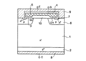
図1は、本発明の第1の実施形態である電力用半導体素子の断面図である。以下、電力用半導体素子の一例としてプレーナ構造を有するIGBTを用いて説明する。以下の全ての実施形態では第1導電型層としてn型、第2導電型層としてp型を用いる。
【0022】
図中、1は高抵抗のn型ベース層を示しており、このn型ベース層1の一方の面には、高不純物濃度のp型コレクタ層2が形成されている。
【0023】
また、ゲート絶縁膜3およびゲート絶縁膜3と同じ材質ではあるが厚さの異なるゲート絶縁膜10を介してゲート電極5が形成されている。n型ベース層1の表面にはp型ベース層6が形成されている。このp型ベース層6の表面には、高不純物濃度のn型エミッタ層7が形成されている。
【0024】
また、上記p型ベース層6は、不純物の注入および熱拡散によって形成されることから、不純物濃度分布はガウス分布に準じる分布になっており、チャネル領域CHにおいても同様である。
【0025】
n型ベース層1、p型ベース層6、n型エミッタ層7、ゲート絶縁膜3、ゲート絶縁膜10およびゲート電極5によって、ゲート絶縁膜3およびゲート絶縁膜10とp型ベース層6の界面にチャネルCHが形成されn型エミッタ層7からn型ベース層1に電子を注入するMOSFETを構成している。
【0026】
p型コレクタ層2上にはコレクタ電極8が設けられている。また、n型エミッタ層7およびp型ベース層6上にはエミッタ電極9が設けられている。n型エミッタ層7とp型ベース層6はこのエミッタ電極9によって短絡している。また、ゲート電極5上には層間絶縁膜4が設けられていて、エミッタ電極9と接しないようになっている。
【0027】
次にこのIGBTの動作を以下に説明する。ターンオン時には、エミッタ電極9とコレクタ電極8との間にコレクタ電圧VCEが印加された状態で、エミッタ電極9とゲート電極5との間に所定の正のゲート電圧VGEを印加すると、チャネル領域CHがn型に反転しチャネルが形成される。このチャネルを通じてエミッタ電極9から電子がn型ベース層1に注入される。この注入された電子によりp型コレクタ層2とn型ベース層1との間が順バイアスされ、正孔がp型コレクタ層2よりn型ベース層1に注入される。この結果、伝導度変調によりn型ベース層1の抵抗が大幅に低減して通電する。
【0028】
一方ターンオフするには、ゲート電極5にエミッタ電極9に対して負の電圧が印加される。これによって、p型ベース層6とゲート絶縁膜3およびゲート絶縁膜10に接した位置に形成されていた反転層が消失して、電子注入が停止する。一方、n型ベース層1内に蓄積されていた正孔hは、その一部がp型ベース層6を介してエミッタ電極9に排出され、残りの正孔hが電子eと再結合して消滅し、素子はターンオフする。
【0029】
ここで素子が負荷短絡状態になった場合、素子は導通状態でコレクタ電極8に電源電圧が印加され、これによって素子には短絡ピーク電流(Icp)が流れ、ある一定時間(tsc)で素子は破壊する。負荷が短絡してから素子破壊に至るまでの時間が負荷短絡耐量(tsc)である。
【0030】
ここで、このIGBTの短絡ピーク電流が大きくなると負荷短絡耐量は小さくなることが確認されている。この理由は短絡ピーク電流による熱破壊である。本発明による新構造のIGBTでは、短絡ピーク電流とほぼ同じ静特性で電流の飽和値を小さくすることによって負荷短絡耐量を大きくすることができる。
【0031】
以下に上記した本発明の構成により負荷短絡耐量が向上する理由を述べる。
【0032】
一般に、オン状態にあるIGBTにさらにコレクタ電圧VCEを増大すると、それに伴ってp型ベース層6のチャネル部分CHの点Q2での電位も上昇し、ゲート電位と点Q2でのベース電位との電位差がしきい値電圧よりも小さくなり反転層を維持することが出来なくなって空乏化(ピンチオフ)し抵抗が無限大となり、IGBTの電流は飽和する。しきい値電圧は、ゲート絶縁膜のキャパシタンスの容量と反比例の関係があり、キャパシタンス容量が増大するにつれ、しきい値電圧は低下する。
【0033】
本実施形態ではチャネル部分CHにおいて、しきい値電圧は、上記のしきい値電圧とゲート絶縁膜のキャパシタンスの関係よりゲート絶縁膜3に接するp型ベース層6領域よりもゲート絶縁膜3の膜厚よりも厚い膜厚を有するゲート絶縁膜10に接するp型ベース層6領域の点Q2で決まり、したがって、ピンチオフもこのゲート絶縁膜10に接するp型ベース層6領域の点Q2で起こる。
【0034】
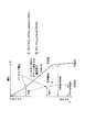
次に従来のIGBTの電流の飽和値よりも本発明のIGBTの電流の飽和値が小さくなることを示す。図7は、縦軸にn型エミッタ層7とエミッタ電極9の境界を原点にとりエミッタ電極9からコレクタ電極8への距離を示し、横軸にエミッタ電極9を基準(接地)とした電圧分布を、図11(従来技術のプレーナIGBT)のX−X′と図1(本発明のプレーナIGBT)のA−A′のぞれぞれに対して示している。
【0035】
この図7より、従来のIGBTは、ピンチオフする電圧Vpin と、ピンチオフ点Q1からn型ベース層101までのチャネル部分の抵抗による電圧Vpin-chと、n型ベース層101とp型コレクタ層102間の電圧Vch-collとを合わせたもの(Vpin +Vpin-ch +Vch-coll =VCE(1) )がコレクタ電圧VCEであり、IGBTの飽和の電流値はこのコレクタ電圧VCEの二乗で変換する。
【0036】
本発明は、ピンチオフ点をゲート絶縁膜10に接するp型ベース層6領域の点Q2にシフトさせることにより、ピンチオフ点Q2からn型ベース層1との間のチャネル部分の抵抗による電圧Vpin-chを取り除くことにより、コレクタ電圧が、ピンチオフ電圧Vpin と、n型ベース層1とp型コレクタ層3間の電圧Vch-coll との足し合わせになるようにしている(Vpin +Vch-coll =VCE(2) )。
【0037】
したがって、本発明のコレクタ電圧VCEは従来のコレクタ電圧VCEよりも小さく、これによって、本発明によるIGBTの飽和の電流値も従来のIGBTでの飽和の電流値にくらべて小さくなる。
【0038】
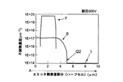
図8は、ゲート酸化膜下の不純物濃度分布を示す図であり、n型エミッタ層7、p型ベース層6、n型ベース層1の不純物濃度を示している。図に示すように、p型ベース層6の不純物濃度は、エミッタ側表面においてエミッタ側にピークを持つガウス分布に準じる分布になっている。
【0039】
図9は、上記のシミュレーションの結果である。具体的には、従来のIGBTでは、p型ベース層107上のゲート絶縁膜103の膜厚が1000オングストロームで、この時の飽和電流値が6800A/cm2であるのに対して、本発明では、p型ベース層6上のゲート酸化膜3を従来のIGBTでのゲート酸化膜103の膜厚と同じ1000オングストロームの膜厚に保ちつつ、ゲート絶縁膜10の膜厚を1μmにした場合、この時の飽和電流値は1700A/cm2となった。研究の結果、この飽和電流値に対応する負荷短絡耐量(tsc)(短絡ピーク電流Icpが流れてから素子の短絡保護回路の動作が開始するまでの所要時間)は10μs以上得られることを確認した。
【0040】
したがって、負荷短絡耐量とIGBTの電流の飽和値との関係から、本発明の電流の飽和値を小さくする方法によって、負荷短絡耐量を大きくすることが出来る。
【0041】
(第2の実施形態)
図2は、本発明の第2の実施形態である電力用半導体素子の断面図である。本実施形態と前述した第1の実施形態を示す図1との違いは、n型ベース層1の表面に接するゲート絶縁膜が、第1の実施形態の図1ではゲート絶縁膜3であったが、本実施形態では、ゲート絶縁膜3よりも膜厚の厚いゲート絶縁膜10であるところである(テラス型ゲート)。図2のプレーナIGBTの動作は、前述した図1のプレーナIGBTの動作と比べて基本的には同じであり、しきい値電圧はゲート絶縁膜10と接するp型ベース層6領域内で決まることから、ピンチオフは、このゲート絶縁膜10と接するp型ベース層6の領域内のQ2で起こる。
【0042】
本実施形態では、n型ベース層1領域内に接するゲート絶縁膜をゲート絶縁膜10にすることによりゲート絶縁膜のキャパシタンス容量が、n型ベース層1領域内にゲート絶縁膜3を有する図1に比べて小さくすることができることにより、ターンオン、ターンオフに要する時間を図1よりも短くすることができる。また、製造工程もより容易である。
【0043】
(第3の実施形態)
図3は、本発明の第3の実施形態である電力用半導体素子の断面図である。本実施形態と前述した第1の実施形態を示す図1との違いは、図1のゲート絶縁膜3が、本実施形態の図3での勾配をもつゲート酸化膜11に対応している点である。このゲート絶縁膜11は、p型ベース層6とn型ベース層1との接合部分上にあるゲート絶縁膜の膜厚を、n型エミッタ層7とp型ベース層6との接合部分上にあるゲート絶縁膜の膜厚よりも厚く、n型エミッタ層7とp型ベース層6との接合部分に近づくにつれゲート絶縁膜の膜厚が徐々に薄くなるよう勾配がついていることが特徴である。
【0044】
図3のプレーナIGBTの動作は、前述した第1の実施形態における図1のプレーナIGBTの動作とくらべて基本的には同じである。本実施形態においては、ゲート絶縁膜11はp型ベース層6とn型ベース層1の接合に近づくにつれ膜厚は厚くなることから、しきい値電圧もp型ベース層6とn型ベース層1の接合に近づくにつれ徐々に高くなる。したがって、前述した図1のプレーナIGBTと同様に点Q2でピンチオフがおこり、前述した第1の実施形態における負荷短絡耐量が向上する理由と同様の理由により、負荷短絡耐量を向上することができる。
【0045】
(第4の実施形態)
図4は、本発明の第4の実施形態である電力用半導体素子の断面図である。図4と第1の実施形態の図1との違いは、図1においては、ゲート絶縁膜3とゲート絶縁膜10との材質が同じであり、したがって、比誘電率も同じであるが、本実施形態の図4においては、ゲート絶縁膜3とゲート絶縁膜12とは材質が異なり、したがって、比誘電率も異なる。本実施形態のゲート絶縁膜の例として、例えば、ゲート絶縁膜3に五酸化タンタル(Ta2 O5 )(比誘電率22)あるいは、窒化シリコン(Si3 N4 )(比誘電率7)を用いて、ゲート絶縁膜12に二酸化シリコン(SiO2 )(比誘電率3.9)を用いることである。これによって、2つのゲート絶縁膜の膜厚がゲート絶縁膜3とゲート絶縁膜12と同じであっても、2つのゲート絶縁膜のキャパシタンス容量は異なることになる。しきい値電圧は、ゲート絶縁膜キャパシタンス容量がゲート絶縁膜3にくらべ小さいゲート絶縁膜12によってきまり、ピンチオフは、ゲート絶縁膜12と接するp型ベース層6のチャネル領域CH点Q2において起こる。
【0046】
したがって、前述した第1の実施形態における負荷短絡耐量が向上する理由と同様の理由により、負荷短絡耐量を向上することができる。
【0047】
(第5の実施形態)
図5は、本発明の第5の実施形態である電力用半導体素子(横型IGBT)の断面図である。図5中、401は高抵抗のn型ベース層であり、このn型ベース層401の一方の面には、p型基板層404が形成されており、このp型基板層404上にはエミッタ電極410が設けられている。また、n型ベース層401の他方の面には、選択的にp型ベース層407が形成されており、このp型ベース層407の表面には選択的に高不純物濃度のn型エミッタ層409が形成される。また、前記n型ベース層401の他方の面には、選択的にn型バッファ層403が形成されており、このn型バッファ層403の表面には選択的に高不純物濃度のp型コレクタ層402が形成され、このp型コレクタ層402に接してコレクタ電極411が形成されている。
【0048】
前記p型ベース層407上の一部、p型ベース層408上、n型ベース層401上の一部およびn型バッファ層上にゲート絶縁膜412が、さらにp型ベース層407上の一部分には、ゲート絶縁膜408が設けられている。このゲート絶縁膜408は、ゲート絶縁膜412と膜厚あるいは比誘電率が異なることによりゲート絶縁膜のキャパシタンス容量が異なっている。ゲート絶縁膜412およびゲート絶縁膜408上にはゲート電極406が設けられている。このゲート電極406上には層間絶縁膜405が設けられており、それに開口されたコンタクトホールを介して前記n型エミッタ層409上の一部およびp型ベース層407上の一部にコンタクトするようにエミッタ電極410が設けられている。なお、前記ゲート電極406は、ゲート絶縁膜412とゲート絶縁膜408と層間絶縁膜405によって、エミッタ電極410、コレクタ電極411、n型ベース層401およびp型ベース層407とは、絶縁されている。
【0049】
図5の横形IGBTの動作は、前述した第1の実施形態における図1のプレーナIGBTの動作とくらべて基本的には同じである。本実施形態においては、ゲート絶縁膜408下のp型ベース層407のチャネル部分CH点Q2でしきい値電圧が決まる。したがって、前述した図1のプレーナIGBTと同様に点Q2でピンチオフがおこり、前述した第1の実施形態における負荷短絡耐量が向上する理由と同様の理由により、負荷短絡耐量を向上することができる。
【0050】
(第6の実施形態)
図6は、本発明の第6の実施形態である電力用半導体素子(トレンチIGBT)の断面図である。
【0051】
図中、301は高抵抗のn型ベース層を示しており、このn型ベース層301の一方の面には、高不純物濃度のp型コレクタ層302が形成されている。
【0052】
また、トレンチ303の内部には、ゲート絶縁膜304およびゲート絶縁膜311を介してゲート電極305が埋め込み形成されている。各トレンチ303で挟まれた領域のn型ベース層301の表面には高不純物濃度のp型ベース層306が形成されている。
【0053】
このp型ベース層306の表面には高不純物濃度のn型エミッタ層307が形成されている。n型ベース層301、p型ベース層306、n型エミッタ層307、ゲート絶縁膜304、ゲート絶縁膜311およびゲート電極305によって、トレンチ303に接したp型ベース層306の表面にチャネルCHが形成されn型エミッタ層307からn型ベース層301に電子を注入するMOSFETを構成している。
【0054】
p型コレクタ層302上にはコレクタ電極308が設けられている。また、n型エミッタ層307およびp型ベース層306上にはエミッタ電極309が設けられている。n型エミッタ層307とp型ベース層306はこのエミッタ電極309によって短絡している。また、ゲート電極305上には層間絶縁膜310が設けられていて、エミッタ電極309と接しないようになっている。
【0055】
次にこのIGBTの動作を以下に説明する。ターンオン時には、エミッタ電極309とコレクタ電極308との間にコレクタ電圧VCEが印加された状態で、エミッタ電極309とゲート電極305との間に所定の正のゲート電圧VGEを印加すると、チャネル領域がn型に反転しチャネルCHが形成される。このチャネルCHを通じてエミッタ電極309から電子がn型ベース層301に注入される。この注入された電子によりp型コレクタ層302とn型ベース層301との間が順バイアスされ、正孔がp型コレクタ層302よりn型ベース層301に注入される。この結果、伝導度変調によりn型ベース層301の抵抗が大幅に低減して通電する。
【0056】
一方ターンオフするには、ゲート電極305にエミッタ電極309に対して負の電圧が印加される。これによって、p型ベース層306のゲート電極305に接した位置に形成されていた反転層が消失して、電子注入が停止する。一方、n型ベース層内に蓄積されていた正孔hは、その一部がp型ベース層306を介してエミッタ電極309に排出され、残りの正孔hが電子eと再結合して消滅し、素子はターンオフする。
【0057】
ここで素子が負荷短絡状態になった場合、素子は導通状態でコレクタ電極308に電源電圧が印加され、これによって素子には短絡ピーク電流(Icp)が流れ、ある一定時間(tsc)で素子は破壊する。負荷が短絡してから素子破壊に至るまでの時間が負荷短絡耐量(tsc)である。
【0058】
ここで、このIGBTの短絡ピーク電流が大きくなると負荷短絡耐量は小さくなることが確認されている。この理由は短絡ピーク電流による熱破壊である。本発明による新構造のIGBTでは、短絡ピーク電流とほぼ同じ静特性での電流の飽和値を小さくすることによって負荷短絡耐量を大きくすることができる。
【0059】
以下、本発明で負荷短絡耐量が向上する理由を述べる。
【0060】
一般に、オン状態にあるIGBTにさらにコレクタ電圧VCEを増大すると、それに伴ってp型ベース層306のチャネル部分CHの点Q2での電位も上昇し、ゲート電位と点Q2でのベース電位との電位差が閾値電圧よりも小さくなり反転層を維持することが出来なくなって空乏化(ピンチオフ)し抵抗が無限大となり、IGBTの電流は飽和する。本実施形態では、チャネル部分CHにおいて閾値電圧は、第1の実施形態と同様の理由により、ゲート絶縁膜311で決まる。したがって、ピンチオフもこのゲート絶縁膜311に接するp型ベース層306の点Q2で起こる。
【0061】
次に従来のIGBTの電流の飽和値よりも本発明のIGBTの電流の飽和値が小さくなることを示す。
【0062】
本発明は、ピンチオフ点をゲート絶縁膜311に接するp型ベース層306にシフトさせることによりピンチオフ点からn型ベース層307との間のチャネル部分の抵抗による電圧Vpin-ch を取り除くことにより、コレクタ電圧が、ピンチオフ電圧Vpin と、n型ベース層301とp型コレクタ層302間の電圧Vch-coll との足し合わせになるようにしている(Vpin +Vch-coll =VCE(2) )。したがって、本発明のコレクタ電圧VCEは従来のコレクタ電圧VCEよりも小さく、これによって、本発明によるIGBTの飽和の電流値も従来のIGBTでの飽和の電流値に較べて小さくなる。よって、負荷短絡耐量は向上する。
【0063】
(第7の実施形態)
図10は、本発明の第7の実施形態である電力用半導体素子(パワーMOSFET)の断面図である。
【0064】
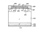
図10のパワーMOSFETは、前述した図1のプレーナIGBTとくらべて、p型不純物で形成されたコレクタ層2の代わりに、n型不純物で形成されたドレイン層202になり、コレクタ電極8がドレイン電極208となり、n型エミッタ層7がn型ソース層207となり、エミッタ電極9がソース電極209となっている点が異なり、その他は同じである。
【0065】
一般に、オン状態にあるパワーMOSFETにさらにドレイン電圧VSDを増大すると、それに伴ってp型ベース層206のチャネル部分CHの点Q2での電位も上昇し、ゲート電位と点Q2でのベース電位との電位差が閾値電圧よりも小さくなり反転層を維持することが出来なくなって空乏化(ピンチオフ)し抵抗が無限大となり、パワーMOSFETの電流は飽和する。本実施形態では、チャネル部分CHにおいて閾値電圧は、第1の実施形態と同様の理由により、ゲート絶縁膜210で決まる。したがって、ピンチオフもこのゲート絶縁膜210に接するp型ベース層206の点Q2で起こる。
【0066】
次に従来のパワーMOSFETの電流の飽和値よりも本発明のパワーMOSFETの電流の飽和値が小さくなることを示す。
【0067】
本発明は、ピンチオフ点をゲート絶縁膜210に接するp型ベース層206にシフトさせることによりピンチオフ点からn型ソース層207との間のチャネル部分の抵抗による電圧Vpin-ch を取り除くことにより、コレクタ電圧を、ピンチオフ電圧Vpin と、n型ベース層201とp型ドレイン層202間の電圧Vch-collとの足し合わせになるようにしている(Vpin +Vch-coll =VCE(2) )。したがって、本発明のドレイン電圧VSDは従来のドレイン電圧VSDよりも小さく、これによって、本発明によるパワーMOSFETの飽和の電流値も従来のパワーMOSFETでの飽和の電流値にくらべて小さくなる。よって、負荷短絡耐量は向上する。
【0068】
【発明の効果】
上述したように本発明によれば、低いオン電圧を維持しつつ、負荷短絡時に生じる短絡ピーク電流を抑えることによって高い負荷短絡耐量を実現し得る電力用半導体素子及びその製造方法を提供することができる。
【図面の簡単な説明】
【図1】本発明の電力用半導体素子の第1の実施形態に係わるプレーナIGBTを示す断面図である。
【図2】本発明の電力用半導体素子の第2の実施形態に係わるプレーナIGBTを示す断面図である。
【図3】本発明の電力用半導体素子の第3の実施形態に係わるプレーナIGBTを示す断面図である。
【図4】本発明の電力用半導体素子の第4の実施形態に係わるプレーナIGBTを示す断面図である。
【図5】本発明の電力用半導体素子の第5の実施形態に係わるプレーナIGBTを示す断面図である。
【図6】本発明の電力用半導体素子の第6の実施形態に係わるプレーナIGBTを示す断面図。
【図7】図11に示す従来のプレーナIGBTのX−X′に沿った電圧分布と、図1に示す本発明のプレーナIGBTのA−A′に沿った電圧分布とを対比して示す図である。
【図8】ゲート絶縁膜下の不純物濃度分布を示す図である。
【図9】図1のトレンチIGBTのコレクタ電圧対コレクタ電流静特性をシミュレーションした結果と、従来のプレーナIGBTのコレクタ電圧対コレクタ電流静特性をシミュレーションした結果とを対比して示す図である。
【図10】本発明の電力用半導体素子の第7の実施形態に係わるプレーナIGBTを示す断面図である。
【図11】従来のプレーナIGBTを示す断面図である。
【符号の説明】
1 n型ベース層
2 p型コレクタ層
3 ゲート絶縁膜
4 層間絶縁膜
5 ゲート電極
6 p型ベース層
7 n型エミッタ層
8 コレクタ電極
9 エミッタ電極
10 ゲート絶縁膜
11 ゲート絶縁膜
12 ゲート絶縁膜[0001]
BACKGROUND OF THE INVENTION
The present invention relates to an IGBT and a power MOSFET among power semiconductor elements constituting a power conversion device such as an inverter, and more particularly to an element structure with improved load short-circuit tolerance.
[0002]
[Prior art]
In response to the recent demand for miniaturization and high performance of power supply equipment in the field of power electronics, power semiconductor devices have high breakdown voltage and high current, as well as low loss, high destruction resistance, and high speed performance. Improvement is focused on. In particular, an IGBT capable of obtaining a lower on-voltage than a power MOSFET is used as a power semiconductor element having a withstand voltage of about 300 V or higher in terms of higher withstand voltage and higher current.
[0003]
As this type of IGBT, two types are widely known: a planar structure in which a gate is provided in a flat plate shape and a trench structure in which a gate is embedded in a premises.
[0004]
FIG. 11 is a cross-sectional view showing the configuration of an IGBT having this type of planar structure. In this IGBT, a high-concentration p-
[0005]
A
[0006]
The n-
[0007]
In the conventional planar IGBT having the above structure, the n-
[0008]
Next, the operation of the IGBT will be described. Since the principle of operation of the planar structure IGBT and the trench structure IGBT is the same, the operation of the planar structure IGBT will be described below.
[0009]
When a positive voltage is applied to the
[0010]
On the other hand, to turn off, a negative voltage is applied to the
[0011]
Here, when the element is in a load short-circuit state, the element is in a conductive state and a power supply voltage is applied to the
[0012]
[Problems to be solved by the invention]
As described above, the conventional semiconductor element has a problem that the load short-circuit resistance is small.
[0013]
The present invention has been made in view of the above circumstances, and a power semiconductor device capable of simultaneously realizing a high load short-circuit withstand capability while maintaining a low on-voltage.And its manufacturing methodIs to provide.
[0014]
[Means for Solving the Problems]
To achieve the above objective,A first aspect of the present invention is a power semiconductor element,A first conductivity type base layer; a second conductivity type base layer selectively formed on one surface of the first conductivity type base layer; and a surface selectively formed on the surface of the second conductivity type base layer. First conductivity type emitterLayer and, Of the first conductivity type base layerOn one of the other surfacesSelectively formed collectorLayer andThe collector layerFormed onA first main electrode and the first conductivity type emitter layer;Above andA second main electrode formed on the second conductivity type base layer;Including a first insulating portion and a second insulating portion;The first conductivity type emitterLayer andThe second conductivity type base layer between the first conductivity type base layersFormed in direct contact with the surface ofA gate insulating film;Formed above the first insulating portion and the second insulating portion;A gate electrode, and the second electrodeInsulationThe capacitance of the first capacitance is the firstInsulationCapacitance capacitySmaller than.
According to a second aspect of the present invention, in the first aspect, the first insulating portion is formed at a position close to the first conductive type emitter layer, and the second insulating portion is the first conductive type. It is formed at a position close to the base layer.
According to a third aspect of the present invention, in the second aspect, the thickness of the second insulating portion is larger than the thickness of the first insulating portion.
[0015]
According to a fourth aspect of the present invention, in the second aspect, the relative dielectric constant of the second insulating portion is smaller than the relative dielectric constant of the first insulating portion.
According to a fifth aspect of the present invention, in the second aspect, the thickness of the second insulating portion has a gradient, and the thickness of the first conductivity type emitter side is equal to the first conductivity type base layer side. Is less than the thickness.
According to a sixth aspect of the present invention, in any one of the first to fifth aspects, the gate electrode penetrates the second conductive type base layer from the surface of the first conductive type emitter layer. The trench is formed so as to reach a middle depth of the first conductivity type base layer through the first insulating portion and the second insulating portion.
[0016]
According to a seventh aspect of the present invention, there is provided a method for manufacturing a power semiconductor device, comprising: forming a first conductivity type base layer; and forming a second conductivity type on one surface of the first conductivity type base layer. Selectively forming a base layer; selectively forming a first conductivity type emitter layer on a surface of the second conductivity type base layer; and forming one or the other surface of the first conductivity type base layer. Forming a collector layer selectively on one side, forming a first main electrode on the collector layer, a second layer on the first conductive type emitter layer and the second conductive type base layer; Forming a main electrode, and a first insulating portion and a second insulating portion, and in direct contact with the surface of the second conductivity type base layer between the first conductivity type emitter layer and the first conductivity type base layer Forming a gate insulating film, and forming the first insulating portion and the second insulating portion. Anda forming a gate electrode toward the capacity of the capacitance of the second insulating portion is smaller than the capacitance of the capacitance of the first insulating portion.
According to an eighth aspect of the present invention, in the seventh aspect, the first insulating portion is formed at a position close to the first conductive type emitter layer, and the second insulating portion is the first conductive type. It is formed at a position close to the base layer.
According to a ninth aspect of the present invention, in the eighth aspect, the thickness of the second insulating portion is greater than the thickness of the first insulating portion.
According to a tenth aspect of the present invention, in the eighth aspect, the relative dielectric constant of the second insulating portion is smaller than the relative dielectric constant of the first insulating portion.
According to an eleventh aspect of the present invention, in the eighth aspect, the thickness of the second insulating portion has a gradient, and the thickness of the first conductivity type emitter side is equal to the first conductivity type base layer side. Less than the thickness of
According to a twelfth aspect of the present invention, in any one of the seventh to eleventh aspects, the gate electrode penetrates the second conductivity type base layer from the surface of the first conductivity type emitter layer. A trench structure embedded in the trench formed so as to reach a middle depth of the first conductivity type base layer through the first insulating portion and the second insulating portion;
According to a thirteenth aspect of the present invention, there is provided a power semiconductor device comprising a first conductivity type base layer and a second conductivity type base selectively formed on one surface of the first conductivity type base layer. A first conductive type source layer selectively formed on the surface of the second conductive type base layer, and selectively formed on one of the one and other surfaces of the first conductive type base layer. A drain layer; a first main electrode formed on the drain layer; a second main electrode formed on the first conductivity type source layer; and the second conductivity type base layer; a first insulation; A gate insulating film formed in direct contact with the surface of the second conductivity type base layer between the first conductivity type source layer and the first conductivity type base layer, A first insulating portion and a gate electrode formed above the second insulating portion, and the second insulating portion. Capacity of capacitance is smaller than the capacitance of the capacitance of the first insulating portion.
According to a fourteenth aspect of the present invention, in the thirteenth aspect, the first insulating portion is formed at a position close to the first conductive type source layer, and the second insulating portion is the first conductive type. It is formed at a position close to the base layer.
[0017]
According to a fifteenth aspect of the present invention, in the fourteenth aspect, the thickness of the second insulating portion is larger than the thickness of the first insulating portion.
According to a sixteenth aspect of the present invention, in the fourteenth aspect, the relative dielectric constant of the second insulating portion is smaller than the relative dielectric constant of the first insulating portion.
According to a seventeenth aspect of the present invention, in the fourteenth aspect, the thickness of the second insulating portion has a gradient, and the thickness of the first conductivity type source side is equal to the first conductivity type base layer side. Less than the thickness of
According to an eighteenth aspect of the present invention, in any one of the thirteenth to seventeenth aspects, the gate electrode penetrates the second conductivity type base layer from the surface of the first conductivity type source layer. A trench structure embedded in the trench formed so as to reach a middle depth of the first conductivity type base layer through the first insulating portion and the second insulating portion;
[0018]
According to a nineteenth aspect of the present invention, there is provided a method for manufacturing a power semiconductor device, comprising: forming a first conductivity type base layer; and forming a second conductivity type on one surface of the first conductivity type base layer. Selectively forming a base layer; selectively forming a first conductivity type source layer on a surface of the second conductivity type base layer; and forming one or the other surface of the first conductivity type base layer. Forming a drain layer selectively on one, forming a first main electrode on the drain layer, a second on the first conductivity type source layer and on the second conductivity type base layer; Forming a main electrode, and a first insulating part and a second insulating part, and directly contacting the surface of the second conductive type base layer between the first conductive type source layer and the first conductive type base layer Forming a gate insulating film, and above the first insulating portion and the second insulating portion. Comprising forming a gate electrode, the capacitance of the capacitance of the second insulating portion is smaller than the capacitance of the capacitance of the first insulating portion.
[0019]
According to a twentieth aspect of the present invention, in the nineteenth aspect, the first insulating portion is formed at a position close to the first conductive type source layer, and the second insulating portion is the first conductive type. 20. The method for manufacturing a power semiconductor element according to
According to a twenty-first aspect of the present invention, in the twentieth aspect, the thickness of the second insulating portion is larger than the thickness of the first insulating portion.
According to a twenty-second aspect of the present invention, in the twentieth aspect, the relative dielectric constant of the second insulating portion is smaller than the relative dielectric constant of the first insulating portion.
According to a twenty-third aspect of the present invention, in the twentieth aspect, the thickness of the second insulating portion has a gradient, and the thickness of the first conductivity type source side is equal to the first conductivity type base layer side. Is less than the thickness.
According to a twenty-fourth aspect of the present invention, in any one of the nineteenth to twenty-third aspects, the gate electrode penetrates the second conductive type base layer from the surface of the first conductive type source layer. A trench structure embedded in the trench formed so as to reach a halfway depth of the first conductivity type base layer via the first insulating portion and the second insulating portion;
[0020]
DETAILED DESCRIPTION OF THE INVENTION
Hereinafter, embodiments of the present invention (hereinafter referred to as embodiments) will be described with reference to the drawings.
[0021]
(First embodiment)
FIG. 1 is a cross-sectional view of a power semiconductor device according to a first embodiment of the present invention. Hereinafter, description will be made using an IGBT having a planar structure as an example of a power semiconductor element. In all the following embodiments, the n-type is used as the first conductivity type layer and the p-type is used as the second conductivity type layer.
[0022]
In the figure,
[0023]
Further, the
[0024]
In addition, since the p-
[0025]
The n-
[0026]
A
[0027]
Next, the operation of this IGBT will be described below. At the time of turn-on, when a predetermined positive gate voltage VGE is applied between the
[0028]
On the other hand, to turn off, a negative voltage is applied to the
[0029]
Here, when the element is in a load short-circuit state, the element is in a conductive state and a power supply voltage is applied to the
[0030]
Here, it is confirmed that the load short-circuit withstand capability decreases as the short-circuit peak current of the IGBT increases. The reason for this is thermal breakdown due to short-circuit peak current. In the IGBT having a new structure according to the present invention, the load short-circuit withstand capability can be increased by reducing the saturation value of the current with substantially the same static characteristics as the short-circuit peak current.
[0031]
The reason why the load short-circuit resistance is improved by the configuration of the present invention described above will be described below.
[0032]
In general, when the collector voltage VCE is further increased to the IGBT in the on state, the potential at the point Q2 of the channel portion CH of the p-
[0033]
In this embodiment, in the channel portion CH, the threshold voltage is a film of the
[0034]
Next, it is shown that the saturation value of the current of the IGBT of the present invention is smaller than the saturation value of the current of the conventional IGBT. In FIG. 7, the vertical axis indicates the distance from the
[0035]
From FIG. 7, the conventional IGBT has a pinch-off voltage VpinAnd the voltage V due to the resistance of the channel portion from the pinch-off point Q1 to the n-
[0036]
The present invention shifts the pinch-off point to the point Q2 of the p-
[0037]
Therefore, the collector voltage VCE of the present invention is smaller than the conventional collector voltage VCE, and accordingly, the saturation current value of the IGBT according to the present invention is smaller than the saturation current value of the conventional IGBT.
[0038]
FIG. 8 is a diagram showing the impurity concentration distribution under the gate oxide film, and shows the impurity concentrations of the n-
[0039]
FIG. 9 shows the result of the above simulation. Specifically, in the conventional IGBT, the thickness of the
[0040]
Therefore, from the relationship between the load short-circuit tolerance and the saturation value of the IGBT current, the load short-circuit tolerance can be increased by the method of reducing the current saturation value of the present invention.
[0041]
(Second Embodiment)
FIG. 2 is a sectional view of a power semiconductor device according to the second embodiment of the present invention. The difference between this embodiment and FIG. 1 showing the first embodiment is that the gate insulating film in contact with the surface of the n-
[0042]
In this embodiment, the gate insulating film in contact with the n-
[0043]
(Third embodiment)
FIG. 3 is a sectional view of a power semiconductor device according to the third embodiment of the present invention. The difference between this embodiment and FIG. 1 showing the first embodiment described above is that the
[0044]
The operation of the planar IGBT of FIG. 3 is basically the same as the operation of the planar IGBT of FIG. 1 in the first embodiment described above. In this embodiment, since the
[0045]
(Fourth embodiment)
FIG. 4 is a sectional view of a power semiconductor device according to the fourth embodiment of the present invention. The difference between FIG. 4 and FIG. 1 of the first embodiment is that, in FIG. 1, the materials of the
[0046]
Therefore, the load short-circuit tolerance can be improved for the same reason as that for improving the load short-circuit tolerance in the first embodiment described above.
[0047]
(Fifth embodiment)
FIG. 5 is a cross-sectional view of a power semiconductor device (horizontal IGBT) according to a fifth embodiment of the present invention. In FIG. 5,
[0048]
A
[0049]
The operation of the lateral IGBT of FIG. 5 is basically the same as the operation of the planar IGBT of FIG. 1 in the first embodiment described above. In this embodiment, the threshold voltage is determined by the channel portion CH point Q2 of the p-
[0050]
(Sixth embodiment)
FIG. 6 is a sectional view of a power semiconductor element (trench IGBT) according to a sixth embodiment of the present invention.
[0051]
In the figure,
[0052]
A
[0053]
An n-
[0054]
A
[0055]
Next, the operation of this IGBT will be described below. At the turn-on time, when a predetermined positive gate voltage VGE is applied between the
[0056]
On the other hand, to turn off, a negative voltage is applied to the
[0057]
Here, when the element is in a load short-circuit state, the element is in a conductive state, and a power supply voltage is applied to the
[0058]
Here, it is confirmed that the load short-circuit withstand capability decreases as the short-circuit peak current of the IGBT increases. The reason for this is thermal breakdown due to short-circuit peak current. In the IGBT of the new structure according to the present invention, the load short-circuit withstand capability can be increased by reducing the saturation value of the current with substantially the same static characteristics as the short-circuit peak current.
[0059]
Hereinafter, the reason why the load short-circuit resistance is improved in the present invention will be described.
[0060]
In general, when the collector voltage VCE is further increased to the IGBT in the on state, the potential at the point Q2 of the channel portion CH of the p-
[0061]
Next, it is shown that the saturation value of the current of the IGBT of the present invention is smaller than the saturation value of the current of the conventional IGBT.
[0062]
The present invention shifts the pinch-off point to the p-
[0063]
(Seventh embodiment)
FIG. 10 is a sectional view of a power semiconductor device (power MOSFET) according to the seventh embodiment of the present invention.
[0064]
Compared with the planar IGBT of FIG. 1 described above, the power MOSFET of FIG. 10 becomes the
[0065]
In general, when the drain voltage VSD is further increased in the power MOSFET in the on state, the potential at the point Q2 of the channel portion CH of the p-
[0066]
Next, it will be shown that the saturation value of the current of the power MOSFET of the present invention is smaller than the saturation value of the current of the conventional power MOSFET.
[0067]
The present invention shifts the pinch-off point to the p-
[0068]
【The invention's effect】
As described above, according to the present invention, a power semiconductor device capable of realizing a high load short-circuit withstand capability by suppressing a short-circuit peak current generated when a load is short-circuited while maintaining a low on-voltage.And its manufacturing methodCan be provided.
[Brief description of the drawings]
FIG. 1 is a cross-sectional view showing a planar IGBT according to a first embodiment of a power semiconductor device of the present invention.
FIG. 2 is a cross-sectional view showing a planar IGBT according to a second embodiment of the power semiconductor device of the present invention.
FIG. 3 is a cross-sectional view showing a planar IGBT according to a third embodiment of the power semiconductor device of the present invention.
FIG. 4 is a cross-sectional view showing a planar IGBT according to a fourth embodiment of the power semiconductor element of the present invention.
FIG. 5 is a cross-sectional view showing a planar IGBT according to a fifth embodiment of the power semiconductor element of the present invention.
FIG. 6 is a cross-sectional view showing a planar IGBT according to a sixth embodiment of the power semiconductor element of the present invention.
7 is a diagram showing the voltage distribution along the line XX ′ of the conventional planar IGBT shown in FIG. 11 and the voltage distribution along the line AA ′ of the planar IGBT of the present invention shown in FIG. It is.
FIG. 8 is a diagram showing an impurity concentration distribution under a gate insulating film.
FIG. 9 is a diagram showing a result of simulating the collector voltage vs. collector current static characteristics of the trench IGBT of FIG. 1 and a result of simulating the collector voltage vs. collector current static characteristics of a conventional planar IGBT.
FIG. 10 is a cross-sectional view showing a planar IGBT according to a seventh embodiment of the power semiconductor element of the present invention.
FIG. 11 is a cross-sectional view showing a conventional planar IGBT.
[Explanation of symbols]
1 n-type base layer
2 p-type collector layer
3 Gate insulation film
4 Interlayer insulation film
5 Gate electrode
6 p-type base layer
7 n-type emitter layer
8 Collector electrode
9 Emitter electrode
10 Gate insulation film
11 Gate insulation film
12 Gate insulation film
Claims (24)
第1導電型ベース層と、
前記第1導電型ベース層の一方の表面に選択的に形成された第2導電型ベース層と、
前記第2導電型ベース層の表面に選択的に形成された第1導電型エミッタ層と、
前記第1導電型ベース層の一方及び他方の表面の1つに選択的に形成されたコレクタ層と、
前記コレクタ層上に形成された第1の主電極と、
前記第1導電型エミッタ層上及び前記第2導電型ベース層上に形成された第2の主電極と、
第1絶縁部と第2絶縁部とを含み、前記第1導電型エミッタ層と前記第1導電型ベース層間の前記第2導電型ベース層の表面に直接接触させて形成されたゲート絶縁膜と、
前記第1絶縁部と前記第2絶縁部の上方に形成されたゲート電極と、を具備し、
前記第2絶縁部のキャパシタンスの容量は、前記第1絶縁部のキャパシタンスの容量よりも小さいことを特徴とする電力用半導体素子。 A power semiconductor element,
A first conductivity type base layer;
A second conductivity type base layer selectively formed on one surface of the first conductivity type base layer;
A first conductivity type emitter layer selectively formed on a surface of the second conductivity type base layer;
A collector layer selectively formed on one of one and other surfaces of the first conductivity type base layer;
A first main electrode formed on the collector layer ;
A second main electrode formed on the first conductivity type emitter layer and the second conductivity type base layer;
A gate insulating film including a first insulating part and a second insulating part, and formed in direct contact with the surface of the second conductive type base layer between the first conductive type emitter layer and the first conductive type base layer; ,
A gate electrode formed above the first insulating part and the second insulating part ;
The power semiconductor element, wherein a capacitance of the second insulating part is smaller than a capacitance of the first insulating part .
第1導電型ベース層を形成することと、 Forming a first conductivity type base layer;
前記第1導電型ベース層の一方の表面に第2導電型ベース層を選択的に形成することと、 Selectively forming a second conductivity type base layer on one surface of the first conductivity type base layer;
前記第2導電型ベース層の表面に第1導電型エミッタ層を選択的に形成することと、 Selectively forming a first conductivity type emitter layer on a surface of the second conductivity type base layer;
前記第1導電型ベース層の一方及び他方の表面の1つにコレクタ層を選択的に形成することと、 Selectively forming a collector layer on one of one and other surfaces of the first conductivity type base layer;
前記コレクタ層上に第1の主電極を形成することと、 Forming a first main electrode on the collector layer;
前記第1導電型エミッタ層上及び前記第2導電型ベース層上に第2の主電極を形成することと、 Forming a second main electrode on the first conductivity type emitter layer and the second conductivity type base layer;
第1絶縁部と第2絶縁部とを含み、前記第1導電型エミッタ層と前記第1導電型ベース層間の前記第2導電型ベース層の表面に直接接触させてゲート絶縁膜を形成することと、 Forming a gate insulating film including a first insulating portion and a second insulating portion, in direct contact with the surface of the second conductive type base layer between the first conductive type emitter layer and the first conductive type base layer; When,
前記第1絶縁部と前記第2絶縁部の上方にゲート電極を形成することと、を具備し、 Forming a gate electrode above the first insulating part and the second insulating part, and
前記第2絶縁部のキャパシタンスの容量は、前記第1絶縁部のキャパシタンスの容量よりも小さいことを特徴とする電力用半導体素子の製造方法。 The method of manufacturing a power semiconductor device, wherein a capacitance of the second insulating part is smaller than a capacitance of the first insulating part.
第1導電型ベース層と、 A first conductivity type base layer;
前記第1導電型ベース層の一方の表面に選択的に形成された第2導電型ベース層と、 A second conductivity type base layer selectively formed on one surface of the first conductivity type base layer;
前記第2導電型ベース層の表面に選択的に形成された第1導電型ソース層と、 A first conductivity type source layer selectively formed on a surface of the second conductivity type base layer;
前記第1導電型ベース層の一方及び他方の表面の1つに選択的に形成されたドレイン層と、 A drain layer selectively formed on one of one and other surfaces of the first conductivity type base layer;
前記ドレイン層上に形成された第1の主電極と、 A first main electrode formed on the drain layer;
前記第1導電型ソース層上及び前記第2導電型ベース層上に形成された第2の主電極と、 A second main electrode formed on the first conductivity type source layer and the second conductivity type base layer;
第1絶縁部と第2絶縁部とを含み、前記第1導電型ソース層と前記第1導電型ベース層間の前記第2導電型ベース層の表面に直接接触させて形成されたゲート絶縁膜と、 A gate insulating film including a first insulating part and a second insulating part, and formed in direct contact with the surface of the second conductive type base layer between the first conductive type source layer and the first conductive type base layer; ,
前記第1絶縁部と前記第2絶縁部の上方に形成されたゲート電極と、を具備し、 A gate electrode formed above the first insulating part and the second insulating part;
前記第2絶縁部のキャパシタンスの容量は、前記第1絶縁部のキャパシタンスの容量よりも小さいことを特徴とする電力用半導体素子。 The power semiconductor element, wherein a capacitance of the second insulating part is smaller than a capacitance of the first insulating part.
第1導電型ベース層を形成することと、 Forming a first conductivity type base layer;
前記第1導電型ベース層の一方の表面に第2導電型ベース層を選択的に形成することと、 Selectively forming a second conductivity type base layer on one surface of the first conductivity type base layer;
前記第2導電型ベース層の表面に第1導電型ソース層を選択的に形成することと、 Selectively forming a first conductivity type source layer on a surface of the second conductivity type base layer;
前記第1導電型ベース層の一方及び他方の表面の1つにドレイン層を選択的に形成することと、 Selectively forming a drain layer on one of the one and other surfaces of the first conductivity type base layer;
前記ドレイン層上に第1の主電極を形成することと、 Forming a first main electrode on the drain layer;
前記第1導電型ソース層上及び前記第2導電型ベース層上に第2の主電極を形成することと、 Forming a second main electrode on the first conductivity type source layer and the second conductivity type base layer;
第1絶縁部と第2絶縁部とを含み、前記第1導電型ソース層と前記第1導電型ベース層間の前記第2導電型ベース層の表面に直接接触させてゲート絶縁膜を形成することと、 Forming a gate insulating film including a first insulating portion and a second insulating portion, in direct contact with the surface of the second conductive type base layer between the first conductive type source layer and the first conductive type base layer; When,
前記第1絶縁部と前記第2絶縁部の上方にゲート電極を形成することと、を具備し、 Forming a gate electrode above the first insulating part and the second insulating part, and
前記第2絶縁部のキャパシタンスの容量は、前記第1絶縁部のキャパシタンスの容量よりも小さいことを特徴とする電力用半導体素子の製造方法。 The method of manufacturing a power semiconductor device, wherein a capacitance of the second insulating part is smaller than a capacitance of the first insulating part.
Priority Applications (2)
| Application Number | Priority Date | Filing Date | Title |
|---|---|---|---|
| JP2000294316A JP4460741B2 (en) | 2000-09-27 | 2000-09-27 | Power semiconductor device and manufacturing method thereof |
| US09/961,248 US6867454B2 (en) | 2000-09-27 | 2001-09-25 | Power semiconductor device and manufacturing method thereof |
Applications Claiming Priority (1)
| Application Number | Priority Date | Filing Date | Title |
|---|---|---|---|
| JP2000294316A JP4460741B2 (en) | 2000-09-27 | 2000-09-27 | Power semiconductor device and manufacturing method thereof |
Publications (3)
| Publication Number | Publication Date |
|---|---|
| JP2002110980A JP2002110980A (en) | 2002-04-12 |
| JP2002110980A5 JP2002110980A5 (en) | 2006-03-09 |
| JP4460741B2 true JP4460741B2 (en) | 2010-05-12 |
Family
ID=18776947
Family Applications (1)
| Application Number | Title | Priority Date | Filing Date |
|---|---|---|---|
| JP2000294316A Expired - Fee Related JP4460741B2 (en) | 2000-09-27 | 2000-09-27 | Power semiconductor device and manufacturing method thereof |
Country Status (2)
| Country | Link |
|---|---|
| US (1) | US6867454B2 (en) |
| JP (1) | JP4460741B2 (en) |
Families Citing this family (17)
| Publication number | Priority date | Publication date | Assignee | Title |
|---|---|---|---|---|
| US7235862B2 (en) * | 2001-07-10 | 2007-06-26 | National Semiconductor Corporation | Gate-enhanced junction varactor |
| US7081663B2 (en) | 2002-01-18 | 2006-07-25 | National Semiconductor Corporation | Gate-enhanced junction varactor with gradual capacitance variation |
| US7161203B2 (en) * | 2004-06-04 | 2007-01-09 | Micron Technology, Inc. | Gated field effect device comprising gate dielectric having different K regions |
| US20070128810A1 (en) * | 2005-12-07 | 2007-06-07 | Ching-Hung Kao | Ultra high voltage MOS transistor device and method of making the same |
| EP1852916A1 (en) * | 2006-05-05 | 2007-11-07 | Austriamicrosystems AG | High voltage transistor |
| JP5200373B2 (en) * | 2006-12-15 | 2013-06-05 | トヨタ自動車株式会社 | Semiconductor device |
| DE102008045410B4 (en) | 2007-09-05 | 2019-07-11 | Denso Corporation | Semiconductor device with IGBT with built-in diode and semiconductor device with DMOS with built-in diode |
| KR101191281B1 (en) | 2008-03-31 | 2012-10-16 | 미쓰비시덴키 가부시키가이샤 | Semiconductor device |
| JP2011159763A (en) * | 2010-01-29 | 2011-08-18 | Toshiba Corp | Power semiconductor device |
| US8952458B2 (en) | 2011-04-14 | 2015-02-10 | Taiwan Semiconductor Manufacturing Company, Ltd. | Gate dielectric layer having interfacial layer and high-K dielectric over the interfacial layer |
| US10256325B2 (en) * | 2012-11-08 | 2019-04-09 | Infineon Technologies Austria Ag | Radiation-hardened power semiconductor devices and methods of forming them |
| CN103441143B (en) * | 2013-07-10 | 2015-09-09 | 电子科技大学 | There is the anti-breech lock IGBT becoming component mixed crystal emitter region |
| JP2016029707A (en) * | 2014-07-24 | 2016-03-03 | 住友電気工業株式会社 | Silicon carbide semiconductor device |
| JP2016054181A (en) * | 2014-09-03 | 2016-04-14 | トヨタ自動車株式会社 | Insulated gate switching element |
| CN107425060A (en) * | 2016-05-23 | 2017-12-01 | 株洲中车时代电气股份有限公司 | New IGBT structure and preparation method thereof |
| JP7107093B2 (en) * | 2018-08-22 | 2022-07-27 | 株式会社デンソー | switching element |
| CN111129131B (en) * | 2018-10-30 | 2023-09-05 | 株洲中车时代半导体有限公司 | Planar gate IGBT device |
Family Cites Families (8)
| Publication number | Priority date | Publication date | Assignee | Title |
|---|---|---|---|---|
| JPS62126668A (en) * | 1985-11-27 | 1987-06-08 | Mitsubishi Electric Corp | Semiconductor device |
| JP2862027B2 (en) * | 1991-03-12 | 1999-02-24 | 株式会社デンソー | Insulated gate bipolar transistor |
| JPH0685433B2 (en) * | 1992-04-22 | 1994-10-26 | 尚茂 玉蟲 | Vertical structure MOS control thyristor |
| JPH07235672A (en) * | 1994-02-21 | 1995-09-05 | Mitsubishi Electric Corp | Insulated-gate type semiconductor device and manufacture thereof |
| US6117736A (en) * | 1997-01-30 | 2000-09-12 | Lsi Logic Corporation | Method of fabricating insulated-gate field-effect transistors having different gate capacitances |
| JP4192281B2 (en) * | 1997-11-28 | 2008-12-10 | 株式会社デンソー | Silicon carbide semiconductor device |
| KR100268933B1 (en) * | 1997-12-27 | 2000-10-16 | 김영환 | Semiconductor device and method for fabricating the same |
| JP3707942B2 (en) * | 1998-12-17 | 2005-10-19 | 三菱電機株式会社 | Semiconductor device and semiconductor circuit using the same |
-
2000
- 2000-09-27 JP JP2000294316A patent/JP4460741B2/en not_active Expired - Fee Related
-
2001
- 2001-09-25 US US09/961,248 patent/US6867454B2/en not_active Expired - Lifetime
Also Published As
| Publication number | Publication date |
|---|---|
| US20020036311A1 (en) | 2002-03-28 |
| JP2002110980A (en) | 2002-04-12 |
| US6867454B2 (en) | 2005-03-15 |
Similar Documents
| Publication | Publication Date | Title |
|---|---|---|
| JP4460741B2 (en) | Power semiconductor device and manufacturing method thereof | |
| JP4581179B2 (en) | Insulated gate semiconductor device | |
| KR101933244B1 (en) | Insulated gate bipolar transistor | |
| JP5452195B2 (en) | Semiconductor device and power conversion device using the same | |
| US6133607A (en) | Semiconductor device | |
| TWI575736B (en) | Dual trench-gate igbt structure | |
| JP7272775B2 (en) | insulated gate bipolar transistor | |
| JP2002353456A (en) | Semiconductor device and manufacturing method therefor | |
| JPH0758332A (en) | Semiconductor device | |
| WO2013004829A1 (en) | Insulated gate bipolar transistor | |
| US9054152B2 (en) | Semiconductor device | |
| JP4940535B2 (en) | Semiconductor device | |
| JP2006245477A (en) | Semiconductor device | |
| JPH09331063A (en) | High breakdown strength semiconductor device and its manufacturing method | |
| US10297683B2 (en) | Method of manufacturing a semiconductor device having two types of gate electrodes | |
| US20060237786A1 (en) | Power semiconductor device | |
| CN105489644B (en) | IGBT device and preparation method thereof | |
| WO1998026458A1 (en) | Insulated gate semiconductor device | |
| US11264475B2 (en) | Semiconductor device having a gate electrode formed in a trench structure | |
| JPH098322A (en) | Hybrid schottky injection field-effect transistor | |
| CN108305893B (en) | Semiconductor device with a plurality of semiconductor chips | |
| JPH0241182B2 (en) | ||
| JP2004103980A (en) | Semiconductor device | |
| JP2000311998A (en) | Insulated gate turn-off thyristor | |
| CN113644133A (en) | Semiconductor device and preparation method thereof |
Legal Events
| Date | Code | Title | Description |
|---|---|---|---|
| A521 | Written amendment |
Free format text: JAPANESE INTERMEDIATE CODE: A523 Effective date: 20060125 |
|
| A621 | Written request for application examination |
Free format text: JAPANESE INTERMEDIATE CODE: A621 Effective date: 20060125 |
|
| A977 | Report on retrieval |
Free format text: JAPANESE INTERMEDIATE CODE: A971007 Effective date: 20081114 |
|
| TRDD | Decision of grant or rejection written | ||
| A01 | Written decision to grant a patent or to grant a registration (utility model) |
Free format text: JAPANESE INTERMEDIATE CODE: A01 Effective date: 20100119 |
|
| A01 | Written decision to grant a patent or to grant a registration (utility model) |
Free format text: JAPANESE INTERMEDIATE CODE: A01 |
|
| A61 | First payment of annual fees (during grant procedure) |
Free format text: JAPANESE INTERMEDIATE CODE: A61 Effective date: 20100215 |
|
| R151 | Written notification of patent or utility model registration |
Ref document number: 4460741 Country of ref document: JP Free format text: JAPANESE INTERMEDIATE CODE: R151 |
|
| FPAY | Renewal fee payment (event date is renewal date of database) |
Free format text: PAYMENT UNTIL: 20130219 Year of fee payment: 3 |
|
| FPAY | Renewal fee payment (event date is renewal date of database) |
Free format text: PAYMENT UNTIL: 20140219 Year of fee payment: 4 |
|
| LAPS | Cancellation because of no payment of annual fees |