JP4457566B2 - Sputtering method - Google Patents
Sputtering method Download PDFInfo
- Publication number
- JP4457566B2 JP4457566B2 JP2003080273A JP2003080273A JP4457566B2 JP 4457566 B2 JP4457566 B2 JP 4457566B2 JP 2003080273 A JP2003080273 A JP 2003080273A JP 2003080273 A JP2003080273 A JP 2003080273A JP 4457566 B2 JP4457566 B2 JP 4457566B2
- Authority
- JP
- Japan
- Prior art keywords
- emission intensity
- oxygen
- film formation
- argon
- wavelength
- Prior art date
- Legal status (The legal status is an assumption and is not a legal conclusion. Google has not performed a legal analysis and makes no representation as to the accuracy of the status listed.)
- Expired - Fee Related
Links
Images


Landscapes
- Optical Filters (AREA)
- Physical Vapour Deposition (AREA)
Description
【0001】
【発明の属する技術分野】
本発明は主にガラス基板の表面に所定の多層膜光学薄膜、酸化物薄膜等の薄膜を再現性良く形成するスパッタリング方法およびスパッタリング装置に関するものである。
【0002】
【従来の技術】
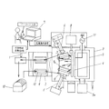
従来のスパッタリング方法およびスパッタリング装置としては、図7に示すものがある。
【0003】
図7は従来のスパッタリング法による多層光学薄膜の形成装置を示すブロック図である。
【0004】
1は薄膜の光学特性を測定する装置、2はロードロック室、3は成膜室、4はスパッタターゲット、5はスパッタターゲット4が複数取り付けられた回転部材、5aは回転部材5を回転させてスパッタターゲット4を切り換えるターゲット切り換えモータ、9は基板、9aは基板9の上に形成された薄膜、6はスパッタ位置において基板9を保持しその位置を制御する基板位置制御手段、7は演算処理、データ管理、装置の駆動制御等を行うコンピュータ、8は水晶式の薄膜モニター、12は基板9と同一外形形状を有する基板ホルダー、10は基板ホルダー12にセットされた基板9を収納するカセット、11はスパッタターゲット4に高周波電圧を印加する高周波電源である。
【0005】
また、基材の表面に多層光学薄膜を形成する方法において、各層の膜厚設定値に基づいて多層光学薄膜を形成し、この形成された多層光学薄膜の光学特性を測定し、この測定された光学特性に基づいて多層光学薄膜が目標の光学特性となるような各層の膜厚を求め、この求められた各層の膜厚に基づいて膜厚設定値を補正し、この補正された膜厚設定値に基づいて次の多層膜光学薄膜を形成する。あるいはスパッタ法により薄膜を形成する方法において、真空室内のH2Oガス濃度または放電インピーダンスを測定し、この測定結果に応じてスパッタ電力、スパッタガス分圧、およびスパッタガス流量のうちの少なくとも1つ以上をスパッタレートが一定に保持されるように制御する。
【0006】
なお、この出願の発明に関する先行技術文献情報としては、例えば特許文献1が知られている。
【0007】
【特許文献1】
特開平7−72307号公報
【0008】
【発明が解決しようとする課題】
しかしながら、前記従来の構成では、装置内のプラズマ状態でないH2O分子を利用するという間接的方法を採用しているため、成膜レートが変化している可能性がある。それはその事象に関する十分な説明がなされていない。
【0009】
つまり、H2O分子についての定量的情報は記載されているが、Hラジカル、H+イオン、H-イオンあるいは酸素原子についての定量的情報、検証データ等において全く記載されていない。また間接的方法を用いるため高い精度を実現する上で問題があると考えられる。
【0010】
本発明は高精度の膜厚測定を実現し、かつ高精度の膜厚制御が実現できるスパッタリング方法およびスパッタリング装置を提供することを目的とするものである。
【0011】
【課題を解決するための手段】
本発明の請求項1に記載の発明は、少なくともアルゴンガスと酸素を用いて基板上に薄膜を形成するスパッタリング方法において、プラズマ発光分光法を用いて前記アルゴンガスでは波長697nmの発光強度と、前記酸素では波長777nmの発光強度とが略等しく、かつその比が一定となるように前記アルゴンガスの流量または酸素流量を調整することで、前記薄膜の成膜レートを一定に制御することを特徴とするスパッタリング方法であり、波長697nmのアルゴン発光強度と波長777nmの酸素発光強度とを用いて両者の波長および発光強度を近い値とすることにより、波長スパンおよびレベル分解能を高めることができるので高精度に評価することができ、その結果、成膜レートを一定に制御して高精度の膜厚制御を実現できる。
【0019】
【発明の実施の形態】
以下、本発明の実施の形態について、図面を参照しながら説明する。
【0020】
(実施の形態1)
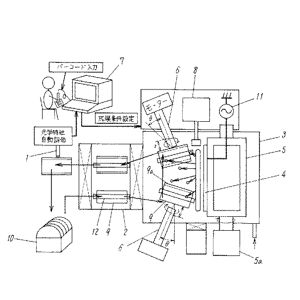
図1は本発明の実施の形態1におけるスパッタリング装置の概略を示す構成図である。
【0021】
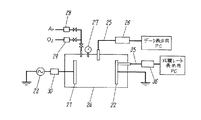
図1において、21はスパッタターゲット、22は基板、23は高周波電源、24は真空チャンバー、25はプラズマモニター用の光ファイバー、26は分光器、27は圧力計、28はアルゴンガス流量計、29は酸素ガス流量計、30は高周波マッチング回路、31〜34は帰還制御ラインである。
【0022】
本発明のスパッタリング装置は、真空チャンバー24の内部に成膜する材料で構成されるスパッタターゲット21を下部電極としての陰極(図示せず)に高周波電源23から高周波マッチング回路30を介して電力が供給される。そして基板22が設置される基板ホルダー(図示せず)を基板側電極22aに有し、スパッタターゲット21と対向するように配置されている。
【0023】
そして、真空チャンバー24の内部には圧力を検知するための圧力計27が配置されている。そして真空チャンバー24の内部を大気から5×10⁻¹Pa程度まで排気するため真空排気ポンプ(図示せず)が備えられ、さらにアルゴンガスや酸素などのスパッタガスを真空チャンバー24の内部に供給できるように配管されている。そして真空チャンバー24の内部にプラズマモニターを備え付け、分光器26で波長697nmのアルゴン発光強度と波長777nmの酸素発光強度を常時モニタリングする。また成膜中の波長697nmのアルゴン発光強度と波長777nmの酸素発光強度の比を一定にするように、成膜中にアルゴンガス流量もしくは酸素ガス流量、真空チャンバー24の内部圧力、シース電位またはプラズマ電位のうち少なくとも一つを変化させることができる構成となっている。
【0024】
以下、薄膜形成方法について説明する。
【0025】
基板22を設置した支持体(図示せず)を基板ホルダー(図示せず)に取り付け、真空ポンプにより真空チャンバー24の内部を約5×10⁻¹Pa程度にまで真空排気する。そして基板22を温度600℃程度にまで加熱し、スパッタガスとしてのアルゴンガス、酸素を導入してスパッタターゲット21に高周波電源23から電力を印加し、スパッタターゲット21からスパッタ粒子が対向する基板22の上に付着して薄膜が形成される。
【0026】
例えば、Ta2O5の成膜条件を(表1)に示す。
【0027】
【表1】
また、図1に示すスパッタターゲット21は厚さ6mm、純度99.9%のTa2O5からなるスパッタターゲット21を用いる。
【0029】
(表1)より高周波電力が1000W、アルゴンガス流量が10sccm、酸素ガス流量が0.4sccm、真空チャンバー24の内部圧力が5.0×10⁻¹Paの条件で成膜を実施することにより、屈折率2.15程度のTa2O5膜が得られる。
【0030】
なお、このときの屈折率の測定波長は632.8nmである。
【0031】
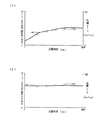
図2(a),(b)は本発明の実施の形態1におけるアルゴン発光強度と酸素発光強度との比と成膜レートの推移を示す特性図である。
【0032】
図2(a)に示すように成膜中の波長697nmのアルゴン発光強度と波長777nmの酸素発光強度の比と成膜レートの推移よりアルゴン発光強度と酸素発光強度の比と成膜レートに相関性がある。
【0033】
図2(b)に示すように成膜中にアルゴンガス流量を変化させることによりアルゴン発光強度と酸素発光強度の比を一定とした場合、波長697nmのアルゴン発光強度と波長777nmの酸素発光強度の比と成膜レートの推移より成膜中のアルゴン発光強度と酸素発光強度の比を一定にすることにより、成膜レートが一定となる。
【0034】
これは、図1に示すように、帰還制御ライン31から発光分光データのアルゴンガス流量計もしくは酸素ガス流量計へのフィードバックにより実現されるものである。
【0035】
以上のように、成膜中のアルゴンガス流量を変化させることによりアルゴン発光強度と酸素発光強度の比を一定にしたことにより、成膜レートが一定にできる。
【0036】
なお、酸素ガス流量を変化させることによりアルゴン発光強度と酸素発光強度の比を一定にしたことにより、成膜レートが一定にできることはいうまでもない。
【0037】
また、スパッタターゲット21がSi,SiO2,Ti,TiO2,Nb,Nb2O5,Al,Al2O5等の金属、あるいは金属酸化物を用いて、SiO2,TiO2,Nb2O5,Al2O5等の酸化物薄膜を形成する場合も同様である。
【0038】
(実施の形態2)
実施の形態2について、図面を参照しながら説明する。
【0039】
実施の形態2について、実施の形態1と異なる点について説明する。
【0040】
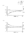
図3(a),(b)は本発明の実施の形態2におけるアルゴン発光強度と酸素発光強度との比と成膜レートの推移を示す特性図である。
【0041】
図3(a)に示すように真空チャンバー24の内部圧力を一定とした場合、波長697nmのアルゴン発光強度と酸素発光強度との比と成膜レートとの間に相関性がある。
【0042】
また、図3(b)に示すように成膜中に真空チャンバー24の内部圧力を変化させることによりアルゴン発光強度と酸素発光強度の比を一定とした場合、波長697nmのアルゴン発光強度と波長777nmの酸素発光強度の比と成膜レートの推移により成膜中のアルゴン発光強度と酸素発光強度の比を一定としたことにより、成膜レートが一定となっている。
【0043】
これは、図1に示すように、帰還制御ライン32から発光分光データの真空チャンバー24の圧力計27へのフィードバックにより実現されるものである。
【0044】
以上のように、成膜中に真空チャンバー24の圧力を変化させることによりアルゴン発光強度と酸素発光強度の比を一定にしたことにより、成膜レートが一定にできる。
【0045】
(実施の形態3)
実施の形態3について、図面を参照しながら説明する。
【0046】
実施の形態3において、実施の形態1と異なる点について説明する。
【0047】
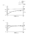
図4(a),(b)は本発明の実施の形態3におけるアルゴン発光強度と酸素発光強度との比と成膜レートの推移を示す特性図である。
【0048】
図4(a)に示すようにシース電位を一定とした場合、波長697nmのアルゴン発光強度と酸素発光強度との比と成膜レートとの間に相関性がある。
【0049】
また、図4(b)に示すように成膜中にシース電位を変化させることによりアルゴン発光強度と酸素発光強度の比を一定とした場合、波長697nmのアルゴン発光強度と波長777nmの酸素発光強度の比と成膜レートの推移により成膜中のアルゴン発光強度と酸素発光強度の比を一定にしたことにより、成膜レートが一定になっている。
【0050】
これは、図1に示すように、帰還制御ライン33から発光分光データの高周波マッチング回路30へのフィードバックにより実現されるものである。
【0051】
以上のように、成膜中のシース電位を変化させることによりアルゴン発光強度と酸素発光強度の比を一定にしたことにより、成膜レートが一定にできる。
【0052】
なお、プラズマ電位を変化させることによりアルゴン発光強度と酸素発光強度の比を一定にしたことにより、成膜レートが一定にできることはいうまでもない。
【0053】
(実施の形態4)
実施の形態4について、図面を参照しながら説明する。
【0054】
実施の形態4において、実施の形態1と異なる点について説明する。
【0055】
図5(a),(b)は本発明の実施の形態4におけるアルゴン発光強度と酸素発光強度との比と成膜レートの推移を示す特性図である。
【0056】
図5(a)に示すように高周波電力を一定とした場合、波長697nmのアルゴン発光強度と酸素発光強度との比と成膜レートとの間に相関性がある。
【0057】
また、図5(b)に示すように成膜中に高周波電力を変化させることによりアルゴン発光強度と酸素発光強度の比を一定とした場合、波長697nmのアルゴン発光強度と波長777nmの酸素発光強度の比と成膜レートの推移により成膜中のアルゴン発光強度と酸素発光強度の比を一定にしたことにより、成膜レートが一定となっている。
【0058】
これは、図1に示すように、帰還制御ライン34から発光分光データの高周波電源23へのフィードバックにより実現されるものである。
【0059】
以上のように、成膜中に高周波電力を変化させることによりアルゴン発光強度と酸素発光強度の比を一定にしたことにより、成膜レートが一定にできる。
【0060】
なお、DCスパッタリング装置を用いてスパッタリングを行う場合は、DC印加電圧を変化させてアルゴン発光強度と酸素発光強度の比を一定にすることで、成膜レートが一定にできる。
【0061】
(実施の形態5)
実施の形態5について、図面を参照しながら説明する。
【0062】
図6は本発明の実施の形態5におけるスパッタリング装置の概略を示す構成図である。
【0063】
図6において、21はスパッタターゲットであり、22は基板、23は高周波電源、24は真空チャンバー、25はプラズマモニター用の光ファイバー、26は分光器、27は圧力計、28はアルゴンガス流量計、29は酸素ガス流量計、30は高周波マッチング回路、35は光学式膜厚モニター用光ファイバー、36は光学式膜厚モニタリング手段である。
【0064】
実施の形態1で示したスパッタリング装置に光学式膜厚モニタリング手段36を設けて成膜中の波長697nmのアルゴン発光強度と波長777nmの酸素発光強度の比を一定にすることにより、一定の成膜レートを確認しながら成膜でき、深さ方向に均一な膜質をもつ薄膜を容易に得ることができる。
【0065】
なお、光学式膜厚モニタリング手段36は反射式のものを示したが、透過式を用いても同様の効果が得られる。
【0066】
【発明の効果】
以上のように本発明は、少なくともアルゴンガスと酸素を用いて基板上に薄膜を形成するスパッタリング方法において、プラズマ発光分光法を用いて前記アルゴンガスでは波長697nmの発光強度と、前記酸素では波長777nmの発光強度とが略等しく、かつその比が一定となるように前記アルゴンガスの流量または酸素流量を調整することで、前記薄膜の成膜レートを一定に制御するものであり、波長697nmのアルゴン発光強度と波長777nmの酸素発光強度とを用いて両者の波長および発光強度を近い値とすることにより、波長スパンおよびレベル分解能を高めることができるので高精度に評価することができ、その結果、成膜レートを一定に制御して高精度の膜厚制御を実現できる。
【図面の簡単な説明】
【図1】本発明の実施の形態1におけるスパッタリング装置の断面図
【図2】(a),(b)本発明の実施の形態1におけるアルゴン発光強度と酸素発光強度の比と成膜レートの推移を示す特性図
【図3】(a),(b)本発明の実施の形態2におけるアルゴン発光強度と酸素発光強度の比と成膜レートの推移を示す特性図
【図4】(a),(b)本発明の実施の形態3におけるアルゴン発光強度と酸素発光強度の比と成膜レートの推移を示す特性図
【図5】(a),(b)本発明の実施の形態4におけるアルゴン発光強度と酸素発光強度の比と成膜レートの推移を示す特性図
【図6】本発明の実施の形態5におけるスパッタリング装置の概略を示す構成図
【図7】従来のスパッタリング装置の構成を示すブロック図
【符号の説明】
21 スパッタターゲット
22 基板
23 高周波電源
24 真空チャンバー
25 光ファイバー
26 分光器
27 圧力計
28 アルゴンガス流量計
29 酸素ガス流量計
30 高周波マッチング回路
31 帰還制御ライン
32 帰還制御ライン
33 帰還制御ライン
34 帰還制御ライン
35 光ファイバー
36 光学式膜厚モニタリング手段[0001]
BACKGROUND OF THE INVENTION
The present invention mainly relates to a sputtering method and a sputtering apparatus for forming a thin film such as a predetermined multilayer optical thin film or oxide thin film with good reproducibility on the surface of a glass substrate.
[0002]
[Prior art]
FIG. 7 shows a conventional sputtering method and sputtering apparatus.
[0003]
FIG. 7 is a block diagram showing an apparatus for forming a multilayer optical thin film by a conventional sputtering method.
[0004]
1 is an apparatus for measuring the optical characteristics of a thin film, 2 is a load lock chamber, 3 is a film forming chamber, 4 is a sputter target, 5 is a rotating member to which a plurality of sputter targets 4 are attached, and 5a is a rotating
[0005]
Further, in the method of forming a multilayer optical thin film on the surface of the substrate, the multilayer optical thin film was formed based on the film thickness setting value of each layer, and the optical characteristics of the formed multilayer optical thin film were measured. Obtain the film thickness of each layer so that the multilayer optical thin film has the target optical characteristic based on the optical characteristics, correct the film thickness setting value based on the obtained film thickness of each layer, and correct this film thickness setting The next multilayer optical thin film is formed based on the value. Alternatively, in the method of forming a thin film by sputtering, H 2 O gas concentration or discharge impedance in a vacuum chamber is measured, and at least one of sputtering power, sputtering gas partial pressure, and sputtering gas flow rate is measured according to the measurement result. The above is controlled so that the sputtering rate is kept constant.
[0006]
For example,
[0007]
[Patent Document 1]
Japanese Patent Laid-Open No. 7-72307
[Problems to be solved by the invention]
However, since the conventional configuration employs an indirect method of using H 2 O molecules that are not in a plasma state in the apparatus, the film formation rate may change. It is not fully explained about the event.
[0009]
That is, quantitative information about H 2 O molecules is described, but it is not described at all in quantitative information, verification data, etc. about H radicals, H + ions, H − ions or oxygen atoms. In addition, since an indirect method is used, there is a problem in realizing high accuracy.
[0010]
An object of this invention is to provide the sputtering method and sputtering apparatus which can implement | achieve highly accurate film thickness measurement and can implement | achieve highly accurate film thickness control.
[0011]
[Means for Solving the Problems]
The invention according to
[0019]
DETAILED DESCRIPTION OF THE INVENTION
Hereinafter, embodiments of the present invention will be described with reference to the drawings.
[0020]
(Embodiment 1)
FIG. 1 is a configuration diagram showing an outline of a sputtering apparatus according to
[0021]
In FIG. 1, 21 is a sputter target, 22 is a substrate, 23 is a high frequency power source, 24 is a vacuum chamber, 25 is an optical fiber for plasma monitoring, 26 is a spectroscope, 27 is a pressure gauge, 28 is an argon gas flow meter, 29 is An oxygen gas flow meter, 30 is a high-frequency matching circuit, and 31 to 34 are feedback control lines.
[0022]
In the sputtering apparatus of the present invention, power is supplied from a high
[0023]
A
[0024]
Hereinafter, the thin film forming method will be described.
[0025]
A support (not shown) provided with the
[0026]
For example, the deposition conditions for Ta 2 O 5 are shown in Table 1.
[0027]
[Table 1]
Moreover, the
[0029]
(Table 1) By performing film formation under the conditions that the high frequency power is 1000 W, the argon gas flow rate is 10 sccm, the oxygen gas flow rate is 0.4 sccm, and the internal pressure of the
[0030]
In addition, the measurement wavelength of the refractive index at this time is 632.8 nm.
[0031]
FIGS. 2A and 2B are characteristic diagrams showing the transition of the film formation rate and the ratio of the argon emission intensity to the oxygen emission intensity in
[0032]
As shown in FIG. 2A, the ratio of the argon emission intensity at a wavelength of 697 nm and the oxygen emission intensity at a wavelength of 777 nm during film formation and the transition of the film formation rate correlate with the ratio of the argon light emission intensity and the oxygen emission intensity and the film formation rate. There is sex.
[0033]
As shown in FIG. 2B, when the ratio of the argon emission intensity and the oxygen emission intensity is made constant by changing the argon gas flow rate during film formation, the argon emission intensity at a wavelength of 697 nm and the oxygen emission intensity at a wavelength of 777 nm are obtained. By making the ratio of the argon emission intensity and the oxygen emission intensity during film formation constant from the transition of the ratio and the film formation rate, the film formation rate becomes constant.
[0034]
As shown in FIG. 1, this is realized by feedback of the emission spectral data from the
[0035]
As described above, the film formation rate can be made constant by changing the argon gas flow rate during film formation to make the ratio of the argon emission intensity and the oxygen emission intensity constant.
[0036]
Needless to say, the film formation rate can be made constant by changing the flow rate of the oxygen gas to make the ratio of the argon emission intensity and the oxygen emission intensity constant.
[0037]
Moreover, the
[0038]
(Embodiment 2)
The second embodiment will be described with reference to the drawings.
[0039]
The second embodiment will be described with respect to differences from the first embodiment.
[0040]
FIGS. 3A and 3B are characteristic diagrams showing the transition of the film formation rate and the ratio between the argon emission intensity and the oxygen emission intensity in the second embodiment of the present invention.
[0041]
As shown in FIG. 3A, when the internal pressure of the
[0042]
Further, as shown in FIG. 3B, when the ratio of the argon emission intensity and the oxygen emission intensity is made constant by changing the internal pressure of the
[0043]
As shown in FIG. 1, this is realized by feedback of the emission spectral data from the
[0044]
As described above, the film formation rate can be made constant by changing the pressure of the
[0045]
(Embodiment 3)
The third embodiment will be described with reference to the drawings.
[0046]
In the third embodiment, differences from the first embodiment will be described.
[0047]
4 (a) and 4 (b) are characteristic diagrams showing changes in the ratio between the argon emission intensity and the oxygen emission intensity and the film formation rate in Embodiment 3 of the present invention.
[0048]
When the sheath potential is constant as shown in FIG. 4A, there is a correlation between the ratio of the argon emission intensity and the oxygen emission intensity at a wavelength of 697 nm and the film formation rate.
[0049]
Further, as shown in FIG. 4B, when the ratio of the argon emission intensity and the oxygen emission intensity is made constant by changing the sheath potential during film formation, the argon emission intensity at a wavelength of 697 nm and the oxygen emission intensity at a wavelength of 777 nm. By making the ratio of the argon emission intensity and the oxygen emission intensity during film formation constant by the change of the ratio and the film formation rate, the film formation rate is constant.
[0050]
As shown in FIG. 1, this is realized by feedback from the
[0051]
As described above, the film formation rate can be made constant by changing the sheath potential during film formation to make the ratio of the argon emission intensity and the oxygen emission intensity constant.
[0052]
Needless to say, the film formation rate can be made constant by changing the plasma potential to make the ratio of the argon emission intensity and the oxygen emission intensity constant.
[0053]
(Embodiment 4)
The fourth embodiment will be described with reference to the drawings.
[0054]
In the fourth embodiment, differences from the first embodiment will be described.
[0055]
FIGS. 5A and 5B are characteristic diagrams showing the transition of the film formation rate and the ratio of the argon emission intensity to the oxygen emission intensity in the fourth embodiment of the present invention.
[0056]
When the high frequency power is constant as shown in FIG. 5A, there is a correlation between the ratio of the argon emission intensity and the oxygen emission intensity at a wavelength of 697 nm and the film formation rate.
[0057]
Further, as shown in FIG. 5B, when the ratio of the argon emission intensity and the oxygen emission intensity is made constant by changing the high frequency power during film formation, the argon emission intensity at a wavelength of 697 nm and the oxygen emission intensity at a wavelength of 777 nm. By making the ratio of the argon emission intensity and the oxygen emission intensity during film formation constant by changing the ratio of the above and the film formation rate, the film formation rate is constant.
[0058]
As shown in FIG. 1, this is realized by feedback of the emission spectral data from the
[0059]
As described above, the film formation rate can be made constant by making the ratio of the argon emission intensity and the oxygen emission intensity constant by changing the high frequency power during the film formation.
[0060]
Note that when sputtering is performed using a DC sputtering apparatus, the film formation rate can be made constant by changing the DC applied voltage to make the ratio of the argon emission intensity and the oxygen emission intensity constant.
[0061]
(Embodiment 5)
A fifth embodiment will be described with reference to the drawings.
[0062]
FIG. 6 is a configuration diagram showing an outline of a sputtering apparatus according to
[0063]
In FIG. 6, 21 is a sputter target, 22 is a substrate, 23 is a high frequency power source, 24 is a vacuum chamber, 25 is an optical fiber for plasma monitoring, 26 is a spectroscope, 27 is a pressure gauge, 28 is an argon gas flow meter, 29 is an oxygen gas flow meter, 30 is a high frequency matching circuit, 35 is an optical film thickness monitoring optical fiber, and 36 is an optical film thickness monitoring means.
[0064]
The optical film thickness monitoring means 36 is provided in the sputtering apparatus shown in the first embodiment, and the ratio of the argon emission intensity at a wavelength of 697 nm and the oxygen emission intensity at a wavelength of 777 nm during film formation is made constant, thereby forming a constant film formation. A film can be formed while checking the rate, and a thin film having a uniform film quality in the depth direction can be easily obtained.
[0065]
The optical film thickness monitoring means 36 is a reflection type, but the same effect can be obtained by using a transmission type.
[0066]
【The invention's effect】
As described above, according to the present invention, in a sputtering method for forming a thin film on a substrate using at least argon gas and oxygen, the emission intensity at a wavelength of 697 nm with the argon gas and the wavelength at 777 nm with oxygen are measured using plasma emission spectroscopy. The film formation rate of the thin film is controlled to be constant by adjusting the flow rate of the argon gas or the oxygen flow rate so that the emission intensity is substantially equal and the ratio is constant, and the argon film has a wavelength of 697 nm. By using the emission intensity and the oxygen emission intensity at a wavelength of 777 nm to make the wavelength and emission intensity close to each other, the wavelength span and level resolution can be increased, so that it can be evaluated with high accuracy. High-precision film thickness control can be realized by controlling the film formation rate to be constant.
[Brief description of the drawings]
FIGS. 1A and 1B are cross-sectional views of a sputtering apparatus according to
21
Claims (1)
Priority Applications (1)
| Application Number | Priority Date | Filing Date | Title |
|---|---|---|---|
| JP2003080273A JP4457566B2 (en) | 2003-03-24 | 2003-03-24 | Sputtering method |
Applications Claiming Priority (1)
| Application Number | Priority Date | Filing Date | Title |
|---|---|---|---|
| JP2003080273A JP4457566B2 (en) | 2003-03-24 | 2003-03-24 | Sputtering method |
Publications (2)
| Publication Number | Publication Date |
|---|---|
| JP2004285431A JP2004285431A (en) | 2004-10-14 |
| JP4457566B2 true JP4457566B2 (en) | 2010-04-28 |
Family
ID=33294178
Family Applications (1)
| Application Number | Title | Priority Date | Filing Date |
|---|---|---|---|
| JP2003080273A Expired - Fee Related JP4457566B2 (en) | 2003-03-24 | 2003-03-24 | Sputtering method |
Country Status (1)
| Country | Link |
|---|---|
| JP (1) | JP4457566B2 (en) |
Families Citing this family (1)
| Publication number | Priority date | Publication date | Assignee | Title |
|---|---|---|---|---|
| JP2008121034A (en) * | 2006-11-08 | 2008-05-29 | Kochi Prefecture Sangyo Shinko Center | Method and apparatus for forming a zinc oxide thin film |
Family Cites Families (5)
| Publication number | Priority date | Publication date | Assignee | Title |
|---|---|---|---|---|
| JPS6477940A (en) * | 1987-09-19 | 1989-03-23 | Fujitsu Ltd | Plasma processing |
| JP2584058B2 (en) * | 1989-05-26 | 1997-02-19 | 松下電器産業株式会社 | Transparent conductive film forming apparatus and transparent conductive film forming method |
| JP2905342B2 (en) * | 1992-09-07 | 1999-06-14 | 財団法人国際超電導産業技術研究センター | Method for producing YBa2Cu3Ox superconducting thin film |
| JPH0772307A (en) * | 1993-09-03 | 1995-03-17 | Canon Inc | Thin film forming method and apparatus |
| JP4339437B2 (en) * | 1999-03-31 | 2009-10-07 | 大日本印刷株式会社 | Vacuum deposition system |
-
2003
- 2003-03-24 JP JP2003080273A patent/JP4457566B2/en not_active Expired - Fee Related
Also Published As
| Publication number | Publication date |
|---|---|
| JP2004285431A (en) | 2004-10-14 |
Similar Documents
| Publication | Publication Date | Title |
|---|---|---|
| US6863785B2 (en) | Sputtering apparatus and sputter film deposition method | |
| JP4818073B2 (en) | Film thickness measurement method | |
| JPH0770749A (en) | Thin film forming method and apparatus | |
| TW503405B (en) | Method of manufacturing substrate having transparent conductive film, substrate having transparent conductive film manufactured using the method, and touch panel using the substrate | |
| JPH0772307A (en) | Thin film forming method and apparatus | |
| JP4530776B2 (en) | Multilayer film forming sputtering apparatus and film thickness control method thereof | |
| JP4457566B2 (en) | Sputtering method | |
| JP2637509B2 (en) | Novel diamond-like carbon film and method for producing the same | |
| WO2023223845A1 (en) | Film thickness measurement method and substrate processing device | |
| JP4487264B2 (en) | Sputtering apparatus and sputter deposition method | |
| JP2002339084A (en) | Metal film and metal film coated member | |
| JP2009228062A (en) | Sputtering film deposition apparatus and sputtering film deposition method | |
| JPH04212414A (en) | Plasma process equipment | |
| JP2001240965A (en) | Method and apparatus for controlling film thickness distribution in thin film manufacturing apparatus | |
| JP4693554B2 (en) | Temperature measuring apparatus and temperature measuring method | |
| JP3892961B2 (en) | Optical thin film manufacturing method | |
| JP4830260B2 (en) | Film thickness detection method | |
| JPH08172054A (en) | Plasma CVD method, apparatus therefor, and method of manufacturing semiconductor device using the same | |
| CN118581436B (en) | A method for intelligently adjusting the coating position of a glass substrate | |
| JP2002170812A (en) | Method and apparatus for detecting end point of plasma etching and plasma etching apparatus | |
| Schwaller et al. | Rapid depth profiling of lead zirconate titanate (PZT) thin films by pulsed glow‐discharge optical emission spectroscopy | |
| JPS596376A (en) | Sputtering apparatus | |
| JPH0370326B2 (en) | ||
| JP2004320759A (en) | Layer stack deposition method, resonator formation method, piezoelectric layer deposition method, and resonator | |
| JP3528930B2 (en) | Method for manufacturing transparent conductive film |
Legal Events
| Date | Code | Title | Description |
|---|---|---|---|
| A621 | Written request for application examination |
Free format text: JAPANESE INTERMEDIATE CODE: A621 Effective date: 20051214 |
|
| RD01 | Notification of change of attorney |
Free format text: JAPANESE INTERMEDIATE CODE: A7421 Effective date: 20060112 |
|
| A977 | Report on retrieval |
Free format text: JAPANESE INTERMEDIATE CODE: A971007 Effective date: 20080702 |
|
| A131 | Notification of reasons for refusal |
Free format text: JAPANESE INTERMEDIATE CODE: A131 Effective date: 20080708 |
|
| A521 | Written amendment |
Free format text: JAPANESE INTERMEDIATE CODE: A523 Effective date: 20080905 |
|
| A131 | Notification of reasons for refusal |
Free format text: JAPANESE INTERMEDIATE CODE: A131 Effective date: 20090929 |
|
| RD01 | Notification of change of attorney |
Free format text: JAPANESE INTERMEDIATE CODE: A7421 Effective date: 20091119 |
|
| A521 | Written amendment |
Free format text: JAPANESE INTERMEDIATE CODE: A523 Effective date: 20091127 |
|
| TRDD | Decision of grant or rejection written | ||
| A01 | Written decision to grant a patent or to grant a registration (utility model) |
Free format text: JAPANESE INTERMEDIATE CODE: A01 Effective date: 20100119 |
|
| A01 | Written decision to grant a patent or to grant a registration (utility model) |
Free format text: JAPANESE INTERMEDIATE CODE: A01 |
|
| A61 | First payment of annual fees (during grant procedure) |
Free format text: JAPANESE INTERMEDIATE CODE: A61 Effective date: 20100201 |
|
| FPAY | Renewal fee payment (event date is renewal date of database) |
Free format text: PAYMENT UNTIL: 20130219 Year of fee payment: 3 |
|
| FPAY | Renewal fee payment (event date is renewal date of database) |
Free format text: PAYMENT UNTIL: 20130219 Year of fee payment: 3 |
|
| FPAY | Renewal fee payment (event date is renewal date of database) |
Free format text: PAYMENT UNTIL: 20140219 Year of fee payment: 4 |
|
| LAPS | Cancellation because of no payment of annual fees |