JP4457549B2 - Nitride semiconductor laser device and manufacturing method thereof - Google Patents
Nitride semiconductor laser device and manufacturing method thereof Download PDFInfo
- Publication number
- JP4457549B2 JP4457549B2 JP2002297129A JP2002297129A JP4457549B2 JP 4457549 B2 JP4457549 B2 JP 4457549B2 JP 2002297129 A JP2002297129 A JP 2002297129A JP 2002297129 A JP2002297129 A JP 2002297129A JP 4457549 B2 JP4457549 B2 JP 4457549B2
- Authority
- JP
- Japan
- Prior art keywords
- layer
- nitride semiconductor
- semiconductor layer
- semiconductor laser
- window region
- Prior art date
- Legal status (The legal status is an assumption and is not a legal conclusion. Google has not performed a legal analysis and makes no representation as to the accuracy of the status listed.)
- Expired - Fee Related
Links
Images

Landscapes
- Semiconductor Lasers (AREA)
Description
【0001】
【発明の属する技術分野】
本発明はストライプ状の導波路領域を有する窒化物半導体レーザ素子に係り、端面にウインドウ構造を有し、高出力が可能な窒化物半導体レーザ素子であって、特に、共振器面に窒化物半導体が再成長されてなる端面成長型ウインドウ構造に関するものである。本発明の窒化物半導体レーザ素子に用いる具体的な組成としては、GaN、AlN、若しくはInN、又はこれらの混晶であるIII−V族窒化物半導体(InxAlyGa1−x−yN、0≦x、0≦y、x+y≦1)を用いた窒化物半導体レーザ素子が挙げられる。
【0002】
【従来の技術】
近年、半導体レーザは、小型、長寿命、高信頼性、かつ高出力化が進み、主にパーソナルコンピュータ、DVDなどの電子機器、医療機器、加工機器や光ファイバ通信の光源などに利用されている。中でも窒化物半導体(InxAlyGa1−x−yN、0≦x、0≦y、x+y≦1)は、比較的短波長の紫外域から赤色が発光可能な半導体レーザとして注目されている。
【0003】
窒化物半導体レーザ素子は、サファイア基板上にバッファ層、n型コンタクト層、クラック防止層、n型クラッド層、n型光ガイド層、活性層、p型光ガイド層、p型キャップ層、p型クラッド層、p型コンタクト層などが順に積層された積層構造体からなっている。そして、このような積層構造体にリッジストライプが形成されることでストライプ状の導波路領域が設けられ、その導波路領域の端面に共振器面が形成されている。
【0004】
このような窒化物半導体レーザ素子では、劈開により共振器面を形成させるのが必ずしも容易ではないため、エッチングにより共振器面を形成することが検討されている。エッチングの方法としては、異方性エッチングが可能な反応性イオンエッチング(RIE)等のドライエッチングが好ましく用いられている。このようなRIEによって形成されたエッチング面は劈開面に比べると凹凸が多いため、反射損失が大きくなる。そのような問題を解決する技術として、共振器面に誘電体保護膜等を設けてその損失を補うことができる。しかしながら、このような誘電体保護膜を設けたとしても、高出力時に充分耐えうるものではない。このような問題を解決するために、活性層よりもバンドギャップの広い保護膜(ウインドウ領域)を設けるという技術がある。ウインドウ領域を設けることで、端面の劣化を抑制することができる。
【0005】
【特許文献1】
特開平07−249830号公報
【0006】
【発明が解決しようとする課題】
ところが、ウインドウ領域が導波路領域近傍だけでなく、端面の広い領域に形成されていると、活性層からの光がウインドウ領域内を伝搬してしまい、光損失が多くなるという問題が生じる場合がある。また、ウインドウ領域の製造方法においては、エッチングによる共振器面が半導体層の成長面と略垂直な方向であるため、ウエハのまま成長させると、均一な膜質のウインドウ領域が得られにくいという問題がある。更に、ウインドウ領域成長時に、その成長温度によって素子特性が劣化するという問題も生じる。そこで、本発明は上記問題を鑑み、ウインドウ領域による光損失の少ない窒化物半導体レーザ素子を提供することを目的とする。また、均一な膜質のウインドウ領域が得られ、また、ウインドウ領域形成時の素子特性劣化を抑制する窒化物半導体レーザ素子の製造方法を提供することを目的とする。
【0007】
【課題を解決するための手段】
本発明における窒化物半導体レーザ素子は、基板上に形成されたn型半導体層、活性層、及びp型半導体層からなる窒化物半導体層にリッジストライプからなる導波路領域を有し、導波路領域の共振器面に活性層よりもバンドギャップの広い窒化物半導体からなるウインドウ領域を有する窒化物半導体レーザ素子であって、窒化物半導体層は、一部が共振器面よりも突出するn型半導体層突出部を有し、ウインドウ領域は、p型半導体層の端面から、n型半導体層突出部より活性層側のn型半導体層の端面までの端面領域に形成され、前記基板の表面は、n型半導体層突出部から露出することを特徴とする。
【0008】
本発明の請求項2に記載の窒化物半導体レーザ素子は、ウインドウ領域は、共振器面での膜厚が、n型半導体層突出部の端面から前記共振器面までの距離よりも小さいことを特徴とする。
【0009】
本発明の請求項3に記載の窒化物半導体レーザ素子は、ウインドウ領域は、導波路領域から離間する領域が遮光膜で被覆されていることを特徴とする。
【0010】
本発明の請求項4に記載の窒化物半導体レーザ素子は、n型半導体層突出部は、端面が遮光膜で被覆されていることを特徴とする。
【0011】
本発明の請求項5に記載の窒化物半導体レーザ素子は、活性層はInxGa1−xN(0≦x≦1)を含む層であり、ウインドウ領域はAlyGa1−yN(0≦y≦1)からなることを特徴とする。
【0013】
本発明の請求項6に記載の窒化物半導体レーザ素子の製造方法は、基板上に、n型半導体層、活性層、及びp型半導体層からなる窒化物半導体層を積層後、エッチングによって共振器面を形成し、共振器面に、活性層よりもバンドギャップの広い窒化物半導体からなるウインドウ領域を形成する窒化物半導体レーザ素子の製造方法であって、前記ウインドウ領域形成後に、対向する共振器面の間の半導体層を更にエッチングして、共振器面から突出するn型半導体層突出部を形成する工程を有し、前記n型半導体層突出部から露出した領域において素子分割を行うことを特徴とする。
本発明の請求項7に記載の窒化物半導体レーザ素子の製造方法は、前記ウインドウ領域は、前記p型半導体層の上面に表面保護膜を形成し、その表面保護膜を有したまま形成させることを特徴とする。
【0014】
本発明の請求項8に記載の窒化物半導体レーザ素子の製造方法は、ウインドウ領域を形成後に、リッジストライプを形成することを特徴とする。
【0016】
本発明の請求項9に記載の窒化物半導体レーザ素子は、共振器面は、窒化物半導体のM面であることを特徴とする。
【0017】
本発明の請求項10に記載の窒化物半導体レーザ素子の製造方法は、表面保護膜は、共振器面形成時のエッチングマスクであることを特徴とする。
【0018】
本発明の請求項11に記載の窒化物半導体レーザ素子の製造方法は、表面保護膜は、エッチングマスクと窒化物半導体層との間に、第1の保護膜を有することを特徴とする。
【0019】
本発明の請求項12に記載の窒化物半導体レーザ素子の製造方法は、第1の保護膜は、エッチングマスクと同等又はそれより大きく形成されていることを特徴とする。
【0020】
本発明の請求項13に記載の窒化物半導体レーザ素子の製造方法は、第1の保護膜は、窒化物半導体であることを特徴とする。
【0021】
本発明の請求項14に記載の窒化物半導体レーザ素子の製造方法は、第1の保護膜は、AlNであることを特徴とする。
【0022】
本発明の請求項15に記載の窒化物半導体レーザ素子の製造方法は、エッチングマスクは、SiO2を含む化合物であることを特徴とする。
本発明の請求項16に記載の窒化物半導体レーザ素子の製造方法は、前記n型半導体層突出部を形成する工程は、基板が露出するまでエッチングすることを特徴とする。
【0023】
【発明の実施の形態】
本発明に係る実施の形態の窒化物半導体レーザ素子は、n型半導体層、活性層、及びp型半導体層からなる窒化物半導体層からなっている。p型半導体層にはリッジストライプが形成されており、これによりストライプ状の実効屈折率型の導波路領域が設けられる。そして、ストライプ状導波路領域と直交するように設けられている共振器面に、活性層よりもバンドギャップの広い半導体層からなるウインドウ領域を有しているものである。
【0024】
本実施の形態の窒化物半導体レーザ素子は、図1に示すように共振器面よりも突出するn型半導体層突出部15を有するものであり、p型半導体層の端面からn型半導体層突出部より活性層側のn型半導体層の端面までの端面領域に、ウインドウ領域9が形成されていることを特徴とするものである。
【0025】
(ウインドウ領域)
p型半導体層まで成長させた窒化物半導体層に共振器面を形成すると、その共振器面には表面準位が存在する。素子駆動時にはその表面準位が非発光性再結合を促進して熱が発生し、この熱の発生により共振器面のバンドギャップが小さくなるという現象が生じる。バンドギャップが小さくなると光を吸収しやすくなるので、これにより、更に共振器面の温度上昇が加速されてバンドギャップが小さくなる、というサイクルが生じる。このような現象により、ついには共振器面が融解してCODが生じる。ウインドウ領域はこのような現象を抑制するためのもので、共振器面に活性層よりもバンドギャップの広い窒化物半導体を設けることで、バンドギャップが小さくなることによる光の吸収を抑制することができる。
【0026】
本実施の形態の窒化物半導体レーザ素子は、上記のようなウインドウ領域を、端面全面ではなく、活性層を含む導波路領域近傍に形成させるものである。具体的には、共振器面形成時のエッチングをn型半導体層の一部が露出する深さまでとし、共振器面と同一平面領域を少なくし、その領域にウインドウ領域を形成させるものである。ウインドウ領域は、上述のように、活性層よりもバンドギャップの広い窒化物半導体層であるので、光の吸収は少ない層ではあるが、光の伝搬は可能な層である。従って、外部との屈折率差、及び窒化物半導体層との界面との屈折率差によってウインドウ領域内を光が反射しながら伝搬することが可能であるので、活性層を含む導波路領域から出射された光はウインドウ領域全般に伝搬されることになる。本実施の形態の窒化物半導体レーザ素子は、このようなウインドウ領域の形成面積を小さくすることで、光の伝搬する領域を少なくすることができる。これにより、導波路領域から離れた位置にまで光が伝搬して出射面以外から光が放出されることによるFFPの乱れなどを生じにくくすることができる。すなわち、ウインドウ領域の形成面積を小さくすることで、ウインドウ領域によるビーム特性の悪化の少ない窒化物半導体レーザ素子とすることができる。
【0027】
ウインドウ領域の大きさは、n型半導体層突出部の形成位置によって適宜選択することができる。少なくとも活性層の端面に形成させることが必要であり、光ガイド層を有する場合などは、その層も含めた導波路領域の端面に形成させる必要がある。ガイド層よりも外側の層、例えばクラッド層の端面については、光の吸収を抑制するという意味では特に設けなくてもよいが、設けないことで共振器面近傍の屈折率差が大きくなってビーム特性に悪影響を及ぼす場合があるので、設けるのが好ましい。コンタクト層については、n型コンタクト層は導波路領域からの距離が大きいので特に設ける必要はないが、p型コンタクト層はn型コンタクト層に比べて活性層に近く、その膜厚も薄いため、設けるのが好ましい。
【0028】
また、ウインドウ領域の膜厚は、共振器面からの膜厚が100Å〜10μmの範囲が好ましく、より好ましくは1000Å〜1μmであり、更に好ましくは400Å〜7000Åである。ウインドウ領域の膜厚が100Åより小さいと、ウインドウ領域として機能しにくくなるので好ましくない。また、10μmよりも大きくなると、光学特性を悪化させるので好ましくない。また、n型半導体層突出部の端部よりも突出しないようにするのが好ましく、より好ましくは、共振器面から離間するn型半導体層突出部の上部には設けないようにするのが好ましい。
【0029】
本実施の形態において、窒化物半導体レーザ素子の活性層は、InxGa1−xN(0≦x≦1)を含む層で有る場合、ウインドウ領域はAlyGa1−yN(0≦y≦1)とするのが好ましい。活性層は、Inを含むものとすることで可視〜紫外領域までの広い波長範囲の発光が可能な窒化物半導体レーザ素子とすることができる。そして、このような活性層よりもバンドギャップを広くするために、上記組成からなるウインドウ領域を形成させるのが好ましい。上記組成式でx及びyを0以外とすることで、組成の異なるものとすることが可能であり、このような組成の組み合わせによりバンドギャップを変更するのが好ましい。また、上記組成において、xとyを共に0とすることで活性層とウインドウ領域とが同じ組成となるが、例え同じ組成であっても、成長条件や膜厚等によってはバンドギャップを変更することができるので、組成変更が困難な場合は同一の組成とすることもできる。
【0030】
(n型半導体層突出部)
本実施の形態の窒化物半導体レーザ素子は、ウインドウ領域を導波路領域近傍の限られた領域に設けるために、n型半導体層の端面が一部突出するよう形状を有している。このような端面形状とすることで、マスク材等を用いることなくウインドウ領域の形成領域を小さくすることが容易になる。特に、ウエハのままで共振器面を含む端面の一部に再成長のためのマスクを設けることは困難であり、例え形成できたとしても制御よく形成しにくく、そのマスクの膜質も充分なものが得られにくい。そのため、ウインドウ領域の膜質が不十分なものなりやすい。本実施の形態のような端面形状とすることで、均一な膜質の半導体からなるウインドウ領域を得ることができる。
【0031】
n型半導体層突出部に含まれるn型半導体層は、共振器面形成時のエッチング深さによって制御することができる。例えば、共振器面形成時に、n型コンタクト層の途中までエッチングすると、n型半導体層突出部はn型コンタクト層の一部と下地層やバッファ層などとすることができる。また、n型半導体層側に基板を有する場合は、基板もn型半導体層突出部の一部とみなしてよい。
【0032】
また、上述のように、n型半導体層突出部の端面から共振器面までの距離は、ウインドウ領域の共振器面での膜厚よりも大きくするのが好ましい。これにより、n型半導体層突出部の方がウインドウ領域よりも突出していることになるので、後の工程でウインドウ領域を劈開或いはエッチング等で加工せずに用いることができる。すなわち共振器面への半導体の再成長によって形成されている、ウインドウ領域を、その成長面をそのまま出射面として用いることができることで、光の損失を極めて少なくすることができる。但し、n型半導体層突出部がウインドウ領域よりもあまり突出しすぎると、導波路領域から出射される光がn型半導体層突出部によって遮られてビーム形状が悪化することになるので、出射光を遮らない程度にする必要がある。
【0033】
(遮光膜)
先に述べたように、ウインドウ領域は光の吸収しにくい層であって、活性層からの光は、素子内部と同様に伝搬される層である。従って、共振器面から出射された光はウインドウ領域内を伝搬して任意の位置から外部に放出されることになる。そのような光がレーザ光の主ビームに混ざることで光分布に凹凸(リップル)が生じ、FFPが悪化する。このような現象を改善するために、ウインドウ領域の表面のうち、導波路領域から離間した部分を遮光膜で被覆することができる。このように、リッジストライプから離間した活性層端面を含む端面に遮光膜を設けることで、FFPのx成分に生じるリップルを低減させることができる。この遮光膜は、活性層からの光を遮光することが可能なものであればよく、例えば、Ni、Cr、Ti、Cu、Fe、Zr、Hf、Nb、W、Rh、Ru、Mg、Ga、Pt、Au、Si、Pd、V、Ta、Mo、C等を用いた材料を選択することができる。より好ましくは、Ni、Cr、Ti、Siを用いた材料である。また、これらの酸化物等も用いることができる。以上の材料は単層膜で用いることもできるし、或いは多層膜として用いることもできる。
【0034】
次に、本発明の窒化物半導体レーザ素子の各層及び構成について詳説する。
(窒化物半導体)
本発明の窒化物半導体レーザ素子として用いられる半導体層としては、GaN、AlN、InN、及びこれらの混晶であるIII−V族窒化物半導体(InxAlyGa1−x−yN、0≦x、0≦y、x+y≦1)が好ましい。以下、本発明の窒化物半導体レーザ素子について具体的に説明する。
【0035】
(成長基板)
成長基板としては、窒化物半導体層をエピタキシャル成長させることができる基板であれば異種基板でも同種基板でもよく、大きさや厚さ等は特に限定されない。具体的な例としては、異種基板では、C面、R面、及びA面のいずれかを主面とするサファイアやスピネル(MgA12O4)のような絶縁性基板、また炭化珪素(6H、4H、3C)、シリコン、ZnS、ZnO、Si、GaAs、ダイヤモンド、及び窒化物半導体と格子接合するニオブ酸リチウム、ガリウム酸ネオジウム等の酸化物基板が挙げられる。また、デバイス加工が出来る程度の厚膜(数十μm以上)であれば同種基板である窒化物半導体基板を用いることもできる。
【0036】
成長基板として異種基板を用いる場合は、窒化物半導体層を成長させる前にバッファ層を成長させるのが好ましい。バッファ層としては、一般式AlaGa1−aN(0≦a≦0.8)で表される窒化物半導体、より好ましくは、AlaGa1−aN(0.05≦a≦0.5)で示される窒化物半導体を用いる。バッファ層の成長温度としては、低温成長であるのが好ましい。これにより、窒化物半導体層上の転位やピットを低減させることができる。さらに、前記異種基板上にELO(Epitaxial−Lateral−Overgrowth)法によりAlxGa1−xN(0≦X≦1)層を成長させてもよい。又は、基板上に横方向成長させた窒化物半導体をT字形状とし、保護膜を除去させた後、さらに窒化物半導体を再成長させたものを用いてもよい。このような窒化物半導体層を有する異種基板は、T字柱上には転位が伸びるものの、T字両翼上部、及び隣り合うT字両翼の開口部上には転位が大幅に低減された結晶性の良好な窒化物半導体基板を得ることができ、再成長させた接合部にも転位が低減するため、この基板は低欠陥領域がウエハ上に広範囲で存在することとなる。そのため、この基板上に形成した窒化物半導体レーザ素子は寿命特性の良好なものが期待できる。またT字両翼下には保護膜除去により再成長後も空洞が残るため、反り抑制効果もある。
【0037】
また、上記のような窒化物半導体層の成長基板として用いることはできないが、レーザ素子として駆動させる時に半導体層を保持するために、成長基板とは異なる基板(支持基板)を設けることもできる。例えば、成長基板が絶縁性の基板である場合に、支持基板として金属などからなる導電性の基板を用いることができる。このような導電性の支持基板を用いると、半導体層の上下面に電極を設けることができるので、素子内部の抵抗を低減させることができる。すなわち、成長基板の特性(例えば絶縁性)が、素子駆動時の弊害(同一面側に両電極形成)となっている場合には、成長基板をそのまま保持するのではなく、別の材質からなる支持基板に接合させることで、より優れた特性を得ることができる。このような支持基板は、p型半導体側でもn側半導体層側でもよく、支持基板の材料についても、適宜選択することができる。また、成長基板の分離、支持基板の接合等の工程は、ウインドウ領域形成の前或いは後に行うことができる。
【0038】
(活性層)
本発明の窒化物半導体レーザ素子は、特に活性層がInを含む窒化物半導体層を有するものが好ましい。これにより、紫外線及び可視域において紫色系から赤色系の波長のレーザ光を得ることができる。また、活性層は、量子井戸構造であってもよく、その場合、単一量子井戸、多量子井戸のいずれでも良い。好ましくは量子井戸構造とすることで、発光効率に優れ、高出力のレーザ素子が得られる。具体的には、AlxInyGa1−x−yN(0≦x≦1、0<y≦1、x+y≦1)で表される窒化物半導体を用いることが好ましい。この場合、量子井戸構造の活性層においては、井戸層としてここで示した窒化物半導体を用いることが好ましいことを意味する。また、近紫外から可視光の緑色までの波長領域(380nm以上550nm以下)では、InyGa1−yN(0<y<1)を用いることが好ましく、またそれ以上の長波長領域(赤色)でも、同様にInyGa1−yN(0<y<1)を用いることができ、この時、主にIn混晶比yを変化させることにより、所望の波長を得ることができる。380nm以下の短波長の領域では、GaNの禁制帯幅に相当する波長が365nmであるため、GaNとほぼ同じか若しくはそれよりも大きなバンドギャップエネルギーとする必要があるため、例えばAlxInyGa1−x−yN(0<x≦1、0<y≦1、x+y≦1)が用いられる。
【0039】
活性層を量子井戸構造とする場合、具体的な井戸層の膜厚としては、10Å以上300Å以下の範囲、好ましくは20Å以上200Å以下の範囲とすることで、Vf、しきい値電流密度を低減させることができる。また、結晶成長の観点からは、20Å以上であると、膜厚に大きなむらがなく比較的均一な膜質の層が得られ、200Å以下とすることで結晶欠陥の発生を低く抑えた結晶成長が可能となる。活性層内の井戸層数としては特に限定されず、1以上であり、この時、井戸層の数が4以上である場合には、活性層を構成する各層の膜厚が厚くなると、活性層全体の膜厚が厚くなって、Vfの上昇を招くこととなるため、井戸層の膜厚を100Å以下の範囲として、活性層の膜厚を低く抑えることが好ましい。また、井戸層にはp又はn型の不純物(アクセプター又はドナー)がドープされていても、アンドープ若しくはノンドープであっても良い。
【0040】
障壁層の組成としては、特に限定されないが、井戸層と同様の窒化物半導体を用いることができ、具体的には井戸層よりIn混晶比の低いInGaNなどのInを含む窒化物半導体、若しくはGaN、AlGaN等のAlを含む窒化物半導体などを用いることができる。具体的な組成としては、InβGa1−βN(0≦β<1,α>β)、GaN、AlγGa1−γN(0<γ≦1)などを用いることができ、好ましくはInβGa1−δN(0≦β<1,α>β)、GaNを用いることで良好な結晶性でもって障壁層が形成できる。多重量子井戸構造において、井戸層に挟まれた障壁層は、特に1層であること(井戸層/障壁層/井戸層)に限るものではなく、2層若しくはそれ以上の層の障壁層を、「井戸層/障壁層(1)/障壁層(2)/・・・/井戸層」というように、組成・不純物量等の異なる障壁層を複数設けても良い。ここでαは井戸層のIn組成比であり、α>βとして障壁層のIn組成比βを井戸層より小さくすることが好ましい。また、障壁層は、n型不純物がドープされていても、ノンドープであっても良いが、好ましくはn型不純物がドープされていることである。この時、障壁層中のn型不純物濃度としては、少なくとも5×1016/cm3以上ドープされていることが好ましく、上限としては1×1020/cm3である。
【0041】
(p型クラッド層)
p型クラッド層に用いられる窒化物半導体としては、光を閉じ込めるのに十分な屈折率差が設けられていればよく、Alを含む窒化物半導体層が好ましく用いられる。また、この層は、単一若しくは多層膜であっても良く、AlGaNとGaNとを交互に積層した超格子構造であっても良い。さらに、この層は不純物がドープされていても良いし、アンドープであっても良く、多層膜の場合はそれを構成する少なくとも1つの層にドープしたものであってもよい。なお、発振波長が長波長の430〜550nmの窒化物半導体レーザ素子では、このp型クラッド層はp型不純物をドープしたGaNが好ましい。又、膜厚としては特に限定されるものではないが、100Å以上2μm以下で形成することが好ましく、更に好ましくは500Å以上1μm以下の範囲で形成することで十分な光閉じ込め効果を有する。また、活性層とp型クラッド層との間に、電子閉じ込め層、光ガイド層を設けて、活性層及び光ガイド層を挟み込む構造とすることが好ましい。
【0042】
(p型電子閉じ込め層)
活性層とp型クラッド層との間、好ましくは活性層とp型光ガイド層との間に設けられるp型電子閉じ込め層は、活性層へのキャリアの閉じ込めとしても機能する層であり、閾値電流を低下させることにより容易な発振に寄与し、具体的にはAlGaNを用いる。特に、p型半導体層に、p型クラッド層、p型電子閉じ込め層を設ける構成とすることで、より効果的な電子閉じ込め効果が得られる。このp型電子閉じ込め層にAlGaNを用いる場合には、好ましくはp型不純物をドープしたものとすることでより確実に前記機能を発揮し得るが、ノンドープであっても前記キャリアの閉じ込めとして機能を有する。膜厚の下限としては、少なくとも10Åで好ましくは20Åである。また、膜厚としては、500Å以下で形成し、AlxGa1-xNの組成としては、xが0以上、好ましくは0.2以上とする事で前記効果が十分に期待できる。このように、p型電子閉じ込め層は、好ましくは活性層に接して設けることで、効率良く活性層若しくは井戸層内にキャリアを注入できる。
【0043】
(ガイド層)
本発明において、活性層を挟むp型及びn型ガイド層をそれぞれp型及びn型クラッド層より内側に設けて、光導波路を形成することで、窒化物半導体において優れた導波路を形成することができる。この時、導波路(活性層とそれを挟み込む両ガイド層)の膜厚としては、具体的には6000Å以下とし、発振閾値電流の急激な増大を抑制し、好ましくは4500Å以下とすることで、低く抑えられた発振閾値電流で、基本モードによる長寿命の連続発振が可能となる。また、両ガイド層は、ほぼ同じ膜厚で形成することが好ましく、ガイド層の膜厚としては100Å以上1μm以下の範囲に設定することが好ましく、より好ましくは500Å以上2000Å以下で形成することで良好な光導波路を設けることができる。更に、ガイド層としては、その外側に設けられるクラッド層と比較して、導波路を形成するために十分なエネルギーバンドギャップを有していればよく、単一の膜、多層膜のどちらでも良い。また、光ガイド層として、具体的には、活性層とほぼ同じ、好ましくはそれよりも大きなバンドギャップエネルギーとすることで良好な導波路の形成が可能であり、量子井戸構造の場合には井戸層よりもバンドギャップエネルギーを大きくし、好ましくは障壁層よりも大きくすることである。さらには、活性層の発光波長よりも10nm程度以上のバンドギャップエネルギーを光ガイド層に設けることで、光の導波に優れた導波路が形成できる。
【0044】
(n型クラッド層)
n型クラッド層としては、p型クラッド層と同様に、光を閉じ込めるのに十分な屈折率差が設けられていれば良く、Alを含む窒化物半導体層が好ましく用いられる。また、この層は、単一若しくは多層膜であっても良く、具体的には実施例に示すように、AlGaNとGaNとを交互に積層した超格子構造であっても良い。また、このn型クラッド層は、キャリアの閉じ込め層、及び光閉じ込め層として作用し、多層膜構造とする場合には、前述のように、Alを含む窒化物半導体、好ましくはAlGaNを成長させると良い。さらに、この層は、n型不純物がドープされていても良いし、アンドープであっても良く、多層膜層としてその構成する少なくとも1つの層にドープしたものであっても良い。なお、発振波長が長波長の430〜550nmのレーザ素子では、このクラッド層はn型不純物をドープしたGaNが好ましい。また、膜厚としては、p型クラッド層と同様に、特に限定されるものではないが、100Å以上2μm以下で形成すること、好ましくは500Å以上1μm以下の範囲で形成することで、十分な光の閉じ込め層として機能する。
【0045】
(電極)
本発明の半導体レーザ素子において、ストライプ状のリッジの上に形成されるp側電極、及びn側層(n型コンタクト層)に設けられるn側電極としては、特に限定されるものではなく、窒化物半導体と良好なオーミック接触得られる材料を好ましく用いることができる。導波路領域となるリッジストライプ対応して形成させることで、キャリアの注入を効率よく行うことが出来る。また、後述する絶縁膜を介して窒化物半導体を接するように設けることも出来る。また、半導体と接するように設けられるオーミック電極と、ボンディングに適した材料からなるパッド電極とを設けてもよい。本実施の形態においては、第1の絶縁膜を形成後、開口部を設けてオーミック電極形成し、その上に更に開口部を有する第2の絶縁膜を形成し、その上にパッド電極を形成された構造である。具体的な材料としては、p側電極では、Ni、Co、Fe、Ti、Cu、Rh、Au、Ru、W、Zr、Mo、Ta、Pt、Ag及びこれらの酸化物、窒化物等があげられ、これらの単層、合金、或いは多層膜を用いることができる。また、n側電極では、Ni、Co、Fe、Ti、Cu、Rh、Au、Ru、W、Zr、Mo、Ta、Pt、Ag等があげられ、これらの単層、合金、或いは多層膜を用いることができる。
【0046】
(第1の絶縁層)
本発明の窒化物半導体レーザ素子において、窒化物半導体層の一部を除去して、リッジストライプの側面、及びそれに連続するリッジ両側の平面(リッジが設けられている表面)に埋め込み層として絶縁膜(以下、第1の絶縁層)を形成することが好ましい。第1の絶縁層の材料としてはSiO2以外の材料、好ましくはTi、V、Zr、Nb、Hf、Taよりなる群から選択された少なくとも一種の元素を含む酸化物、SiN、BN、SiC、AlNの内の少なくとも一種で形成することが望ましく、その中でもZr、Hfの酸化物、BN、SiCを用いることが特に好ましい。これらの材料はフッ酸に対しても多少溶解する性質を有しているものもあるが、レーザ素子の絶縁層として用いれば埋め込み層としてSiO2よりもかなり信頼性が高くなる傾向にある。また一般的にPVD、CVDのような気相で成膜した酸化物系薄膜は、その元素と酸素とが当量反応した酸化物となりにくいので、酸化物系薄膜の絶縁性に対する信頼性が不十分となり易い傾向にあるが、本発明で選択した前記元素のPVD、CVDによる酸化物、BN、SiC、AlNはSi酸化物よりも絶縁性に関する信頼性に優れている。しかも酸化物の屈折率を窒化物半導体よりも小さいもの(例えばSiC以外のもの)を選択すると、レーザ素子の埋め込み層として非常に都合がよい。
【0047】
また、第1の絶縁層の膜厚としては、具体的には、500Å以上1μm以下の範囲、好ましくは1000Å以上5000Å以下の範囲とすることである。なぜなら、500Å以下であると、電極の形成時に、十分な絶縁性を確保することが困難で、1μm以上であると、かえって保護膜の均一性が失われ、良好な絶縁膜とならないからである。また、前記好ましい範囲にあることで、リッジ(凸部)側面において、リッジとの間に良好な屈折率差を有する均一な膜が形成される。
【0048】
(第2の絶縁層)
第2の絶縁層は、p側オーミック電極の、リッジ上部を除く全面に渡るように設けるものである。また、エッチングによって露出されたp型半導体層及び活性層の側部端面にも連続するように設けるのが好ましい。好ましい材料としては、SiO2、Al2O3、ZrO2、TiO2などの単層膜または多層膜を挙げることができる。
【0049】
(共振器面保護膜)
光出射側の共振器面にはウインドウ領域が形成されているが、効率よく共振させるために、ウインドウ領域の表面に保護膜を設けることができる。特に、モニター側の共振器面には、出射側の共振器面と屈折率差を設けるためにも保護膜を設けるのが好ましい。具体的な材料として、導体材料としては、Nb、Ni、Cr、Ti、Cu、Fe、Zr、Hf、Nb、W、Rh、Ru、Mg、Al、Sc、Y、Mo、Ta、Co、Pd、Ag、Au、Pt、Ga、更にはこれらの酸化物、窒化物、フッ化物などの化合物から選ばれたいずれかから選ばれたものを用いることができる。これらは、単独で用いてもよいし、複数を組み合わせた化合物或いは多層膜として用いてもよい。半導体材料としてはAlN、AlGaN、BN、Si、InGaN、GaAs、InPなどを用いることができる。絶縁体材料としてはSi、Mg、Al、Hf、Nb、Zr、Sc、Ta、Ga、Zn、Y、B、Ti、Crの酸化物、窒化物、フッ化物等などの化合物を用いることができる。
【0050】
また、端面保護膜は、窒化物半導体層に直接接するように形成させるのが好ましい。これにより、光が窒化物半導体層以外、例えば絶縁膜等の内部へ導入されるのを防ぐことができ、迷光を外部に放出し易くすることができる。
【0051】
また、金属材料のような導電性材料を用いる場合は、窒化物半導体層表面に絶縁層を形成し、その絶縁層上に形成させることもできる。これにより、窒化物半導体層との材料との接着性がよくない材料であっても対応することができる。
【0052】
(製造方法)
本発明の窒化物半導体レーザ素子の製造方法は、n型半導体層、活性層、p型半導体層を順次形成した後に、エッチングにより共振器面を形成し、この共振器面にウインドウ領域を形成させる端面成長型ウインドウ構造の製造方法に関するものである。上記のように、ウインドウ領域の形成位置によって素子特性を改良することができるが、そのようなウインドウ領域の形成時に素子特性を劣化させないようにすることが必要である。以下、本発明の端面成長型ウインドウ構造を有する窒化物半導体レーザ素子の製造方法について説明する。また、特に、n型半導体層突出部を有する場合の製造方法についても詳説する。尚、窒化物半導体層の各層の組成及び構成等については特に限定されず、種々のものを用いることができる。また、電極や絶縁膜等については、ウインドウ領域形成より前に形成されているとその特性が変化するので、好ましくはウインドウ領域形成後に形成する。
【0053】
(表面保護膜)
本実施の形態における窒化物半導体レーザ素子の製造方法は、エッチングによって形成される共振器面の表面に、窒化物半導体からなるウインドウ領域を形成させる時にp型半導体層が変質するのを防ぐための表面保護膜を設けることを特徴とする。
【0054】
p型半導体層まで成長された窒化物半導体層に、窒化物半導体の再成長層からなるウインドウ領域を形成させる場合、まず、共振器面を先に形成させておくことが必要である。そのため、積層された半導体層を、半導体の反応装置(成長装置)から一旦取り出し、所望の形状のエッチングマスクを形成してエッチングにより共振器面を形成させた後、再度反応装置内に設置して共振器面にウインドウ領域を成長させることになる。このようなウインドウ領域の形成が、ミラーなどの誘電体保護膜の形成と大きく異なるのは、その形成条件である。具体的には、形成時の温度(成長温度)である。真空状態にしてスパッタ等で形成可能な誘電体保護膜は、反応時の温度が低く、温度によって窒化物半導体素子が変質することは起こりにくい。しかしながら、ウインドウ領域は、窒化物半導体の成長温度(500〜1050℃程度)において結晶性よく成長させることで光吸収の少ない半導体層とすることができる。バッファ層の成長温度(200〜400℃程度)など、比較的低い成長温度で成長させると、熱による劣化を抑制することは可能でも、得られる窒化物半導体の結晶性がよくないので、ウインドウ領域として機能しにくい。
【0055】
本発明においては、ウインドウ領域を形成させない領域を、表面保護膜で被覆しておき、半導体層の成長温度における熱による変質を低減させるものである。特に、活性層に近いp型半導体層の表面を表面保護膜で被覆して保護することにより、活性層の変質(劣化)を抑制するものである。p型コンタクト層の変質を抑制することで、p側電極とのオーミック接触が阻害されることも抑制できる。
【0056】
(表面保護膜及びエッチングマスク)
ウインドウ領域形成領域以外の窒化物半導体層の表面を被覆する表面保護膜としては、その成長時の温度において分解しにくい安定なものを用いる。このような表面保護膜は、共振器面形成時のエッチングマスクをそのまま用いてもよいし、また、エッチングマスクを除去後に形成させてもよい。或いは、エッチングマスクをそのまま残し、さらにその上に形成させてもよい。いずれにせよ、共振器面形成時のエッチングマスクは、p型半導体層の上面にのみ形成されているものなので、それ以外の領域でウインドウ領域が形成されない部分については別に設ける必要がある。
【0057】
表面保護膜として用いることが可能な材料としては、以下の(1)〜(3)に示すように種々選択することができる。
【0058】
まず、(1)表面保護膜として、共振器面形成時のエッチングマスクをそのまま用いる場合、について述べる。
この場合、エッチングマスクとしては、窒化物半導体層と選択比の異なる材料を用いる。このような材料としては、エッチングガスによって劣化しにくいものであればよく、例えば、金属やSiO2などの酸化物等を挙げることができる。単なるエッチングのみであれば、これらの何れを用いても特に問題はない。しかしながら、本発明では、エッチング工程後に半導体成長工程(ウインドウ領域形成工程)を有しているため、半導体成長温度で安定なものを用いる必要がある。従って、金属の中でも比較的低融点のものは不適である。例えば、NiやCuなどは、ウインドウ領域成長時にp型半導体層と反応してしまい、後で除去しにくいばかりでなく、p型コンタクト層の結晶性を劣化させてしまう。従って、Ptなど高温時にも安定で分解しにくく半導体層と反応しにくいものであれば、そのままウインドウ領域形成時にも表面保護膜として用いることができる。
【0059】
また、一般的によく用いられる酸化物も、ウインドウ領域形成時にp型半導体層内に拡散してしまうので、その結晶性を劣化させてp側電極とのオーミック接触を阻害する。特に、SiO2は、エッチングマスクとしては優れたものであるが、ウインドウ領域成長時に分解してSiがp型コンタクト層内に拡散してしまうので好ましくない。Siはn型不純物でもあるので、そのような元素がp型コンタクト層内に拡散すると素子特性に悪影響を及ぼす。また、その他の材料として、レジストなどの有機化合物をエッチングマスクとして用いることもできるが、半導体成長温度にまで昇温された装置内では、溶解或いは分解してウインドウ領域のみならず、装置内部を汚染することになるので好ましくない。
【0060】
上記のような熱に対して不安定なエッチングマスクを用いる場合は、単独の層で用いるのではなく、図2(a)に示すように、エッチングマスク14とp型半導体層3との間に、エッチングマスクの成分がp型半導体層に拡散するのを防止する表面保護膜(第1の保護膜)13を設けることで、p型半導体層の変質を抑制することができる。この第1の保護膜は、p型半導体層内部にエッチングマスクの成分が拡散するのを抑制するために設けるものなので、窒化物半導体層に対する選択比については何ら問わない。但し、その形成面積は、少なくともエッチングマスクと同じにしておく必要があり、それよりも大きく設けることでより確実に拡散を防止することができる。第1の保護膜の好ましい材料としては、AlN、InGaN、GaN、AlGaN、Al2O3等が挙げられ、特に、AlNが好ましい。この層は、後で容易に除去することができるものが好ましい。或いは、p型コンタクト層を目標膜厚よりも厚く形成させておき、その上に拡散しやすいがエッチングマスクとして優れているSiO2などを設けてもよい。但し、このような場合は、後でp型コンタクト層を深くエッチングする必要があるので、リッジストライプを形成させる前の段階では用いることが可能であるが、そうなるとリッジストライプの幅が細い場合などは形成しにくくなる。従って、先に述べたように、p型コンタクト層の上に、それとは別の第1の保護膜を設け、その上にエッチングマスクを設けるのが好ましい。
【0061】
次に、表面保護膜を(2)共振器面形成時のエッチングマスクを除去後に、新たに表面保護膜を形成させる場合について説明する。
このような場合は、ウインドウ領域成長時に変質しにくいものであれば用いることができるので、上記(1)の場合の第1の保護膜として挙げた材料を選択することができる。但し、共振器面形成時のエッチングマスクを除去してその後に表面保護膜を形成させるので、p型半導体層の表面の縁部にウインドウ領域が形成されるようになる。これは、エッチングにより段差が形成されたp型半導体層の表面に、除去したエッチングマスクと同一の大きさの表面保護膜を形成することが技術的に困難なためである。そのために、工程の精度によっては表面保護膜が共振器面に形成されてしまうことも起こりうる。従って、ウインドウ領域を制御よく目的の位置に形成させるには、上記(1)の方法が好ましく、(1)の方法によって共振器面の形成が困難な時、例えば、エッチングマスク材の拡散を防止するのに適した第1の保護膜がない場合などは、(2)の方法によって形成させることができる。
【0062】
また、上記(1)と(2)の方法を組み合わせた下記のような方法(3)を用いることもできる。すなわち、(2)のようにエッチングマスクの拡散を防止できる材料がない場合であっても、共振器面形成後に新たに表面保護膜を形成させるのではなく、次のような方法を用いてもよい。すなわち、(3)p型半導体層の表面に第1の保護膜を形成し、その上にエッチングマスクを形成して、エッチングにより共振器面を形成した後、エッチングマスクのみを除去し、第1の保護膜を残したままウインドウ領域を形成させるものである。この方法によれば、第1の保護膜は、ウインドウ領域形成時にエッチングマスクの拡散を防止する必要はなく、p型半導体層の表面の縁部にウインドウ領域が形成されるのを防ぐ層として機能させることができる。
以上述べたように、共振器面形成時のエッチングの条件や、ウインドウ領域形成時の条件及び形成位置によって、最も好ましい方法を選択することができる。
【0063】
(共振器面形成)
上記のようにエッチングマスクや第1の保護膜などの表面保護膜を形成した後は、図2(b)に示すように、RIE(反応性イオンエッチング)などのエッチング方法を用いて、エッチングを行う。エッチングガスとしては、SiCl4、Cl2などを用いることができる。エッチングにより共振器面を形成させるには、そのエッチング深さは少なくとも活性層の端面が露出するまでで、好ましくは活性層及びガイド層を含む導波路領域の端面が露出するまで行う。また、n型コンタクト層がエッチング底面となるように行うことで、n電極形成面も同時に形成させることができるので好ましい。このように、エッチング深さを比較的浅いところまでとすることで、活性層端面の荒れを抑制することができるので好ましい。例えば基板が露出するまで深くエッチングすると、活性層がエッチングガスに長時間晒されることになるので、鏡面を維持しにくくなってしまう。そのため、導波路領域の端面までをエッチングしておき、それより深くエッチングしないようにすることで、共振器面を荒れにくくすることができる。
【0064】
また、本発明においては、基板として、C面を主面とし、A面をオリフラ面とするサファイア基板を用いるのが好ましい。その際、リッジをサファイア基板のオリフラ面に略垂直な方向に形成させ、共振器面をオリフラ面と略平行な方向に形成させることで、ウインドウ領域が結晶性よく形成しやすくすることができる。これは、サファイア基板及び窒化物半導体層の結晶構造を見てみると、サファイア基板のA面と略平行なように窒化物半導体層の共振器面を形成させることで、その共振器面を窒化物半導体のM面に略等しい鏡面として形成し易いためである。そのため、ウインドウ領域として成長させる窒化物半導体を結晶性よく形成させることができる。
【0065】
(表面保護膜除去)
共振器面形成時のエッチングマスクとして用いたもののうち、ウインドウ領域形成時にはそのまま継続して形成させておくことが好ましく材料があることは既に述べた。すなわち、エッチングマスクとp型半導体層との間に第1の保護膜を形成している場合は、図2(c)〜図3(a)にように、ウインドウ領域形成後に、エッチングマスクと第1の保護膜とからなる表面保護膜を除去する。これに対し、ウインドウ領域形成前には、除去しておくのが好ましい材料は、共振器面形成後に除去する。その場合は、代わりに表面保護膜を設けておくことで、p型半導体層上にウインドウ領域が形成されるのを防ぐことができる。これら表面保護膜は、リッジストライプ形成時のフォトリソ工程等の後工程で特に支障がない場合は残しておくこともできる。
【0066】
(ウインドウ領域形成)
上記のようにエッチングにより共振器面を形成させた後の窒化物半導体層を有するウエハを、MOCVD装置内に設置し、装置内の温度を500〜1050℃、の圧力を減圧(10132.5〜101325Pa)及び常圧(101325Pa)或いは加圧(101325〜202650Pa)の範囲内として反応して、図2(c)に示すようにウインドウ領域を形成させる。図2(c)では、p型半導体層の表面に形成されている表面保護膜以外の部分にウインドウ領域が形成されているが、このような領域にかぎらず、少なくとも共振器面にされるようにすることもできる。ウインドウ領域形成時の反応温度は、500℃より低いとウインドウ領域の結晶性が悪くなるので好ましくなく、また、1050℃よりも高くなると、窒化物半導体層の活性層が分解し易くなるので好ましくない。圧力については、202650Paより高いとウインドウ領域が成長しにくくなるので好ましくなく、また、10132.5Paよりも低いとウインドウ領域の結晶性が悪くなり易いので好ましくない。このように装置の反応条件を設定し、ウインドウ領域となる半導体層の原料ガスを供給して反応を行うことで、共振器面及び対向する共振器面に挟まれたエッチング底面であるn型コンタクト層に半導体層が成長される。
【0067】
(リッジストライプ形成)
本発明の窒化物半導体レーザ素子では、リッジは、窒化物半導体層のp型半導体層の表面に設けるのが好ましい。方法としては、窒化物半導体層のp型コンタクト層の上にSiO2などのエッチングマスクをほぼ全面に設けた後に、その上に所定の形状のマスクをかけ、RIE装置によりCHF3ガス等を用いたフォトリソグラフィー技術によりストライプ状のエッチングマスクを形成して、エッチングを行う。これにより、図3(b)に示すように活性層よりも上にストライプ状のリッジが形成される。p型半導体層の一部をエッチング等の手段によりストライプ状の凸部(リッジ)が残るように除去することで実効屈折率型の導波路領域を形成することができる。リッジを形成させるには、所望のリッジの幅にあわせてマスク(保護膜)を形成させる。具体的には、少なくとも活性層及び光ガイド層とからなる発光層に達しない深さで、好ましくは、p型クラッド層の途中までをエッチングにより除去して、ストライプ状のリッジを残し、これをリッジとする。このエッチングの深さによってレーザ素子の構造、特性が異なってくる。
【0068】
リッジの数は単数でもよく、高出力のためには複数形成してマルチストライプ型のレーザ素子とすることもできる。リッジの幅としては、上記と同様に1μm〜3μm程度が好ましい。複数のリッジを設ける場合は、できるだけ各リッジの幅を同一とすることが好ましい。幅が異なると各共振器面にかかる負荷が不均一になるので、一部に集中された電流によって劣化し易くなるので、そのような現象を回避するためにも、各リッジに均一に電流が流れるようにするのが好ましい。
【0069】
このようなリッジは、ストライプ状凸部の底面側の幅が広く上面に近づくに従ってストライプ幅が小さくなる順メサ形状に限らず、逆に凸部の平面に近づくにつれてストライプの幅が小さくなる逆メサ形状でもよく、また、積層面に垂直な側面を有するストライプであってもよく、或いはこれらが組み合わされた形状でもよい。また、リッジの幅は、導波路領域内において全てほぼ同じであるのが好ましいが、例えばテーパー状にするなどして、変更させることもできる。必要はない。このようなリッジ形成は、共振器面形成よりも前に行うこともできるが、好ましくは、共振器面形成後、更にはウインドウ領域形成後に形成させるのが好ましい。共振器面よりも先に形成させると、リッジ端部が共振器面形成時のエッチングの影響を受けて、目的とする幅よりも細くなりやすいので、リッジの幅や深さによっては、好ましくない場合がある。リッジ端部の幅が狭くなると導波路領域の光の閉じ込めが強くなって、レーザ光のビーム形状が目的とする角度よりも広がるので、レンズ系との結合が設計時と異なるようになり、結合効率が低下するなどの問題が生じやすくなるので好ましくない。また、ウインドウ領域形成前にリッジを形成させると、先に形成されているリッジの端部の、特に、リッジ底部近傍でウインドウ領域が異常成長し易くなる等の問題が生じる場合があるので好ましくない。
【0070】
(共振器面から突出するn型半導体層突出部形成)
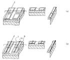
本発明では、共振器面をエッチングにより形成しているが、その時のエッチングでは、n型半導体層の一部が露出するまでの深さとすることが好ましく、特にn型コンタクト層が露出するまでの深さまでしかエッチングしないのが好ましい。これにより、ウインドウ領域の形成領域を端面全面ではなく、導波路領域近傍の限られた領域とすることができる。また、エッチングを基板が露出するまで行わず、比較的浅い位置までとすることで、エッチングによる共振器面の荒れを少なくすることができる。しかし、そうなると、チップ化の際に、分割位置に厚い半導体層が残っていることになるので、所望の位置で分割しにくくなることがある。このような問題を解決するために、対向する共振器面の間を更にエッチングして、図4(e)に示すように、共振器面より突出するn型半導体層突出部を設けることができる。このように、n型半導体層突出部を設けることで、ウインドウ領域の形成領域を小さくして光損失を低減するとともに、素子分割時を容易にすることができる。尚、このn型半導体層突出部は、図4(a)〜(d)に示すような第1の保護膜、第2の保護膜及び電極等を形成した後に行うのが好ましい。
【0071】
n型半導体層突出部を設けることで、ウインドウ領域の形成領域を小さくして、素子特性を改良することができ、また、製造工程上においても有利である。すなわち、チップ化し易くするためには、ある程度の深さまでエッチングすることが必要であるが、それを一度のエッチングではなく、2段階のエッチングを行うことで、共振器面が荒れることを抑制し、鏡面に近い面として形成させることができる。エッチングは化学的に半導体層を削りながら除去するものであるが、その除去する早さは、エッチングガスの種類や条件、或いはマスクの選択比等によって異なる。共振器面は、鏡面に近いような均一な平坦面とするのが好ましいので、エッチング面ができるだけ荒れないように行う。そのためには、エッチング速度がやや遅いエッチングガスを選択するのが好ましい。しかし、そのような速度で成長基板までエッチングすると、時間がかかり過ぎるためにマスクが保たなくなり、共振器面が荒れてしまう。そのため、共振器面を形成するために少なくともn型半導体層の一部が露出するまでゆっくりエッチングした後、別のマスクを形成して共振器面を保護して異なる条件でエッチングを行う。この場合、エッチングされるのはn型半導体層のみであるので、共振器面のような鏡面でなくともよく、粗面になってもビーム特性に与える影響は比較的少ない。そのため、速度の速いエッチングガスを選択することができる。このように2段階のエッチングを行うことで、優れた共振器面を得ることができる。このような工程を設けることで、対向する共振器面間の半導体層の膜厚を薄くして、分割時に破損しにくくなるようにすることができる。
【0072】
共振器面形成後、その間のエッチングする時には、共振器面を何らかの保護膜で被覆するのが好ましい。保護膜としては、後で除去してしまうエッチングマスクでもよいし、又、後でミラー等として残存される保護膜でもよい。また、この場合の保護膜の膜厚(共振器面上での膜厚)としては、薄くするのが好ましい。これは、共振器面からn型半導体層の突出部の端面までの長さが変わってくるためであり、共振器面から出射されるレーザ光を遮らないようにするには、n型半導体層の突出部は少ない方が好ましい。但し、エッチング時に保護膜下の半導体層が変質しない程度の膜厚は必要である。これにより、ファーフィールドパターン(FFP)のy成分にリップル(凹凸)が生じない、優れたビーム特性を有する半導体レーザ素子とすることができる。また、n型半導体層の突出部形成時のエッチングは、基板が露出するまで行ってもよい。そうすると、チップ化する際に、基板のみを分割すればよいことになる。
【0073】
また、このn型突出部形成工程は、ウインドウ領域形成後に行うのが好ましい。ウインドウ領域よりも先にn型半導体層の突出部を形成させると、その突出部の端面にまでウインドウ領域である半導体層が形成されるので、好ましくない。ウインドウ領域は、活性層よりもバンドギャップの大きい半導体層からなるが、そのような層が、n型半導体層の突出部にまで形成されていると、活性層を含む導波路領域から洩れだした光(迷光)が、導波路領域より下(基板側)の端面であるn型半導体層の突出部から外部に放出されることになるので、それにより主ビームにノイズが生じるなどの問題が生じるので好ましくない。また、後の分割性を考慮して対向する共振器面の間の半導体層を薄くするために、n型半導体層の突出部を形成させるが、その対向する突出部の間にウインドウ領域形成によって半導体層が積層されてしまうと分割性が悪くなる。チップサイズを大きくすれば、対向するn型半導体層の突出部の間の距離を大きくして、半導体層が成長しにくい保護膜等を設けることも可能であるが、歩留まりが低下するので好ましくない。
【0074】
【実施例】
本発明において、窒化物半導体層を構成するp型半導体層、活性層、n型半導体層のデバイス構造としては、特に限定されず、種々の層構造を用いることができる。デバイスの具体的な構造としては、例えば後述の実施例に記載されているデバイス構造が挙げられる。また、電極、絶縁膜(保護膜)等も特に限定されず種々のものを用いることができる。窒化物半導体の具体的な例としては、GaN、AlN、若しくはInNなどの窒化物半導体や、これらの混晶であるIII−V族窒化物半導体(InxAlyGa1−x−yN、0≦x、0≦y、x+y≦1)を用いることができる。窒化物半導体の成長は、MOVPE、MOCVD(有機金属化学気相成長法)、HVPE(ハライド気相成長法)、MBE(分子線気相成長法)等、窒化物半導体を成長させるのに知られている全ての方法を適用できる。
以下、実施例として窒化物半導体を用いた半導体レーザ素子について説明するが、本発明の半導体レーザ素子は、これに限らず、本発明の技術的思想において、様々な半導体に実施できることは言うまでもない。
【0075】
[実施例1]
(バッファ層) 実施例1では、基板としてサファイアを用いる。2インチφ、C面を主面とするサファイアよりなる異種基板をMOVPE反応容器内にセットし温度を500℃にしてトリメチルガリウム(TMG)、アンモニア(NH3)を用い、GaNよりなるバッファ層を200Åの膜厚で成長させる。
【0076】
(下地層) バッファ層形成後、温度を1050℃にして、TMG、アンモニアを用い、アンドープGaNよりなる窒化物半導体層を4μmの膜厚で成長させる。この層は、素子構造を形成する各層の成長において下地層(成長基板)として作用する。下地層としてこの他にELO(Epitaxially Laterally Overgrowth)成長させた窒化物半導体を用いると結晶性が良好な成長基板が得られる。ELO成長層の具体例としては、異種基板上に、窒化物半導体層を成長させ、その表面に窒化物半導体の成長が困難な保護膜を設ける等して形成したマスク領域と、窒化物半導体を成長させる非マスク領域とをストライプ状に設け、その非マスク領域から窒化物半導体を成長させることで、膜厚方向への成長に加えて横方向への成長が成されることにより、マスク領域にも窒化物半導体が成長して成膜させたものや、異種基板上に成長させた窒化物半導体層に開口部を設け、その開口部側面から横方向への成長が成されて成膜されたもの等が挙げられる。
次に、窒化物半導体からなる下地層の上に、積層構造体を構成する各層を形成する。
【0077】
(n型コンタクト層)
続いて1050℃で、同じく原料ガスにTMG、アンモニアガス、不純物ガスにシランガスを用い、Siを4.5×10¹⁸/cm3ドープしたGaNよりなるn型コンタクト層を2.25μmの膜厚で成長させる。このn型コンタクト層の膜厚は2〜30μmであればよい。
【0078】
(クラック防止層)
次に、TMG、TMI(トリメチルインジウム)、アンモニアを用い、温度を800℃にしてIn0.06Ga0.94Nよりなるクラック防止層を0.15μmの膜厚で成長させる。なお、このクラック防止層は省略可能である。
【0079】
(n型クラッド層)
次に、温度を1050℃にして、原料ガスにTMA(トリメチルアルミニウム)、TMG及びアンモニアを用い、アンドープのAlGaNよりなるA層を25Åの膜厚で成長させ、続いてTMAを止め、不純物ガスとしてシランガスを用い、Siを5×10¹⁸/cm3ドープしたGaNよりなるB層を25Åの膜厚で成長させる。そしてこの操作をそれぞれ160回繰り返してA層とB層を交互に積層し、総膜厚8000Åの多層膜(超格子構造)よりなるn型クラッド層を成長させる。この時、アンドープAiGaNのAlの混晶比としては、0.05以上0.3以下の範囲であれば、十分にクラッド層として機能する屈折率差を設けることができる。
【0080】
(n型光ガイド層)
次に、同様の温度で原料ガスにTMG及びアンモニアを用い、アンドープのGaNよりなるn型光ガイド層を0.1μmの膜厚で成長させる。この層は、n型不純物をドープさせてもよい。
【0081】
(活性層)
次に、温度を800℃にして、原料にTMI(トリメチルインジウム)、TMG及びアンモニアを用い、不純物ガスとしてシランガスを用い、Siを5×10¹⁸/cm3ドープしたIn0.05Ga0.95Nよりなる障壁層を100Åの膜厚で成長させる。続いてシランガスを止め、アンドープのIn0.1Ga0.9Nよりなる井戸層を50Åの膜厚で成長させる。この操作を3回繰り返し、最後に障壁層を積層させて総膜厚550Åの多重量子井戸構造(MQW)の活性層を成長させる。レーザ光の発振波長を変更させる場合は、活性層の組成を変更することで所望の波長とすることができる。特にInの混晶比を選択することで近紫外域から可視光までの波長領域とすることができる。
【0082】
(p型キャップ層)
次に、同様の温度で、原料ガスにTMA、TMG及びアンモニアを用い、不純物ガスとしてCp2Mg(シクロペンタジエニルマグネシウム)を用い、Mgを1×10¹⁹/cm3ドープしたAlGaNよりなるp型電子閉じ込め層を100Åの膜厚で成長させる。
【0083】
(p型光ガイド層)
次に、温度を1050℃にして、原料ガスにTMG及びアンモニアを用い、アンドープのGaNよりなるp型光ガイド層を750Åの膜厚で成長させる。このp型光ガイド層はアンドープとして成長させるが、Mgをドープさせてもよい。
【0084】
(p型クラッド層)
続いて、1050℃でアンドープAl0.16Ga0.84Nよりなる層を25Åの膜厚で成長させ、続いてTMGを止め、Cp2Mgを用いてMgドープGaNよりなる層を25Åの膜厚で成長させ、総膜厚0.6μmの超格子層よりなるp型クラッド層を成長させる。p型クラッド層は少なくとも一方がAlを含む窒化物半導体層を含み、互いにバンドギャップエネルギーが異なる窒化物半導体層を積層した超格子で作製した場合、不純物はいずれも一方の層に多くドープして、いわゆる変調ドープを行うと結晶性がよくなる傾向にあるが、両方に同じようにドープさせてもよい。
【0085】
(p型コンタクト層)
最後に1050℃でp型クラッド層の上にMgを1×10²⁰/cm3ドープしたp型GaNよりなるp型コンタクト層を150Åの膜厚で成長させる。p型コンタクト層はp型のInxAlyGa1−x−yN(x≦0、y≦0、x+y≦1)で構成することができ、好ましくはMgをドープしたGaNとすればp電極と最も好ましいオーミック接触が得られる。反応終了後、反応容器内において窒素雰囲気中でウエハを700℃でアニーリングして、p型層を更に低抵抗化する。
【0086】
(表面保護膜形成)
以上のようにして窒化物半導体層を積層した後、ウエハを反応容器から取り出し、最上層のp型コンタクト層の表面にAlNからなる表面保護膜をMOCVD装置を用いて形成する。このとき、AlNの膜厚は約200Åである。
【0087】
(エッチングマスク形成)
表面保護膜の上に、共振器面がサファイア基板のオリフラ面(A面)に略平行となるようにエッチングマスクを形成させる。エッチングマスクとしては、SiO2を用い、CVD装置を用いて膜厚約3μmとなるよう形成させる。
【0088】
(n型層露出及び共振器面形成)
以上のようにしてエッチングマスクを形成した後、RIE(反応性イオンエッチング)を用いSiCl4ガスによりエッチングし、n電極を形成させるためのn型コンタクト層の表面を露出させる。この時、共振器面となる活性層端面を露出させてエッチング端面を共振器面とする。
【0089】
(ウインドウ領域形成)
次に、上記のようにして得られる表面保護膜とエッチングマスクとが形成されている状態のウエハをMOCVD装置内に設置し、温度を1050℃にして、原料ガスとしてTMA(トリメチルアルミニウム)、TMG及びアンモニアを用い、アンドープのAlGaNよりなるウインドウ領域を膜厚(共振器面からの膜厚)を5000Åで成長させる。尚、このとき、n型コンタクト層及び、ウインドウ領域形成端面以外の端面等についても、AlN等の表面保護膜を形成させる。
【0090】
次いで、表面保護膜及びエッチングマスクを除去する。まず、フッ酸でエッチングマスクのSiO2を溶解除去し、その後に現像液を用いて表面保護膜であるAlNをエッチングにより除去する。これにより、共振器面及び対向する共振器面間のn型コンタクト層の露出面にAlGaN層が形成され、p型コンタクト層の表面が露出されたウエハが得られる。共振器面に形成されているAlGaN層は、ウインドウ領域として機能する層である。
【0091】
(ストライプ状リッジ形成)
次に、ストライプ状の導波路領域を形成するために、最上層のp型コンタクト層のほぼ全面にCVD装置により、Si酸化物(主としてSiO2)よりなる保護膜を0.5μmの膜厚で形成した後、保護膜の上に所定の形状のマスクをかけ、RIE装置によりCF4ガスを用いたフォトリソグラフィー技術によりストライプ状の保護膜を形成して、活性層よりも上にストライプ状のリッジが形成される。
【0092】
(第1の絶縁膜)
SiO2マスクをつけたまま、p型半導体層表面にZrO2よりなる第1の絶縁膜を形成する。この第1の絶縁膜は、n側オーミック電極形成面をマスクして半導体層の全面に設けてもよい。また、後に分割され易いように絶縁膜を形成させない部分を設ける。第1の絶縁膜形成後、バッファード液に浸漬して、ストライプ状リッジの上面に形成したSiO2を溶解除去し、リフトオフ法によりSiO2と共に、p型コンタクト層上(更にはn型コンタクト層上)にあるZrO2を除去する。これにより、リッジの上面は露出され、リッジの側面はZrO2で覆われた構造となる。
【0093】
(オーミック電極)
次に、p型コンタクト層上のリッジ最表面及び第1の絶縁膜上にp側オーミック電極を形成させる。このp側オーミック電極は、Ni−Auからなる。また、n型コンタクト層上面にもn側オーミック電極を形成させる。n側オーミック電極はTi−Alからなり、リッジと平行で、かつ、同程度の長さのストライプ状に形成されている。これら電極形成後、酸素:窒素が80:20の割合の雰囲気中で、600℃でアニーリングすることで、p側及びn側オーミック電極を合金化し、良好なオーミック特性を有するオーミック電極とする。
【0094】
(第2の絶縁膜)
次いで、SiO2及びZrO2からなる誘電体多層膜を、ウインドウ領域を形成させている出射側共振器面を除いてほぼ全面に形成させる。SiO2とZrO2は交互に3ペア積層させることで、モニター側の共振器面のミラーとして機能する。その後、リッジ上部のp側オーミック電極とn側オーミック電極の一部にレジストを塗布し、ドライエッチングすることでそれぞれの電極の一部を露出させる。
【0095】
(パッド電極)
次に、上記の第2の絶縁膜を覆うようにp側パッド電極及びn側パッド電極を形成する。このパッド電極は、Ni−Ti−Auからなり、第2の絶縁膜を介してp側オーミック電極及びn側オーミック電極にそれぞれストライプ状に接している。
【0096】
(n型半導体層の突出部形成)
次に、先の共振器面形成時のエッチングによって露出されているn型コンタクト層を更にエッチングしてn型半導体層の突出部を形成させる。まず、SiO2をウエハ前面に形成した後、その上にn型コンタクト層の露出面を除いてレジスト膜を形成し、基板が露出するまでエッチングする。これにより、先に形成させたウインドウ領域と、そのウインドウ領域から突出するn型半導体層の突出部が形成される。また、このn型半導体層の突出部は、ウインドウ領域を形成していない側の共振器面(モニター側共振器面)側にも形成することができる。
【0097】
(出射面側保護膜形成)
上記のように形成されたウインドウ領域に出射面側保護膜としてSiO2とZrO2よりなる誘電体保護膜を形成する。この出射面側保護膜は、モニター側保護膜よりも低反射率となるように設計する。
次いで、リッジストライプに垂直な方向で基板側からバー状に割り、最後にリッジストライプと平行な方向でバーを切断して本発明の窒化物半導体レーザ素子を得る。
【0098】
以上のようにして得られる窒化物半導体レーザ素子は、室温において閾値2.0kA/cm2、30mWの高出力において、発振波長405nmの連続発振が確認され、また、CODを発生せず、良好なビームが得られる。
【0099】
[実施例2]
実施例2では、表面保護膜をPtとし、これをエッチングマスクを兼用する表面保護膜として用いる以外は実施例1と同様に行い、本発明の窒化物半導体レーザ素子を得る。この場合、ウインドウ領域形成後に、Ptを除去する際に王水を用いる。以上のようにして得られる窒化物半導体レーザ素子は、室温において閾値2.0kA/cm2、30mWの高出力において、発振波長405nmの連続発振が確認され、また、CODを発生せず、良好なビームが得られる。
【0100】
[実施例3]
実施例3では、p型半導体層の表面にSiO2からなるエッチングマスクを形成して共振器面を形成し、ウインドウ領域形成前にSiO2を除去し、その除去により露出されるp型半導体層表面及びウインドウ領域を形成させる端面以外に表面保護膜としてAlNを設ける以外は、実施例1と同様に行う。以上のようにして得られる窒化物半導体レーザ素子は、室温において閾値2.0kA/cm2、30mWの高出力において、発振波長405nmの連続発振が確認され、また、CODを発生せず、良好なビームが得られる。
【0101】
[実施例4]
実施例4では、実施例1の出射側保護膜を形成後に、リッジから離間する位置にSiO2(1350Å)/Ti(2500Å)からなる遮光膜を形成する以外は、実施例1と同様に行い本発明の窒化物半導体レーザ素子を得る。以上のようにして得られる窒化物半導体レーザ素子は、室温において閾値2.0kA/cm2、30mWの高出力において、発振波長405nmの連続発振が確認され、また、CODを発生せず、FFP−xにおいてもリップルのない良好なビームが得られる。
【0102】
[実施例5]
実施例5では、リッジを3本有するマルチストライプ型の窒化物半導体レーザ素子を形成させる以外は実施例1と同様に行い、本発明の窒化物半導体レーザ素子を得る。得られる窒化物半導体レーザ素子は、室温において閾値2.0kA/cm2、100mWの高出力において発振波長405nmの連続発振が確認され、また、CODも発生せず、良好なビームが得られる。
【0103】
[実施例6]
実施例6では、ウインドウ領域形成後、リッジストライプ形成後に、成長基板を除去し、露出したn型半導体層にCu−Wからなる支持基板を接合する以外は実施例6と同様に行い、本発明の窒化物半導体レーザ素子を得る。得られる窒化物半導体レーザ素子は、室温において閾値2.0kA/cm2、30mWの高出力において発振波長405nmの連続発振が確認され、また、CODも発生せず、良好なビームが得られる。
【発明の効果】
本発明の窒化物半導体レーザ素子は、n型半導体層の突出部を有し、その突出部の端面にはウインドウ領域を設けないようにすることで、共振器面に設けられるウインドウ領域の形成面積を小さくすることができる。これにより、ウインドウ領域を伝搬して出射部以外の端面から光が放出されるのを抑制することができるので、ビーム特性の良好な窒化物半導体レーザ素子とすることができる。また、本発明の半導体レーザ素子の製造方法は、ウインドウ領域を有する窒化物半導体レーザ素子のように、窒化物半導体層を成長後に、層を加工する工程を経て、その後に窒化物半導体からなる成長層を成長させるという再成長工程を含む窒化物半導体レーザ素子に適用することができる。特に、p型半導体層まで成長させた後に再成長工程を有する場合に、SiO2などp型コンタクト層に拡散しやすい材料からなるエッチングマスクを半導体層に直接接しないようにすることで、再成長時にエッチングマスクの構成元素が半導体層内に拡散するのを抑制することができるので、結晶性の悪化を抑制し、かつ、電気的特性を劣化しにくくすることができる。これにより、寿命特性に優れた半導体レーザ素子とすることができ、しかも、ウインドウ領域を有することで、端面劣化を生じにくい半導体レーザ素子を得ることができる。
【図面の簡単な説明】
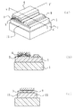
【図1】(a)本発明の実施の形態の窒化物半導体レーザ素子を説明する斜視図、(b)図1(a)のX−X‘断面図、(c)図1(a)のY−Y’断面図
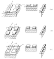
【図2】(a)〜(c)本発明の工程を説明する斜視図及び断面図
【図3】(a)〜(b)本発明の工程を説明する斜視図及び断面図
【図4】(a)〜(e)本発明の工程を説明する斜視図及び断面図
【符号の簡単な説明】
1・・・基板
2・・・n型窒化物半導体層
3・・・p型窒化物半導体層
4・・・活性層
5・・・p側オーミック電極
6・・・p側パッド電極
7・・・n側オーミック電極
8・・・n側パッド電極
9・・・ウインドウ領域
10・・・リッジストライプ
11・・・第1の絶縁膜
12・・・第2の絶縁膜
13・・・第1の保護膜(表面保護膜)
14・・・エッチングマスク
15・・・n型半導体層突出部[0001]
BACKGROUND OF THE INVENTION
The present invention relates to a nitride semiconductor laser device having a stripe-shaped waveguide region, and more particularly to a nitride semiconductor laser device having a window structure on an end face and capable of high output, and in particular, a nitride semiconductor on a resonator surface. The present invention relates to an edge growth type window structure obtained by regrowth. As a specific composition used in the nitride semiconductor laser device of the present invention, a GaN, AlN, InN, or a III-V group nitride semiconductor (InxAlyGa1-xyN, 0 ≦ x, 0 ≦ y, x + y ≦ 1).
[0002]
[Prior art]
In recent years, semiconductor lasers have become small, long-life, highly reliable, and have high output, and are mainly used for electronic devices such as personal computers and DVDs, medical equipment, processing equipment, and light sources for optical fiber communication. . Above all, nitride semiconductors (InxAlyGa1-xyN, 0.ltoreq.x, 0.ltoreq.y, and x + y.ltoreq.1) are attracting attention as semiconductor lasers capable of emitting red light from a relatively short wavelength ultraviolet region.
[0003]
A nitride semiconductor laser device includes a buffer layer, an n-type contact layer, a crack prevention layer, an n-type cladding layer, an n-type light guide layer, an active layer, a p-type light guide layer, a p-type cap layer, and a p-type on a sapphire substrate. A clad layer, a p-type contact layer, and the like are sequentially laminated. A ridge stripe is formed on such a laminated structure to provide a striped waveguide region, and a resonator surface is formed on the end surface of the waveguide region.
[0004]
In such a nitride semiconductor laser element, since it is not always easy to form the resonator surface by cleavage, it has been studied to form the resonator surface by etching. As an etching method, dry etching such as reactive ion etching (RIE) capable of anisotropic etching is preferably used. Since the etched surface formed by such RIE has more irregularities than the cleaved surface, the reflection loss increases. As a technique for solving such a problem, a loss can be compensated by providing a dielectric protective film or the like on the resonator surface. However, even if such a dielectric protective film is provided, it cannot sufficiently withstand high output. In order to solve such a problem, there is a technique of providing a protective film (window region) having a wider band gap than the active layer. By providing the window region, it is possible to suppress deterioration of the end face.
[0005]
[Patent Document 1]
Japanese Patent Application Laid-Open No. 07-249830
[0006]
[Problems to be solved by the invention]
However, if the window region is formed not only in the vicinity of the waveguide region but also in a wide end surface region, the light from the active layer propagates through the window region, which may cause a problem of increased light loss. is there. Further, in the manufacturing method of the window region, since the resonator surface by etching is in a direction substantially perpendicular to the growth surface of the semiconductor layer, there is a problem that it is difficult to obtain a window region having a uniform film quality when grown as a wafer. is there. Further, when the window region is grown, there is a problem that the device characteristics are deteriorated depending on the growth temperature. In view of the above problems, an object of the present invention is to provide a nitride semiconductor laser element with little optical loss due to a window region. It is another object of the present invention to provide a method for manufacturing a nitride semiconductor laser device, in which a window region having a uniform film quality is obtained, and deterioration of device characteristics when the window region is formed is suppressed.
[0007]
[Means for Solving the Problems]
The nitride semiconductor laser element in the present invention isFormed on the substrateA nitride semiconductor having a waveguide region made of a ridge stripe in a nitride semiconductor layer made of an n-type semiconductor layer, an active layer, and a p-type semiconductor layer, and having a wider band gap than the active layer on the resonator surface of the waveguide region A nitride semiconductor laser device having a window region, wherein the nitride semiconductor layer has an n-type semiconductor layer protruding portion that partially protrudes from the resonator surface, and the window region is formed of a p-type semiconductor layer. It is formed in the end face region from the end face to the end face of the n-type semiconductor layer on the active layer side from the n-type semiconductor layer protrusion.The surface of the substrate is exposed from the n-type semiconductor layer protrusion.It is characterized by that.
[0008]
In the nitride semiconductor laser element according to
[0009]
The nitride semiconductor laser device according to claim 3 of the present invention is characterized in that the window region is covered with a light shielding film in a region separated from the waveguide region.
[0010]
The nitride semiconductor laser device according to
[0011]
In the nitride semiconductor laser device according to claim 5 of the present invention, the active layer is made of In.xGa1-xN (0 ≦ x ≦ 1), and the window region is made of Al.yGa1-yN (0 ≦ y ≦ 1).
[0013]
Of the present inventionClaim 6The nitride semiconductor laser device manufacturing method described inOn the boardAfter laminating a nitride semiconductor layer composed of an n-type semiconductor layer, an active layer, and a p-type semiconductor layer, a resonator surface is formed by etching, and the resonator surface is made of a nitride semiconductor having a wider band gap than the active layer. A method of manufacturing a nitride semiconductor laser device for forming a window region,After the window region is formed, the semiconductor layer between the opposing resonator surfaces is further etched to form an n-type semiconductor layer protruding portion protruding from the resonator surface, from the n-type semiconductor layer protruding portion The element division is performed in the exposed region.
In the method for manufacturing a nitride semiconductor laser device according to claim 7 of the present invention, the window region is formed with a surface protective film formed on an upper surface of the p-type semiconductor layer and the surface protective film being provided. It is characterized by.
[0014]
The method for manufacturing a nitride semiconductor laser device according to claim 8 of the present invention is characterized in that a ridge stripe is formed after the window region is formed.
[0016]
Of the present inventionClaim 9The nitride semiconductor laser device described in 1 is characterized in that the resonator surface is an M-plane of a nitride semiconductor.
[0017]
Of the present inventionClaim 10The method for manufacturing a nitride semiconductor laser device described in 1) is characterized in that the surface protective film is an etching mask for forming the resonator surface.
[0018]
Of the present inventionClaim 11The method for manufacturing a nitride semiconductor laser device described in 1) is characterized in that the surface protective film includes a first protective film between the etching mask and the nitride semiconductor layer.
[0019]
Of the present inventionClaim 12The method for manufacturing a nitride semiconductor laser device according to 1 is characterized in that the first protective film is formed to be equal to or larger than the etching mask.
[0020]
Of the present inventionClaim 13The method for manufacturing a nitride semiconductor laser element described in 1) is characterized in that the first protective film is a nitride semiconductor.
[0021]
Of the present inventionClaim 14The method for manufacturing a nitride semiconductor laser device described in 1) is characterized in that the first protective film is AlN.
[0022]
Of the present inventionClaim 15The method of manufacturing a nitride semiconductor laser device according to
The method of manufacturing a nitride semiconductor laser device according to claim 16 of the present invention is characterized in that the step of forming the n-type semiconductor layer protruding portion performs etching until the substrate is exposed.
[0023]
DETAILED DESCRIPTION OF THE INVENTION
The nitride semiconductor laser device according to the embodiment of the present invention includes a nitride semiconductor layer including an n-type semiconductor layer, an active layer, and a p-type semiconductor layer. A ridge stripe is formed in the p-type semiconductor layer, whereby a stripe-shaped effective refractive index type waveguide region is provided. A resonator region provided so as to be orthogonal to the stripe-shaped waveguide region has a window region made of a semiconductor layer having a wider band gap than the active layer.
[0024]
The nitride semiconductor laser device of the present embodiment has an n-type semiconductor
[0025]
(Window area)
When a resonator surface is formed on a nitride semiconductor layer grown to a p-type semiconductor layer, a surface state exists on the resonator surface. When the element is driven, the surface level promotes non-radiative recombination to generate heat, and the generation of this heat causes a phenomenon that the band gap on the resonator surface is reduced. Since the light is easily absorbed when the band gap becomes small, this causes a cycle in which the temperature rise of the resonator surface is further accelerated and the band gap becomes small. Due to such a phenomenon, the resonator surface is finally melted to generate COD. The window region is for suppressing such a phenomenon, and by providing a nitride semiconductor having a wider band gap than the active layer on the resonator surface, it is possible to suppress light absorption due to the reduction of the band gap. it can.
[0026]
In the nitride semiconductor laser device of the present embodiment, the window region as described above is formed not in the entire end face but in the vicinity of the waveguide region including the active layer. Specifically, the etching for forming the resonator surface is performed up to a depth at which a part of the n-type semiconductor layer is exposed, the same plane region as the resonator surface is reduced, and a window region is formed in that region. As described above, since the window region is a nitride semiconductor layer having a wider band gap than the active layer, it is a layer that absorbs light but is capable of propagating light. Therefore, light can propagate while reflecting in the window region due to the difference in refractive index from the outside and the difference in refractive index from the interface with the nitride semiconductor layer, so that the light is emitted from the waveguide region including the active layer. The transmitted light is propagated throughout the window area. In the nitride semiconductor laser device of the present embodiment, the area where light is propagated can be reduced by reducing the formation area of such a window region. Thereby, it is possible to make it difficult for FFP to be disturbed due to light propagating to a position away from the waveguide region and light emitted from other than the exit surface. That is, by reducing the formation area of the window region, a nitride semiconductor laser element with little deterioration of beam characteristics due to the window region can be obtained.
[0027]
The size of the window region can be appropriately selected depending on the position where the n-type semiconductor layer protrusion is formed. It is necessary to form at least the end face of the active layer, and when it has a light guide layer, it is necessary to form it on the end face of the waveguide region including that layer. The layer outside the guide layer, for example, the end surface of the cladding layer, may not be provided in the sense of suppressing light absorption. However, if it is not provided, the difference in refractive index near the resonator surface increases, and the beam Since it may adversely affect the characteristics, it is preferably provided. As for the contact layer, the n-type contact layer is not necessary to be provided because the distance from the waveguide region is large, but the p-type contact layer is closer to the active layer than the n-type contact layer, and its film thickness is also thin. It is preferable to provide it.
[0028]
The thickness of the window region is preferably in the range of 100 to 10 [mu] m, more preferably 1000 to 1 [mu] m, and still more preferably 400 to 7000 [mu] m. If the thickness of the window region is smaller than 100 mm, it is difficult to function as the window region, which is not preferable. Moreover, since it will deteriorate an optical characteristic when it becomes larger than 10 micrometers, it is unpreferable. Further, it is preferable not to protrude from the end of the n-type semiconductor layer protrusion, and more preferably not to be provided above the n-type semiconductor layer protrusion that is separated from the resonator surface. .
[0029]
In the present embodiment, the active layer of the nitride semiconductor laser element is InxGa1-xWhen it is a layer containing N (0 ≦ x ≦ 1), the window region is made of Al.yGa1-yN (0 ≦ y ≦ 1) is preferable. By including In in the active layer, a nitride semiconductor laser element capable of emitting light in a wide wavelength range from the visible to the ultraviolet region can be obtained. In order to make the band gap wider than that of such an active layer, it is preferable to form a window region having the above composition. By making x and y other than 0 in the above composition formula, it is possible to have different compositions, and it is preferable to change the band gap by a combination of such compositions. In the above composition, when x and y are both 0, the active layer and the window region have the same composition. Even if the composition is the same, the band gap is changed depending on the growth conditions, film thickness, and the like. Therefore, when it is difficult to change the composition, the same composition can be obtained.
[0030]
(N-type semiconductor layer protrusion)
The nitride semiconductor laser device of the present embodiment has a shape such that the end face of the n-type semiconductor layer partially projects in order to provide the window region in a limited region near the waveguide region. By adopting such an end face shape, it becomes easy to reduce the formation area of the window area without using a mask material or the like. In particular, it is difficult to provide a mask for regrowth on a part of the end surface including the resonator surface as it is on the wafer, and even if it can be formed, it is difficult to form it with good control and the film quality of the mask is sufficient. Is difficult to obtain. For this reason, the film quality of the window region tends to be insufficient. By adopting the end face shape as in the present embodiment, a window region made of a semiconductor with uniform film quality can be obtained.
[0031]
The n-type semiconductor layer included in the protruding portion of the n-type semiconductor layer can be controlled by the etching depth when forming the resonator surface. For example, if the n-type contact layer is etched halfway during the formation of the resonator surface, the n-type semiconductor layer protruding portion can be a part of the n-type contact layer, a base layer, a buffer layer, or the like. Further, when the substrate is provided on the n-type semiconductor layer side, the substrate may be regarded as a part of the n-type semiconductor layer protruding portion.
[0032]
Further, as described above, it is preferable that the distance from the end face of the n-type semiconductor layer protruding portion to the resonator surface is larger than the film thickness of the window region on the resonator surface. As a result, the n-type semiconductor layer protruding portion protrudes from the window region, so that the window region can be used without being cleaved or etched by a subsequent process. In other words, the window region formed by regrowth of the semiconductor on the resonator surface can be used as the exit surface as it is, so that the light loss can be extremely reduced. However, if the n-type semiconductor layer protruding portion protrudes too much from the window region, the light emitted from the waveguide region is blocked by the n-type semiconductor layer protruding portion, and the beam shape deteriorates. It is necessary to make it unobstructed.
[0033]
(Light shielding film)
As described above, the window region is a layer that hardly absorbs light, and the light from the active layer is a layer that propagates in the same manner as inside the device. Therefore, the light emitted from the resonator surface propagates in the window region and is emitted to the outside from an arbitrary position. When such light is mixed with the main beam of laser light, irregularities (ripples) occur in the light distribution, and FFP deteriorates. In order to improve such a phenomenon, a portion of the surface of the window region that is separated from the waveguide region can be covered with a light shielding film. As described above, by providing the light shielding film on the end face including the end face of the active layer separated from the ridge stripe, the ripple generated in the x component of the FFP can be reduced. The light shielding film may be any film that can shield light from the active layer. For example, Ni, Cr, Ti, Cu, Fe, Zr, Hf, Nb, W, Rh, Ru, Mg, Ga A material using Pt, Au, Si, Pd, V, Ta, Mo, C, or the like can be selected. More preferably, it is a material using Ni, Cr, Ti, or Si. These oxides can also be used. The above materials can be used as a single layer film or a multilayer film.
[0034]
Next, each layer and configuration of the nitride semiconductor laser device of the present invention will be described in detail.
(Nitride semiconductor)
As the semiconductor layer used as the nitride semiconductor laser element of the present invention, GaN, AlN, InN, and a III-V group nitride semiconductor (InxAlyGa1-xyN, 0 ≦ x, 0 ≦ y, x + y ≦ 1) are preferable. The nitride semiconductor laser device of the present invention will be specifically described below.
[0035]
(Growth substrate)
The growth substrate may be a different substrate or the same substrate as long as the nitride semiconductor layer can be epitaxially grown, and the size, thickness, and the like are not particularly limited. As a specific example, in a dissimilar substrate, sapphire or spinel (MgA1) whose main surface is any one of the C-plane, R-plane, and A-plane.2OFourInsulating substrates such as silicon carbide (6H, 4H, 3C), silicon, ZnS, ZnO, Si, GaAs, diamond, and oxides such as lithium niobate and neodymium gallate that are lattice-bonded to nitride semiconductors A substrate is mentioned. Further, a nitride semiconductor substrate which is the same kind of substrate can be used as long as it is thick enough to allow device processing (several tens of μm or more).
[0036]
When a heterogeneous substrate is used as the growth substrate, it is preferable to grow the buffer layer before growing the nitride semiconductor layer. As the buffer layer, the general formula AlaGa1-aNitride semiconductor represented by N (0 ≦ a ≦ 0.8), more preferably AlaGa1-aA nitride semiconductor represented by N (0.05 ≦ a ≦ 0.5) is used. The growth temperature of the buffer layer is preferably low temperature growth. Thereby, dislocations and pits on the nitride semiconductor layer can be reduced. Further, Al is formed on the heterogeneous substrate by an ELO (Epitaxial-Lateral-Overgrowth) method.xGa1-xN (0 ≦ X ≦ 1) layers may be grown. Alternatively, a nitride semiconductor that has been laterally grown on the substrate may be formed into a T shape, and after removing the protective film, a nitride semiconductor may be regrown. Although the dissimilar substrate having such a nitride semiconductor layer has dislocations extending on the T-shaped columns, the dislocations are greatly reduced on the upper portions of the T-shaped blades and on the openings of the adjacent T-shaped blades. Therefore, dislocations are reduced even in the regrown junction, so that this substrate has a wide range of low defect regions on the wafer. Therefore, nitride semiconductor laser elements formed on this substrate can be expected to have good life characteristics. Moreover, since the cavity remains after the regrowth by removing the protective film under the T-shaped wings, there is also a warp suppressing effect.
[0037]
Further, although it cannot be used as a growth substrate for the nitride semiconductor layer as described above, a substrate (support substrate) different from the growth substrate can be provided in order to hold the semiconductor layer when driven as a laser element. For example, when the growth substrate is an insulating substrate, a conductive substrate made of metal or the like can be used as the support substrate. When such a conductive support substrate is used, electrodes can be provided on the upper and lower surfaces of the semiconductor layer, so that the resistance inside the element can be reduced. That is, when the growth substrate characteristics (for example, insulation) are harmful when the element is driven (both electrodes are formed on the same surface), the growth substrate is not held as it is, but is made of another material. By bonding to the support substrate, more excellent characteristics can be obtained. Such a support substrate may be on the p-type semiconductor side or the n-side semiconductor layer side, and the material of the support substrate can be appropriately selected. In addition, steps such as separation of the growth substrate and bonding of the support substrate can be performed before or after the window region is formed.
[0038]
(Active layer)
In the nitride semiconductor laser element of the present invention, it is particularly preferable that the active layer has a nitride semiconductor layer containing In. This makes it possible to obtain laser light having a violet to red wavelength in the ultraviolet and visible range. The active layer may have a quantum well structure, and in that case, either a single quantum well or a multi-quantum well may be used. A quantum well structure is preferable, so that a laser element with excellent luminous efficiency and high output can be obtained. Specifically, AlxInyGa1-xyIt is preferable to use a nitride semiconductor represented by N (0 ≦ x ≦ 1, 0 <y ≦ 1, x + y ≦ 1). In this case, the active layer having the quantum well structure means that the nitride semiconductor shown here is preferably used as the well layer. In the wavelength region from near ultraviolet to visible green (from 380 nm to 550 nm), InyGa1-yN (0 <y <1) is preferably used, and in the longer wavelength region (red) beyond that, In is similarly used.yGa1-yN (0 <y <1) can be used. At this time, a desired wavelength can be obtained mainly by changing the In mixed crystal ratio y. In a short wavelength region of 380 nm or less, since the wavelength corresponding to the forbidden band width of GaN is 365 nm, it is necessary to set the band gap energy to be substantially the same as or larger than that of GaN.xInyGa1-xyN (0 <x ≦ 1, 0 <y ≦ 1, x + y ≦ 1) is used.
[0039]
When the active layer has a quantum well structure, the specific well layer thickness is in the range of 10 to 300 mm, preferably in the range of 20 to 200 mm to reduce Vf and the threshold current density. Can be made. Further, from the viewpoint of crystal growth, when the thickness is 20 mm or more, a layer having a relatively uniform film quality without large unevenness in film thickness can be obtained. It becomes possible. The number of well layers in the active layer is not particularly limited and is 1 or more. At this time, when the number of well layers is 4 or more, if the thickness of each layer constituting the active layer increases, the active layer Since the entire film thickness is increased and Vf is increased, it is preferable to keep the film thickness of the active layer low by setting the film thickness of the well layer to 100 mm or less. The well layer may be doped with p-type or n-type impurities (acceptor or donor), or may be undoped or non-doped.
[0040]
The composition of the barrier layer is not particularly limited, and a nitride semiconductor similar to the well layer can be used. Specifically, a nitride semiconductor containing In such as InGaN having a lower In mixed crystal ratio than the well layer, or A nitride semiconductor containing Al, such as GaN or AlGaN, can be used. As a specific composition, InβGa1-βN (0 ≦ β <1, α> β), GaN, AlγGa1-γN (0 <γ ≦ 1) can be used, preferably InβGa1-δBy using N (0 ≦ β <1, α> β) and GaN, a barrier layer can be formed with good crystallinity. In the multi-quantum well structure, the barrier layer sandwiched between the well layers is not limited to one layer (well layer / barrier layer / well layer), and two or more barrier layers may be used. A plurality of barrier layers having different compositions and impurity amounts may be provided, such as “well layer / barrier layer (1) / barrier layer (2) /... / Well layer”. Here, α is the In composition ratio of the well layer, and it is preferable that the In composition ratio β of the barrier layer is smaller than that of the well layer, with α> β. The barrier layer may be doped with an n-type impurity or non-doped, but is preferably doped with an n-type impurity. At this time, the n-type impurity concentration in the barrier layer is at least 5 × 10¹⁶/ Cm3It is preferable to be doped above, and the upper limit is 1 × 10²⁰/ Cm3It is.
[0041]
(P-type cladding layer)
The nitride semiconductor used for the p-type cladding layer only needs to have a sufficient difference in refractive index to confine light, and a nitride semiconductor layer containing Al is preferably used. Further, this layer may be a single layer or a multilayer film, and may have a superlattice structure in which AlGaN and GaN are alternately stacked. Further, this layer may be doped with impurities or may be undoped. In the case of a multilayer film, it may be doped with at least one layer constituting the layer. In the nitride semiconductor laser element having a long oscillation wavelength of 430 to 550 nm, the p-type cladding layer is preferably GaN doped with a p-type impurity. Further, although the film thickness is not particularly limited, it is preferably formed in the range of 100 to 2 μm, more preferably in the range of 500 to 1 μm, and sufficient light confinement effect is obtained. Further, it is preferable that an electron confinement layer and a light guide layer are provided between the active layer and the p-type cladding layer, and the active layer and the light guide layer are sandwiched.
[0042]
(P-type electron confinement layer)
The p-type electron confinement layer provided between the active layer and the p-type cladding layer, preferably between the active layer and the p-type light guide layer is a layer that also functions as confinement of carriers in the active layer, and has a threshold value By reducing the current, it contributes to easy oscillation. Specifically, AlGaN is used. In particular, by providing a p-type semiconductor layer with a p-type cladding layer and a p-type electron confinement layer, a more effective electron confinement effect can be obtained. When AlGaN is used for the p-type electron confinement layer, the function can be exhibited more reliably by doping with a p-type impurity, but the function as a carrier confinement can be achieved even when non-doped. Have. The lower limit of the film thickness is at least 10 mm and preferably 20 mm. The film thickness is 500 mm or less, and AlxGa1-xAs the composition of N, the effect can be sufficiently expected when x is 0 or more, preferably 0.2 or more. Thus, the p-type electron confinement layer is preferably provided in contact with the active layer, so that carriers can be efficiently injected into the active layer or the well layer.
[0043]
(Guide layer)
In the present invention, a p-type and n-type guide layer sandwiching the active layer is provided on the inner side of the p-type and n-type cladding layers to form an optical waveguide, thereby forming an excellent waveguide in a nitride semiconductor. Can do. At this time, the thickness of the waveguide (the active layer and both guide layers sandwiching it) is specifically 6000 mm or less to suppress a rapid increase in the oscillation threshold current, preferably 4500 mm or less. With a low oscillation threshold current, continuous oscillation with a long life in the fundamental mode is possible. Both guide layers are preferably formed with substantially the same film thickness, and the film thickness of the guide layer is preferably set in the range of 100 mm to 1 μm, more preferably 500 mm to 2000 mm. A good optical waveguide can be provided. Furthermore, the guide layer only needs to have an energy band gap sufficient to form a waveguide as compared with the cladding layer provided on the outer side thereof, and may be either a single film or a multilayer film. . In addition, it is possible to form a good waveguide by setting the optical guide layer to a band gap energy that is substantially the same as that of the active layer, preferably larger than that, and in the case of a quantum well structure, The band gap energy is made larger than that of the layer, and preferably larger than that of the barrier layer. Furthermore, by providing the light guide layer with a band gap energy of about 10 nm or more than the emission wavelength of the active layer, a waveguide excellent in light guiding can be formed.
[0044]
(N-type cladding layer)
Similar to the p-type cladding layer, the n-type cladding layer only needs to have a refractive index difference sufficient to confine light, and a nitride semiconductor layer containing Al is preferably used. Further, this layer may be a single layer or a multilayer film. Specifically, as shown in the embodiment, it may have a superlattice structure in which AlGaN and GaN are alternately stacked. In addition, this n-type cladding layer acts as a carrier confinement layer and an optical confinement layer, and in the case of a multilayer film structure, as described above, when a nitride semiconductor containing Al, preferably AlGaN is grown, good. Further, this layer may be doped with an n-type impurity, may be undoped, or may be doped into at least one layer constituting the multilayer film layer. In a laser element having a long oscillation wavelength of 430 to 550 nm, the cladding layer is preferably GaN doped with an n-type impurity. Further, the film thickness is not particularly limited as in the case of the p-type cladding layer, but it is sufficient to form it in a range of 100 to 2 μm, preferably in the range of 500 to 1 μm. Functions as a confinement layer.
[0045]
(electrode)
In the semiconductor laser device of the present invention, the p-side electrode formed on the striped ridge and the n-side electrode provided on the n-side layer (n-type contact layer) are not particularly limited. A material capable of obtaining good ohmic contact with a physical semiconductor can be preferably used. By forming the ridge stripe corresponding to the waveguide region, carriers can be injected efficiently. Further, a nitride semiconductor can be provided so as to be in contact with an insulating film described later. In addition, an ohmic electrode provided so as to be in contact with the semiconductor and a pad electrode made of a material suitable for bonding may be provided. In this embodiment, after forming the first insulating film, an opening is provided to form an ohmic electrode, a second insulating film having an opening is further formed thereon, and a pad electrode is formed thereon It is a structured. Specific examples of materials for the p-side electrode include Ni, Co, Fe, Ti, Cu, Rh, Au, Ru, W, Zr, Mo, Ta, Pt, Ag, and oxides and nitrides thereof. These single layers, alloys, or multilayer films can be used. Examples of the n-side electrode include Ni, Co, Fe, Ti, Cu, Rh, Au, Ru, W, Zr, Mo, Ta, Pt, and Ag. These single layers, alloys, or multilayer films can be used. Can be used.
[0046]
(First insulating layer)
In the nitride semiconductor laser device of the present invention, a part of the nitride semiconductor layer is removed, and an insulating film is formed as a buried layer on the side surfaces of the ridge stripe and the planes on both sides of the ridge continuous to the ridge (surface on which the ridge is provided). (Hereinafter referred to as a first insulating layer) is preferably formed. The material of the first insulating layer is SiO2A material other than the above, preferably an oxide containing at least one element selected from the group consisting of Ti, V, Zr, Nb, Hf, and Ta, SiN, BN, SiC, and AlN. Among these, Zr, Hf oxide, BN, and SiC are particularly preferable. Some of these materials have a property of being somewhat dissolved in hydrofluoric acid, but if used as an insulating layer of a laser element, SiO2 can be used as a buried layer.2Tend to be much more reliable. In general, oxide thin films formed in the gas phase such as PVD and CVD are not easily converted into oxides in which the element and oxygen are equivalently reacted. Although the above elements selected in the present invention are PVD, oxides by CVD, BN, SiC, and AlN are more excellent in reliability regarding insulation than Si oxides. In addition, it is very convenient as a buried layer of a laser element when an oxide whose refractive index is smaller than that of a nitride semiconductor (for example, other than SiC) is selected.
[0047]
The film thickness of the first insulating layer is specifically in the range of 500 to 1 μm, preferably in the range of 1000 to 5000 μm. The reason is that if the thickness is less than 500 mm, it is difficult to ensure sufficient insulation at the time of forming the electrode, and if it is 1 μm or more, the uniformity of the protective film is lost and a good insulating film is not obtained. . Moreover, by being in the preferable range, a uniform film having a good refractive index difference between the ridge (convex portion) and the ridge is formed.
[0048]
(Second insulating layer)
The second insulating layer is provided so as to cover the entire surface of the p-side ohmic electrode except for the upper portion of the ridge. Moreover, it is preferable to provide the p-type semiconductor layer exposed by etching and the side end faces of the active layer so as to be continuous. Preferred materials include SiO2, Al2O3, ZrO2TiO2And a single layer film or a multilayer film.
[0049]
(Resonator surface protective film)
Although a window region is formed on the resonator surface on the light emitting side, a protective film can be provided on the surface of the window region in order to resonate efficiently. In particular, it is preferable to provide a protective film on the monitor-side resonator surface in order to provide a refractive index difference from the emission-side resonator surface. Specific examples of the conductive material include Nb, Ni, Cr, Ti, Cu, Fe, Zr, Hf, Nb, W, Rh, Ru, Mg, Al, Sc, Y, Mo, Ta, Co, and Pd. , Ag, Au, Pt, Ga, and those selected from any of these oxides, nitrides, fluorides and the like can be used. These may be used alone, or may be used as a compound or a multilayer film in which a plurality of them are combined. As the semiconductor material, AlN, AlGaN, BN, Si, InGaN, GaAs, InP, or the like can be used. As the insulator material, compounds such as oxide, nitride, fluoride, etc. of Si, Mg, Al, Hf, Nb, Zr, Sc, Ta, Ga, Zn, Y, B, Ti, Cr can be used. .
[0050]
The end face protective film is preferably formed so as to be in direct contact with the nitride semiconductor layer. Thereby, it is possible to prevent light from being introduced into the inside of the insulating film or the like other than the nitride semiconductor layer, and stray light can be easily emitted to the outside.
[0051]
In the case where a conductive material such as a metal material is used, an insulating layer can be formed on the surface of the nitride semiconductor layer and formed on the insulating layer. Thereby, even a material having poor adhesion to the material with the nitride semiconductor layer can be dealt with.
[0052]
(Production method)
In the method for manufacturing a nitride semiconductor laser device according to the present invention, after sequentially forming an n-type semiconductor layer, an active layer, and a p-type semiconductor layer, a resonator surface is formed by etching, and a window region is formed on the resonator surface. The present invention relates to a manufacturing method of an edge growth type window structure. As described above, the element characteristics can be improved depending on the formation position of the window region, but it is necessary to prevent the element characteristics from being deteriorated when the window region is formed. A method for manufacturing a nitride semiconductor laser device having an edge growth type window structure according to the present invention will be described below. In particular, the manufacturing method in the case of having an n-type semiconductor layer protrusion is also described in detail. The composition and configuration of each layer of the nitride semiconductor layer are not particularly limited, and various types can be used. In addition, since the characteristics of the electrode, the insulating film, and the like change before the window region is formed, they are preferably formed after the window region is formed.
[0053]
(Surface protective film)
The method for manufacturing a nitride semiconductor laser device in the present embodiment prevents the p-type semiconductor layer from being altered when a window region made of a nitride semiconductor is formed on the surface of the cavity surface formed by etching. A surface protective film is provided.
[0054]
When forming a window region composed of a regrowth layer of a nitride semiconductor in a nitride semiconductor layer grown up to a p-type semiconductor layer, it is necessary to first form a resonator surface. Therefore, the laminated semiconductor layer is once taken out from the semiconductor reaction apparatus (growth apparatus), an etching mask having a desired shape is formed, a resonator surface is formed by etching, and then placed in the reaction apparatus again. A window region is grown on the resonator surface. The formation of such a window region is significantly different from the formation of a dielectric protective film such as a mirror in the formation conditions. Specifically, it is the temperature at the time of formation (growth temperature). The dielectric protective film that can be formed in a vacuum state by sputtering or the like has a low reaction temperature, and the nitride semiconductor element is unlikely to be altered by the temperature. However, the window region can be a semiconductor layer with little light absorption by growing with good crystallinity at the nitride semiconductor growth temperature (about 500 to 1050 ° C.). When growing at a relatively low growth temperature such as the growth temperature of the buffer layer (about 200 to 400 ° C.), the crystallinity of the resulting nitride semiconductor is not good, although the deterioration due to heat can be suppressed. Hard to function as.
[0055]
In the present invention, the region where the window region is not formed is covered with a surface protective film to reduce alteration due to heat at the growth temperature of the semiconductor layer. In particular, the surface of the p-type semiconductor layer close to the active layer is protected by covering it with a surface protective film, thereby suppressing alteration (deterioration) of the active layer. By suppressing the alteration of the p-type contact layer, it is possible to suppress the ohmic contact with the p-side electrode from being inhibited.
[0056]
(Surface protection film and etching mask)
As the surface protective film that covers the surface of the nitride semiconductor layer other than the window region formation region, a stable film that is difficult to be decomposed at the temperature during the growth is used. Such a surface protective film may be used as it is after the etching mask for forming the resonator surface, or may be formed after the etching mask is removed. Alternatively, the etching mask may be left as it is and further formed thereon. In any case, since the etching mask for forming the resonator surface is formed only on the upper surface of the p-type semiconductor layer, it is necessary to separately provide a portion where the window region is not formed in other regions.
[0057]
As materials that can be used as the surface protective film, various materials can be selected as shown in the following (1) to (3).
[0058]
First, (1) a case where an etching mask for forming a resonator surface is used as it is as a surface protective film will be described.
In this case, a material having a selectivity different from that of the nitride semiconductor layer is used as the etching mask. As such a material, any material that does not easily deteriorate by an etching gas may be used. For example, metal or SiO2And the like. As long as it is only etching, there is no particular problem even if any of these is used. However, in the present invention, since a semiconductor growth step (window region forming step) is provided after the etching step, it is necessary to use one that is stable at the semiconductor growth temperature. Accordingly, a metal having a relatively low melting point is not suitable. For example, Ni, Cu, etc. react with the p-type semiconductor layer during the growth of the window region and are not only difficult to remove later, but also deteriorate the crystallinity of the p-type contact layer. Therefore, any material such as Pt that is stable, hardly decomposes, and hardly reacts with the semiconductor layer can be used as it is as a surface protective film when forming the window region.
[0059]
Also, generally used oxides diffuse into the p-type semiconductor layer when the window region is formed, so that the crystallinity is deteriorated and the ohmic contact with the p-side electrode is hindered. In particular, SiO2Although it is excellent as an etching mask, it is not preferable because Si is diffused into the p-type contact layer by decomposition during window region growth. Since Si is also an n-type impurity, if such an element diffuses into the p-type contact layer, the device characteristics are adversely affected. As other materials, an organic compound such as a resist can be used as an etching mask. However, in an apparatus heated to the semiconductor growth temperature, it dissolves or decomposes to contaminate not only the window region but also the inside of the apparatus. This is not preferable.
[0060]
When an etching mask that is unstable against heat as described above is used, it is not used as a single layer, but as shown in FIG. 2A, between the etching
[0061]
Next, (2) a case where a new surface protective film is formed after removing the etching mask at the time of forming the resonator surface will be described.
In such a case, any material that does not easily deteriorate during window region growth can be used. Therefore, the material mentioned as the first protective film in the case (1) can be selected. However, since the etching mask at the time of forming the resonator surface is removed and a surface protective film is formed thereafter, a window region is formed at the edge of the surface of the p-type semiconductor layer. This is because it is technically difficult to form a surface protective film having the same size as the removed etching mask on the surface of the p-type semiconductor layer on which the step is formed by etching. Therefore, depending on the accuracy of the process, the surface protective film may be formed on the resonator surface. Therefore, in order to form the window region at a desired position with good control, the method (1) is preferable. When it is difficult to form the resonator surface by the method (1), for example, diffusion of the etching mask material is prevented. In the case where there is no first protective film suitable for this, it can be formed by the method (2).
[0062]
Moreover, the following method (3) which combined the method of said (1) and (2) can also be used. That is, even when there is no material that can prevent the diffusion of the etching mask as in (2), a new surface protective film is not formed after the resonator surface is formed, but the following method may be used. Good. (3) A first protective film is formed on the surface of the p-type semiconductor layer, an etching mask is formed thereon, a resonator surface is formed by etching, and then only the etching mask is removed, The window region is formed with the protective film remaining. According to this method, the first protective film does not need to prevent the diffusion of the etching mask when forming the window region, and functions as a layer that prevents the window region from being formed at the edge of the surface of the p-type semiconductor layer. Can be made.
As described above, the most preferable method can be selected according to the etching conditions when forming the resonator surface, the conditions when forming the window region, and the formation position.
[0063]
(Cavity plane formation)
After the surface protective film such as the etching mask and the first protective film is formed as described above, etching is performed by using an etching method such as RIE (reactive ion etching) as shown in FIG. Do. As an etching gas, SiCl4, Cl2Etc. can be used. The cavity surface is formed by etching until the end face of the active layer is exposed at least until the end face of the waveguide region including the active layer and the guide layer is exposed. In addition, it is preferable to perform the n-type contact layer so as to be the bottom surface of etching because the n-electrode forming surface can be formed at the same time. Thus, it is preferable to make the etching depth as relatively shallow as it is possible to suppress the roughness of the end face of the active layer. For example, if the substrate is deeply etched until the substrate is exposed, the active layer will be exposed to the etching gas for a long time, making it difficult to maintain the mirror surface. Therefore, by etching up to the end face of the waveguide region and not etching deeper than that, the resonator face can be made difficult to be rough.
[0064]
In the present invention, it is preferable to use a sapphire substrate having a C-plane as a main surface and an A-plane as an orientation flat surface. At this time, by forming the ridge in a direction substantially perpendicular to the orientation flat surface of the sapphire substrate and forming the resonator surface in a direction substantially parallel to the orientation flat surface, the window region can be easily formed with good crystallinity. When the crystal structure of the sapphire substrate and the nitride semiconductor layer is viewed, the resonator surface of the nitride semiconductor layer is formed so as to be substantially parallel to the A surface of the sapphire substrate, thereby nitriding the resonator surface. This is because it can be easily formed as a mirror surface substantially equal to the M-plane of a physical semiconductor. Therefore, the nitride semiconductor grown as the window region can be formed with good crystallinity.
[0065]
(Surface protection film removal)
Of the materials used as the etching mask for forming the resonator surface, it has already been described that there is a material that is preferably formed as it is when the window region is formed. That is, when the first protective film is formed between the etching mask and the p-type semiconductor layer, as shown in FIGS. 2C to 3A, the etching mask and the first protective film are formed after the window region is formed. The surface protective film composed of the
[0066]
(Window area formation)
The wafer having the nitride semiconductor layer after the resonator surface is formed by etching as described above is placed in the MOCVD apparatus, and the temperature in the apparatus is reduced to 500 to 1050 ° C. (10132.5 to 101325 Pa) and normal pressure (101325 Pa) or pressure (101325 to 202650 Pa) are reacted to form a window region as shown in FIG. In FIG. 2C, the window region is formed in a portion other than the surface protective film formed on the surface of the p-type semiconductor layer. It can also be. When the window region is formed at a reaction temperature lower than 500 ° C., the crystallinity of the window region is deteriorated, which is not preferable. When the reaction temperature is higher than 1050 ° C., the active layer of the nitride semiconductor layer is easily decomposed, which is not preferable. . As for the pressure, if it is higher than 202650 Pa, it is not preferable because the window region is difficult to grow, and if it is lower than 10132.5 Pa, the crystallinity of the window region is likely to deteriorate. By setting the reaction conditions of the apparatus in this way and supplying the raw material gas of the semiconductor layer that becomes the window region to perform the reaction, an n-type contact that is an etching bottom surface sandwiched between the resonator surface and the opposing resonator surface A semiconductor layer is grown on the layer.
[0067]
(Ridge stripe formation)
In the nitride semiconductor laser device of the present invention, the ridge is preferably provided on the surface of the p-type semiconductor layer of the nitride semiconductor layer. As a method, SiO is formed on the p-type contact layer of the nitride semiconductor layer.2After an etching mask such as is provided on almost the entire surface, a mask of a predetermined shape is applied on the etching mask, and CHF is applied by an RIE apparatus.3Etching is performed by forming a striped etching mask by a photolithography technique using a gas or the like. As a result, as shown in FIG. 3B, a striped ridge is formed above the active layer. An effective refractive index type waveguide region can be formed by removing a part of the p-type semiconductor layer by etching or the like so that a striped convex portion (ridge) remains. In order to form the ridge, a mask (protective film) is formed in accordance with the desired width of the ridge. Specifically, at a depth that does not reach the light emitting layer composed of at least the active layer and the light guide layer, preferably, the middle of the p-type cladding layer is removed by etching, leaving a striped ridge, Ridge. The structure and characteristics of the laser element vary depending on the etching depth.
[0068]
The number of ridges may be one, or a plurality of ridges may be formed for high output to form a multi-stripe laser element. The width of the ridge is preferably about 1 μm to 3 μm as described above. When providing a plurality of ridges, it is preferable that the widths of the ridges be as equal as possible. If the widths are different, the load applied to each resonator surface will be non-uniform, so it will be easily degraded by the current concentrated in a part.To avoid such a phenomenon, the current is uniformly distributed to each ridge. It is preferable to make it flow.
[0069]
Such a ridge is not limited to a forward mesa shape in which the width of the bottom surface side of the stripe-shaped convex portion is wide and the stripe width decreases as it approaches the upper surface, but conversely, the reverse mesa decreases as the width of the stripe portion approaches the flat surface of the convex portion. It may be a shape, a stripe having a side surface perpendicular to the laminated surface, or a shape in which these are combined. The widths of the ridges are preferably substantially the same in the waveguide region, but can be changed by, for example, tapering. There is no need. Such ridge formation can be performed before the resonator surface is formed, but it is preferably formed after the resonator surface is formed and further after the window region is formed. If it is formed before the resonator surface, the edge of the ridge is affected by etching at the time of forming the resonator surface and is likely to become narrower than the intended width, which is not preferable depending on the width and depth of the ridge. There is a case. When the width of the edge of the ridge is narrowed, the light confinement in the waveguide region becomes stronger, and the beam shape of the laser beam is wider than the target angle, so the coupling with the lens system becomes different from the design time, and the coupling It is not preferable because problems such as reduction in efficiency are likely to occur. In addition, if the ridge is formed before the window region is formed, there may be a problem that the window region tends to abnormally grow at the end of the ridge formed earlier, particularly in the vicinity of the bottom of the ridge. .
[0070]
(Forming n-type semiconductor layer protrusions protruding from the resonator surface)
In the present invention, the resonator surface is formed by etching. In the etching at that time, it is preferable to set the depth until a part of the n-type semiconductor layer is exposed, particularly until the n-type contact layer is exposed. It is preferable to etch only to depth. Thereby, the formation region of the window region can be a limited region in the vicinity of the waveguide region, not the entire end face. Further, the etching is not performed until the substrate is exposed, and the depth is relatively shallow, so that the roughness of the resonator surface due to the etching can be reduced. However, in this case, when a chip is formed, a thick semiconductor layer remains at the dividing position, so that it may be difficult to divide at a desired position. In order to solve such a problem, it is possible to further etch between the opposing resonator surfaces to provide an n-type semiconductor layer protruding portion protruding from the resonator surface as shown in FIG. . As described above, by providing the n-type semiconductor layer protruding portion, it is possible to reduce the light loss by reducing the formation region of the window region, and to facilitate the element division. The n-type semiconductor layer protrusion is preferably performed after forming the first protective film, the second protective film, the electrode, and the like as shown in FIGS.
[0071]
Providing the n-type semiconductor layer protruding portion can reduce the formation region of the window region and improve the element characteristics, and is advantageous in the manufacturing process. That is, in order to make it easy to make a chip, it is necessary to etch to a certain depth, but by performing the etching in two stages instead of etching once, it is possible to suppress the roughening of the resonator surface, It can be formed as a surface close to a mirror surface. Etching is performed while chemically removing the semiconductor layer, but the speed of removal varies depending on the type and conditions of the etching gas, the selectivity of the mask, and the like. Since the resonator surface is preferably a uniform flat surface close to a mirror surface, the etching surface is made as rough as possible. For this purpose, it is preferable to select an etching gas having a slightly low etching rate. However, if etching is performed up to the growth substrate at such a speed, it takes too much time, so that the mask cannot be maintained, and the resonator surface becomes rough. Therefore, after slowly etching until at least a part of the n-type semiconductor layer is exposed to form the resonator surface, another mask is formed to protect the resonator surface and perform etching under different conditions. In this case, since only the n-type semiconductor layer is etched, it does not have to be a mirror surface such as a resonator surface, and the influence on the beam characteristics is relatively small even if the surface becomes rough. Therefore, an etching gas having a high speed can be selected. Thus, an excellent resonator surface can be obtained by performing the two-stage etching. By providing such a process, it is possible to reduce the thickness of the semiconductor layer between the opposing resonator surfaces so that the semiconductor layer is not easily damaged during the division.
[0072]
After the resonator surface is formed, it is preferable to cover the resonator surface with some protective film when etching is performed between them. The protective film may be an etching mask that is removed later, or may be a protective film that remains as a mirror or the like later. Further, in this case, it is preferable to reduce the thickness of the protective film (film thickness on the resonator surface). This is because the length from the resonator surface to the end surface of the protruding portion of the n-type semiconductor layer changes. In order not to block the laser light emitted from the resonator surface, the n-type semiconductor layer It is preferable that the number of protrusions is small. However, it is necessary to have such a film thickness that the semiconductor layer under the protective film does not change during etching. As a result, a semiconductor laser element having excellent beam characteristics in which no ripple (unevenness) occurs in the y component of the far field pattern (FFP). Further, the etching for forming the protruding portion of the n-type semiconductor layer may be performed until the substrate is exposed. Then, when the chip is formed, only the substrate needs to be divided.
[0073]
Further, this n-type projecting portion forming step is preferably performed after the window region is formed. If the protruding portion of the n-type semiconductor layer is formed before the window region, the semiconductor layer as the window region is formed up to the end face of the protruding portion, which is not preferable. The window region is composed of a semiconductor layer having a band gap larger than that of the active layer. When such a layer is formed up to the protruding portion of the n-type semiconductor layer, the window region leaks from the waveguide region including the active layer. Light (stray light) is emitted to the outside from the protruding portion of the n-type semiconductor layer, which is the end surface below the waveguide region (substrate side), thereby causing problems such as noise in the main beam. Therefore, it is not preferable. In addition, in order to make the semiconductor layer between the opposing resonator surfaces thinner in consideration of the subsequent splitting property, a protruding portion of the n-type semiconductor layer is formed. By forming a window region between the facing protruding portions, If the semiconductor layers are stacked, the splitting property is deteriorated. If the chip size is increased, it is possible to increase the distance between the protruding portions of the opposing n-type semiconductor layers and provide a protective film or the like in which the semiconductor layer is difficult to grow, but this is not preferable because the yield decreases. .
[0074]
【Example】
In the present invention, the device structure of the p-type semiconductor layer, active layer, and n-type semiconductor layer constituting the nitride semiconductor layer is not particularly limited, and various layer structures can be used. As a specific structure of the device, for example, a device structure described in Examples described later can be given. Moreover, an electrode, an insulating film (protective film), etc. are not specifically limited, A various thing can be used. Specific examples of nitride semiconductors include nitride semiconductors such as GaN, AlN, and InN, and III-V group nitride semiconductors (InxAlyGa1-xyN, 0 ≦ x, 0 ≦ y, x + y ≦ 1) can be used. Nitride semiconductor growth is known to grow nitride semiconductors such as MOVPE, MOCVD (metal organic chemical vapor deposition), HVPE (halide vapor deposition), MBE (molecular beam vapor deposition). All methods are applicable.
Hereinafter, a semiconductor laser element using a nitride semiconductor will be described as an example. However, the semiconductor laser element of the present invention is not limited to this, and it is needless to say that the present invention can be implemented in various semiconductors.
[0075]
[Example 1]
(Buffer layer) In Example 1, sapphire is used as a substrate. A heterogeneous substrate made of sapphire with a 2-inch φ and C-plane as the main surface is set in a MOVPE reaction vessel and the temperature is set to 500 ° C. Trimethylgallium (TMG), ammonia (NH3), And a buffer layer made of GaN is grown to a thickness of 200 mm.
[0076]
(Underlayer) After forming the buffer layer, the temperature is set to 1050 ° C., and a nitride semiconductor layer made of undoped GaN is grown to a thickness of 4 μm using TMG and ammonia. This layer acts as a base layer (growth substrate) in the growth of each layer forming the element structure. In addition, when a nitride semiconductor grown by ELO (Epitaxially Lateral Overgrowth) is used as the underlying layer, a growth substrate with good crystallinity can be obtained. As a specific example of the ELO growth layer, a nitride semiconductor layer is grown on a heterogeneous substrate, a mask region formed by providing a protective film on the surface of which a nitride semiconductor is difficult to grow, and a nitride semiconductor A non-mask region to be grown is provided in a stripe shape, and a nitride semiconductor is grown from the non-mask region, so that growth in the lateral direction is achieved in addition to growth in the film thickness direction. Nitride semiconductors were grown and deposited, or nitride semiconductor layers grown on different substrates were provided with openings and laterally grown from the sides of the openings. And the like.
Next, each layer constituting the multilayer structure is formed on the base layer made of the nitride semiconductor.
[0077]
(N-type contact layer)
Subsequently, at 1050 ° C., similarly, TMG, ammonia gas, and silane gas are used as source gas and silane gas as impurity gas.18/ Cm3An n-type contact layer made of doped GaN is grown to a thickness of 2.25 μm. The film thickness of this n-type contact layer should just be 2-30 micrometers.
[0078]
(Crack prevention layer)
Next, using TMG, TMI (trimethylindium), and ammonia, the temperature is set to 800 ° C. and In0.06Ga0.94A crack prevention layer made of N is grown to a thickness of 0.15 μm. This crack prevention layer can be omitted.
[0079]
(N-type cladding layer)
Next, the temperature is set to 1050 ° C., TMA (trimethylaluminum), TMG and ammonia are used as source gases, and an A layer made of undoped AlGaN is grown to a thickness of 25 mm, and then TMA is stopped as an impurity gas. Silane is used and Si is 5 × 10¹⁸/ Cm3A B layer made of doped GaN is grown to a thickness of 25 mm. This operation is repeated 160 times, and the A layer and the B layer are alternately stacked to grow an n-type cladding layer made of a multilayer film (superlattice structure) having a total film thickness of 8000 mm. At this time, if the mixed crystal ratio of Al in the undoped AiGaN is in the range of 0.05 to 0.3, it is possible to provide a difference in refractive index that sufficiently functions as a cladding layer.
[0080]
(N-type light guide layer)
Next, TMG and ammonia are used as source gases at the same temperature, and an n-type light guide layer made of undoped GaN is grown to a thickness of 0.1 μm. This layer may be doped with n-type impurities.
[0081]
(Active layer)
Next, the temperature is set to 800 ° C., TMI (trimethylindium), TMG and ammonia are used as raw materials, silane gas is used as impurity gas, and Si is 5 × 10 5.18/ Cm3Doped In0.05Ga0.95A barrier layer made of N is grown to a thickness of 100 mm. Subsequently, silane gas was turned off and undoped In0.1Ga0.9A well layer made of N is grown to a thickness of 50 mm. This operation is repeated three times. Finally, a barrier layer is stacked to grow an active layer having a total quantum thickness of 550 mm and having a multiple quantum well structure (MQW). When changing the oscillation wavelength of the laser light, the desired wavelength can be obtained by changing the composition of the active layer. In particular, by selecting a mixed crystal ratio of In, a wavelength region from the near ultraviolet region to visible light can be obtained.
[0082]
(P-type cap layer)
Next, at the same temperature, TMA, TMG, and ammonia are used as source gases, and Cp is used as an impurity gas.2Mg (cyclopentadienylmagnesium) is used and Mg is 1 × 10¹⁹/ Cm3A p-type electron confinement layer made of doped AlGaN is grown to a thickness of 100 mm.
[0083]
(P-type light guide layer)
Next, the temperature is set to 1050 ° C., TMG and ammonia are used as the source gas, and a p-type light guide layer made of undoped GaN is grown to a thickness of 750 mm. The p-type light guide layer is grown as undoped, but may be doped with Mg.
[0084]
(P-type cladding layer)
Subsequently, undoped Al at 1050 ° C.0.16Ga0.84Grow a layer of N with a thickness of 25 mm, then stop TMG, Cp2A layer made of Mg-doped GaN is grown to a thickness of 25 mm using Mg, and a p-type cladding layer made of a superlattice layer having a total thickness of 0.6 μm is grown. When a p-type cladding layer is made of a superlattice in which at least one nitride semiconductor layer containing Al is included and nitride semiconductor layers having different bandgap energies are stacked, impurities are both highly doped in one layer. Although so-called modulation doping tends to improve the crystallinity, both may be doped in the same manner.
[0085]
(P-type contact layer)
Finally, 1 × 10 5 Mg on the p-type cladding layer at 1050 ° C.20/ Cm3A p-type contact layer made of doped p-type GaN is grown to a thickness of 150 mm. The p-type contact layer is p-type InxAlyGa1-xyN (x.ltoreq.0, y.ltoreq.0, x + y.ltoreq.1), preferably Mg-doped GaN provides the most preferable ohmic contact with the p-electrode. After the completion of the reaction, the wafer is annealed at 700 ° C. in a nitrogen atmosphere in the reaction vessel to further reduce the resistance of the p-type layer.
[0086]
(Surface protection film formation)
After the nitride semiconductor layers are stacked as described above, the wafer is taken out from the reaction vessel, and a surface protective film made of AlN is formed on the surface of the uppermost p-type contact layer using a MOCVD apparatus. At this time, the film thickness of AlN isabout200cm.
[0087]
(Etching mask formation)
An etching mask is formed on the surface protective film so that the resonator surface is substantially parallel to the orientation flat surface (A surface) of the sapphire substrate. As an etching mask, SiO2And a film thickness of about 3 μm using a CVD apparatus.
[0088]
(N-type layer exposure and resonator surface formation)
After the etching mask is formed as described above, RIE (reactive ion etching) is used for SiCl.4Etching with a gas exposes the surface of the n-type contact layer for forming the n-electrode. At this time, the active layer end face serving as the resonator face is exposed, and the etching end face is used as the resonator face.
[0089]
(Window area formation)
Next, the wafer on which the surface protective film and the etching mask obtained as described above are formed is placed in a MOCVD apparatus, the temperature is set to 1050 ° C., and TMA (trimethylaluminum) and TMG are used as source gases. Then, using ammonia and ammonia, a window region made of undoped AlGaN is grown at a thickness of 5000 mm (film thickness from the resonator surface). At this time, a surface protective film such as AlN is also formed on the n-type contact layer and the end face other than the window region forming end face.
[0090]
Next, the surface protective film and the etching mask are removed. First, the etching mask SiO with hydrofluoric acid2Then, AlN as a surface protective film is removed by etching using a developer. Thereby, an AlGaN layer is formed on the exposed surface of the n-type contact layer between the resonator surface and the opposing resonator surface, and a wafer in which the surface of the p-type contact layer is exposed is obtained. The AlGaN layer formed on the resonator surface is a layer that functions as a window region.
[0091]
(Striped ridge formation)
Next, in order to form a stripe-shaped waveguide region, a Si oxide (mainly SiO 2) is formed on almost the entire surface of the uppermost p-type contact layer by a CVD apparatus.2) Is formed to a thickness of 0.5 μm, and a mask having a predetermined shape is applied on the protective film, and CF is performed by an RIE apparatus.4A stripe-shaped protective film is formed by a photolithography technique using gas, and a stripe-shaped ridge is formed above the active layer.
[0092]
(First insulating film)
SiO2With the mask attached, the surface of the p-type semiconductor layer is ZrO2A first insulating film is formed. The first insulating film may be provided on the entire surface of the semiconductor layer by masking the n-side ohmic electrode formation surface. Further, a portion where an insulating film is not formed is provided so that it can be easily divided later. After forming the first insulating film, the SiO formed on the upper surface of the striped ridge by dipping in a buffered solution2Is dissolved and removed by a lift-off method.2ZrO on the p-type contact layer (and on the n-type contact layer)2Remove. As a result, the upper surface of the ridge is exposed and the side surface of the ridge is exposed to ZrO.2It becomes a structure covered with.
[0093]
(Ohmic electrode)
Next, a p-side ohmic electrode is formed on the ridge outermost surface on the p-type contact layer and on the first insulating film. This p-side ohmic electrode is made of Ni—Au. An n-side ohmic electrode is also formed on the upper surface of the n-type contact layer. The n-side ohmic electrode is made of Ti—Al, and is formed in a stripe shape parallel to the ridge and having the same length. After these electrodes are formed, the p-side and n-side ohmic electrodes are alloyed by annealing at 600 ° C. in an oxygen / nitrogen ratio of 80:20 to obtain ohmic electrodes having good ohmic characteristics.
[0094]
(Second insulating film)
Next, SiO2And ZrO2A dielectric multilayer film made of is formed on almost the entire surface except for the emission-side resonator surface on which the window region is formed. SiO2And ZrO2By alternately stacking three pairs, it functions as a mirror for the resonator surface on the monitor side. Thereafter, a resist is applied to a part of the p-side ohmic electrode and the n-side ohmic electrode above the ridge, and a part of each electrode is exposed by dry etching.
[0095]
(Pad electrode)
Next, a p-side pad electrode and an n-side pad electrode are formed so as to cover the second insulating film. The pad electrode is made of Ni—Ti—Au, and is in contact with the p-side ohmic electrode and the n-side ohmic electrode in a stripe shape through the second insulating film.
[0096]
(Forming n-type semiconductor layer protrusions)
Next, the n-type contact layer exposed by the etching at the time of forming the resonator surface is further etched to form a protruding portion of the n-type semiconductor layer. First, SiO2Is formed on the front surface of the wafer, a resist film is formed thereon except for the exposed surface of the n-type contact layer, and etching is performed until the substrate is exposed. Thereby, the previously formed window region and the protruding portion of the n-type semiconductor layer protruding from the window region are formed. The protruding portion of the n-type semiconductor layer can also be formed on the resonator surface (monitor side resonator surface) side on which the window region is not formed.
[0097]
(Outgoing surface side protective film formation)
In the window region formed as described above, SiO is used as an exit surface side protective film.2And ZrO2A dielectric protective film is formed. This exit surface side protective film is designed to have a lower reflectance than the monitor side protective film.
Next, it is divided into bars from the substrate side in a direction perpendicular to the ridge stripe, and finally the bars are cut in a direction parallel to the ridge stripe to obtain the nitride semiconductor laser device of the present invention.
[0098]
The nitride semiconductor laser device obtained as described above has a threshold value of 2.0 kA / cm at room temperature.2In a high output of 30 mW, continuous oscillation with an oscillation wavelength of 405 nm is confirmed, and a good beam can be obtained without generating COD.
[0099]
[Example 2]
In Example 2, the nitride semiconductor laser element of the present invention is obtained in the same manner as in Example 1 except that the surface protective film is Pt and this is used as a surface protective film also serving as an etching mask. In this case, aqua regia is used when Pt is removed after the window region is formed. The nitride semiconductor laser device obtained as described above has a threshold value of 2.0 kA / cm at room temperature.2In a high output of 30 mW, continuous oscillation with an oscillation wavelength of 405 nm is confirmed, and a good beam can be obtained without generating COD.
[0100]
[Example 3]
In Example 3, SiO is formed on the surface of the p-type semiconductor layer.2An etching mask made of is formed to form the resonator surface, and before the window region is formed,
[0101]
[Example 4]
In Example 4, after forming the emission-side protective film of Example 1,
[0102]
[Example 5]
In Example 5, a nitride semiconductor laser element of the present invention is obtained in the same manner as in Example 1 except that a multi-stripe nitride semiconductor laser element having three ridges is formed. The resulting nitride semiconductor laser device has a threshold of 2.0 kA / cm at room temperature.2, Continuous oscillation with an oscillation wavelength of 405 nm is confirmed at a high output of 100 mW, and no COD is generated, and a good beam can be obtained.
[0103]
[Example 6]
In Example 6, after the window region was formed and the ridge stripe was formed, the growth substrate was removed, and the same procedure as in Example 6 was performed except that a support substrate made of Cu—W was bonded to the exposed n-type semiconductor layer. The nitride semiconductor laser device is obtained. The resulting nitride semiconductor laser device has a threshold of 2.0 kA / cm at room temperature.2, Continuous oscillation at an oscillation wavelength of 405 nm is confirmed at a high output of 30 mW, and no good COD is generated, and a good beam can be obtained.
【The invention's effect】
The nitride semiconductor laser device of the present invention has a protruding portion of an n-type semiconductor layer, and the window region is formed on the resonator surface by not providing a window region on the end face of the protruding portion. Can be reduced. Thereby, since it can suppress that light propagates through the window region and is emitted from the end face other than the emitting portion, a nitride semiconductor laser element with good beam characteristics can be obtained. In addition, in the method of manufacturing a semiconductor laser device of the present invention, a nitride semiconductor layer is grown and then processed after the growth of a nitride semiconductor layer, as in the case of a nitride semiconductor laser device having a window region. The present invention can be applied to a nitride semiconductor laser device including a regrowth process for growing a layer. In particular, when having a regrowth process after growing to a p-type semiconductor layer2By preventing the etching mask made of a material that easily diffuses into the p-type contact layer from directly contacting the semiconductor layer, it is possible to suppress the constituent elements of the etching mask from diffusing into the semiconductor layer during regrowth. It is possible to suppress the deterioration of crystallinity and make it difficult to deteriorate the electrical characteristics. As a result, a semiconductor laser element having excellent lifetime characteristics can be obtained, and a semiconductor laser element that hardly causes end face deterioration can be obtained by having a window region.
[Brief description of the drawings]
1A is a perspective view illustrating a nitride semiconductor laser device according to an embodiment of the present invention, FIG. 1B is a cross-sectional view taken along line XX ′ of FIG. 1A, and FIG. 1C is a cross-sectional view of FIG. YY 'cross section
FIGS. 2A to 2C are a perspective view and a cross-sectional view illustrating a process of the present invention.
FIGS. 3A and 3B are a perspective view and a cross-sectional view illustrating a process of the present invention.
4A to 4E are a perspective view and a cross-sectional view illustrating a process of the present invention.
[Brief description of symbols]
1 ... Board
2 ... n-type nitride semiconductor layer
3 ... p-type nitride semiconductor layer
4 ... Active layer
5 ... p-side ohmic electrode
6 ... P-side pad electrode
7 ... n-side ohmic electrode
8 ... n-side pad electrode
9 Window area
10 ... Ridge stripe
11: First insulating film
12: Second insulating film
13: First protective film (surface protective film)
14 ... Etching mask
15 ... n-type semiconductor layer protrusion
Claims (16)
前記窒化物半導体層は、一部が前記共振器面よりも突出するn型半導体層突出部を有し、
前記ウインドウ領域は、前記p型半導体層の端面から、前記n型半導体層突出部より活性層側のn型半導体層の端面までの端面領域に形成され、
前記基板の表面は、n型半導体層突出部から露出することを特徴とする窒化物半導体レーザ素子。 A nitride semiconductor layer made of an n-type semiconductor layer, an active layer, and a p-type semiconductor layer formed on a substrate has a waveguide region made of a ridge stripe, and the active layer is formed on the resonator surface of the waveguide region. Is a nitride semiconductor laser device having a window region made of a nitride semiconductor having a wide band gap,
The nitride semiconductor layer has an n-type semiconductor layer protrusion part of which protrudes more than the resonator surface,
The window region is formed in an end surface region from an end surface of the p-type semiconductor layer to an end surface of the n-type semiconductor layer on the active layer side from the protruding portion of the n-type semiconductor layer ,
The nitride semiconductor laser device , wherein the surface of the substrate is exposed from the n-type semiconductor layer protrusion .
前記ウインドウ領域形成後に、対向する共振器面の間の半導体層を更にエッチングして、共振器面から突出するn型半導体層突出部を形成する工程を有し、前記n型半導体層突出部から露出した領域において素子分割を行うことを特徴とする窒化物半導体レーザ素子の製造方法。 A nitride semiconductor layer composed of an n-type semiconductor layer, an active layer, and a p-type semiconductor layer is stacked on the substrate, and then a resonator surface is formed by etching. A method of manufacturing a nitride semiconductor laser device that forms a window region made of a wide nitride semiconductor,
After the window region is formed, the semiconductor layer between the opposing resonator surfaces is further etched to form an n-type semiconductor layer protruding portion protruding from the resonator surface, from the n-type semiconductor layer protruding portion A method of manufacturing a nitride semiconductor laser element, wherein element division is performed in an exposed region .
Priority Applications (1)
| Application Number | Priority Date | Filing Date | Title |
|---|---|---|---|
| JP2002297129A JP4457549B2 (en) | 2002-10-10 | 2002-10-10 | Nitride semiconductor laser device and manufacturing method thereof |
Applications Claiming Priority (1)
| Application Number | Priority Date | Filing Date | Title |
|---|---|---|---|
| JP2002297129A JP4457549B2 (en) | 2002-10-10 | 2002-10-10 | Nitride semiconductor laser device and manufacturing method thereof |
Publications (2)
| Publication Number | Publication Date |
|---|---|
| JP2004134555A JP2004134555A (en) | 2004-04-30 |
| JP4457549B2 true JP4457549B2 (en) | 2010-04-28 |
Family
ID=32286910
Family Applications (1)
| Application Number | Title | Priority Date | Filing Date |
|---|---|---|---|
| JP2002297129A Expired - Fee Related JP4457549B2 (en) | 2002-10-10 | 2002-10-10 | Nitride semiconductor laser device and manufacturing method thereof |
Country Status (1)
| Country | Link |
|---|---|
| JP (1) | JP4457549B2 (en) |
Cited By (1)
| Publication number | Priority date | Publication date | Assignee | Title |
|---|---|---|---|---|
| US8526477B2 (en) | 2010-08-06 | 2013-09-03 | Kabushiki Kaisha Toshiba | Semiconductor light emitting device |
Families Citing this family (7)
| Publication number | Priority date | Publication date | Assignee | Title |
|---|---|---|---|---|
| JP4785394B2 (en) * | 2005-03-09 | 2011-10-05 | シャープ株式会社 | Nitride semiconductor laser device |
| JP2008034587A (en) * | 2006-07-28 | 2008-02-14 | Sony Corp | Semiconductor laser manufacturing method, semiconductor device manufacturing method, and device manufacturing method |
| US8530255B2 (en) | 2007-02-28 | 2013-09-10 | Sony Corporation | Method of manufacturing semiconductor laser, semiconductor laser, optical pickup, optical disk device, method of manufacturing semiconductor device, semiconductor device, and method of growing nitride type group III-V compound semiconductor layer |
| JP4305554B2 (en) | 2007-02-28 | 2009-07-29 | ソニー株式会社 | Manufacturing method of semiconductor laser |
| JP5093033B2 (en) | 2008-09-30 | 2012-12-05 | ソニー株式会社 | Semiconductor laser manufacturing method, semiconductor laser, optical pickup and optical disc apparatus |
| JP2011124253A (en) | 2009-12-08 | 2011-06-23 | Sony Corp | Method of manufacturing semiconductor laser, semiconductor laser, optical disk device, method of manufacturing semiconductor device and semiconductor device |
| JP5717485B2 (en) * | 2011-03-16 | 2015-05-13 | キヤノン株式会社 | Surface emitting laser, surface emitting laser array, and image forming apparatus |
-
2002
- 2002-10-10 JP JP2002297129A patent/JP4457549B2/en not_active Expired - Fee Related
Cited By (1)
| Publication number | Priority date | Publication date | Assignee | Title |
|---|---|---|---|---|
| US8526477B2 (en) | 2010-08-06 | 2013-09-03 | Kabushiki Kaisha Toshiba | Semiconductor light emitting device |
Also Published As
| Publication number | Publication date |
|---|---|
| JP2004134555A (en) | 2004-04-30 |
Similar Documents
| Publication | Publication Date | Title |
|---|---|---|
| JP4370911B2 (en) | Semiconductor laser element | |
| JP4816436B2 (en) | Semiconductor laser element | |
| US7751454B2 (en) | Semiconductor laser having protruding portion | |
| WO2005006506A1 (en) | Nitride semiconductor laser element | |
| JP4529372B2 (en) | Semiconductor laser element | |
| JP4457549B2 (en) | Nitride semiconductor laser device and manufacturing method thereof | |
| JP4337520B2 (en) | Ridge waveguide semiconductor laser | |
| JP2004281432A (en) | Nitride semiconductor device and method of manufacturing the same | |
| JP2003060298A (en) | Method of manufacturing semiconductor light emitting device and semiconductor light emitting device | |
| JP4385590B2 (en) | Nitride semiconductor laser device and manufacturing method thereof | |
| JP4100013B2 (en) | Nitride semiconductor laser device and manufacturing method thereof | |
| JP3888080B2 (en) | Semiconductor laser element | |
| JP2000196199A (en) | Nitride semiconductor laser device | |
| JP4370904B2 (en) | Semiconductor laser element | |
| JP4626143B2 (en) | Semiconductor laser device manufacturing method and semiconductor laser device | |
| JP5010096B2 (en) | Nitride semiconductor laser device and LD device using the same | |
| JP4045792B2 (en) | Nitride semiconductor laser device | |
| JP2004140203A (en) | Nitride semiconductor laser device and method of manufacturing the same | |
| JP2002043692A (en) | Semiconductor laser and method of manufacturing the same | |
| JP2002270967A (en) | Semiconductor laser device | |
| JP4314758B2 (en) | Semiconductor laser element | |
| JP2004281431A (en) | Nitride semiconductor laser device | |
| JP2004172452A (en) | Monolithic semiconductor laser array and method of manufacturing the same | |
| JP2004288876A (en) | Method for manufacturing nitride semiconductor device and nitride semiconductor device |
Legal Events
| Date | Code | Title | Description |
|---|---|---|---|
| A621 | Written request for application examination |
Free format text: JAPANESE INTERMEDIATE CODE: A621 Effective date: 20051007 |
|
| A977 | Report on retrieval |
Free format text: JAPANESE INTERMEDIATE CODE: A971007 Effective date: 20081028 |
|
| A131 | Notification of reasons for refusal |
Free format text: JAPANESE INTERMEDIATE CODE: A131 Effective date: 20081111 |
|
| A521 | Written amendment |
Free format text: JAPANESE INTERMEDIATE CODE: A523 Effective date: 20090113 |
|
| TRDD | Decision of grant or rejection written | ||
| A01 | Written decision to grant a patent or to grant a registration (utility model) |
Free format text: JAPANESE INTERMEDIATE CODE: A01 Effective date: 20100119 |
|
| A01 | Written decision to grant a patent or to grant a registration (utility model) |
Free format text: JAPANESE INTERMEDIATE CODE: A01 |
|
| A61 | First payment of annual fees (during grant procedure) |
Free format text: JAPANESE INTERMEDIATE CODE: A61 Effective date: 20100201 |
|
| R150 | Certificate of patent or registration of utility model |
Ref document number: 4457549 Country of ref document: JP Free format text: JAPANESE INTERMEDIATE CODE: R150 Free format text: JAPANESE INTERMEDIATE CODE: R150 |
|
| FPAY | Renewal fee payment (event date is renewal date of database) |
Free format text: PAYMENT UNTIL: 20130219 Year of fee payment: 3 |
|
| FPAY | Renewal fee payment (event date is renewal date of database) |
Free format text: PAYMENT UNTIL: 20130219 Year of fee payment: 3 |
|
| FPAY | Renewal fee payment (event date is renewal date of database) |
Free format text: PAYMENT UNTIL: 20130219 Year of fee payment: 3 |
|
| FPAY | Renewal fee payment (event date is renewal date of database) |
Free format text: PAYMENT UNTIL: 20140219 Year of fee payment: 4 |
|
| R250 | Receipt of annual fees |
Free format text: JAPANESE INTERMEDIATE CODE: R250 |
|
| R250 | Receipt of annual fees |
Free format text: JAPANESE INTERMEDIATE CODE: R250 |
|
| R250 | Receipt of annual fees |
Free format text: JAPANESE INTERMEDIATE CODE: R250 |
|
| R250 | Receipt of annual fees |
Free format text: JAPANESE INTERMEDIATE CODE: R250 |
|
| R250 | Receipt of annual fees |
Free format text: JAPANESE INTERMEDIATE CODE: R250 |
|
| R250 | Receipt of annual fees |
Free format text: JAPANESE INTERMEDIATE CODE: R250 |
|
| R250 | Receipt of annual fees |
Free format text: JAPANESE INTERMEDIATE CODE: R250 |
|
| LAPS | Cancellation because of no payment of annual fees |