JP4456343B2 - Organic light emitting device and manufacturing method - Google Patents
Organic light emitting device and manufacturing method Download PDFInfo
- Publication number
- JP4456343B2 JP4456343B2 JP2003196333A JP2003196333A JP4456343B2 JP 4456343 B2 JP4456343 B2 JP 4456343B2 JP 2003196333 A JP2003196333 A JP 2003196333A JP 2003196333 A JP2003196333 A JP 2003196333A JP 4456343 B2 JP4456343 B2 JP 4456343B2
- Authority
- JP
- Japan
- Prior art keywords
- layer
- epoxy
- electrode
- moisture
- electroluminescent device
- Prior art date
- Legal status (The legal status is an assumption and is not a legal conclusion. Google has not performed a legal analysis and makes no representation as to the accuracy of the status listed.)
- Expired - Fee Related
Links
- 238000004519 manufacturing process Methods 0.000 title claims description 10
- 239000004593 Epoxy Substances 0.000 claims description 51
- QVGXLLKOCUKJST-UHFFFAOYSA-N atomic oxygen Chemical compound [O] QVGXLLKOCUKJST-UHFFFAOYSA-N 0.000 claims description 23
- 239000001301 oxygen Substances 0.000 claims description 23
- 229910052760 oxygen Inorganic materials 0.000 claims description 23
- 238000007789 sealing Methods 0.000 claims description 23
- 238000000034 method Methods 0.000 claims description 22
- 238000000151 deposition Methods 0.000 claims description 16
- 239000000758 substrate Substances 0.000 claims description 14
- 238000005530 etching Methods 0.000 claims description 6
- 150000008064 anhydrides Chemical class 0.000 claims description 5
- UMIVXZPTRXBADB-UHFFFAOYSA-N benzocyclobutene Chemical compound C1=CC=C2CCC2=C1 UMIVXZPTRXBADB-UHFFFAOYSA-N 0.000 claims description 5
- 238000004528 spin coating Methods 0.000 claims description 2
- 239000010410 layer Substances 0.000 description 79
- 229910052751 metal Inorganic materials 0.000 description 12
- 239000002184 metal Substances 0.000 description 12
- 230000004888 barrier function Effects 0.000 description 9
- HQVNEWCFYHHQES-UHFFFAOYSA-N silicon nitride Chemical compound N12[Si]34N5[Si]62N3[Si]51N64 HQVNEWCFYHHQES-UHFFFAOYSA-N 0.000 description 8
- 229910052581 Si3N4 Inorganic materials 0.000 description 7
- 239000003463 adsorbent Substances 0.000 description 7
- 230000008021 deposition Effects 0.000 description 6
- 239000012044 organic layer Substances 0.000 description 6
- 238000000623 plasma-assisted chemical vapour deposition Methods 0.000 description 6
- 229920000642 polymer Polymers 0.000 description 6
- IJGRMHOSHXDMSA-UHFFFAOYSA-N Atomic nitrogen Chemical compound N#N IJGRMHOSHXDMSA-UHFFFAOYSA-N 0.000 description 5
- 238000002347 injection Methods 0.000 description 5
- 239000007924 injection Substances 0.000 description 5
- 238000012856 packing Methods 0.000 description 5
- 239000000243 solution Substances 0.000 description 5
- 229920006332 epoxy adhesive Polymers 0.000 description 3
- 230000009477 glass transition Effects 0.000 description 3
- 239000000463 material Substances 0.000 description 3
- 230000008016 vaporization Effects 0.000 description 3
- XKRFYHLGVUSROY-UHFFFAOYSA-N Argon Chemical compound [Ar] XKRFYHLGVUSROY-UHFFFAOYSA-N 0.000 description 2
- BLRPTPMANUNPDV-UHFFFAOYSA-N Silane Chemical compound [SiH4] BLRPTPMANUNPDV-UHFFFAOYSA-N 0.000 description 2
- 239000011521 glass Substances 0.000 description 2
- 230000005525 hole transport Effects 0.000 description 2
- 239000000203 mixture Substances 0.000 description 2
- 229910052757 nitrogen Inorganic materials 0.000 description 2
- 230000008569 process Effects 0.000 description 2
- 230000002285 radioactive effect Effects 0.000 description 2
- 238000001175 rotational moulding Methods 0.000 description 2
- 229910000077 silane Inorganic materials 0.000 description 2
- 238000004544 sputter deposition Methods 0.000 description 2
- -1 2% silane) Chemical compound 0.000 description 1
- UFHFLCQGNIYNRP-UHFFFAOYSA-N Hydrogen Chemical compound [H][H] UFHFLCQGNIYNRP-UHFFFAOYSA-N 0.000 description 1
- 239000004642 Polyimide Substances 0.000 description 1
- ATJFFYVFTNAWJD-UHFFFAOYSA-N Tin Chemical compound [Sn] ATJFFYVFTNAWJD-UHFFFAOYSA-N 0.000 description 1
- 229910052782 aluminium Inorganic materials 0.000 description 1
- XAGFODPZIPBFFR-UHFFFAOYSA-N aluminium Chemical compound [Al] XAGFODPZIPBFFR-UHFFFAOYSA-N 0.000 description 1
- 229910052786 argon Inorganic materials 0.000 description 1
- 230000000903 blocking effect Effects 0.000 description 1
- 239000010406 cathode material Substances 0.000 description 1
- 150000001875 compounds Chemical class 0.000 description 1
- 239000004020 conductor Substances 0.000 description 1
- 229910001873 dinitrogen Inorganic materials 0.000 description 1
- 230000000694 effects Effects 0.000 description 1
- 239000007789 gas Substances 0.000 description 1
- 239000001257 hydrogen Substances 0.000 description 1
- 229910052739 hydrogen Inorganic materials 0.000 description 1
- 229910003437 indium oxide Inorganic materials 0.000 description 1
- PJXISJQVUVHSOJ-UHFFFAOYSA-N indium(iii) oxide Chemical compound [O-2].[O-2].[O-2].[In+3].[In+3] PJXISJQVUVHSOJ-UHFFFAOYSA-N 0.000 description 1
- AMGQUBHHOARCQH-UHFFFAOYSA-N indium;oxotin Chemical compound [In].[Sn]=O AMGQUBHHOARCQH-UHFFFAOYSA-N 0.000 description 1
- 230000003993 interaction Effects 0.000 description 1
- 150000002500 ions Chemical class 0.000 description 1
- 238000012986 modification Methods 0.000 description 1
- 230000004048 modification Effects 0.000 description 1
- 150000004767 nitrides Chemical class 0.000 description 1
- 238000005457 optimization Methods 0.000 description 1
- 230000003647 oxidation Effects 0.000 description 1
- 238000007254 oxidation reaction Methods 0.000 description 1
- 238000002294 plasma sputter deposition Methods 0.000 description 1
- 229920000728 polyester Polymers 0.000 description 1
- 229920002098 polyfluorene Polymers 0.000 description 1
- 229920001721 polyimide Polymers 0.000 description 1
- 229920001228 polyisocyanate Polymers 0.000 description 1
- 239000005056 polyisocyanate Substances 0.000 description 1
- 229920006254 polymer film Polymers 0.000 description 1
- 239000004814 polyurethane Substances 0.000 description 1
- 229920002635 polyurethane Polymers 0.000 description 1
- 230000001681 protective effect Effects 0.000 description 1
- 230000005855 radiation Effects 0.000 description 1
- 239000000565 sealant Substances 0.000 description 1
- 239000004065 semiconductor Substances 0.000 description 1
- 229910052710 silicon Inorganic materials 0.000 description 1
- 239000010703 silicon Substances 0.000 description 1
- 239000002356 single layer Substances 0.000 description 1
- 239000000126 substance Substances 0.000 description 1
- 229920001187 thermosetting polymer Polymers 0.000 description 1
- 239000004634 thermosetting polymer Substances 0.000 description 1
- 238000005019 vapor deposition process Methods 0.000 description 1
- 238000009834 vaporization Methods 0.000 description 1
Images


Classifications
-
- H—ELECTRICITY
- H05—ELECTRIC TECHNIQUES NOT OTHERWISE PROVIDED FOR
- H05B—ELECTRIC HEATING; ELECTRIC LIGHT SOURCES NOT OTHERWISE PROVIDED FOR; CIRCUIT ARRANGEMENTS FOR ELECTRIC LIGHT SOURCES, IN GENERAL
- H05B33/00—Electroluminescent light sources
- H05B33/02—Details
- H05B33/04—Sealing arrangements, e.g. against humidity
-
- H—ELECTRICITY
- H10—SEMICONDUCTOR DEVICES; ELECTRIC SOLID-STATE DEVICES NOT OTHERWISE PROVIDED FOR
- H10K—ORGANIC ELECTRIC SOLID-STATE DEVICES
- H10K50/00—Organic light-emitting devices
- H10K50/80—Constructional details
- H10K50/84—Passivation; Containers; Encapsulations
- H10K50/842—Containers
- H10K50/8426—Peripheral sealing arrangements, e.g. adhesives, sealants
-
- H—ELECTRICITY
- H10—SEMICONDUCTOR DEVICES; ELECTRIC SOLID-STATE DEVICES NOT OTHERWISE PROVIDED FOR
- H10K—ORGANIC ELECTRIC SOLID-STATE DEVICES
- H10K50/00—Organic light-emitting devices
- H10K50/80—Constructional details
- H10K50/84—Passivation; Containers; Encapsulations
- H10K50/844—Encapsulations
- H10K50/8445—Encapsulations multilayered coatings having a repetitive structure, e.g. having multiple organic-inorganic bilayers
-
- Y—GENERAL TAGGING OF NEW TECHNOLOGICAL DEVELOPMENTS; GENERAL TAGGING OF CROSS-SECTIONAL TECHNOLOGIES SPANNING OVER SEVERAL SECTIONS OF THE IPC; TECHNICAL SUBJECTS COVERED BY FORMER USPC CROSS-REFERENCE ART COLLECTIONS [XRACs] AND DIGESTS
- Y10—TECHNICAL SUBJECTS COVERED BY FORMER USPC
- Y10S—TECHNICAL SUBJECTS COVERED BY FORMER USPC CROSS-REFERENCE ART COLLECTIONS [XRACs] AND DIGESTS
- Y10S428/00—Stock material or miscellaneous articles
- Y10S428/917—Electroluminescent
Description
【0001】
【発明の属する技術分野】
本発明は、電子発光デバイスに関し、更に詳しくは、ディスプレイの寿命を延長するべく有機発光ディスプレイを封止するための改良された方法に関する。
【0002】
【従来の技術】
有機発光デバイス(OLED)は、酸化インジウム・錫(ITO)などの透明な導電性材料をコーティングした透明基板と、1つ又は複数の有機層と、CaやMgなどの仕事関数特性の小さい金属を気化又はスパッタリングすることによって製造された陰極と、から構成される放射性ディスプレイである。有機層は、両電極から電子発光有機層(EL)への電荷注入及び輸送が行われるように選択され、この電子発光有機層において電荷が再結合して光が放射される。ITOとEL間には1つ又は複数の有機ホール輸送層(HTL)が存在しており、陰極とELの間には1つ又は複数の電子注入及び輸送層が存在する。
【0003】
OLEDは安価なディスプレイの提供を約束するものである。但し、長期間にわたって機能させるには、水分と酸素が陰極及びポリマー層に到達しないようにOLEDを封止しなければならない。即ち、仕事関数が小さい陰極金属は、水分と酸素に曝されると簡単に酸化してしまう。そして、一旦酸化すると、陰極金属はもはや電荷注入器として機能することができなくなり、この結果、高抵抗と低電子注入効率のためにOLEDの光出力が低下するのである。
【0004】
水分に対するOLEDの耐性を改善する1つの方法は、仕事関数が小さい陰極上にアルミニウムなどの安定した金属層を追加することにより、水分に対する障壁を設けることである。しかし残念ながら、この種の障壁が提供する保護は十分なものではない。
【0005】
水分による損傷を防ぐための従来技術による第2の方法では、金属又はガラスで製造したバックカバーを有するパッケージを利用する。このバックカバーは、通常、OLEDが製造された基板にエポキシ接着剤によって接着される。しかし残念ながら、エポキシ接着剤は水分に対する十分な保護を提供するものではない。従って、陰極金属を更に水分から守るべく、基板とバックカバーの間に水分吸着材を挟持している。この水分吸着材により、エポキシ接着剤を通過した水分が陰極金属に到達する前に吸収されるのである。しかしながら、水分吸着材には2つの問題点が存在している。第1に、水分吸着材は、効力が消滅する飽和点を有している。即ち、吸着材は、OLEDを一定期間しか保護できないのである。第2に、吸着材に吸収された水分は、パッケージが加熱されると放出され、この結果、陰極金属が酸化する。
【0006】
フレキシブルなOLED内で使用するための水分に対する障壁を設ける別の方法が特許文献1に開示されている。この方法によれば、無機誘電体(窒化物又は酸化物)層間に挟持されたポリマー層を幾重にも重ねた構成の水分障壁でフレキシブル基板をコーティングする。しかしながら、この方法の場合、誘電体を蒸着する非常に滑らかなポリマー層の生成が必要となり、ポリマー層に不完全な部分が存在すると無機層にピンホールが生じ、この種の層が示す高度な遮断性が大幅に低下する。
【0007】
【特許文献1】
米国特許第6,146,225号明細書
【0008】
【発明が解決しようとする課題】
広義には、OLED及び類似構造用の改善された封止システムを提供することが本発明の目的である。
【0009】
本発明のこの目的及びその他の目的は、本発明の以下の詳細な説明及び添付の図面から明らかになるであろう。
【0010】
【課題を解決するための手段】
本発明は電子発光デバイス及びその製造方法である。この電子発光デバイスには、第1電極を有する水分及び酸素不透過性基板が含まれている。電子発光層が第1電極と電気的な接触状態にあり、第2電極が電子発光層と電気的な接触状態にある。第2電極に水分と酸素が到達するのをエポキシ層とシリコン窒化物層を有する封止部材によって防止している。エポキシは、硬化温度が140℃未満のものが好ましい。同様に、SiNH層は140℃未満の温度で蒸着することが好ましい。又、SiNH層は10%のHF溶液において50A/秒未満のエッチングレートを有することが好ましい。
【0011】
本発明がその利点を提供する方法は、従来技術によるOLED10の断面図を示す図1を参照することによって簡単に理解することができる。OLED10は、対応する行電極と列電極間に電位差を印加することによってそれぞれのピクセルをアドレス指定するピクセル型ディスプレイである。図1に示す断面図は、行電極の中の1つを通る断面を示している。このOLED10は、透明な基板11上に構築されており、酸化インジウム・錫(ITO)などの透明な導電性金属をパターニングした層12を蒸着してピクセルの陽極として機能する列電極が形成されている。この列電極上には、1つ又は複数の有機層が蒸着されている。これらの層は、図面を単純にするために単一の層13として図示されている。これらの層には、通常、その内部でホールと電子が結合した際に光を放出する放射性層が含まれている。又、これらの層には、ホール輸送層及び電子注入層を含むこともできる。尚、これらの層については当技術分野において周知であるため、本明細書ではその説明を省略する。
【0012】
次に、陰極層14を蒸着及びパターニングして行電極が設けられる。一般的に、この陰極層は、CaやMgなどの仕事関数の小さな金属を気化又はスパッタリングすることによって蒸着する。
【0013】
酸素及び水分の両方に対して陰極層と有機層を保護しなければならない。即ち、仕事関数の小さな陰極金属は、水分及び酸素に曝されると簡単に酸化してしまう。そして、一旦酸化すると、陰極金属はもはや電荷注入器として機能することができなくなり、高抵抗と低電子注入効率のためにOLEDの光出力が低下するのである。
【0014】
OLED10では、水分と酸素から保護するために、基板11にエポキシ封止部材17によって接着されたガラスカバープレート18を利用している。電極16がエポキシ封止部材を貫通して陰極電極へのアクセスを提供している。しかし残念ながら、市販されているエポキシ封止剤は酸素及び水分の不透過性が十分なものではなく、これらのデバイスの寿命を改善するべく、しばしば水分吸着材15がデバイス内に組み込まれる。しかしながら、前述のように、この種の吸着材によるデバイス寿命の延長は十分なものではない。
【0015】
【発明の実施の形態】
次に図2を参照すれば、本発明の一実施例によるOLED20の断面図が示されている。以下の説明を簡単にするために、前述のOLED10の要素と同一の機能を果たすOLED20の要素には同一の参照符号が付加されており、それらに関する説明は省略する。このOLED20においては、SiNH22の無機層とエポキシ平坦化層21の組み合わせを有する封止層を利用して酸素と水分から保護している。この封止層には、それぞれがSiNHの層によって覆われたエポキシ層からなる複数の層を含むことができる。SiNH層が水分と酸素に対する障壁を提供しており、エポキシ層が薄いSiNH層用の基層となっている。
【0016】
SiNH膜はウエハの処理工程でも使用されるが、ウエハの処理工程で使用される蒸着温度はOLEDの製造において利用可能な最高温度を上回るものである。即ち、ウエハの処理工程では、通常、300〜400℃の範囲の蒸着温度でプラズマ強化化学気相蒸着法(PECVD)によってSiNH層を蒸着している。一方、ポリマーLEDデバイスは、ポリフルオレンベースの化合物を利用しており、120〜135℃程度のガラス遷移温度を有している。このガラス遷移温度よりも高い温度にOLEDを加熱すると、ポリマー薄膜が望ましくない緩和状態を経ることになる。従って、半導体の製造において通常使用される温度を下回る温度でSiNH層を蒸着しなければならない。
【0017】
原則的に、低温のSiNH膜は、PECVD、高密度プラズマ化学気相蒸着法、スパッタリング、及び気化を含むさまざまな方法で蒸着することができる。本発明の好適な実施例ではPECVD法を利用している。一般的に、PECVD法によって蒸着されるSiNH膜の特性は、ガスの混合物、圧力、温度、並びに高周波の出力及び周波数によって左右される。
【0018】
これらの蒸着温度の高いSiNH膜の水分に対する障壁特性については当技術分野において周知であるが、分子レベルでの水分障壁特性についてはあまり理解されてはいない。即ち、当技術分野においては、低蒸着温度で十分な水分障壁を提供するための前述のパラメータの最適化に関する知見は少ない。本発明は、高充填密度を有するSiNH膜は低充填密度を有する膜に比べて優れた水分障壁を提供するという観測結果に基づいている。
【0019】
SiNH膜の充填密度は、薄いHFにおけるエッチングレートと屈折率から推定することができる。SiNH膜は、シリコン/窒素比及び水素の含有量に応じて1.7〜2.3の範囲の屈折率を有している。所与のSi/N比において、HF溶液におけるエッチングレートは膜の充填密度の粗い尺度であって、エッチングレートが低ければ充填密度が高いことを示している。本発明の好適な実施例においては、1.8〜2.0の範囲の屈折率と、10%HF溶液で50A/秒未満のエッチングレートを提供するべく蒸着条件を最適化している。これは、膜を蒸着する際のシランと窒素ガスの適切な比率及び十分なイオン照射によって実現することができる。尚、一般的に、蒸着条件は利用する反応炉によって異なる。本実施例における反応炉の場合には、この条件の範囲は500〜1000sccmのアルゴン(2%のシランを含む)、1000〜2000sccmの窒素、700〜1200mTorr、20〜80ワット、100〜130℃であるが、その他の反応炉においては、その他の条件を利用可能であろう。
【0020】
本発明においては、陰極層上に形成したエポキシ層の上にSiNHを蒸着する。このエポキシ層は、一般的などのような手段によっても形成することができ、本発明の好適な実施例においては、エポキシ層を回転成形によって形成している。このエポキシは、利用するエポキシシステムに応じて、熱、UV、又はマイクロ波放射によって硬化させる。
【0021】
本発明の好適な実施例においては、エポキシ層は、厚さが約2μmであって、ガラス遷移温度が約140℃のクリアなエポキシ/無水物システムを有している。このエポキシを125℃で2時間かけて硬化させる。適当なエポキシの組成は、カリフォルニア州ノバト(Novato, California)に所在するパシフィックポリテック社(Pacific Polytech Incorporated)のPT5−42である。しかしながら、130℃未満の温度で架橋可能なその他の熱硬化性ポリマーを利用してもよい。ポリイミド、ポリエステル、ポリウレタン、又はポリイソシアネートベースのポリマーを利用することができる。たとえば、約2μmの厚さを有するベンゾシクロブテンを利用することが可能であり、この材料はウエハの処理工程において使用されている。
【0022】
本発明の前述の実施例においては封止層を利用しており、エポキシ及びSiNH封止層によって陰極がカプセル状に包まれている。しかしながら、この封止層を水分及び酸素不透過性のカバープレートの端部に適用することも可能である。このような実施形態では、陰極材料とエポキシ層間の化学的な相互作用を軽減する。又、このタイプの実施形態では、蒸着プロセスにおいてOLED層を熱から遮断する効果を有しており、この結果、OLEDを損傷することなく、若干高い温度を利用することができる。
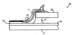
【0023】
図3を参照すれば、本発明の別の実施例によるOLED50の端部の断面図が示されている。以下の説明を簡単にするために、前述のOLED20の要素と同一の機能を果たすOLED50の要素には同一の参照符号が付加されており、それらに関する説明は省略する。このOLED50の場合にも、封止層51は、前述のようにエポキシ層53上に蒸着されたSiNH層52から構成される1つ又は複数の2相層から構築されている。この封止層は、トップカバープレート18上に形成される。封止プロセスにおいては、保護テープ層55を使用して電極16を保護する。このテープ層55は、封止プロセスが完了した後に除去される。
【0024】
この図3の実施例においては、封止層は、カバープレート18の端部周辺にのみ形成されている。但し、OLEDによって生成された光はデバイスの底部を通って出射するため、カバープレートの上面全体に封止層を設けることも可能である。そして、カバープレートの全面に材料を適用する場合には、この層を回転成形によって形成することができる。
【0025】
上述の説明及び添付の図面から当業者には本発明に対する様々な変更が明らかになるであろう。従って、本発明は、添付の請求項の範囲によってのみ限定されるものである。
【0026】
最後に、本発明の代表的な実施態様をまとめて示す。
(実施態様1)
電子発光デバイス(20、50)であって、水分及び酸素不透過性基板(11)と、前記基板(11)上に蒸着された第1電極(12)と、前記第1電極(12)と電気的な接触状態にある電子発光層(13)と、前記電子発光層と電気的な接触状態にある第2電極(14)と、エポキシ層(21)上に位置するシリコン窒化物の層(22)を有し、前記第2電極(14)に水分及び酸素が到達するのを防止する封止部材とを有することを特徴とする電子発光デバイス(20、50)。
【0027】
(実施態様2)
前記エポキシ層は、前記第2電極(14)をカバーすることを特徴とする実施態様1記載の電子発光デバイス(20、50)。
【0028】
(実施態様3)
前記封止部材は、水分及び酸素不透過性のプレート(18)を更に有することを特徴とする実施態様1記載の電子発光デバイス(20、50)。
【0029】
(実施態様4)
前記エポキシ(21)は、140℃未満の硬化温度を有することを特徴とする実施態様1記載の電子発光デバイス(20、50)。
【0030】
(実施態様5)
前記エポキシ(21)は、無水物のエポキシを有することを特徴とする実施態様1記載の電子発光デバイス(20、50)。
【0031】
(実施態様6)
前記エポキシ(21)は、ベンゾシクロブテンを有することを特徴とする実施態様1記載の電子発光デバイス(20、50)。
【0032】
(実施態様7)
前記シリコン窒化物層(22)は、10%のHF溶液において50A/秒未満のエッチングレートを有することを特徴とする実施態様1記載の電子発光デバイス(20、50)。
【0033】
(実施態様8)
電子発光デバイス(20、50)の製造方法であって、水分及び酸素不透過性基板(11)上に第1電極(12)を蒸着するステップと、前記第1電極(12)と電気的に接触した状態の電子発光層(13)を蒸着するステップと、前記電子発光層(13)と電気的に接触した状態の第2電極(14)を蒸着するステップと、前記第2電極(14)上に、エポキシ層(21)と該エポキシ層(21)と接触した状態のシリコン窒化物層(22)を有する水分及び酸素不透過性の封止部材を製造するステップとを有することを特徴とする電子発光デバイス(20、50)を製造する方法。
【0034】
(実施態様9)
前記エポキシ層(21)は、前記第2電極(14)上に前記エポキシ(21)をスピンキャスティングによって形成されることを特徴とする実施態様8記載の方法。
【0035】
(実施態様10)
前記エポキシ層(21)は、前記シリコン窒化物層(22)を蒸着する前に140℃未満の温度で硬化されることを特徴とする実施態様8記載の方法。
【0036】
(実施態様11)
前記封止部材は、端部が前記エポキシ(21)及びシリコン窒化物(22)層によって封止された水分及び酸素不透過性のプレート(18)を有することを特徴とする実施態様8記載の方法。
【0037】
(実施態様12)
前記エポキシ(21)は、無水物のエポキシを有することを特徴とする実施態様8記載の方法。
【0038】
(実施態様13)
前記エポキシ(21)は、ベンゾシクロブテンを有することを特徴とする実施態様8記載の方法。
【0039】
(実施態様14)
前記SiNH層は、10%のHF溶液において50A/秒未満のエッチングレートを有することを特徴とする実施態様8記載の方法。
【図面の簡単な説明】
【図1】従来技術によるOLED10の断面図である。
【図2】本発明の一実施例によるOLED20の断面図である。
【図3】本発明の別の実施例によるOLED50の端部の断面図である。
【符号の説明】
20、50 電子発光デバイス
11 基板
12 第1電極
13 電子発光層
14 第2電極
21 エポキシ層
22 シリコン窒化物層
18 プレート[0001]
BACKGROUND OF THE INVENTION
The present invention relates to electroluminescent devices, and more particularly to an improved method for encapsulating organic light emitting displays to extend the lifetime of the display.
[0002]
[Prior art]
Organic light-emitting devices (OLEDs) consist of a transparent substrate coated with a transparent conductive material such as indium oxide and tin (ITO), one or more organic layers, and a metal with low work function characteristics such as Ca and Mg. It is a radioactive display comprised from the cathode manufactured by vaporizing or sputtering. The organic layer is selected such that charge injection and transport from both electrodes to the electroluminescent organic layer (EL) is performed, and charges are recombined in the electroluminescent organic layer to emit light. There is one or more organic hole transport layers (HTL) between the ITO and the EL, and one or more electron injection and transport layers between the cathode and the EL.
[0003]
OLED promises to provide an inexpensive display. However, in order to function over a long period of time, the OLED must be sealed so that moisture and oxygen do not reach the cathode and polymer layer. That is, a cathode metal having a small work function is easily oxidized when exposed to moisture and oxygen. And once oxidized, the cathode metal can no longer function as a charge injector, resulting in a decrease in OLED light output due to high resistance and low electron injection efficiency.
[0004]
One way to improve the resistance of an OLED to moisture is to provide a barrier to moisture by adding a stable metal layer, such as aluminum, on a cathode with a low work function. But unfortunately the protection this kind of barrier provides is not enough.
[0005]
A second prior art method for preventing moisture damage utilizes a package having a back cover made of metal or glass. This back cover is usually bonded to the substrate on which the OLED is manufactured with an epoxy adhesive. Unfortunately, however, epoxy adhesives do not provide sufficient protection against moisture. Therefore, a moisture adsorbing material is sandwiched between the substrate and the back cover in order to further protect the cathode metal from moisture. The moisture adsorbent absorbs the moisture that has passed through the epoxy adhesive before reaching the cathode metal. However, there are two problems with moisture adsorbents. First, the moisture adsorbent has a saturation point at which the efficacy disappears. That is, the adsorbent can only protect the OLED for a certain period. Secondly, the moisture absorbed by the adsorbent is released when the package is heated, resulting in oxidation of the cathode metal.
[0006]
Another method for providing a moisture barrier for use in a flexible OLED is disclosed in US Pat. According to this method, a flexible substrate is coated with a moisture barrier having a structure in which polymer layers sandwiched between inorganic dielectric (nitride or oxide) layers are stacked in layers. However, this method requires the creation of a very smooth polymer layer on which the dielectric is deposited, and the presence of imperfect parts in the polymer layer creates pinholes in the inorganic layer, which is an advanced feature of this type of layer. The blocking performance is greatly reduced.
[0007]
[Patent Document 1]
US Pat. No. 6,146,225 specification
[Problems to be solved by the invention]
Broadly speaking, it is an object of the present invention to provide an improved sealing system for OLEDs and similar structures.
[0009]
This and other objects of the invention will become apparent from the following detailed description of the invention and the accompanying drawings.
[0010]
[Means for Solving the Problems]
The present invention is an electroluminescent device and a method for manufacturing the same. The electroluminescent device includes a moisture and oxygen impermeable substrate having a first electrode. The electroluminescent layer is in electrical contact with the first electrode, and the second electrode is in electrical contact with the electroluminescent layer. A sealing member having an epoxy layer and a silicon nitride layer prevents moisture and oxygen from reaching the second electrode. The epoxy preferably has a curing temperature of less than 140 ° C. Similarly, the SiNH layer is preferably deposited at a temperature below 140 ° C. The SiNH layer preferably has an etching rate of less than 50 A / second in a 10% HF solution.
[0011]
The manner in which the present invention provides its advantages can be easily understood by referring to FIG. 1, which shows a cross-sectional view of an
[0012]
Next, the
[0013]
The cathode and organic layers must be protected against both oxygen and moisture. That is, a cathode metal having a small work function is easily oxidized when exposed to moisture and oxygen. Once oxidized, the cathode metal can no longer function as a charge injector and the light output of the OLED is reduced due to high resistance and low electron injection efficiency.
[0014]
The
[0015]
DETAILED DESCRIPTION OF THE INVENTION
Referring now to FIG. 2, a cross-sectional view of an
[0016]
SiNH films are also used in wafer processing steps, but the deposition temperature used in wafer processing steps exceeds the highest temperature available in OLED manufacturing. That is, in the wafer processing step, the SiNH layer is typically deposited by plasma enhanced chemical vapor deposition (PECVD) at a deposition temperature in the range of 300 to 400 ° C. On the other hand, the polymer LED device utilizes a polyfluorene-based compound and has a glass transition temperature of about 120 to 135 ° C. When the OLED is heated to a temperature above this glass transition temperature, the polymer film will go through an undesirable relaxed state. Therefore, the SiNH layer must be deposited at a temperature below that normally used in semiconductor manufacturing.
[0017]
In principle, low temperature SiNH films can be deposited by various methods including PECVD, high density plasma enhanced chemical vapor deposition, sputtering, and vaporization. The preferred embodiment of the present invention utilizes the PECVD method. In general, the properties of SiNH films deposited by PECVD depend on the gas mixture, pressure, temperature, and high frequency power and frequency.
[0018]
The barrier properties against moisture of these high deposition temperature SiNH films are well known in the art, but the moisture barrier properties at the molecular level are not well understood. That is, there is little knowledge in the art regarding the optimization of the aforementioned parameters to provide a sufficient moisture barrier at low deposition temperatures. The present invention is based on the observation that a SiNH film having a high packing density provides a superior moisture barrier compared to a film having a low packing density.
[0019]
The packing density of the SiNH film can be estimated from the etching rate and refractive index in thin HF. The SiNH film has a refractive index in the range of 1.7 to 2.3 depending on the silicon / nitrogen ratio and the hydrogen content. For a given Si / N ratio, the etch rate in the HF solution is a rough measure of the packing density of the film, indicating that the lower the etching rate, the higher the packing density. In the preferred embodiment of the present invention, the deposition conditions are optimized to provide a refractive index in the range of 1.8 to 2.0 and an etch rate of less than 50 A / second with a 10% HF solution. This can be achieved by an appropriate ratio of silane and nitrogen gas and sufficient ion irradiation when depositing the film. In general, the deposition conditions differ depending on the reactor used. In the case of the reactor in this example, the range of conditions is 500-1000 sccm argon (including 2% silane), 1000-2000 sccm nitrogen, 700-1200 mTorr, 20-80 watts, 100-130 ° C. Although other conditions may be available in other reactors.
[0020]
In the present invention, SiNH is vapor-deposited on the epoxy layer formed on the cathode layer. The epoxy layer can be formed by any general means, and in the preferred embodiment of the present invention, the epoxy layer is formed by rotational molding. The epoxy is cured by heat, UV, or microwave radiation, depending on the epoxy system utilized.
[0021]
In a preferred embodiment of the present invention, the epoxy layer has a clear epoxy / anhydride system with a thickness of about 2 μm and a glass transition temperature of about 140 ° C. The epoxy is cured at 125 ° C. for 2 hours. A suitable epoxy composition is PT5-42, Pacific Polytech Incorporated located in Novato, California. However, other thermosetting polymers that can be crosslinked at temperatures below 130 ° C. may be utilized. Polyimide, polyester, polyurethane, or polyisocyanate based polymers can be utilized. For example, benzocyclobutene having a thickness of about 2 μm can be utilized, and this material is used in wafer processing.
[0022]
In the above embodiments of the present invention, a sealing layer is used, and the cathode is encapsulated by an epoxy and SiNH sealing layer. However, it is also possible to apply this sealing layer to the end of a moisture and oxygen impermeable cover plate. Such an embodiment mitigates chemical interactions between the cathode material and the epoxy layer. This type of embodiment also has the effect of shielding the OLED layer from heat in the vapor deposition process, so that a slightly higher temperature can be utilized without damaging the OLED.
[0023]
Referring to FIG. 3, a cross-sectional view of the end of an
[0024]
In the embodiment of FIG. 3, the sealing layer is formed only around the end of the
[0025]
Various modifications to the present invention will become apparent to those skilled in the art from the foregoing description and accompanying drawings. Accordingly, the invention is limited only by the scope of the appended claims.
[0026]
Finally, representative embodiments of the present invention are summarized.
(Embodiment 1)
An electroluminescent device (20, 50), a moisture and oxygen impermeable substrate (11), a first electrode (12) deposited on the substrate (11), and the first electrode (12) An electroluminescent layer (13) in electrical contact, a second electrode (14) in electrical contact with the electroluminescent layer, and a silicon nitride layer (on the epoxy layer (21)) 22) and a sealing member for preventing moisture and oxygen from reaching the second electrode (14).
[0027]
(Embodiment 2)
2. The electroluminescent device (20, 50) according to embodiment 1, wherein the epoxy layer covers the second electrode (14).
[0028]
(Embodiment 3)
The electroluminescent device (20, 50) according to embodiment 1, wherein the sealing member further comprises a moisture and oxygen impermeable plate (18).
[0029]
(Embodiment 4)
The electroluminescent device (20, 50) according to embodiment 1, wherein the epoxy (21) has a curing temperature of less than 140 ° C.
[0030]
(Embodiment 5)
The electroluminescent device (20, 50) according to embodiment 1, wherein the epoxy (21) comprises an anhydride epoxy.
[0031]
(Embodiment 6)
The electroluminescent device (20, 50) according to embodiment 1, wherein the epoxy (21) comprises benzocyclobutene.
[0032]
(Embodiment 7)
2. The electroluminescent device (20, 50) according to embodiment 1, wherein the silicon nitride layer (22) has an etching rate of less than 50 A / sec in a 10% HF solution.
[0033]
(Embodiment 8)
A method of manufacturing an electroluminescent device (20, 50), comprising: depositing a first electrode (12) on a moisture and oxygen impermeable substrate (11); and electrically connecting the first electrode (12) Depositing the contacted electroluminescent layer (13); depositing the second electrode (14) in electrical contact with the electroluminescent layer (13); and the second electrode (14). And manufacturing a moisture and oxygen impermeable sealing member having an epoxy layer (21) and a silicon nitride layer (22) in contact with the epoxy layer (21). A method of manufacturing an electroluminescent device (20, 50).
[0034]
(Embodiment 9)
The method according to claim 8, wherein the epoxy layer (21) is formed by spin casting the epoxy (21) on the second electrode (14).
[0035]
(Embodiment 10)
9. The method of embodiment 8, wherein the epoxy layer (21) is cured at a temperature below 140 ° C. prior to depositing the silicon nitride layer (22).
[0036]
(Embodiment 11)
9. The embodiment of claim 8, wherein the sealing member comprises a moisture and oxygen impermeable plate (18) whose ends are sealed by the epoxy (21) and silicon nitride (22) layers. Method.
[0037]
(Embodiment 12)
Embodiment 9. The method of embodiment 8, wherein the epoxy (21) comprises an anhydride epoxy.
[0038]
(Embodiment 13)
Embodiment 9. The method of embodiment 8, wherein the epoxy (21) comprises benzocyclobutene.
[0039]
(Embodiment 14)
9. The method of embodiment 8, wherein the SiNH layer has an etch rate of less than 50 A / second in a 10% HF solution.
[Brief description of the drawings]
FIG. 1 is a cross-sectional view of an
FIG. 2 is a cross-sectional view of an
FIG. 3 is a cross-sectional view of an end portion of an
[Explanation of symbols]
20, 50
Claims (12)
水分及び酸素不透過性基板(11)と、
前記基板(11)上に蒸着された第1電極(12)と、
前記第1電極(12)と電気的な接触状態にある電子発光層(13)と、
前記電子発光層と電気的な接触状態にある第2電極(14)と、
エポキシ層(21)上に位置するSiNH層(22)を含んで成り、前記第2電極(14)に水分及び酸素が到達するのを防止する封止部材と、
を有し、
前記SiNH層(22)は、1.8〜2.0の範囲の屈折率及び10%のHF溶液における50Å/秒未満のエッチングレートを有する、電子発光デバイス(20、50)。An electroluminescent device (20, 50) comprising:
A moisture and oxygen impermeable substrate (11);
A first electrode (12) deposited on the substrate (11);
An electroluminescent layer (13) in electrical contact with the first electrode (12);
A second electrode (14) in electrical contact with the electroluminescent layer;
A sealing member comprising a SiNH layer (22) positioned on the epoxy layer (21) and preventing moisture and oxygen from reaching the second electrode (14);
I have a,
The electroluminescent device (20, 50), wherein the SiNH layer (22) has a refractive index in the range of 1.8-2.0 and an etching rate of less than 50 / sec in a 10% HF solution .
水分及び酸素不透過性基板(11)上に第1電極(12)を蒸着するステップと、
前記第1電極(12)と電気的に接触した状態の電子発光層(13)を蒸着するステップと、
前記電子発光層(13)と電気的に接触した状態の第2電極(14)を蒸着するステップと、
前記第2電極(14)上に、エポキシ層(21)と該エポキシ層(21)と接触した状態のSiNH層(22)を有する水分及び酸素不透過性の封止部材を製造するステップと、
を有し、
前記SiNH層は、1.8〜2.0の範囲の屈折率及び10%のHF溶液における50Å/秒未満のエッチングレートを有する、電子発光デバイス(20、50)を製造する方法。A method for manufacturing an electroluminescent device (20, 50) comprising:
Depositing a first electrode (12) on a moisture and oxygen impermeable substrate (11);
Depositing an electroluminescent layer (13) in electrical contact with the first electrode (12);
Depositing a second electrode (14) in electrical contact with the electroluminescent layer (13);
Manufacturing a moisture and oxygen impermeable sealing member having an epoxy layer (21) and a SiNH layer (22) in contact with the epoxy layer (21) on the second electrode (14);
I have a,
A method of manufacturing an electroluminescent device (20, 50), wherein the SiNH layer has a refractive index in the range of 1.8-2.0 and an etching rate of less than 50 / sec in a 10% HF solution .
Applications Claiming Priority (1)
| Application Number | Priority Date | Filing Date | Title |
|---|---|---|---|
| US10/212,638 US6710542B2 (en) | 2002-08-03 | 2002-08-03 | Organic light emitting device with improved moisture seal |
Publications (3)
| Publication Number | Publication Date |
|---|---|
| JP2004071549A JP2004071549A (en) | 2004-03-04 |
| JP2004071549A5 JP2004071549A5 (en) | 2006-08-31 |
| JP4456343B2 true JP4456343B2 (en) | 2010-04-28 |
Family
ID=31187814
Family Applications (1)
| Application Number | Title | Priority Date | Filing Date |
|---|---|---|---|
| JP2003196333A Expired - Fee Related JP4456343B2 (en) | 2002-08-03 | 2003-07-14 | Organic light emitting device and manufacturing method |
Country Status (2)
| Country | Link |
|---|---|
| US (1) | US6710542B2 (en) |
| JP (1) | JP4456343B2 (en) |
Families Citing this family (40)
| Publication number | Priority date | Publication date | Assignee | Title |
|---|---|---|---|---|
| US7198832B2 (en) * | 1999-10-25 | 2007-04-03 | Vitex Systems, Inc. | Method for edge sealing barrier films |
| US6866901B2 (en) * | 1999-10-25 | 2005-03-15 | Vitex Systems, Inc. | Method for edge sealing barrier films |
| US20100330748A1 (en) | 1999-10-25 | 2010-12-30 | Xi Chu | Method of encapsulating an environmentally sensitive device |
| JP4776769B2 (en) * | 1999-11-09 | 2011-09-21 | 株式会社半導体エネルギー研究所 | Method for manufacturing light emitting device |
| US7301276B2 (en) * | 2000-03-27 | 2007-11-27 | Semiconductor Energy Laboratory Co., Ltd. | Light emitting apparatus and method of manufacturing the same |
| US6924594B2 (en) * | 2000-10-03 | 2005-08-02 | Semiconductor Energy Laboratory Co., Ltd. | Light emitting device |
| TW548860B (en) | 2001-06-20 | 2003-08-21 | Semiconductor Energy Lab | Light emitting device and method of manufacturing the same |
| US7211828B2 (en) * | 2001-06-20 | 2007-05-01 | Semiconductor Energy Laboratory Co., Ltd. | Light emitting device and electronic apparatus |
| US7109653B2 (en) * | 2002-01-15 | 2006-09-19 | Seiko Epson Corporation | Sealing structure with barrier membrane for electronic element, display device, electronic apparatus, and fabrication method for electronic element |
| US8900366B2 (en) * | 2002-04-15 | 2014-12-02 | Samsung Display Co., Ltd. | Apparatus for depositing a multilayer coating on discrete sheets |
| US8808457B2 (en) * | 2002-04-15 | 2014-08-19 | Samsung Display Co., Ltd. | Apparatus for depositing a multilayer coating on discrete sheets |
| US7230271B2 (en) | 2002-06-11 | 2007-06-12 | Semiconductor Energy Laboratory Co., Ltd. | Light emitting device comprising film having hygroscopic property and transparency and manufacturing method thereof |
| GB0223510D0 (en) * | 2002-10-10 | 2002-11-13 | Cambridge Display Tech Ltd | Optical device |
| US7535017B2 (en) * | 2003-05-30 | 2009-05-19 | Osram Opto Semiconductors Gmbh | Flexible multilayer packaging material and electronic devices with the packaging material |
| US6982480B2 (en) * | 2003-07-31 | 2006-01-03 | The Boeing Company | Near hermetic packaging of gallium arsenide semiconductor devices and manufacturing method therefor |
| JP2007535144A (en) * | 2004-04-22 | 2007-11-29 | オスラム オプト セミコンダクターズ ゲゼルシャフト ミット ベシュレンクテル ハフツング | Encapsulation for organic electronic devices, fabrication method of encapsulation and use of encapsulation |
| US20090093074A1 (en) * | 2004-04-23 | 2009-04-09 | Jae Hyung Yi | Light Emission From Silicon-Based Nanocrystals By Sequential Thermal Annealing Approaches |
| US7202504B2 (en) | 2004-05-20 | 2007-04-10 | Semiconductor Energy Laboratory Co., Ltd. | Light-emitting element and display device |
| US7214600B2 (en) * | 2004-06-25 | 2007-05-08 | Applied Materials, Inc. | Method to improve transmittance of an encapsulating film |
| JP5848862B2 (en) | 2004-06-25 | 2016-01-27 | アプライド マテリアルズ インコーポレイテッドApplied Materials,Incorporated | Improving the water shielding performance of the encapsulated membrane |
| US7220687B2 (en) * | 2004-06-25 | 2007-05-22 | Applied Materials, Inc. | Method to improve water-barrier performance by changing film surface morphology |
| JP2006049308A (en) * | 2004-08-04 | 2006-02-16 | Samsung Electronics Co Ltd | Display device, manufacturing method of the same, and manufacturing device for the same |
| US7915822B2 (en) * | 2004-08-04 | 2011-03-29 | Samsung Electronics Co., Ltd. | Display device and method and apparatus for manufacturing the same |
| JP4631683B2 (en) * | 2005-01-17 | 2011-02-16 | セイコーエプソン株式会社 | Light emitting device and electronic device |
| JP2006222071A (en) * | 2005-01-17 | 2006-08-24 | Seiko Epson Corp | Light emitting device, manufacturing method thereof, and electronic equipment |
| JP4539368B2 (en) * | 2005-02-24 | 2010-09-08 | ソニー株式会社 | Manufacturing method of display device |
| EP1804310B1 (en) * | 2005-12-30 | 2016-10-19 | Samsung Display Co., Ltd. | Organic light emiting device and method of manufacturing the same |
| US20080100202A1 (en) * | 2006-11-01 | 2008-05-01 | Cok Ronald S | Process for forming oled conductive protective layer |
| JP5208591B2 (en) | 2007-06-28 | 2013-06-12 | 株式会社半導体エネルギー研究所 | Light emitting device and lighting device |
| DE102008033017A1 (en) * | 2008-07-14 | 2010-01-21 | Osram Opto Semiconductors Gmbh | Encapsulated optoelectronic component and method for its production |
| US9337446B2 (en) | 2008-12-22 | 2016-05-10 | Samsung Display Co., Ltd. | Encapsulated RGB OLEDs having enhanced optical output |
| US9184410B2 (en) | 2008-12-22 | 2015-11-10 | Samsung Display Co., Ltd. | Encapsulated white OLEDs having enhanced optical output |
| US20100167002A1 (en) * | 2008-12-30 | 2010-07-01 | Vitex Systems, Inc. | Method for encapsulating environmentally sensitive devices |
| US8590338B2 (en) | 2009-12-31 | 2013-11-26 | Samsung Mobile Display Co., Ltd. | Evaporator with internal restriction |
| JP5452266B2 (en) * | 2010-02-08 | 2014-03-26 | パナソニック株式会社 | Light emitting device |
| JP2014150001A (en) * | 2013-02-01 | 2014-08-21 | Nitto Denko Corp | Organic electroluminescent device |
| US9287522B2 (en) | 2013-07-30 | 2016-03-15 | Global Oled Technology Llc | Local seal for encapsulation of electro-optical element on a flexible substrate |
| US9494792B2 (en) | 2013-07-30 | 2016-11-15 | Global Oled Technology Llc | Local seal for encapsulation of electro-optical element on a flexible substrate |
| US9385342B2 (en) | 2013-07-30 | 2016-07-05 | Global Oled Technology Llc | Local seal for encapsulation of electro-optical element on a flexible substrate |
| KR102415052B1 (en) * | 2015-09-18 | 2022-07-01 | 삼성디스플레이 주식회사 | Organic light emitting display device and method of manufacturing an organic light emitting display device |
Family Cites Families (5)
| Publication number | Priority date | Publication date | Assignee | Title |
|---|---|---|---|---|
| US5491377A (en) * | 1993-08-03 | 1996-02-13 | Janusauskas; Albert | Electroluminescent lamp and method |
| US6049167A (en) * | 1997-02-17 | 2000-04-11 | Tdk Corporation | Organic electroluminescent display device, and method and system for making the same |
| JP2845239B1 (en) * | 1997-12-17 | 1999-01-13 | 日本電気株式会社 | Organic thin film EL device and manufacturing method thereof |
| JP2000208255A (en) * | 1999-01-13 | 2000-07-28 | Nec Corp | Organic electroluminescent display and manufacture thereof |
| DE10152655B4 (en) * | 2000-10-17 | 2013-10-02 | Samsung Display Co., Ltd. | Process for producing an organic electroluminescent device |
-
2002
- 2002-08-03 US US10/212,638 patent/US6710542B2/en not_active Expired - Lifetime
-
2003
- 2003-07-14 JP JP2003196333A patent/JP4456343B2/en not_active Expired - Fee Related
Also Published As
| Publication number | Publication date |
|---|---|
| US6710542B2 (en) | 2004-03-23 |
| US20040021416A1 (en) | 2004-02-05 |
| JP2004071549A (en) | 2004-03-04 |
Similar Documents
| Publication | Publication Date | Title |
|---|---|---|
| JP4456343B2 (en) | Organic light emitting device and manufacturing method | |
| US9601721B2 (en) | Encapsulation for an organic electronic device | |
| JP4856313B2 (en) | Environmental barrier material for organic light emitting device and method of manufacturing the same | |
| US20050174045A1 (en) | Organic light-emitting device display having a plurality of passive polymer layers | |
| US9515288B2 (en) | Organic electroluminescent device | |
| US8350470B2 (en) | Encapsulation structures of organic electroluminescence devices | |
| US20060061272A1 (en) | Organic electroluminescent device | |
| WO2005101542A1 (en) | Encapsulating oled devices | |
| KR20140048243A (en) | Organic optoelectronic device and method for the encapsulation thereof | |
| JP2006501607A (en) | Passivation layer | |
| KR20140026647A (en) | Encapsulation structure for an opto-electronic component, and method for encapsulating an optoelectronic component | |
| US20040056269A1 (en) | Passivation structure | |
| KR101995337B1 (en) | Organic light emitting display and fabricating method of the same | |
| JP5980343B2 (en) | Method for manufacturing optoelectronic device | |
| US20050158454A1 (en) | Method and system for forming an organic light-emitting device display having a plurality of passive polymer layers | |
| CN111725422A (en) | Display panel, preparation method thereof and display device | |
| JP2004342515A (en) | Sealing structure | |
| US8044583B2 (en) | Organic electroluminescent device without cap and getter | |
| JP5079967B2 (en) | Plasma encapsulation for electronic and microelectronic structural elements such as OLEDs | |
| US9153794B2 (en) | Thin film encapsulation of organic light emitting diodes | |
| US6103541A (en) | Encapsulation method of an organic electroluminescent device | |
| KR101218651B1 (en) | Organic light emitting device and method for the same | |
| JP5163619B2 (en) | Sealing structure | |
| KR102373437B1 (en) | Organic light emitting device and manufacturing method the same | |
| US20050127822A1 (en) | Electroluminescence device |
Legal Events
| Date | Code | Title | Description |
|---|---|---|---|
| A521 | Request for written amendment filed |
Free format text: JAPANESE INTERMEDIATE CODE: A523 Effective date: 20060713 |
|
| A621 | Written request for application examination |
Free format text: JAPANESE INTERMEDIATE CODE: A621 Effective date: 20060713 |
|
| RD03 | Notification of appointment of power of attorney |
Free format text: JAPANESE INTERMEDIATE CODE: A7423 Effective date: 20060713 |
|
| A711 | Notification of change in applicant |
Free format text: JAPANESE INTERMEDIATE CODE: A711 Effective date: 20070326 |
|
| A131 | Notification of reasons for refusal |
Free format text: JAPANESE INTERMEDIATE CODE: A131 Effective date: 20090609 |
|
| A521 | Request for written amendment filed |
Free format text: JAPANESE INTERMEDIATE CODE: A523 Effective date: 20090908 |
|
| A131 | Notification of reasons for refusal |
Free format text: JAPANESE INTERMEDIATE CODE: A131 Effective date: 20091006 |
|
| A521 | Request for written amendment filed |
Free format text: JAPANESE INTERMEDIATE CODE: A523 Effective date: 20100106 |
|
| TRDD | Decision of grant or rejection written | ||
| A01 | Written decision to grant a patent or to grant a registration (utility model) |
Free format text: JAPANESE INTERMEDIATE CODE: A01 Effective date: 20100202 |
|
| A01 | Written decision to grant a patent or to grant a registration (utility model) |
Free format text: JAPANESE INTERMEDIATE CODE: A01 |
|
| A61 | First payment of annual fees (during grant procedure) |
Free format text: JAPANESE INTERMEDIATE CODE: A61 Effective date: 20100205 |
|
| FPAY | Renewal fee payment (event date is renewal date of database) |
Free format text: PAYMENT UNTIL: 20130212 Year of fee payment: 3 |
|
| R150 | Certificate of patent or registration of utility model |
Free format text: JAPANESE INTERMEDIATE CODE: R150 |
|
| FPAY | Renewal fee payment (event date is renewal date of database) |
Free format text: PAYMENT UNTIL: 20130212 Year of fee payment: 3 |
|
| S111 | Request for change of ownership or part of ownership |
Free format text: JAPANESE INTERMEDIATE CODE: R313113 |
|
| FPAY | Renewal fee payment (event date is renewal date of database) |
Free format text: PAYMENT UNTIL: 20130212 Year of fee payment: 3 |
|
| R350 | Written notification of registration of transfer |
Free format text: JAPANESE INTERMEDIATE CODE: R350 |
|
| FPAY | Renewal fee payment (event date is renewal date of database) |
Free format text: PAYMENT UNTIL: 20140212 Year of fee payment: 4 |
|
| R250 | Receipt of annual fees |
Free format text: JAPANESE INTERMEDIATE CODE: R250 |
|
| R250 | Receipt of annual fees |
Free format text: JAPANESE INTERMEDIATE CODE: R250 |
|
| R250 | Receipt of annual fees |
Free format text: JAPANESE INTERMEDIATE CODE: R250 |
|
| R250 | Receipt of annual fees |
Free format text: JAPANESE INTERMEDIATE CODE: R250 |
|
| LAPS | Cancellation because of no payment of annual fees |