JP4446891B2 - Vertical stacked pore phase change memory - Google Patents
Vertical stacked pore phase change memory Download PDFInfo
- Publication number
- JP4446891B2 JP4446891B2 JP2004560263A JP2004560263A JP4446891B2 JP 4446891 B2 JP4446891 B2 JP 4446891B2 JP 2004560263 A JP2004560263 A JP 2004560263A JP 2004560263 A JP2004560263 A JP 2004560263A JP 4446891 B2 JP4446891 B2 JP 4446891B2
- Authority
- JP
- Japan
- Prior art keywords
- phase change
- layer
- change material
- bottom electrode
- hole
- Prior art date
- Legal status (The legal status is an assumption and is not a legal conclusion. Google has not performed a legal analysis and makes no representation as to the accuracy of the status listed.)
- Expired - Fee Related
Links
Images

Classifications
-
- H—ELECTRICITY
- H10—SEMICONDUCTOR DEVICES; ELECTRIC SOLID-STATE DEVICES NOT OTHERWISE PROVIDED FOR
- H10N—ELECTRIC SOLID-STATE DEVICES NOT OTHERWISE PROVIDED FOR
- H10N70/00—Solid-state devices without a potential-jump barrier or surface barrier, and specially adapted for rectifying, amplifying, oscillating or switching
- H10N70/20—Multistable switching devices, e.g. memristors
- H10N70/231—Multistable switching devices, e.g. memristors based on solid-state phase change, e.g. between amorphous and crystalline phases, Ovshinsky effect
-
- G—PHYSICS
- G11—INFORMATION STORAGE
- G11C—STATIC STORES
- G11C13/00—Digital stores characterised by the use of storage elements not covered by groups G11C11/00, G11C23/00, or G11C25/00
- G11C13/0002—Digital stores characterised by the use of storage elements not covered by groups G11C11/00, G11C23/00, or G11C25/00 using resistive RAM [RRAM] elements
- G11C13/0021—Auxiliary circuits
- G11C13/0069—Writing or programming circuits or methods
-
- H—ELECTRICITY
- H10—SEMICONDUCTOR DEVICES; ELECTRIC SOLID-STATE DEVICES NOT OTHERWISE PROVIDED FOR
- H10B—ELECTRONIC MEMORY DEVICES
- H10B63/00—Resistance change memory devices, e.g. resistive RAM [ReRAM] devices
- H10B63/20—Resistance change memory devices, e.g. resistive RAM [ReRAM] devices comprising selection components having two electrodes, e.g. diodes
-
- H—ELECTRICITY
- H10—SEMICONDUCTOR DEVICES; ELECTRIC SOLID-STATE DEVICES NOT OTHERWISE PROVIDED FOR
- H10N—ELECTRIC SOLID-STATE DEVICES NOT OTHERWISE PROVIDED FOR
- H10N70/00—Solid-state devices without a potential-jump barrier or surface barrier, and specially adapted for rectifying, amplifying, oscillating or switching
- H10N70/011—Manufacture or treatment of multistable switching devices
- H10N70/061—Patterning of the switching material
-
- H—ELECTRICITY
- H10—SEMICONDUCTOR DEVICES; ELECTRIC SOLID-STATE DEVICES NOT OTHERWISE PROVIDED FOR
- H10N—ELECTRIC SOLID-STATE DEVICES NOT OTHERWISE PROVIDED FOR
- H10N70/00—Solid-state devices without a potential-jump barrier or surface barrier, and specially adapted for rectifying, amplifying, oscillating or switching
- H10N70/801—Constructional details of multistable switching devices
- H10N70/821—Device geometry
- H10N70/826—Device geometry adapted for essentially vertical current flow, e.g. sandwich or pillar type devices
-
- H—ELECTRICITY
- H10—SEMICONDUCTOR DEVICES; ELECTRIC SOLID-STATE DEVICES NOT OTHERWISE PROVIDED FOR
- H10N—ELECTRIC SOLID-STATE DEVICES NOT OTHERWISE PROVIDED FOR
- H10N70/00—Solid-state devices without a potential-jump barrier or surface barrier, and specially adapted for rectifying, amplifying, oscillating or switching
- H10N70/801—Constructional details of multistable switching devices
- H10N70/841—Electrodes
- H10N70/8413—Electrodes adapted for resistive heating
-
- H—ELECTRICITY
- H10—SEMICONDUCTOR DEVICES; ELECTRIC SOLID-STATE DEVICES NOT OTHERWISE PROVIDED FOR
- H10N—ELECTRIC SOLID-STATE DEVICES NOT OTHERWISE PROVIDED FOR
- H10N70/00—Solid-state devices without a potential-jump barrier or surface barrier, and specially adapted for rectifying, amplifying, oscillating or switching
- H10N70/801—Constructional details of multistable switching devices
- H10N70/881—Switching materials
- H10N70/882—Compounds of sulfur, selenium or tellurium, e.g. chalcogenides
- H10N70/8828—Tellurides, e.g. GeSbTe
-
- G—PHYSICS
- G11—INFORMATION STORAGE
- G11C—STATIC STORES
- G11C13/00—Digital stores characterised by the use of storage elements not covered by groups G11C11/00, G11C23/00, or G11C25/00
- G11C13/0002—Digital stores characterised by the use of storage elements not covered by groups G11C11/00, G11C23/00, or G11C25/00 using resistive RAM [RRAM] elements
- G11C13/0021—Auxiliary circuits
- G11C13/0069—Writing or programming circuits or methods
- G11C2013/008—Write by generating heat in the surroundings of the memory material, e.g. thermowrite
-
- G—PHYSICS
- G11—INFORMATION STORAGE
- G11C—STATIC STORES
- G11C2213/00—Indexing scheme relating to G11C13/00 for features not covered by this group
- G11C2213/50—Resistive cell structure aspects
- G11C2213/52—Structure characterized by the electrode material, shape, etc.
-
- Y—GENERAL TAGGING OF NEW TECHNOLOGICAL DEVELOPMENTS; GENERAL TAGGING OF CROSS-SECTIONAL TECHNOLOGIES SPANNING OVER SEVERAL SECTIONS OF THE IPC; TECHNICAL SUBJECTS COVERED BY FORMER USPC CROSS-REFERENCE ART COLLECTIONS [XRACs] AND DIGESTS
- Y10—TECHNICAL SUBJECTS COVERED BY FORMER USPC
- Y10T—TECHNICAL SUBJECTS COVERED BY FORMER US CLASSIFICATION
- Y10T428/00—Stock material or miscellaneous articles
- Y10T428/13—Hollow or container type article [e.g., tube, vase, etc.]
Landscapes
- Engineering & Computer Science (AREA)
- Manufacturing & Machinery (AREA)
- Semiconductor Memories (AREA)
- Inert Electrodes (AREA)
- Battery Electrode And Active Subsutance (AREA)
Description
本発明は、概して電子メモリに関し、特に相変化材料を用いる電子メモリに関する。 The present invention relates generally to electronic memories, and more particularly to electronic memories using phase change materials.
相変化材料は、少なくとも2種類の状態を持ち、これらの状態は、アモルファス状態および結晶質状態と呼ばれる。両状態間の遷移は、選択的に生じさせることができる。通常アモルファス状態は、結晶質状態よりも高い抵抗を示すため、両状態を区別することができる。アモルファス状態では、より不規則な原子構造となる。通常は、いずれの相変化材料を利用しても良い。ただし、薄膜カルコゲナイド合金材料を用いることが好ましい場合がある。 Phase change materials have at least two states, which are referred to as an amorphous state and a crystalline state. Transitions between both states can occur selectively. Usually, the amorphous state shows higher resistance than the crystalline state, so that both states can be distinguished. In the amorphous state, the atomic structure becomes more irregular. Usually, any phase change material may be used. However, it may be preferable to use a thin film chalcogenide alloy material.
相変化は可逆的に生じる。すなわちメモリには、温度の変化に応じてアモルファスから結晶質状態に変化し、その後結晶質からアモルファス状態に戻る変化、あるいはその逆の変化が生じ得る。実際には、各メモリセルはプログラム化レジスタとみなすことができ、メモリセルは、高抵抗と低抵抗の状態間で可逆的に変化する。相変化は抵抗加熱によって生じる。 The phase change occurs reversibly. That is, the memory may change from an amorphous state to a crystalline state in response to a change in temperature, and then change from the crystalline state to the amorphous state, or vice versa. In practice, each memory cell can be viewed as a programmed register, and the memory cell reversibly changes between a high resistance and a low resistance state. The phase change is caused by resistance heating.
相変化メモリにおいては、相変化材料の加熱が非効率的であることが示されている。従って相変化材料の加熱を適切に行うことに対してニーズがある。 In phase change memory, heating of the phase change material has been shown to be inefficient. Therefore, there is a need for properly heating the phase change material.
本発明は、相変化材料の加熱をより均一に行うことの可能な相変化メモリ、およびその製作方法を提供することを課題とする。 An object of the present invention is to provide a phase change memory capable of more uniformly heating a phase change material and a method for manufacturing the same.
本発明のある態様では、
絶縁体、
該絶縁体上の相変化材料、
該相変化材料に結合された底部電極であって、低抵抗層の上部に高抵抗層を有する底部電極、
とを有する相変化メモリが提供される。
In one aspect of the present invention,
Insulator,
A phase change material on the insulator;
A bottom electrode coupled to the phase change material, the bottom electrode having a high resistance layer on top of the low resistance layer;
A phase change memory is provided.
本発明のメモリにおいて、前記高抵抗層は、前記層変化材料に接続されても良い。 In the memory of the present invention, the high resistance layer may be connected to the layer change material.
また前記低抵抗層は、前記高抵抗層よりも薄くすることができる。 The low resistance layer can be made thinner than the high resistance layer.
さらに本発明のメモリは、前記低抵抗層に接続されたカップ状導体を有しても良い。 Furthermore, the memory of the present invention may have a cup-shaped conductor connected to the low resistance layer.
さらに本発明のメモリは、前記相変化材料の層と前記底部電極の間に絶縁体を有し、該絶縁体内には孔部が形成されても良い。 Furthermore, the memory of the present invention may have an insulator between the layer of phase change material and the bottom electrode, and a hole may be formed in the insulator.
本発明の別の態様では、
第1の層および第2の層を有する底部電極を形成するステップであって、前記第2の層は、前記第1の層より高い抵抗率を有する、ステップと、
前記第2の層の上部に相変化材料を形成するステップと、
を有する方法が提供される。
In another aspect of the invention,
Forming a bottom electrode having a first layer and a second layer, wherein the second layer has a higher resistivity than the first layer; and
Forming a phase change material on top of the second layer;
Is provided.
本発明の方法は、前記第2の層を導体と接続させるステップを有しても良い。 The method of the present invention may comprise the step of connecting the second layer with a conductor.
また本発明の方法は、前記底部電極の上部に絶縁体を形成するステップおよび前記絶縁体に孔部を形成するステップを有しても良い。 The method of the present invention may further include a step of forming an insulator on the bottom electrode and a step of forming a hole in the insulator.
さらに本発明の方法は、前記孔部内に、前記底部電極と接続された前記相変化材料を形成するステップを有しても良い。 The method of the present invention may further include forming the phase change material connected to the bottom electrode in the hole.
さらに本発明の方法は、前記孔部よりも幅の広い底部電極を形成するステップを有しても良い。 Furthermore, the method of the present invention may include a step of forming a bottom electrode wider than the hole.
本発明のさらに別の態様では、
孔部を定形する絶縁層と、
前記孔部に設置された相変化材料と、
前記相変化材料と接続するように前記孔部の底部に設置された底部電極と、
を有する相変化メモリであって、前記底部電極は第1および第2の層を有し、前記第1の層は前記相変化材料と接続され、前記第2の層よりも高い抵抗率を有することを特徴とする、相変化メモリが提供される。
In yet another aspect of the invention,
An insulating layer that shapes the hole;
A phase change material installed in the hole;
A bottom electrode installed at the bottom of the hole to connect with the phase change material;
Wherein the bottom electrode has first and second layers, the first layer is connected to the phase change material and has a higher resistivity than the second layer. A phase change memory is provided.
本発明のメモリにおいては、前記第2の層は、前記第1の層よりも薄くすることができる。 In the memory of the present invention, the second layer can be made thinner than the first layer.
また本発明のメモリは、前記第2の層に接続されたカップ状導体を有しても良い。 The memory of the present invention may have a cup-shaped conductor connected to the second layer.
さらに本発明のメモリにおいては、前記底部電極は、前記孔部より幅が広くても良い。 Furthermore, in the memory of the present invention, the bottom electrode may be wider than the hole.
図1には、複数の相変化メモリセル12からなる相変化メモリ10が示されており、メモリセルには、隣接するビットライン14における隣接セル12aおよび12bが含まれる。各ビットライン14は、バリア材16上に設置される。バリア材16は、相変化材料18の上部に設置され、一部は孔部に向かって延びる。本発明の実施例では、相変化材料はカルコゲナイド材料である。
FIG. 1 shows a phase change memory 10 made up of a plurality of phase change memory cells 12, which includes
本実施例では、これに限定されるものではないが、相変化メモリ材料は、テレリウム−ゲルマニウム−アンチモン(TexGeySbz)材料またはGeSbTe合金のようなカルコゲナイド成分を有する。ただし本発明の範囲はこれに限定されるものではない。代わりに電気特性(例えば抵抗、容量等)がエネルギーの印加、例えば光、熱または電流等によって変化するような、別の相変化材料を用いても良い。 In this embodiment, the phase change memory material has a chalcogenide component such as a telelium-germanium-antimony (TexGeySbz) material or a GeSbTe alloy, although not limited thereto. However, the scope of the present invention is not limited to this. Alternatively, other phase change materials may be used whose electrical properties (eg, resistance, capacitance, etc.) are changed by the application of energy, eg, light, heat or current.
ある実施例では孔部46は、側壁スペーサ22によって定形される。孔部46および側壁スペーサ22は、誘電体または絶縁体の材料20内に形成された開口によって定形されても良い。材料20は、酸化物、窒化物または他のいかなる絶縁材料であっても良い。 In one embodiment, the hole 46 is shaped by the sidewall spacer 22. The holes 46 and the sidewall spacers 22 may be shaped by openings formed in the dielectric or insulator material 20. Material 20 may be an oxide, nitride, or any other insulating material.
孔部46の下には、1組の底部電極が設置され、この電極組は、比較的高抵抗の底部電極24と、比較的低抵抗の底部電極26とを有する。高抵抗電極24は、相変化材料46と隣接する箇所を加熱する役割を有し、垂直方向の厚さは厚い。低抵抗電極26は、高抵抗電極24の幅全体にわたって横断する電流を十分に分散させる役割を有する。
Under the hole 46, a set of bottom electrodes is installed, and this electrode set includes a bottom electrode 24 having a relatively high resistance and a
ある実施例では、電流は、低抵抗電極26から台座状導体30を介して流れる。本発明のある実施例では、導体30は、中に絶縁体28が充填されたカップ状であって、絶縁体28は、さらに台座状導体30を取り囲む。
In one embodiment, current flows from the
台座状導体30は、窒化物層32を貫通している。窒化物層32は、絶縁層35上部に設置される。なお絶縁層35は、p+領域38を有する半導体基板上に形成される。
The pedestal-
p+領域38は、シリサイド接触領域34と隣接しても良い。p+領域の下には、n型シリコン層40が存在する。n+領域36は、隣接ビットライン14の間に設置される。本発明のある実施例では、n型シリコン層40の底部には、p型エピタキシャル(EPI)シリコン層42とp++型シリコン基板44が存在する。
The p +
高抵抗底部電極24の抵抗は、1乃至500mΩ-cmであるが、30乃至100mΩ-cmの範囲であることが好ましい。本発明のある実施例では、低抵抗底部電極26は、0.01乃至1.0mΩ-cmの抵抗率であって、0.05乃至0.15mΩ-cmであることが好ましい。電極26に用いられる低抵抗材料の例として、例えば、窒化タンタルが挙げられる。
The resistance of the high resistance bottom electrode 24 is 1 to 500 mΩ-cm, but is preferably in the range of 30 to 100 mΩ-cm. In one embodiment of the present invention, the low
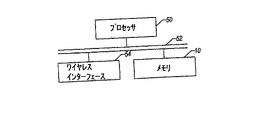
図2に示されているプロセッサを基本とするシステムは、プロセッサ50を有し、このプロセッサは、2例を挙げると、通常の目的のプロセッサまたはデジタル信号プロセッサである。プロセッサ50は、例えばバス52によってメモリ10に結合される。ある実施例では、ワイヤレスインターフェース54が提供される。ワイヤレスインターフェース54は、例えばトランシーバまたはアンテナを有する。 The processor-based system shown in FIG. 2 includes a processor 50, which is a general purpose processor or a digital signal processor, to name two examples. The processor 50 is coupled to the memory 10 by a bus 52, for example. In certain embodiments, a wireless interface 54 is provided. The wireless interface 54 includes, for example, a transceiver or an antenna.
本発明は、限定された数の実施例で説明されたが、多くの変更や修正が可能であることは、当業者には明らかであろう。添付の請求項には、本発明の概念および範囲内にあるそのような変更や修正が含まれる。 While the invention has been described in a limited number of embodiments, it will be apparent to those skilled in the art that many changes and modifications can be made. The appended claims include such changes and modifications that are within the spirit and scope of the present invention.
Claims (12)
該相変化材料に結合された底部電極であって、低抵抗層の上部に高抵抗層を有する底部電極、
を有する相変化メモリであって、
前記底部電極は、相変化材料を含まず、前記低抵抗層は、前記高抵抗層よりも薄く、
前記高抵抗層は、前記相変化材料と隣接する箇所を加熱する役割を有することを特徴とする相変化メモリ。A phase change material, and a bottom electrode coupled to the phase change material, the bottom electrode having a high resistance layer on top of the low resistance layer;
A phase change memory having
The bottom electrode does not include a phase change material, and the low resistance layer is thinner than the high resistance layer,
The phase change memory according to claim 1, wherein the high resistance layer has a role of heating a portion adjacent to the phase change material.
前記第2の層の上部に相変化材料を形成するステップと、
を有し、
前記底部電極は、相変化材料を含まず、前記第1の層は、前記第2の層よりも薄く、
前記第2の層は、前記相変化材料と隣接する箇所を加熱する役割を有することを特徴とする方法。Forming a bottom electrode having a first layer and a second layer, wherein the second layer has a higher resistivity than the first layer; and
Forming a phase change material on top of the second layer;
Have
The bottom electrode does not include a phase change material, the first layer is thinner than the second layer,
The method of claim 2, wherein the second layer serves to heat a portion adjacent to the phase change material.
前記孔部に設置された相変化材料と、
前記相変化材料と接続するように前記孔部の底部に設置された底部電極と、
を有する相変化メモリであって、前記底部電極は第1および第2の層を有し、前記第1の層は前記相変化材料と接続され、前記第2の層よりも高い抵抗率を有し、
前記底部電極は、相変化材料を含まず、前記第2の層は、前記第1の層よりも薄く、
前記第1の層は、前記相変化材料と隣接する箇所を加熱する役割を有することを特徴とする、相変化メモリ。An insulating layer that shapes the hole;
A phase change material installed in the hole;
A bottom electrode installed at the bottom of the hole to connect with the phase change material;
The bottom electrode has first and second layers, and the first layer is connected to the phase change material and has a higher resistivity than the second layer. And
The bottom electrode does not include a phase change material, and the second layer is thinner than the first layer,
The phase change memory according to claim 1, wherein the first layer has a role of heating a portion adjacent to the phase change material.
Applications Claiming Priority (2)
| Application Number | Priority Date | Filing Date | Title |
|---|---|---|---|
| US10/319,179 US7049623B2 (en) | 2002-12-13 | 2002-12-13 | Vertical elevated pore phase change memory |
| PCT/US2003/013360 WO2004055915A2 (en) | 2002-12-13 | 2003-04-28 | Vertical elevated pore phase change memory |
Publications (3)
| Publication Number | Publication Date |
|---|---|
| JP2006510219A JP2006510219A (en) | 2006-03-23 |
| JP2006510219A5 JP2006510219A5 (en) | 2009-05-14 |
| JP4446891B2 true JP4446891B2 (en) | 2010-04-07 |
Family
ID=32506588
Family Applications (1)
| Application Number | Title | Priority Date | Filing Date |
|---|---|---|---|
| JP2004560263A Expired - Fee Related JP4446891B2 (en) | 2002-12-13 | 2003-04-28 | Vertical stacked pore phase change memory |
Country Status (8)
| Country | Link |
|---|---|
| US (2) | US7049623B2 (en) |
| JP (1) | JP4446891B2 (en) |
| KR (1) | KR100669312B1 (en) |
| CN (1) | CN1714461B (en) |
| AU (1) | AU2003225226A1 (en) |
| MY (1) | MY135245A (en) |
| TW (1) | TWI286750B (en) |
| WO (1) | WO2004055915A2 (en) |
Families Citing this family (47)
| Publication number | Priority date | Publication date | Assignee | Title |
|---|---|---|---|---|
| EP1331675B1 (en) * | 2002-01-17 | 2007-05-23 | STMicroelectronics S.r.l. | Integrated resistive element, phase-change memory element including said resistive element, and method of manufacture thereof |
| US7425735B2 (en) | 2003-02-24 | 2008-09-16 | Samsung Electronics Co., Ltd. | Multi-layer phase-changeable memory devices |
| US7115927B2 (en) | 2003-02-24 | 2006-10-03 | Samsung Electronics Co., Ltd. | Phase changeable memory devices |
| US7402851B2 (en) * | 2003-02-24 | 2008-07-22 | Samsung Electronics Co., Ltd. | Phase changeable memory devices including nitrogen and/or silicon and methods for fabricating the same |
| US7211819B2 (en) * | 2003-08-04 | 2007-05-01 | Intel Corporation | Damascene phase change memory |
| US7943919B2 (en) * | 2003-12-10 | 2011-05-17 | International Business Machines Corporation | Integrated circuit with upstanding stylus |
| KR100668824B1 (en) * | 2004-06-30 | 2007-01-16 | 주식회사 하이닉스반도체 | Phase-change memory device and method for manufacturing the same |
| KR100668823B1 (en) * | 2004-06-30 | 2007-01-16 | 주식회사 하이닉스반도체 | Phase-change memory device and method for manufacturing the same |
| KR100623181B1 (en) * | 2004-08-23 | 2006-09-19 | 삼성전자주식회사 | Phase-changeable memory device and method of manufacturing the same |
| KR100568543B1 (en) * | 2004-08-31 | 2006-04-07 | 삼성전자주식회사 | Method of forming a phase change memory device having a small area of contact |
| JP2006303294A (en) * | 2005-04-22 | 2006-11-02 | Renesas Technology Corp | Variable-phase nonvolatile memory and its manufacturing method |
| US7408240B2 (en) * | 2005-05-02 | 2008-08-05 | Infineon Technologies Ag | Memory device |
| US20060255328A1 (en) * | 2005-05-12 | 2006-11-16 | Dennison Charles H | Using conductive oxidation for phase change memory electrodes |
| KR100650735B1 (en) * | 2005-05-26 | 2006-11-27 | 주식회사 하이닉스반도체 | Phase change ram device and method of manufacturing the same |
| KR100687747B1 (en) * | 2005-07-29 | 2007-02-27 | 한국전자통신연구원 | Phase change type memory device and method of manufacturing the same |
| KR100687750B1 (en) * | 2005-09-07 | 2007-02-27 | 한국전자통신연구원 | Phase change type memory device using sb-se metal alloy and method of manufacturing the same |
| JP4860249B2 (en) * | 2005-11-26 | 2012-01-25 | エルピーダメモリ株式会社 | Phase change memory device and method of manufacturing phase change memory device |
| JP4860248B2 (en) * | 2005-11-26 | 2012-01-25 | エルピーダメモリ株式会社 | Phase change memory device and method of manufacturing phase change memory device |
| US8896045B2 (en) * | 2006-04-19 | 2014-11-25 | Infineon Technologies Ag | Integrated circuit including sidewall spacer |
| KR100722769B1 (en) * | 2006-05-19 | 2007-05-30 | 삼성전자주식회사 | Phase-change memory device and method of manufacturing the same |
| KR100782482B1 (en) * | 2006-05-19 | 2007-12-05 | 삼성전자주식회사 | Phase change memory cell employing a GeBiTe layer as a phase change material layer, phase change memory device including the same, electronic device including the same and method of fabricating the same |
| US7696077B2 (en) * | 2006-07-14 | 2010-04-13 | Micron Technology, Inc. | Bottom electrode contacts for semiconductor devices and methods of forming same |
| JP4437299B2 (en) | 2006-08-25 | 2010-03-24 | エルピーダメモリ株式会社 | Semiconductor device and manufacturing method thereof |
| US8003972B2 (en) | 2006-08-30 | 2011-08-23 | Micron Technology, Inc. | Bottom electrode geometry for phase change memory |
| US7511984B2 (en) | 2006-08-30 | 2009-03-31 | Micron Technology, Inc. | Phase change memory |
| KR100810615B1 (en) * | 2006-09-20 | 2008-03-06 | 삼성전자주식회사 | Phase change memory device having high temp phase change pattern and method of fabricating the same |
| US7388771B2 (en) * | 2006-10-24 | 2008-06-17 | Macronix International Co., Ltd. | Methods of operating a bistable resistance random access memory with multiple memory layers and multilevel memory states |
| US8067762B2 (en) | 2006-11-16 | 2011-11-29 | Macronix International Co., Ltd. | Resistance random access memory structure for enhanced retention |
| US8426967B2 (en) * | 2007-01-05 | 2013-04-23 | International Business Machines Corporation | Scaled-down phase change memory cell in recessed heater |
| US20080164453A1 (en) * | 2007-01-07 | 2008-07-10 | Breitwisch Matthew J | Uniform critical dimension size pore for pcram application |
| KR101350979B1 (en) * | 2007-05-11 | 2014-01-14 | 삼성전자주식회사 | Resistive memory device and Manufacturing Method for the same |
| KR100911473B1 (en) * | 2007-06-18 | 2009-08-11 | 삼성전자주식회사 | Phase-change memory unit, method of forming the phase-change memory unit, phase-change memory device having the phase-change memory unit and method of manufacturing the phase-change memory device |
| KR100881055B1 (en) * | 2007-06-20 | 2009-01-30 | 삼성전자주식회사 | Phase-change memory unit, method of forming the phase-change memory unit, phase-change memory device having the phase-change memory unit and method of manufacturing the phase-change memory device |
| US7863593B2 (en) * | 2007-07-20 | 2011-01-04 | Qimonda Ag | Integrated circuit including force-filled resistivity changing material |
| US9018615B2 (en) * | 2007-08-03 | 2015-04-28 | Macronix International Co., Ltd. | Resistor random access memory structure having a defined small area of electrical contact |
| US7760546B2 (en) * | 2008-02-28 | 2010-07-20 | Qimonda North America Corp. | Integrated circuit including an electrode having an outer portion with greater resistivity |
| JP2009206418A (en) * | 2008-02-29 | 2009-09-10 | Elpida Memory Inc | Nonvolatile memory device and manufacturing method for the same |
| JP2009212202A (en) * | 2008-03-03 | 2009-09-17 | Elpida Memory Inc | Phase change memory device and fabrication method thereof |
| US7848139B2 (en) * | 2008-09-18 | 2010-12-07 | Seagate Technology Llc | Memory device structures including phase-change storage cells |
| KR20100084215A (en) * | 2009-01-16 | 2010-07-26 | 삼성전자주식회사 | Phase change memory device having barrier protective layer silicicd bottom electrode and method for manufacturing same |
| US9190609B2 (en) * | 2010-05-21 | 2015-11-17 | Entegris, Inc. | Germanium antimony telluride materials and devices incorporating same |
| US8574954B2 (en) | 2010-08-31 | 2013-11-05 | Micron Technology, Inc. | Phase change memory structures and methods |
| WO2014070682A1 (en) | 2012-10-30 | 2014-05-08 | Advaned Technology Materials, Inc. | Double self-aligned phase change memory device structure |
| US9112148B2 (en) | 2013-09-30 | 2015-08-18 | Taiwan Semiconductor Manufacturing Co., Ltd. | RRAM cell structure with laterally offset BEVA/TEVA |
| US9178144B1 (en) | 2014-04-14 | 2015-11-03 | Taiwan Semiconductor Manufacturing Co., Ltd. | RRAM cell with bottom electrode |
| US9209392B1 (en) | 2014-10-14 | 2015-12-08 | Taiwan Semiconductor Manufacturing Co., Ltd. | RRAM cell with bottom electrode |
| US9741930B2 (en) * | 2015-03-27 | 2017-08-22 | Intel Corporation | Materials and components in phase change memory devices |
Family Cites Families (11)
| Publication number | Priority date | Publication date | Assignee | Title |
|---|---|---|---|---|
| US5414271A (en) * | 1991-01-18 | 1995-05-09 | Energy Conversion Devices, Inc. | Electrically erasable memory elements having improved set resistance stability |
| US5534711A (en) * | 1991-01-18 | 1996-07-09 | Energy Conversion Devices, Inc. | Electrically erasable, directly overwritable, multibit single cell memory elements and arrays fabricated therefrom |
| US5789758A (en) * | 1995-06-07 | 1998-08-04 | Micron Technology, Inc. | Chalcogenide memory cell with a plurality of chalcogenide electrodes |
| US6653733B1 (en) * | 1996-02-23 | 2003-11-25 | Micron Technology, Inc. | Conductors in semiconductor devices |
| US7173317B1 (en) * | 1998-11-09 | 2007-02-06 | Micron Technology, Inc. | Electrical and thermal contact for use in semiconductor devices |
| US6339544B1 (en) * | 2000-09-29 | 2002-01-15 | Intel Corporation | Method to enhance performance of thermal resistor device |
| US6507061B1 (en) * | 2001-08-31 | 2003-01-14 | Intel Corporation | Multiple layer phase-change memory |
| US6586761B2 (en) * | 2001-09-07 | 2003-07-01 | Intel Corporation | Phase change material memory device |
| US6545287B2 (en) * | 2001-09-07 | 2003-04-08 | Intel Corporation | Using selective deposition to form phase-change memory cells |
| US6566700B2 (en) * | 2001-10-11 | 2003-05-20 | Ovonyx, Inc. | Carbon-containing interfacial layer for phase-change memory |
| US6791102B2 (en) * | 2002-12-13 | 2004-09-14 | Intel Corporation | Phase change memory |
-
2002
- 2002-12-13 US US10/319,179 patent/US7049623B2/en not_active Expired - Lifetime
-
2003
- 2003-04-28 JP JP2004560263A patent/JP4446891B2/en not_active Expired - Fee Related
- 2003-04-28 CN CN03825591.XA patent/CN1714461B/en not_active Expired - Lifetime
- 2003-04-28 KR KR1020057010563A patent/KR100669312B1/en active IP Right Grant
- 2003-04-28 WO PCT/US2003/013360 patent/WO2004055915A2/en active Application Filing
- 2003-04-28 AU AU2003225226A patent/AU2003225226A1/en not_active Abandoned
- 2003-05-09 TW TW092112708A patent/TWI286750B/en not_active IP Right Cessation
- 2003-05-21 MY MYPI20031877A patent/MY135245A/en unknown
-
2005
- 2005-11-10 US US11/270,909 patent/US7364937B2/en not_active Expired - Lifetime
Also Published As
| Publication number | Publication date |
|---|---|
| KR100669312B1 (en) | 2007-01-16 |
| US7049623B2 (en) | 2006-05-23 |
| CN1714461A (en) | 2005-12-28 |
| US20060054878A1 (en) | 2006-03-16 |
| WO2004055915A2 (en) | 2004-07-01 |
| WO2004055915A3 (en) | 2004-08-26 |
| KR20050085526A (en) | 2005-08-29 |
| AU2003225226A1 (en) | 2004-07-09 |
| TWI286750B (en) | 2007-09-11 |
| MY135245A (en) | 2008-03-31 |
| JP2006510219A (en) | 2006-03-23 |
| US20040115372A1 (en) | 2004-06-17 |
| TW200410245A (en) | 2004-06-16 |
| US7364937B2 (en) | 2008-04-29 |
| CN1714461B (en) | 2010-12-08 |
Similar Documents
| Publication | Publication Date | Title |
|---|---|---|
| JP4446891B2 (en) | Vertical stacked pore phase change memory | |
| US9159915B2 (en) | Phase change memory with threshold switch select device | |
| US8377741B2 (en) | Self-heating phase change memory cell architecture | |
| KR101067969B1 (en) | Phase change memory elements using self-aligned phase change material layers and methods of making and using same | |
| JP6059349B2 (en) | 3D memory array architecture | |
| TWI384585B (en) | Variable resistance memory device having reduced bottom contact area and method of forming the same | |
| JP6007255B2 (en) | Memory cell and memory cell array | |
| KR101486984B1 (en) | Resistance changeable memory device and method of forming thereof | |
| US6992365B2 (en) | Reducing leakage currents in memories with phase-change material | |
| US20120220099A1 (en) | Forming a Phase Change Memory With an Ovonic Threshold Switch | |
| KR101051520B1 (en) | Low power consumption phase change memory and its formation method | |
| JP2014523647A (en) | Memory cell structure | |
| KR20040033017A (en) | Phase Change Material Memory Device | |
| JP2007194631A (en) | Resistance memory device equipped with storage node containing noncrystalline solid electrolyte layer | |
| WO2005017906A1 (en) | Multilayered phase change memory | |
| JP2006190941A (en) | Phase change memory and its manufacturing method | |
| US20110309320A1 (en) | Method for active pinch off of an ovonic unified memory element | |
| US20060098524A1 (en) | Forming planarized semiconductor structures | |
| TWI559517B (en) | Sidewall diode driving device and memory using the same | |
| US8680499B2 (en) | Memory cells | |
| TW201709367A (en) | Thermal management structure for low-power nonvolatile filamentary switch | |
| US9059404B2 (en) | Resistive memory with a stabilizer | |
| KR20050059855A (en) | Phase change memory device and method of fabricating the same | |
| CN110867464B (en) | Memristor based on 1T1R structure, preparation method thereof and integrated structure | |
| EP1710850B1 (en) | Lateral phase change memory |
Legal Events
| Date | Code | Title | Description |
|---|---|---|---|
| A977 | Report on retrieval |
Free format text: JAPANESE INTERMEDIATE CODE: A971007 Effective date: 20071017 |
|
| A131 | Notification of reasons for refusal |
Free format text: JAPANESE INTERMEDIATE CODE: A131 Effective date: 20090106 |
|
| A524 | Written submission of copy of amendment under article 19 pct |
Free format text: JAPANESE INTERMEDIATE CODE: A524 Effective date: 20090330 |
|
| A131 | Notification of reasons for refusal |
Free format text: JAPANESE INTERMEDIATE CODE: A131 Effective date: 20090428 |
|
| A521 | Request for written amendment filed |
Free format text: JAPANESE INTERMEDIATE CODE: A523 Effective date: 20090714 |
|
| A131 | Notification of reasons for refusal |
Free format text: JAPANESE INTERMEDIATE CODE: A131 Effective date: 20090901 |
|
| A521 | Request for written amendment filed |
Free format text: JAPANESE INTERMEDIATE CODE: A523 Effective date: 20091127 |
|
| TRDD | Decision of grant or rejection written | ||
| A01 | Written decision to grant a patent or to grant a registration (utility model) |
Free format text: JAPANESE INTERMEDIATE CODE: A01 Effective date: 20100105 |
|
| A01 | Written decision to grant a patent or to grant a registration (utility model) |
Free format text: JAPANESE INTERMEDIATE CODE: A01 |
|
| A61 | First payment of annual fees (during grant procedure) |
Free format text: JAPANESE INTERMEDIATE CODE: A61 Effective date: 20100119 |
|
| FPAY | Renewal fee payment (event date is renewal date of database) |
Free format text: PAYMENT UNTIL: 20130129 Year of fee payment: 3 |
|
| R150 | Certificate of patent or registration of utility model |
Ref document number: 4446891 Country of ref document: JP Free format text: JAPANESE INTERMEDIATE CODE: R150 Free format text: JAPANESE INTERMEDIATE CODE: R150 |
|
| FPAY | Renewal fee payment (event date is renewal date of database) |
Free format text: PAYMENT UNTIL: 20130129 Year of fee payment: 3 |
|
| R250 | Receipt of annual fees |
Free format text: JAPANESE INTERMEDIATE CODE: R250 |
|
| R250 | Receipt of annual fees |
Free format text: JAPANESE INTERMEDIATE CODE: R250 |
|
| R250 | Receipt of annual fees |
Free format text: JAPANESE INTERMEDIATE CODE: R250 |
|
| R250 | Receipt of annual fees |
Free format text: JAPANESE INTERMEDIATE CODE: R250 |
|
| R250 | Receipt of annual fees |
Free format text: JAPANESE INTERMEDIATE CODE: R250 |
|
| R250 | Receipt of annual fees |
Free format text: JAPANESE INTERMEDIATE CODE: R250 |
|
| R250 | Receipt of annual fees |
Free format text: JAPANESE INTERMEDIATE CODE: R250 |
|
| R250 | Receipt of annual fees |
Free format text: JAPANESE INTERMEDIATE CODE: R250 |
|
| R250 | Receipt of annual fees |
Free format text: JAPANESE INTERMEDIATE CODE: R250 |
|
| R250 | Receipt of annual fees |
Free format text: JAPANESE INTERMEDIATE CODE: R250 |
|
| LAPS | Cancellation because of no payment of annual fees |