JP4445258B2 - Stable energy detector for detection of extreme ultraviolet radiation - Google Patents
Stable energy detector for detection of extreme ultraviolet radiation Download PDFInfo
- Publication number
- JP4445258B2 JP4445258B2 JP2003521450A JP2003521450A JP4445258B2 JP 4445258 B2 JP4445258 B2 JP 4445258B2 JP 2003521450 A JP2003521450 A JP 2003521450A JP 2003521450 A JP2003521450 A JP 2003521450A JP 4445258 B2 JP4445258 B2 JP 4445258B2
- Authority
- JP
- Japan
- Prior art keywords
- detector
- euv
- radiation
- detector element
- housing
- Prior art date
- Legal status (The legal status is an assumption and is not a legal conclusion. Google has not performed a legal analysis and makes no representation as to the accuracy of the status listed.)
- Expired - Lifetime
Links
- 230000005855 radiation Effects 0.000 title claims description 54
- 238000001514 detection method Methods 0.000 title claims description 5
- 230000003287 optical effect Effects 0.000 claims description 25
- 238000000926 separation method Methods 0.000 claims description 11
- 238000000034 method Methods 0.000 claims description 10
- 230000008569 process Effects 0.000 claims description 7
- 230000007774 longterm Effects 0.000 claims description 5
- 230000004888 barrier function Effects 0.000 claims description 3
- 230000005540 biological transmission Effects 0.000 claims description 3
- 230000006798 recombination Effects 0.000 claims description 3
- 238000005215 recombination Methods 0.000 claims description 3
- 230000035945 sensitivity Effects 0.000 claims description 3
- 239000011888 foil Substances 0.000 claims description 2
- 238000001914 filtration Methods 0.000 claims 1
- 239000007789 gas Substances 0.000 description 35
- ZXEYZECDXFPJRJ-UHFFFAOYSA-N $l^{3}-silane;platinum Chemical compound [SiH3].[Pt] ZXEYZECDXFPJRJ-UHFFFAOYSA-N 0.000 description 23
- 229910021339 platinum silicide Inorganic materials 0.000 description 22
- 238000010586 diagram Methods 0.000 description 11
- 230000000694 effects Effects 0.000 description 9
- 238000001900 extreme ultraviolet lithography Methods 0.000 description 9
- 230000007246 mechanism Effects 0.000 description 8
- 238000012544 monitoring process Methods 0.000 description 8
- 239000002245 particle Substances 0.000 description 8
- 230000003595 spectral effect Effects 0.000 description 8
- 239000000463 material Substances 0.000 description 7
- 229910052710 silicon Inorganic materials 0.000 description 7
- XUIMIQQOPSSXEZ-UHFFFAOYSA-N Silicon Chemical compound [Si] XUIMIQQOPSSXEZ-UHFFFAOYSA-N 0.000 description 6
- 239000011358 absorbing material Substances 0.000 description 6
- 239000002243 precursor Substances 0.000 description 6
- 239000010703 silicon Substances 0.000 description 6
- 239000007787 solid Substances 0.000 description 6
- XKRFYHLGVUSROY-UHFFFAOYSA-N Argon Chemical compound [Ar] XKRFYHLGVUSROY-UHFFFAOYSA-N 0.000 description 4
- 239000000428 dust Substances 0.000 description 4
- 239000011261 inert gas Substances 0.000 description 4
- 229910052724 xenon Inorganic materials 0.000 description 4
- FHNFHKCVQCLJFQ-UHFFFAOYSA-N xenon atom Chemical compound [Xe] FHNFHKCVQCLJFQ-UHFFFAOYSA-N 0.000 description 4
- 238000001015 X-ray lithography Methods 0.000 description 3
- 239000000356 contaminant Substances 0.000 description 3
- 238000001459 lithography Methods 0.000 description 3
- 238000000206 photolithography Methods 0.000 description 3
- 238000002310 reflectometry Methods 0.000 description 3
- IJGRMHOSHXDMSA-UHFFFAOYSA-N Atomic nitrogen Chemical compound N#N IJGRMHOSHXDMSA-UHFFFAOYSA-N 0.000 description 2
- YZCKVEUIGOORGS-OUBTZVSYSA-N Deuterium Chemical compound [2H] YZCKVEUIGOORGS-OUBTZVSYSA-N 0.000 description 2
- YCKRFDGAMUMZLT-UHFFFAOYSA-N Fluorine atom Chemical compound [F] YCKRFDGAMUMZLT-UHFFFAOYSA-N 0.000 description 2
- WHXSMMKQMYFTQS-UHFFFAOYSA-N Lithium Chemical compound [Li] WHXSMMKQMYFTQS-UHFFFAOYSA-N 0.000 description 2
- 229910052786 argon Inorganic materials 0.000 description 2
- QVGXLLKOCUKJST-UHFFFAOYSA-N atomic oxygen Chemical compound [O] QVGXLLKOCUKJST-UHFFFAOYSA-N 0.000 description 2
- 230000008901 benefit Effects 0.000 description 2
- 229910052790 beryllium Inorganic materials 0.000 description 2
- ATBAMAFKBVZNFJ-UHFFFAOYSA-N beryllium atom Chemical compound [Be] ATBAMAFKBVZNFJ-UHFFFAOYSA-N 0.000 description 2
- 238000000576 coating method Methods 0.000 description 2
- 229910052805 deuterium Inorganic materials 0.000 description 2
- 239000011737 fluorine Substances 0.000 description 2
- 229910052731 fluorine Inorganic materials 0.000 description 2
- 230000004907 flux Effects 0.000 description 2
- 239000001307 helium Substances 0.000 description 2
- 229910052734 helium Inorganic materials 0.000 description 2
- SWQJXJOGLNCZEY-UHFFFAOYSA-N helium atom Chemical compound [He] SWQJXJOGLNCZEY-UHFFFAOYSA-N 0.000 description 2
- 238000003384 imaging method Methods 0.000 description 2
- 230000006872 improvement Effects 0.000 description 2
- 229910052744 lithium Inorganic materials 0.000 description 2
- 238000005259 measurement Methods 0.000 description 2
- 239000000203 mixture Substances 0.000 description 2
- 238000012806 monitoring device Methods 0.000 description 2
- 239000001301 oxygen Substances 0.000 description 2
- 229910052760 oxygen Inorganic materials 0.000 description 2
- 238000012545 processing Methods 0.000 description 2
- 238000010926 purge Methods 0.000 description 2
- 239000000126 substance Substances 0.000 description 2
- 230000002123 temporal effect Effects 0.000 description 2
- 229910018072 Al 2 O 3 Inorganic materials 0.000 description 1
- 230000005461 Bremsstrahlung Effects 0.000 description 1
- VYZAMTAEIAYCRO-UHFFFAOYSA-N Chromium Chemical compound [Cr] VYZAMTAEIAYCRO-UHFFFAOYSA-N 0.000 description 1
- PXGOKWXKJXAPGV-UHFFFAOYSA-N Fluorine Chemical compound FF PXGOKWXKJXAPGV-UHFFFAOYSA-N 0.000 description 1
- ZOKXTWBITQBERF-UHFFFAOYSA-N Molybdenum Chemical compound [Mo] ZOKXTWBITQBERF-UHFFFAOYSA-N 0.000 description 1
- 229910006295 Si—Mo Inorganic materials 0.000 description 1
- 239000006096 absorbing agent Substances 0.000 description 1
- 238000010521 absorption reaction Methods 0.000 description 1
- 230000006978 adaptation Effects 0.000 description 1
- XAGFODPZIPBFFR-UHFFFAOYSA-N aluminium Chemical compound [Al] XAGFODPZIPBFFR-UHFFFAOYSA-N 0.000 description 1
- 229910052782 aluminium Inorganic materials 0.000 description 1
- PNEYBMLMFCGWSK-UHFFFAOYSA-N aluminium oxide Inorganic materials [O-2].[O-2].[O-2].[Al+3].[Al+3] PNEYBMLMFCGWSK-UHFFFAOYSA-N 0.000 description 1
- 238000000149 argon plasma sintering Methods 0.000 description 1
- 230000015572 biosynthetic process Effects 0.000 description 1
- 239000003990 capacitor Substances 0.000 description 1
- 229910010293 ceramic material Inorganic materials 0.000 description 1
- 239000011248 coating agent Substances 0.000 description 1
- 229910021419 crystalline silicon Inorganic materials 0.000 description 1
- 230000000593 degrading effect Effects 0.000 description 1
- 238000013461 design Methods 0.000 description 1
- 230000006866 deterioration Effects 0.000 description 1
- 238000011161 development Methods 0.000 description 1
- 239000003085 diluting agent Substances 0.000 description 1
- 238000010790 dilution Methods 0.000 description 1
- 239000012895 dilution Substances 0.000 description 1
- 238000009826 distribution Methods 0.000 description 1
- 230000005684 electric field Effects 0.000 description 1
- 238000005516 engineering process Methods 0.000 description 1
- 238000011156 evaluation Methods 0.000 description 1
- 230000001747 exhibiting effect Effects 0.000 description 1
- 238000002474 experimental method Methods 0.000 description 1
- 239000010419 fine particle Substances 0.000 description 1
- 239000012530 fluid Substances 0.000 description 1
- PCHJSUWPFVWCPO-UHFFFAOYSA-N gold Chemical compound [Au] PCHJSUWPFVWCPO-UHFFFAOYSA-N 0.000 description 1
- 229910052737 gold Inorganic materials 0.000 description 1
- 239000010931 gold Substances 0.000 description 1
- 239000001257 hydrogen Substances 0.000 description 1
- 229910052739 hydrogen Inorganic materials 0.000 description 1
- 150000002431 hydrogen Chemical class 0.000 description 1
- 239000012535 impurity Substances 0.000 description 1
- 239000012212 insulator Substances 0.000 description 1
- 238000011835 investigation Methods 0.000 description 1
- 238000010849 ion bombardment Methods 0.000 description 1
- 238000005468 ion implantation Methods 0.000 description 1
- 229910052743 krypton Inorganic materials 0.000 description 1
- DNNSSWSSYDEUBZ-UHFFFAOYSA-N krypton atom Chemical compound [Kr] DNNSSWSSYDEUBZ-UHFFFAOYSA-N 0.000 description 1
- 238000004519 manufacturing process Methods 0.000 description 1
- 238000012986 modification Methods 0.000 description 1
- 230000004048 modification Effects 0.000 description 1
- 229910052750 molybdenum Inorganic materials 0.000 description 1
- 239000011733 molybdenum Substances 0.000 description 1
- 229910052754 neon Inorganic materials 0.000 description 1
- GKAOGPIIYCISHV-UHFFFAOYSA-N neon atom Chemical compound [Ne] GKAOGPIIYCISHV-UHFFFAOYSA-N 0.000 description 1
- 229910052758 niobium Inorganic materials 0.000 description 1
- 239000010955 niobium Substances 0.000 description 1
- GUCVJGMIXFAOAE-UHFFFAOYSA-N niobium atom Chemical compound [Nb] GUCVJGMIXFAOAE-UHFFFAOYSA-N 0.000 description 1
- 150000004767 nitrides Chemical class 0.000 description 1
- 229910052757 nitrogen Inorganic materials 0.000 description 1
- 229910052756 noble gas Inorganic materials 0.000 description 1
- 230000036278 prepulse Effects 0.000 description 1
- 230000001737 promoting effect Effects 0.000 description 1
- 230000001681 protective effect Effects 0.000 description 1
- 238000000746 purification Methods 0.000 description 1
- 230000004044 response Effects 0.000 description 1
- 229910052594 sapphire Inorganic materials 0.000 description 1
- 239000010980 sapphire Substances 0.000 description 1
- 238000007789 sealing Methods 0.000 description 1
- 239000004065 semiconductor Substances 0.000 description 1
- -1 silconium Chemical compound 0.000 description 1
- 230000002269 spontaneous effect Effects 0.000 description 1
- 239000000758 substrate Substances 0.000 description 1
- 230000005469 synchrotron radiation Effects 0.000 description 1
- 238000012360 testing method Methods 0.000 description 1
- 238000012546 transfer Methods 0.000 description 1
- 229910052727 yttrium Inorganic materials 0.000 description 1
- VWQVUPCCIRVNHF-UHFFFAOYSA-N yttrium atom Chemical compound [Y] VWQVUPCCIRVNHF-UHFFFAOYSA-N 0.000 description 1
Images


Classifications
-
- G—PHYSICS
- G01—MEASURING; TESTING
- G01J—MEASUREMENT OF INTENSITY, VELOCITY, SPECTRAL CONTENT, POLARISATION, PHASE OR PULSE CHARACTERISTICS OF INFRARED, VISIBLE OR ULTRAVIOLET LIGHT; COLORIMETRY; RADIATION PYROMETRY
- G01J1/00—Photometry, e.g. photographic exposure meter
- G01J1/42—Photometry, e.g. photographic exposure meter using electric radiation detectors
- G01J1/429—Photometry, e.g. photographic exposure meter using electric radiation detectors applied to measurement of ultraviolet light
-
- B—PERFORMING OPERATIONS; TRANSPORTING
- B82—NANOTECHNOLOGY
- B82Y—SPECIFIC USES OR APPLICATIONS OF NANOSTRUCTURES; MEASUREMENT OR ANALYSIS OF NANOSTRUCTURES; MANUFACTURE OR TREATMENT OF NANOSTRUCTURES
- B82Y10/00—Nanotechnology for information processing, storage or transmission, e.g. quantum computing or single electron logic
-
- G—PHYSICS
- G03—PHOTOGRAPHY; CINEMATOGRAPHY; ANALOGOUS TECHNIQUES USING WAVES OTHER THAN OPTICAL WAVES; ELECTROGRAPHY; HOLOGRAPHY
- G03F—PHOTOMECHANICAL PRODUCTION OF TEXTURED OR PATTERNED SURFACES, e.g. FOR PRINTING, FOR PROCESSING OF SEMICONDUCTOR DEVICES; MATERIALS THEREFOR; ORIGINALS THEREFOR; APPARATUS SPECIALLY ADAPTED THEREFOR
- G03F7/00—Photomechanical, e.g. photolithographic, production of textured or patterned surfaces, e.g. printing surfaces; Materials therefor, e.g. comprising photoresists; Apparatus specially adapted therefor
- G03F7/70—Microphotolithographic exposure; Apparatus therefor
- G03F7/70008—Production of exposure light, i.e. light sources
- G03F7/70033—Production of exposure light, i.e. light sources by plasma extreme ultraviolet [EUV] sources
-
- G—PHYSICS
- G03—PHOTOGRAPHY; CINEMATOGRAPHY; ANALOGOUS TECHNIQUES USING WAVES OTHER THAN OPTICAL WAVES; ELECTROGRAPHY; HOLOGRAPHY
- G03F—PHOTOMECHANICAL PRODUCTION OF TEXTURED OR PATTERNED SURFACES, e.g. FOR PRINTING, FOR PROCESSING OF SEMICONDUCTOR DEVICES; MATERIALS THEREFOR; ORIGINALS THEREFOR; APPARATUS SPECIALLY ADAPTED THEREFOR
- G03F7/00—Photomechanical, e.g. photolithographic, production of textured or patterned surfaces, e.g. printing surfaces; Materials therefor, e.g. comprising photoresists; Apparatus specially adapted therefor
- G03F7/70—Microphotolithographic exposure; Apparatus therefor
- G03F7/70483—Information management; Active and passive control; Testing; Wafer monitoring, e.g. pattern monitoring
- G03F7/7055—Exposure light control in all parts of the microlithographic apparatus, e.g. pulse length control or light interruption
- G03F7/70558—Dose control, i.e. achievement of a desired dose
-
- H—ELECTRICITY
- H01—ELECTRIC ELEMENTS
- H01L—SEMICONDUCTOR DEVICES NOT COVERED BY CLASS H10
- H01L31/00—Semiconductor devices sensitive to infrared radiation, light, electromagnetic radiation of shorter wavelength or corpuscular radiation and specially adapted either for the conversion of the energy of such radiation into electrical energy or for the control of electrical energy by such radiation; Processes or apparatus specially adapted for the manufacture or treatment thereof or of parts thereof; Details thereof
- H01L31/02—Details
- H01L31/0216—Coatings
- H01L31/02161—Coatings for devices characterised by at least one potential jump barrier or surface barrier
- H01L31/02162—Coatings for devices characterised by at least one potential jump barrier or surface barrier for filtering or shielding light, e.g. multicolour filters for photodetectors
-
- H—ELECTRICITY
- H01—ELECTRIC ELEMENTS
- H01L—SEMICONDUCTOR DEVICES NOT COVERED BY CLASS H10
- H01L31/00—Semiconductor devices sensitive to infrared radiation, light, electromagnetic radiation of shorter wavelength or corpuscular radiation and specially adapted either for the conversion of the energy of such radiation into electrical energy or for the control of electrical energy by such radiation; Processes or apparatus specially adapted for the manufacture or treatment thereof or of parts thereof; Details thereof
- H01L31/02—Details
- H01L31/0232—Optical elements or arrangements associated with the device
- H01L31/02325—Optical elements or arrangements associated with the device the optical elements not being integrated nor being directly associated with the device
-
- H—ELECTRICITY
- H01—ELECTRIC ELEMENTS
- H01L—SEMICONDUCTOR DEVICES NOT COVERED BY CLASS H10
- H01L31/00—Semiconductor devices sensitive to infrared radiation, light, electromagnetic radiation of shorter wavelength or corpuscular radiation and specially adapted either for the conversion of the energy of such radiation into electrical energy or for the control of electrical energy by such radiation; Processes or apparatus specially adapted for the manufacture or treatment thereof or of parts thereof; Details thereof
- H01L31/08—Semiconductor devices sensitive to infrared radiation, light, electromagnetic radiation of shorter wavelength or corpuscular radiation and specially adapted either for the conversion of the energy of such radiation into electrical energy or for the control of electrical energy by such radiation; Processes or apparatus specially adapted for the manufacture or treatment thereof or of parts thereof; Details thereof in which radiation controls flow of current through the device, e.g. photoresistors
- H01L31/10—Semiconductor devices sensitive to infrared radiation, light, electromagnetic radiation of shorter wavelength or corpuscular radiation and specially adapted either for the conversion of the energy of such radiation into electrical energy or for the control of electrical energy by such radiation; Processes or apparatus specially adapted for the manufacture or treatment thereof or of parts thereof; Details thereof in which radiation controls flow of current through the device, e.g. photoresistors characterised by at least one potential-jump barrier or surface barrier, e.g. phototransistors
- H01L31/101—Devices sensitive to infrared, visible or ultraviolet radiation
- H01L31/102—Devices sensitive to infrared, visible or ultraviolet radiation characterised by only one potential barrier or surface barrier
- H01L31/103—Devices sensitive to infrared, visible or ultraviolet radiation characterised by only one potential barrier or surface barrier the potential barrier being of the PN homojunction type
- H01L31/1037—Devices sensitive to infrared, visible or ultraviolet radiation characterised by only one potential barrier or surface barrier the potential barrier being of the PN homojunction type the devices comprising active layers formed only by AIVBVI compounds
-
- H—ELECTRICITY
- H01—ELECTRIC ELEMENTS
- H01L—SEMICONDUCTOR DEVICES NOT COVERED BY CLASS H10
- H01L31/00—Semiconductor devices sensitive to infrared radiation, light, electromagnetic radiation of shorter wavelength or corpuscular radiation and specially adapted either for the conversion of the energy of such radiation into electrical energy or for the control of electrical energy by such radiation; Processes or apparatus specially adapted for the manufacture or treatment thereof or of parts thereof; Details thereof
- H01L31/08—Semiconductor devices sensitive to infrared radiation, light, electromagnetic radiation of shorter wavelength or corpuscular radiation and specially adapted either for the conversion of the energy of such radiation into electrical energy or for the control of electrical energy by such radiation; Processes or apparatus specially adapted for the manufacture or treatment thereof or of parts thereof; Details thereof in which radiation controls flow of current through the device, e.g. photoresistors
- H01L31/10—Semiconductor devices sensitive to infrared radiation, light, electromagnetic radiation of shorter wavelength or corpuscular radiation and specially adapted either for the conversion of the energy of such radiation into electrical energy or for the control of electrical energy by such radiation; Processes or apparatus specially adapted for the manufacture or treatment thereof or of parts thereof; Details thereof in which radiation controls flow of current through the device, e.g. photoresistors characterised by at least one potential-jump barrier or surface barrier, e.g. phototransistors
- H01L31/101—Devices sensitive to infrared, visible or ultraviolet radiation
- H01L31/102—Devices sensitive to infrared, visible or ultraviolet radiation characterised by only one potential barrier or surface barrier
- H01L31/108—Devices sensitive to infrared, visible or ultraviolet radiation characterised by only one potential barrier or surface barrier the potential barrier being of the Schottky type
Description
発明の背景
1.発明の技術分野
本発明は、エネルギー監視デバイスに関し、特に、11nmから15nm付近の放射を放出する極紫外放射源のエネルギーの監視に関する。
Background of the Invention TECHNICAL FIELD OF THE INVENTION The present invention relates to energy monitoring devices, and more particularly to monitoring the energy of extreme ultraviolet radiation sources that emit radiation in the vicinity of 11 to 15 nm.
2.関連技術の説明
半導体製造業者は、現在、248nm付近で動作するKrF−エキシマレーザシステムに基づく遠紫外(DUV)リソグラフィ装置を使用し、次世代の装置として193nm付近で動作するArF−エキシマレーザシステムが待望されている。157nm付近で動作するフッ素(F2)レーザは、真空UV(VUV)リソグラフィック処理システムに使用するために開発されている。11nmから15nmの光子ビームを放出する極紫外(EUV)リソグラフィのEUV源または軟X線源も現在開発されている。
2. 2. Description of Related Art Semiconductor manufacturers currently use a deep ultraviolet (DUV) lithographic apparatus based on a KrF-excimer laser system operating near 248 nm, and an ArF-excimer laser system operating near 193 nm is the next generation apparatus. Long-awaited. Fluorine (F 2 ) lasers operating near 157 nm have been developed for use in vacuum UV (VUV) lithographic processing systems. EUV sources or soft X-ray sources for extreme ultraviolet (EUV) lithography that emit 11 to 15 nm photon beams are also currently being developed.
EUV源は有利な出力放射ビームを有し、そのビームは、90eV付近の範囲で光子エネルギーを有する11nmから15nmの波長の光子を含む。フォトリソグラフィを用いて形成可能な最も小さく分解できる形状サイズを表す臨界寸法(CD)が波長に比例するため、この短波長のビームは、フォトリソグラフィの用途に有利である。これにより、より小型で高速なマイクロプロセッサ及び大容量DRAMを一層小型のパッケージに封入することができる。 The EUV source has an advantageous output radiation beam, which contains photons with a wavelength of 11 nm to 15 nm with photon energy in the range around 90 eV. This short wavelength beam is advantageous for photolithography applications because the critical dimension (CD) representing the smallest resolvable feature size that can be formed using photolithography is proportional to wavelength. As a result, a smaller and faster microprocessor and a large-capacity DRAM can be enclosed in a smaller package.
EUVリソグラフィビームを形成する有望な技術は、一組のプラズマピンチ電極を使用し、方位角方向に対称な自己イオン化したプラズマ電子殻をドライブして中心軸に向けて崩壊させる。電源回路は、電極に対して高エネルギー短期間パルスを供給し、数キロボルトの電圧及び百kAまたはそれ以上の電流が1マイクロ秒よりも短いパルス期間に供給される。Z−ピンチ電極回路は、プラズマ電子殻を軸方向に流れる電流を発生し、高速崩壊の要因であるプラズマの荷電粒子に対して径方向の力を与える方位角方向の磁界を発生する。 A promising technique for forming an EUV lithography beam uses a set of plasma pinch electrodes to drive an azimuthally symmetric self-ionized plasma electron shell to collapse towards the central axis. The power supply circuit supplies high energy short duration pulses to the electrodes, with a voltage of a few kilovolts and a current of 100 kA or more supplied in a pulse duration shorter than 1 microsecond. The Z-pinch electrode circuit generates an electric current flowing in the axial direction through the plasma electron shell, and generates an azimuthal magnetic field that applies a radial force to the charged particles of the plasma, which is a cause of fast decay.
エキシマリソグラフィレーザ及びフッ素リソグラフィレーザは、上述したように、レーザ活性ガスの準安定状態に対して反転分布を作り出すガス放電、及び誘電放射を促進するための共振子を用いてレーザビームを放射する。どのような放射メカニズムがプラズマピンチEUV源において軸上の高エネルギー光子放射の原因であるかは、まだ完全には明らかにされていない。プラズマの荷電粒子の殻崩壊により、半径方向の速度により高運動エネルギーが発生する。電子殻の高速崩壊により、中心軸上の新たに生成される殻の全ての部分とこの新たに生成される殻の径方向の反対向きの部分との間で衝突が起こる。 As described above, the excimer lithography laser and the fluorine lithography laser emit a laser beam using a gas discharge that creates an inversion distribution with respect to a metastable state of a laser active gas and a resonator for promoting dielectric emission. It has not yet been fully clarified what radiation mechanism is responsible for the on-axis high energy photon emission in the plasma pinch EUV source. High kinetic energy is generated due to the velocity in the radial direction due to the collapse of the shell of charged particles in the plasma. Due to the fast decay of the electron shell, a collision occurs between all parts of the newly generated shell on the central axis and the radially opposite part of this newly generated shell.
粒子の高運動エネルギーは、X線を放出する高温高密度プラズマに急速に変換される。特に方位角方向に光学的な密度の高くなっているプラズマにより、方位角方向に集中した高再結合速度が提案されており(マルコンマクゴー、極紫外リソグラフィのラジオ周波数の自己イオン化したキセノンのZ−ピンチ源、応用光学、Vol.37、No.9(1998年3月20日)、ここに参考として示す。)、反転分布による自発放射及び顕著な方位角方向の誘導放射、並びに崩壊するプラズマの荷電粒子の軸方向の急速減速することによる制動放射は、高エネルギー光子放出の他のメカニズムである。 The high kinetic energy of the particles is rapidly converted into a high temperature, high density plasma that emits X-rays. A high recombination velocity concentrated in the azimuthal direction has been proposed, particularly due to the plasma with a high optical density in the azimuthal direction (Marcon McGo, ZF of self-ionized xenon at the radio frequency of extreme ultraviolet lithography). -Pinch source, applied optics, Vol. 37, No. 9 (March 20, 1998), shown here for reference), spontaneous emission due to population inversion and stimulated emission in a pronounced azimuthal direction, and decaying plasma The bremsstrahlung by rapid deceleration of the charged particles in the axial direction is another mechanism of high energy photon emission.
過去において、すなわち本出願に導く調査以前には、長期間の157nmレーザパルス放射露光の下でのEUV−光検出器の動作について、ほとんど知られていなかった。さらに、今まで11nm〜15nm付近の波長を有する極紫外ビームのパルスエネルギーを検出するための信頼性のあるエネルギーモニターは利用されていなかった。 In the past, ie prior to the study leading to this application, little was known about the operation of EUV-photodetectors under long-term 157 nm laser pulsed radiation exposure. Furthermore, a reliable energy monitor for detecting the pulse energy of an extreme ultraviolet beam having a wavelength in the vicinity of 11 nm to 15 nm has not been used so far.
193nm及び248nmのエキシマレーザ光を検出するために、インターナショナルラジエーションディテクタ社(IRD)のUVG100(オキシナイトライドカバーを用いたSiフォトダイオード)または浜松ホトニクスのS5226若しくはS1226のようなUV−光検出器は、一般にエネルギー監視検出器として使用されていた。しかしながら、これらの検出器は、EUV光子放射を照射した場合大幅に劣化するおそれがある。 In order to detect 193 nm and 248 nm excimer laser light, UV-light detectors such as International Radiation Detectors (IRD) UVG100 (Si photodiode using oxynitride cover) or Hamamatsu Photonics S5226 or S1226 , Commonly used as an energy monitoring detector. However, these detectors can be significantly degraded when irradiated with EUV photon radiation.
そこで、極紫外放射源のパルスエネルギー及び/または他のパラメータを監視するための信頼性のある光検出器を用いることが望ましい。 It is therefore desirable to use a reliable photodetector for monitoring the pulse energy and / or other parameters of the extreme ultraviolet radiation source.
本発明の概要
上述したように、EUVの照射の下で長寿命の特別な構造のSiベースのフォトダイオードが、EUV放射用の検出器として使用するために提供され、好ましくは他の光学素子と組み合せられる。これらの検出器は、好ましくは、不純物がドープされた不活性領域及び零表面再結合を有するSipnダイオード(Siの不活性領域のダイオード)とすることができる。他の好適な検出器は、PtSiバリア(PtSiフォトダイオード)を有するSipnダイオードである。そのPtSiフォトダイオードもショットキータイプとすることができる。Siの不活性領域のダイオード及びPtSiフォトダイオード検出器の両者は、通常のフォトダイオードを含む検出器に比べて、EUV露光の下で有利な長期間安定性を示す。
SUMMARY OF THE INVENTION As mentioned above, a specially-structured Si-based photodiode that is long-lived under EUV irradiation is provided for use as a detector for EUV radiation, preferably with other optical elements. Can be combined. These detectors may preferably be Sipn diodes (Si inactive region diodes) having an impurity doped inert region and zero surface recombination. Another suitable detector is a Sipn diode with a PtSi barrier (PtSi photodiode). The PtSi photodiode can also be a Schottky type. Both Si inactive region diodes and PtSi photodiode detectors exhibit advantageous long-term stability under EUV exposure compared to detectors containing conventional photodiodes.
0.5nmから10000nmまでの露光波長用の光子検出器(photon detector)として、Siの不活性領域のダイオード及びPtSiフォトダイオードを使用することができる。例えば、それらは、157nmの波長付近で分子フッ素レーザ光の検出器として使用するために説明されている(米国特許出願no.09/771,031を参照、その出願は本出願人に譲り受けられ、ここに参考として示す。)。この波長を用いた長期間テストは、他の調査された検出器(例えば、Si n−p,Si n−pまたはGaAsPショットキーフォトダイオード)に比べて、多くのより優れた安定性を示す。本発明によれば、Siの不活性領域のダイオードまたはPtSiフォトダイオードが、EUVリソグラフィ及び他の用途で、11nmから15nm付近、例えば13.4nm、13.0nmまたは11.5nm付近の波長のEUV放射用の検出器として使用するために提供される。 As photon detectors for exposure wavelengths from 0.5 nm to 10,000 nm, diodes in the Si inactive region and PtSi photodiodes can be used. For example, they have been described for use as detectors of molecular fluorine laser light near a wavelength of 157 nm (see US patent application no. 09 / 771,031, which is assigned to the present applicant, Shown here for reference.) Long term testing using this wavelength shows a lot of better stability compared to other investigated detectors (eg, Si np, Si np or GaAsP Schottky photodiodes). In accordance with the present invention, diodes in the Si inactive region or PtSi photodiodes can be used for EUV lithography and other applications with EUV radiation at a wavelength near 11 to 15 nm, for example near 13.4 nm, 13.0 nm or 11.5 nm. Provided for use as a detector for
多層膜ミラーと独立のフィルターとを組み合せた場合、検出光のスペクトラルレンジは、好適実施例によると、EUV波長領域の注目する小領域に有効に減少する。変形例として、フィルターはダイオード自体の表面上の一方に直接堆積することができる。これにより、フィルターの安定性が高まり、検出器ユニットの処理の複雑さを減少させる。 When a multilayer mirror and an independent filter are combined, the spectral range of the detected light is effectively reduced to a small region of interest in the EUV wavelength region, according to the preferred embodiment. As a variant, the filter can be deposited directly on one of the surfaces of the diode itself. This increases the stability of the filter and reduces the processing complexity of the detector unit.
参考文献の提示
次に、参考文献のサイトリストを示す。それらの参考文献の各々は、上述した参考文献及び以下に示す参考文献に加えて、背景技術として説明されているもの及び上述した発明の概要を含み、これによって、以下に示す詳細な説明の好適実施例に参考文献として組み込まれる。好適実施例の要素または特徴について別の実施例を開示するから、その他の詳細については以下に説明しない。これらの参考文献のうちの単一の文献、または2つ若しくはそれ以上の組み合せを引用して、以下の詳細な説明で説明する好適実施例を変形することができる。さらに、特許、特許出願及び特許でない参考文献の説明が書き示されており、次の参考文献に関して正に説明したように、同一の効果と共に好適実施例の詳細な説明に、参考文献として組み込まれている。
Reference presentation Next, the reference site list is shown. Each of these references includes, in addition to the references mentioned above and the references shown below, what is described as background art and an overview of the invention described above, which makes it suitable for the detailed description given below. Incorporated in the examples as a reference. Since other embodiments are disclosed with respect to elements or features of the preferred embodiments, other details are not described below. The preferred embodiment described in the detailed description below may be modified with reference to a single of these references, or a combination of two or more. In addition, descriptions of patents, patent applications, and non-patent references are written and incorporated as references in the detailed description of the preferred embodiment, with the same effects, as just described for the following references. ing.
K.Solt等,120nmから250nmのスペクトラルレンジの安定したスペクトラル応答速度を用いたPtSi−n−Siショットキー−バリア光検出器,Appl.Phys.Lett69,3662(1996年);
P.S.Shaw等,シンクロトロン放射光を用いた紫外放射線測定及び低温放射線測定,Appl.Optics38,18(1999年);
P.S.Shaw等,NISTのシンクロトロン紫外線設備における新紫外放射測定ビームライン,Metrologia35,301(1998年);
P.Kuschnerus等,120nmから600nmのスペクトラルレンジにおける伝達検出器の規格としてのフォトダイオードの特徴,Metrologla35,355(1998年);
IRDデータシート,SXUVシリーズのフォトダイオード,1999年9月(www.ird-inc.com);
R.Korde等,100%内部量子効率シリコンフォトダイオードにおける1つのギガラド(Gigarad)皮膜保護窒化酸化物,IEEE Transactions on Nuclear Science40,1655(1993年);
L.R.Canfield等,160nmから254nmの光子の絶対シリコンフォトダイオード,Metrologia35,329(1998年);
R.Korde等,紫外線の白金珪化物フロントウィンドウを用いた安定シリコンフォトダイオード,VUV−XII会議での発表;
Malcolm McGeoch,極紫外リソグラフィのラジオ周波数の自己イオン化したキセノンのZ−ピンチ源,Applied Optics,Vol.37,No.9(1998年3月20日);
SPIE3997の議事録,162(2000年);
SEMATECH−ワークショップの議事録,2000年10月,サンフランシスコ;
米国特許no.6,219,368 6,051,841 5,763,930 6,031,241 5,963,616 5,504,795 6,075,838 6,154,470;
ドイツ特許文献no.197 53 696;及び
米国特許出願no.60/281,446,09/512,417,09/598,552,09/712,877,09/594,892,09/131,580,09/317,695,09/738,849,09/718,809,09/771,013,09/693,490及び09/588,561、各米国出願は、本出願人に譲り受けられている。
K. Solt et al., PtSi-n-Si Schottky-barrier photodetector using a stable spectral response speed in the spectral range of 120 nm to 250 nm, Appl. Phys. Lett 69, 3662 (1996);
P. S. Shaw et al., Ultraviolet and low-temperature radiation measurements using synchrotron radiation, Appl. Optics 38, 18 (1999);
P. S. Shaw et al., New Ultraviolet Radiation Measurement Beamline at NIST's Synchrotron UV Facility, Metrologia 35, 301 (1998);
P. Kuschnerus et al., Photodiode features as standard for transfer detectors in the spectral range of 120 nm to 600 nm, Metrologla 35, 355 (1998);
IRD data sheet, SXUV series photodiode, September 1999 (www.ird-inc.com);
R. Korde et al., 1 Gigarad film protective nitride oxide in a 100% internal quantum efficiency silicon photodiode, IEEE Transactions on Nuclear Science 40, 1655 (1993);
L. R. Canfield et al., 160-254 nm photon absolute silicon photodiode, Metrologia 35, 329 (1998);
R. Korde et al., Stable Silicon Photodiode with UV Platinum Silicide Front Window, Presentation at VUV-XII Conference;
Malcolm McGeoch, a radio frequency self-ionized xenon Z-pinch source for extreme ultraviolet lithography, Applied Optics, Vol. 37, no. 9 (March 20, 1998);
Minutes of SPIE 3997, 162 (2000);
Minutes of SEMATECH-Workshop, October 2000, San Francisco;
US patent no. 6,219,368 6,051,841 5,763,930 6,031,241 5,963,616 5,504,795 6,075,838 6,154,470;
German patent document no. 197 53 696; and US patent application no. 60/281, 446, 09/512, 417, 09/598, 552, 09/712, 877, 09/594, 892, 09/131, 580, 09/317, 695, 09/738, 849, 09 / 718,809,09 / 771,013,09 / 693,490 and 09 / 588,561, each of which is assigned to the present applicant.
好適実施例の詳細な説明
好適実施例は、極紫外(EUV)放射を検出するデバイスを含む。極紫外リソグラフィ(EUVL)デバイスについて以下に検討するように、検出される光は、好ましくは、いくつかの多層膜ミラーを含む光学系を透過することができるスペクトラルレンジに制限さる。
DETAILED DESCRIPTION OF PREFERRED EMBODIMENTS Preferred embodiments include devices that detect extreme ultraviolet (EUV) radiation. As discussed below for extreme ultraviolet lithography (EUVL) devices, the detected light is preferably limited to a spectral range that can be transmitted through an optical system that includes several multilayer mirrors.
本発明により、提供されるデバイスを用いて、パルス波または連続波の極紫外(EUV)源のインバンドパワーを計測することができる。インバンドとは、11nmと15nmとの間の波長においていくつかの多層膜ミラーによって反射されるように、約2%のバンド幅の波長領域を表わす。 The present invention allows the in-band power of a pulsed or continuous wave extreme ultraviolet (EUV) source to be measured using the provided device. In-band refers to a wavelength region with a bandwidth of approximately 2% so that it is reflected by several multilayer mirrors at wavelengths between 11 nm and 15 nm.
図1にデバイスの実施例の概略を示す。図1は、単一の多層膜ミラーを含む提案する機構の概略である。EUV源からの光は、多層膜ミラーによって検出器に向けて反射する。その多層膜ミラーは、注目する波長及び放射の入射角に適合して設計される。 FIG. 1 shows an outline of an embodiment of the device. FIG. 1 is a schematic of the proposed mechanism including a single multilayer mirror. Light from the EUV source is reflected toward the detector by the multilayer mirror. The multilayer mirror is designed to match the wavelength of interest and the incident angle of radiation.
検出器自体は、赤外光、可視光、紫外光及びEUV光、並びに硬X線に感応することができる。赤外光、可視光及び紫外光は、1つのまたはそれ以上の不透明なフィルタ、例えば、ベリリウム、ニオブ、シルコニウム、イットリウム及び/または特にシリコンによって好適にフィルタされる。これらのフィルタは、独立の箔またはフォトダイオードの表面に直接堆積した層とすることができる。そのフィルタまたはそれらのフィルタは、長波長側のアウトバンド光を数分の1に減少させる。検出器に入射するX線束は、多層膜ミラー自体によって数分の1に減少する。フィルタ及び多層膜ミラーの組み合せにより、減衰することなく検出器に入射する放射のスペクトラル領域は、EUV波長範囲内にあり、多層膜ミラーの反射特性に依存する。フィルタの厚さを変えることによって及び幾何学的なアブソーバ(例えばメッシュフィルタまたはアパーチャ)を設けることによって、検出器における放射強度を変えることができる。 The detector itself can be sensitive to infrared light, visible light, ultraviolet light and EUV light, and hard X-rays. Infrared light, visible light and ultraviolet light are suitably filtered by one or more opaque filters, such as beryllium, niobium, silconium, yttrium and / or especially silicon. These filters can be independent foils or layers deposited directly on the surface of the photodiode. The filter or those filters reduce the out-band light on the long wavelength side by a fraction. The X-ray flux incident on the detector is reduced to a fraction by the multilayer mirror itself. Due to the combination of the filter and the multilayer mirror, the spectral region of the radiation incident on the detector without attenuation is in the EUV wavelength range and depends on the reflection characteristics of the multilayer mirror. By changing the thickness of the filter and by providing a geometric absorber (eg mesh filter or aperture), the radiation intensity at the detector can be changed.
セットアップにあたり、独立の透過フィルタを組み込んだ検出器としてCCDカメラを用いることができる。例えば、背面照射型CCDカメラを、EUV光に感応する検出器として用いることができる。 In the setup, a CCD camera can be used as a detector incorporating an independent transmission filter. For example, a back-illuminated CCD camera can be used as a detector sensitive to EUV light.
図2に、1組の2つの多層膜ミラーを用いた同様の機構を示す。図2は、1組の2つの多層膜ミラーを用いる提案する機構、及び検出器ユニットの交換可能なモジューラ機構を示す。フィルタ及び減衰器をビームラインに選択的に設けることができる。同様に、2つよりも多いミラーを含む配置構成を用いることができる。2つの多層膜ミラーの反射特性を単一ミラーの反射特性と比較して図3に示す。図3は、単一の多層膜ミラー及び1組の2つの多層膜ミラーにおける計算された反射特性を比較して示している。アウトバンド放射反射は、単一ミラーの反射に比べて大幅に減少され得る。また、反射曲線の幅はより狭く、EUVLデバイスに使用するために計画された光学系全体の反射特性に好適である。両方の効果により、EUVLの用途を考慮して関心のある波長領域についてより正確なEUV信号を得ることができる。 FIG. 2 shows a similar mechanism using a set of two multilayer mirrors. FIG. 2 shows the proposed mechanism using a set of two multilayer mirrors and a replaceable modular mechanism of the detector unit. Filters and attenuators can be selectively provided in the beam line. Similarly, arrangements including more than two mirrors can be used. The reflection characteristics of two multilayer mirrors are shown in FIG. 3 in comparison with the reflection characteristics of a single mirror. FIG. 3 shows a comparison of the calculated reflection characteristics of a single multilayer mirror and a set of two multilayer mirrors. Out-band radiation reflection can be greatly reduced compared to single mirror reflection. Moreover, the width of the reflection curve is narrower, which is suitable for the reflection characteristics of the entire optical system planned for use in an EUVL device. Both effects make it possible to obtain a more accurate EUV signal for the wavelength region of interest in view of EUVL applications.
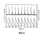
動作原理を図4に示す。図4は、プラズマから発生するレーザを実例にしたデバイスの動作原理を証明する。上側の曲線は、レーザ放射により照射されたフォトダイオードによって発生した信号を示し、下側の信号は、図1に示した検出装置によって発生した信号である。2つの信号の長さは、使用されたフォトダイオードの上昇時間が異なるため、異なっている。 The operating principle is shown in FIG. FIG. 4 demonstrates the principle of operation of a device that demonstrates a laser generated from plasma. The upper curve shows the signal generated by the photodiode irradiated by the laser radiation, and the lower signal is the signal generated by the detection device shown in FIG. The lengths of the two signals are different because the rise times of the used photodiodes are different.
実験用のセットアップでは、EUV源はプラズマからレーザビームを発生させる装置とした。2つの信号は、フォトダイオードにより検出されたレーザパルス(上側の信号)、及び図1に示したデバイスで検出されたEUV信号を示す。 In the experimental setup, the EUV source was a device that generated a laser beam from plasma. The two signals indicate the laser pulse detected by the photodiode (upper signal) and the EUV signal detected by the device shown in FIG.
提案したデバイスの他の有利な特徴は、湾曲面を有する集束性多層膜ミラーを用いることである。これにより、検出器上の光子束を増加させ、モニター機構の感度を向上させることができる。 Another advantageous feature of the proposed device is the use of a focusing multilayer mirror having a curved surface. This can increase the photon flux on the detector and improve the sensitivity of the monitoring mechanism.
ここで好適実施例によれば、EUV源が結合されたビームパラメータモニタリングユニットが提供され、そのEUV源は、11nmから15nm付近の波長を有する出力ビームを発生する。図5から8に線図的に示すそのモニタリングユニットは、ビームスプリッタ、検出器及びビーム路筐体を含む。ビームスプリッタは、出力ビームを第1の成分及び第2の成分に分離するために配置され、第1の成分を用いてワークピースを処理する。本実施例による検出器は、白金シリサイド窓を含み、またはそうでなくてもSiの不活性領域のダイオード(Si dead reagion diode)、PtSi及び特にPtSi−nSiを備え、ビームスプリッタ後の出力ビームの第2の成分の少なくとも1つの光学パラメータを測定する。白金シリサイドの存在により、EUV放射の照射により誘導される検出器の不安定さが減少する。ビーム路筐体は、ビームスプリッタを含むと共に内部素子を有し、レーザリゾネータからビームスプリッタを介して検出器に到る出力ビームの第2の成分の光路は、EUV吸収物質がほとんどないものとなり、その結果第2の成分は光吸収物質によって減衰がほとんど生ずることなく検出器に到達する。 Here, according to a preferred embodiment, a beam parameter monitoring unit coupled with an EUV source is provided, which generates an output beam having a wavelength in the vicinity of 11 nm to 15 nm. The monitoring unit shown diagrammatically in FIGS. 5 to 8 includes a beam splitter, a detector and a beam path housing. The beam splitter is arranged to separate the output beam into a first component and a second component, and processes the workpiece using the first component. The detector according to the present embodiment comprises a platinum silicide window or otherwise comprises a Si dead region diode, PtSi, and in particular PtSi-nSi, for the output beam after the beam splitter. At least one optical parameter of the second component is measured. The presence of platinum silicide reduces detector instability induced by irradiation with EUV radiation. The beam path housing includes a beam splitter and internal elements, and the optical path of the second component of the output beam from the laser resonator to the detector via the beam splitter is almost free of EUV absorbing material, As a result, the second component reaches the detector with little attenuation by the light absorbing material.
図5は、図6から8に関連して以下に説明するように、ビーム路筐体1に結合した検出器ハウジング2内で使用する検出器3の実施例を示す。図5に示した特有な検出器3は、インターナショナルラディエーションディテクターズ(International Radiation Detectors)社により製造され、さらなる情報をwww.ird−inc.comで見つけることができる。そのウェブサイトに掲載された情報をここに参考として示す。ここにおいて、図5に示した検出器がVUV放射の受光に使用するために特に構成され、図5に示した検出器をEUV放射波長の使用に従って変更できることが理解される。
FIG. 5 shows an embodiment of a
図示された検出器3は白金シリサイド(PtSi)窓38を含み、EUV放射の入射によって誘導される検出器3の不安定さを減少させる。検出器の設計に際し、1つ以上のPtSi層を含むことができる。白金シリサイド層を他の場所に配置することができ、例えば、デバイスの一つまたはそれ以上の材料層の下側に配置することができる。検出器3は、PtSi窓38の下側及びp型のエピタキシャル領域の上側に欠陥のないn型領域40を含むことができ、p型のエピタキシャル領域はp型基板44上に位置し、基板44にはクロム金ベース層46を形成する。図示された検出器3は、4つのアルミニウムコンタクト48及び4つの絶縁性フィールド酸化物領域50を有することができる。一組のp+領域及び一組のn+領域もエピタキシャル層42にイオン注入により形成する。
The illustrated
ここで、PtSiの存在が検出器3に不安定さを誘導するEUV放射の入射量を減少させることが理解される。PtSiを他の材料と組み合せて用いることにより、混成層を形成することができる。PtSiは、PtSiだけの層とすることができ、または内部に添加される分散物質とすることができ、または他の材料型層にPtSi自体をドーピングすることができる。いくつかのPtSi層を含むことができ、PtSi層はその間に他の材料層を有することができる。ここで、PtSiは、極紫外放射源から好適に放出される11nmから15nm付近のEUV放射を入射させる容器内で保護される検出器に用いることができ、図6から図8の検出器3の詳細な構成として実施例が図5に示されているが、当業者によって理解されることができるように、図6から8の検出器3は、検出器3内において種々の形態及び配置のPtSiを好適に含むことが理解される。
Here, it is understood that the presence of PtSi reduces the amount of incident EUV radiation that induces instability in the
本発明は、11nmから15nm付近の放射を放出する極紫外放射源の出力ビームパラメータをモニタリングする検出器を提供する。好ましいことに、大量の照射の後でさえもスペクトラル感度がほとんどないまたは全く悪化してない。好適実施例は、不活性ガスが除去された照射条件または真空照射条件下において強い11nmから15nmの放射が照射される下で非常に安定したEUV光検出器を含む。 The present invention provides a detector that monitors the output beam parameters of an extreme ultraviolet radiation source that emits radiation near 11 nm to 15 nm. Preferably, there is little or no deterioration in spectral sensitivity even after a large amount of irradiation. Preferred embodiments include EUV photodetectors that are very stable under intense 11 nm to 15 nm radiation under irradiation conditions with inert gas removed or under vacuum irradiation conditions.
好適実施例は、安定したフォトダイオード検出器を含む真空可能なまたは排気可能な密封されたモニタハウジングを含む。放射減衰器、アパーチャ、EUV光散乱板、電気的通過手段、パージガスインレット、及び/または露出した検出器のハウジングを介してガスを流す手段またはハウジングを真空にする手段も含むことができる。図6にビーム分離筐体の概略を示す。その筐体は、エネルギー検出器ハウジング2内に設けたエネルギー検出器3、及び真空シールにより検出器ハウジング2に好適に連結したビーム路筐体内に設けたビーム分離光学素子4a,4bを含む。
The preferred embodiment includes a vacuumable or evacuable sealed monitor housing containing a stable photodiode detector. Radiation attenuators, apertures, EUV light scattering plates, electrical passage means, purge gas inlets, and / or means for flowing gas through the exposed detector housing or means for evacuating the housing. FIG. 6 shows an outline of the beam separation casing. The housing includes an
図6は、ビーム分離光学素子4a,4bを含むビーム路筐体1を詳細に示している。筐体1は内部に設けた素子を有することができ、入力ビーム7aの光路、及び筐体1を介してEUV源(図6に図示せず)から検出器3を含む検出器ハウジング2への光路であってビーム7aから分離されたビーム部分7cの光路は、EUV吸収物質をほとんど含まないので、ビーム部分7cは、EUV吸収物質の存在によってほとんど減衰することなく検出器に入射することができる。
FIG. 6 shows the
入射ビーム7aは、好適にはEUV源(図6に図示せず)から入射する。筐体1をEUV源の出力に直接連結されるか、または、少なくともその出力から筐体の窓9へのビーム路は、ビーム7aの光路に連続して存在する不活性ガスの流れまたは実質的な真空を有するようにEUV吸収物質をほとんど含んでいない。
The
ビーム7bは、ビームスプリッタ4aを透過し、筐体1から出射するように示す。アプリケーションプロセスに到るビーム路の他の筐体をその当該筐体に直接接続することができ、または、少なくともビーム路中に、入射ビームに関連して上述したようにEUV吸収物質が存在しないようにして連結することができる。アプリケーションプロセスに送られるビームからビーム7aを予め分離させることができ、または逆にこれら2つのビームに関してアプリケーションプロセスで使用されるビームを、EUV源からの出力とすることができる。
The
ビーム7aは、ビームスプリッタ4aに入射するように示されている。この実施例では、ビームスプリッタ4aは、好ましくは、当業者に知られている材料でできているようなコーティングしてないEUV透過性プレートとする。そして、ビーム7cは、EUVミラー4bで反射し、光学素子5を介して筐体2内に入射し、検出器3に入射する。
The
全体として、エネルギーモニターユニットは、ここでより詳細に説明するように、ビーム分離光学素子4a,4bを含むビーム分離ボックス、及び好適なEUV光検出器3を含むEUVハウジング2を含む。好適には、EUV検出器ハウジング3は、適切な密封部材、好適にはDN40フランジ(図6に図示しないが、図7のフランジ16を参照のこと)によってビーム路筐体1に直接連結される。ハウジング1及び2の両方は、好適には気密性であり、例えば11〜15nm付近のEUV放射を顕著に吸収しないArまたは他の不活性ガスのような希ガスである浄化用のガスにより浄化されまたは真空にする。この好適な配置構成により、EUV源から出射し、EUV源(図6に図示されていない)に直接連結した浄化されまたは真空のビームラインを経て図6の左側からビーム筐体1に入射したEUV放射の吸収が防止される。
Overall, the energy monitoring unit includes an
好適実施例では、筐体1を含むビーム分離ボックスは適切な光学部品を含み、メインビーム7aからビーム部分7c(約1%から15%)を分離し、ビーム部分7cを検出器ハウジング2に入射させる。または、これらの光学素子は、前述した参考として記載した特許出願’552及び/または’952において説明したようなものとすることができる。これらの手段は、図6の位置8にまたはその近くに配置されたアパーチャを含むことができる。上述したように、好適実施例において、ビーム分離ボックスの筐体1内のビーム分離光学部品4a,4bは、メインビーム7aの光路に配置された全くコーティングしてないビームスプリッタ4a、及び追加のビームステアリングミラーとしてEUV放射に対して高反射性のミラー4bを含むことができる。この構成は、製造が安価であり、高パワーのメインビーム7aの照射によるコーティング損失に関連した問題を回避する。しかしながら、ビームスプリッタ4aは1つのまたはそれよりも多いコーティングを含むことができる。
In a preferred embodiment, the beam separation box including the
他の実施例では、ビームスプリッタは使用されない。その代わりに、第1のビームはEUV源から放出し、第2のビームは第1のビームとは別個にEUV源から放出する。第1のビームはEUV源のチャンバのある端で放出され、第2のビームはEUV源のチャンバの他の端で放出されるように、第2のビームをEUV源の他の位置から放出することができる。他の例では、EUV源の出力位置は、2つのビーム成分を分離するように構成することができる。従って、ビームスプリッタ4aを含むこと、すなわち単一の放射ビームを2つの成分に分離する部分的な反射面を有する他の光学素子であって、一方の成分を用いてワークピースを処理し、他の成分をEUV検出器3に入射させる他の光学素子を含むことは、上述した説明から理解されるように、単に好ましいものにすぎず必要ではない。ミラー4bのような追加の光学部品も単に好ましいものにすぎない。好適には、検出器3で計測された要素は、エネルギー、波長、バンド幅、空間のまたは時間のビームプロフィ−ル、発散性、空間のまたは時間のコヒーレンス性等のような少なくとも1つのパラメータを有するので、ワークピースを処理するために使用される他のビーム成分の同一のパラメータについて既知の関係を有するパラメータを測定することが望ましい。
In other embodiments, a beam splitter is not used. Instead, the first beam emits from the EUV source and the second beam emits from the EUV source separately from the first beam. The second beam is emitted from another position of the EUV source so that the first beam is emitted at one end of the EUV source chamber and the second beam is emitted at the other end of the EUV source chamber. be able to. In another example, the output position of the EUV source can be configured to separate the two beam components. Thus, including a
図7に、図6の検出器ハウジング2の概略図をより詳細に示す。検出器ハウジング2は、ガス浄化インレット12及び信号ケーブルコネクタ14を含む。そのコネクタ14は、図示したように好適にはBNCコネクタであり、当業者によって理解されるように、プロセッサや視認機器(図示せず)のようなモニタリング装置と検出器3との間で電気信号を転送する別の信号ケーブルコネクタとすることができる。信号ケーブルコネクタ14は、気密性シールによりハウジング2に好適に密着する。加えて、検出器ハウジング2は、1つのまたはそれ以上のアパーチャとスリットとを好適に含み、EUV減衰器18、1つのまたはそれ以上の散乱板20及びEUV検出器自体3を挿入する。検出器ハウジング2は、DN40フランジのようなフランジ16も好適に有し、図6の筐体1に気密に結合する。さらに、検出器ハウジング2は、導電シールド(図示せず)によって好適に覆われ、その導電シールドは、当業者によって理解されるように、細かいワイヤメッシュまたは電気的な若しくは電磁的なシールドとすることができ、EMVノイズが検出器ハウジング2に侵入することを回避する。好適には、検出器ハウジング2は全ての接続部において気密性であり、ガスインレット12を含む多数の浄化ガススプリッタを含み、高い真空条件を確保し、または検出器ハウジング2の全ての領域に一様に連続して流れる浄化ガスのスループットを保証する。
FIG. 7 shows a schematic diagram of the
検出器ハウジング2は、有効に迅速に排出することができ、不活性ガスを用いて汚染物すなわちガス状のEUV光吸収性物質が蓄積することなく浄化することができる。そのガスのEUV光吸収性物質により、検出器3に受光される少量のEUV放射7Cの検出(一般に、メイン部分のビーム7aにおける放射濃度の約1%から0.001%)によって、ビームパラメータをモニタリングするときにエラーが生じ得る。
The
図7でわかるように、検出器3は、検出器ハウジング2の前側部分21に入射するビーム部分7cを受光し、その検出器ハウジング2において、フランジ16が図7の筐体1にシール可能に接続される。そのビームは、検出器3に入射する前に、減衰器18及び散乱板20並びに好適には一つまたはそれよりも多いアパーチャ(図示せず)を通過する。信号ケーブルコネクタ14は、検出器ハウジング2の後部分22aに設けられる。
As can be seen in FIG. 7, the
図8に、気密性検出器の後側部分22bの変形例を詳細に示す。気密性検出器の後側部分22bは、図8の検出器ハウジング2と同じ機能を実現し、後側部分22bに配置された検出器3を示している。そして、ビーム7cは、前側部分21(図示しないが、図8を参照)と後側部分22bとの間の光開口部を介して検出器3に入射する。信号ケーブルコネクタプラグ24は、検出器ハウジングの後側部分22bに対して、3つのハウジング部分30,32,34の間に2つのOリングシール26,28を有し、気密になる。
FIG. 8 shows a detailed modification of the rear portion 22b of the hermeticity detector. The rear part 22b of the airtight detector shows the
図9は、典型的な実施例によるEUV発生源を断面図として示す。図1〜8及び10〜13を参照して上述した特徴及び以下に示す特徴は、広範囲に様々なEUV源に実装できることにあり、本願に示した参考文献を再考することによって、多くの代替のEUV源を理解することができ、当業者によっても理解することができる。図9に示した典型的なEUV源の多くの部品は、ここに参考として記載する米国特許no.5,504,795号の説明から理解できる。EUV源は、ピンチ領域12を有するピンチチャンバ10を含み、そのピンチ領域12は中心軸14を規定し、その中心軸14の終端はEUV光子送出窓18である。誘電体リニア24は、好適にはピンチ領域12を包囲する。
FIG. 9 shows a cross-sectional view of an EUV source according to an exemplary embodiment. The features described above with reference to FIGS. 1-8 and 10-13, and the features shown below, are that they can be implemented in a wide variety of EUV sources, and many alternatives can be made by reviewing the references provided herein. EUV sources can be understood and can also be understood by one skilled in the art. Many parts of the typical EUV source shown in FIG. 9 are disclosed in US Pat. This can be understood from the description in US Pat. No. 5,504,795. The EUV source includes a
ガス供給インレット20及びアウトレット22は、活性ガス及び希釈ガスをピンチ領域12に制御可能に供給する。アウトレット22は、真空ポンプ23に接続される。他のガス供給系は、エキシマレーザ技術を利用及び/または変形することができる(米国特許no.4,977,573、6,212,214、及び米国特許出願no.09/447,882、09/453,670を参照のこと。これらの各々は本出願人に譲り受けられている。また、米国特許no.5,978,406及び5,377,215を参照のこと。これら全てをここに参考として示す。)。ガスは循環することができ、静電フィルタ及び/または低温浄化フィルタをガスループに挿入することができる(米国特許no.4,534,034、5,136,605及び5,430,752を参照のこと。これらの各々をここに参考として示す。)。熱交換機もガスループに設けることができる(’670出願、上述の特許及び米国特許no.5,763,930を参照のこと。ここに参考として示す。)。
The
ガス混合物は、キセノン、クリプトン、アルゴン、ネオン、酸素またはリチウムのようなX線放射ガスを含む。このガス混合物は、へリウム、水素、重水素及び可能な場合には窒素のような小さい原子番号の希釈ガスも好適に含む。好適にはキセノン(11nmから15nm)、リチウム(13.4nm)及び/または酸素(13.0nm)、及び好適にはヘリウムのような緩衝ガスが使用される。 The gas mixture includes an x-ray emitting gas such as xenon, krypton, argon, neon, oxygen or lithium. The gas mixture preferably also includes a low atomic number diluent gas such as helium, hydrogen, deuterium and possibly nitrogen. Preferably a buffer gas such as xenon (11 nm to 15 nm), lithium (13.4 nm) and / or oxygen (13.0 nm) and preferably helium is used.
自己イオン化電極26は、自己イオン化ユニット27に接続され、ピンチ領域12でガスを自己イオン化する。多くの形式の自己イオン化ユニットが可能であり、例えばeビーム、円錐形のピンチ放電及びRF自己イオン化を利用することができ(’795特許、上述の特許、米国特許出願no.09/693,490を参照のこと。その出願は本出願人に譲り受けられている。C.Stallings等,内破するアルゴンプラズマ実験,Appl.Phys.Lett.35(7),1979年10月1日を参照のこと。ここに参考として示す。)。既知のレーザ自己イオン化システムを変形して、EUV源として自己イオン化を行うことができる(米国特許no.5,247,535、5,347,532及び米国特許出願no.09/247,887、09/692,265、09/532,276、60/228,286を参照のこと。これらの各々は本出願人に譲り受けられており、ここに参考として示す。)。自己イオン化ユニット27及び電極26は、メイン電極30及び32にメインパルスを供給する前に、図示のように中心軸14のまわりで対称な殻中のピンチプラズマを自己イオン化する。
The self-
好適なメイン電極30,32は、図9に示されている。アノード30及びカソード32は、ピンチ領域12の反対の端に設けられていることが示されている。多くの他のアノード−カソード構成が可能である(米国特許no.3,961,197、5,763,930、4,504,964及び4,635,282を参照のこと。これらの各々をここに参考として示す。)。電極30,32に接続された電圧源37,スイッチ38及びコンデンサ39を含む電源回路36は、ピンチ領域において順次に方位磁界を形成する高電界を発生する電気パルスを発生し、その磁界により自己イオン化したプラズマは中心軸14に向けて急速に崩壊させ、中心軸14に沿ってEUVビーム出力を発生する。多くの電源回路が可能である(ここに参考として示す米国特許no.5,142,166を参照のこと)。アノード30及びカソード32は絶縁体40によって分離される。
Suitable
同様に、前駆パルスを発生させることができる。前駆パルスは、まさにメインパルスの前であって、プラズマが自己イオン化ユニット27及び電極26によってほぼ自己イオン化された後に発生する。前駆パルスは、メイン電極30,32によって発生する相対的に低いエネルギー放電である。前駆パルスは、既に自己イオン化されたプラズマに一層均質な状態を形成し、メインパルスの高電圧高速上昇に起因するアークの発生による電極のバーンアウトを防止する。前駆パルス回路は、以下に参考として記載するGiordana等に説明されており、好適実施例のEUV源に適合させるため変形することができる。
Similarly, precursor pulses can be generated. The precursor pulse occurs just before the main pulse and after the plasma is almost self-ionized by the self-
好適実施例の上記構成要素について他の多くの構成をとることができる。この理由として、ここでは以下に参考を示す。Weinberg等,強烈な軟X線源における小規模Zピンチデバイス,物理学調査における原子核の装置及び方法A242(1986年)535−538、Hartmann等,短波長レーザの同質円筒形プラズマ源,Appl.Phys.Lett.58(23),1991年6月10日、Shiloh等,ガスジェットのZピンチ,Phys.Rev.Lett.40(8),1978年2月20日、Choi等,ガスパフZピンチからの硬及び軟X線放射の経時的発展,2162Rev.Sci.Instrum.57(8),1986年8月、McGeoch,Appl.Optics、上記を参照のこと、Pearlman等,パルスプラズマ源を使用するX線リソグラフィ,1190J.Vac.Sci.Technol.19(4),1981年11月12月、Matthews等,X線リソグラフィのプラズマ源,136SPIE VOL.333 サブミクロンリソグラフィ(1982年)、Mather,高密度重水素プラズマフォーカスの形成,流体物理学,8(3),1965年2月、Giordano等,XeClレーザのスパイカーサスティナにおける前駆パルス放電の磁気パルスコンプレッサ,Rev.Sci.Instrum.65(8),1994年8月、Bailey等,X線リソグラフィ及び顕微鏡源におけるガスパフZピンチの評価、米国特許no.3,150,483、3,232,046、3,279,176、3,969,628、4,143,275、4,203,393、4,364,342、4,369,758、4,507,588、4,536,884、4,538,291、4,561,406、4,618,971、4,633,492、4,752,946、4,774,914、4,837,794、5,023,897、5,175,755、5,241,244、5,442,910、5,499,282、5,502,356、5,577,092、5,637,962、及び、出典は前述のプラズマ源を参照のこと。 Many other configurations for the above components of the preferred embodiment are possible. For this reason, here is a reference. Weinberg et al., Small-scale Z-pinch device in intense soft X-ray sources, Nuclear apparatus and method in physics investigation A242 (1986) 535-538, Hartmann et al., Homogeneous cylindrical plasma source of short wavelength laser, Appl. Phys. Lett. 58 (23), June 10, 1991, Shiloh et al., Z-pinch of gas jet, Phys. Rev. Lett. 40 (8), February 20, 1978, Choi et al., Development over time of hard and soft X-ray radiation from gas puff Z-pinch, 2162 Rev. Sci. Instrum. 57 (8), August 1986, McGeoch, Appl. Optics, see above, Pearlman et al., X-ray lithography using a pulsed plasma source, 1190J. Vac. Sci. Technol. 19 (4), November 1981, Matthews et al., X-ray lithography plasma source, 136 SPIE VOL. 333 Submicron Lithography (1982), Master, Dense Deuterium Plasma Focus Formation, Fluid Physics, 8 (3), February 1965, Giordano et al., Prepulse Pulse Magnetic Pulse Compressor in XeCl Laser Spyker Sustainer Rev. Sci. Instrum. 65 (8), August 1994, Bailey et al., Evaluation of gas puff Z-pinch in X-ray lithography and microscope sources, US Pat. 3,150,483, 3,232,046, 3,279,176, 3,969,628, 4,143,275, 4,203,393, 4,364,342, 4,369,758, 4, 507, 588, 4,536,884, 4,538,291, 4,561,406, 4,618,971, 4,633,492, 4,752,946, 4,774,914, 4,837, 794, 5,023, 897, 5,175,755, 5,241,244, 5,442,910, 5,499,282, 5,502,356, 5,577,092, 5,637,962, And for the source, see the aforementioned plasma source.
ピンチ領域12とEUV送出窓18との間には、いくつかの有利な特徴がある。第1に、ピンチ領域12から近接して置かれたクリップアパーチャ300である。クリップアパーチャ300は、図示したように形成することができ、すなわち、米国特許no.5,161,238に説明されているような角度でオフセットとすることができる。その特許は、本出願人に譲り受けられており、ここに参考として示す。クリップアパーチャ300は、高熱安定性を示す材料から構成する。そのクリップアパーチャは、好適には高熱伝導性及び低熱膨張係数を有する。クリップアパーチャは、好適にはAl2O3、サファイアまたはアルミナのようなセラミック材料から成る。
There are several advantageous features between the
クリップアパーチャは、ピンチ領域の近くに配置されるが、熱効果によりその性能が低下するので、あまりピンチ領域12に近すぎないように配置される。クリップアパーチャ300は、弾性波及び当該弾性波と共に流出する微粒子を、ピンチチャンバ10の光路に沿ってビームに追従するのを阻止する。そのアパーチャは、さらに弾性波を反射し及び/または吸収するように構成され、弾性波が反射してピンチ領域12に戻らないようする。クリップアパーチャ300のサイズは、ビームのダイバージェンスに適合するように選択される。
The clip aperture is arranged near the pinch region, but its performance is degraded by the thermal effect, so it is arranged not too close to the
1セットのバッフル400を、クリップアパーチャの後ろに設ける。ここに参考として示す米国特許no.5,027,366に説明されているバッフルに類似して、バッフル400を構成することができる。バッフル400は、弾性波と共に流出するガス及び汚染物の流れのようなピンチ領域から出射する弾性波の効果を弱めるように作用し、及び反射してピンチ領域に戻らないようにする作用する。バッフル400は、その障害を好適に吸収する。
A set of
イオン化ユニット500は、バッフル400の後ろに配置するように図示されている。バッフル400の前にまたは2セットのバッフル400の間にイオン化ユニット500を配置することができる。イオン化ユニットは、UV放射を好適に放出する。このように、イオン化ユニット500は、好適にはコロナワイヤまたはコロナ電極のようなコロナタイプである。いくつかのコロナの設計が米国特許no.4,718,072、5,337,330、5,719,896、米国特許出願no.09/247,887及び09/692,265に説明されている。それぞれの出願は、本出願人に譲り受けられており、全てをここに参考として示す。
The
イオン化ユニット500からのUV光は、ビームと共に沿って移動する傾向にあるダスト粒子をイオン化する。静電粒子フィルタ600a,600bを設けて帯電ダスト粒子を集め、クリーナビーム路を形成する。これらのより少ない汚染物は窓18及びその他チャンバのどこかに堆積する。また、イオン化装置/集塵機の配置により、微粒子によるEUVビームに対する反射やEUVビームに対する他の外乱を減少させる。
The UV light from the
改良したEUVフォトン源を示す図9を参照してEUV源を説明した。特に、そのEUV源は、より以上にフォトリソグラフィの用途に適合する出力特性を有する。クリップアパーチャ及びバッフルの組により、ピンチ領域12から放射される弾性波の影響を少なくする。クリップアパーチャもビームの発散性に適合する。メインパルスの前に発生する前駆パルスは、プラズマシェルを均質化する役割を有し、アークがピンチの対称性及び結果としてのEUVビームを劣化させる可能性、及びアークによる高温部分が電極30,32を劣化させる可能性を小さくする。イオン化装置500及び集塵機600a,600bは、ビーム路から微粒子を除去して、ビームに対する好ましくない効果及び微粒子が堆積する恐れのあるチャンバ10の窓18のような部品に対する好ましくない効果を防止する。
The EUV source was described with reference to FIG. 9, which shows an improved EUV photon source. In particular, the EUV source has output characteristics that are more compatible with photolithography applications. The combination of the clip aperture and the baffle reduces the influence of the elastic wave radiated from the
図10から13は、追加の実施例、及び/または上述の好適実施例に兼ね備えることができる他の特徴の概略を示す。図10から13の実施例は、一般に多層膜のミラーの使用に関連し、ガス放電をベースにしたフォトン源(例えばZピンチ(図10))、HCTピンチ(図11)、キャピラリー放電(図12)及びプラズマフォーカス(plasmafokus)またはプラズマフォーカス(plasma focus(図13))について有用な角度を大きくする。一般に、ミラーは平らにすることができ、または結像特性を有する湾曲形状を有することができる。そのミラーは、ガス放電EUVフォトン源に好適に設けることができる。 Figures 10 to 13 outline additional embodiments and / or other features that may be combined with the preferred embodiments described above. The embodiments of FIGS. 10-13 are generally related to the use of multilayer mirrors and are based on gas discharge based photon sources (eg, Z pinch (FIG. 10)), HCT pinch (FIG. 11), capillary discharge (FIG. 12). ) And plasma focus (plasma focus) (plasma focus (FIG. 13)). In general, the mirror can be flat or have a curved shape with imaging properties. The mirror can be suitably provided in a gas discharge EUV photon source.
長所として、これらの他の実施例によるミラーを用いて、極紫外線及び軟X線のスペクトラル域のガス放電をベースとするフォトン源の出力パワーを増大させることができる。他の長所は、他の条件を変更することなく、この増加したパワーの効果を得ることができる。 As an advantage, mirrors according to these other embodiments can be used to increase the output power of photon sources based on gas discharges in the spectral range of extreme ultraviolet and soft X-rays. Another advantage is that the effect of this increased power can be obtained without changing other conditions.
ガス放電をベースにしたフォトン源の有用な角度は、多くの場合放電系自体の電極によって制限される。さらに、アパーチャを増やすことは多くの場合困難である。 The useful angles of photon sources based on gas discharges are often limited by the electrodes of the discharge system itself. Furthermore, increasing the aperture is often difficult.
ガス放電をベースにしたフォトン源の出力パワーを上昇させる他の方法として、電気入力パワーを増加させることができる。同じ放電条件の下で、電気的入力パワーを増大することにより、温度が一層高くなることに相関して、電極系のパワーが一層高くなる。多層膜ミラーを含む好適実施例は、入力パワーのような他のパラメータを変更することなく、フォトン源の出力パワーを増加させることができる。 As another method for increasing the output power of a photon source based on gas discharge, the electrical input power can be increased. By increasing the electrical input power under the same discharge conditions, the power of the electrode system is further increased in correlation with the higher temperature. A preferred embodiment including a multilayer mirror can increase the output power of the photon source without changing other parameters such as input power.
ガス放電をベースにしたフォトン源は熱密集プラズマを発生し、そのプラズマは41πsrの立体角で放射を放出する。電極系の開立体角以外の方向に放出される放射は、その電極系の開立体角がアパーチャ及びプラズマまでの距離によって規定されるため、フォトン源内で吸収され、利用することができない。前述したミラーは放射の一部を反射し、放射をアクセス可能なアパーチャを介してガイドする。そのミラーは、好適には放射の波長(好適には11nmから15nm)及び入射角に適合した多層ミラーとする。この角度は、ミラーの面における横方向に変更することができ、多層膜を傾斜させて用いることができる。 A photon source based on a gas discharge generates a thermally dense plasma, which emits radiation at a solid angle of 41π sr. Radiation emitted in directions other than the open solid angle of the electrode system is absorbed in the photon source and cannot be used because the open solid angle of the electrode system is defined by the distance to the aperture and plasma. The aforementioned mirrors reflect part of the radiation and guide it through an accessible aperture. The mirror is preferably a multilayer mirror adapted to the wavelength of radiation (preferably 11 nm to 15 nm) and the angle of incidence. This angle can be changed in the horizontal direction on the mirror surface, and the multilayer film can be tilted.
ガス放電機構を図10から13に線図的に示す。発生したプラズマは一般に小円柱形を有する(例えば、0.53mm付近の1mmよりも小さい)。放出された放射の対象軸方向の光学厚さは一般的に大きい。反射した放射は、プラズマの不透明性によりプラズマ自体を通過しない。ミラーの形状は、フォトン源の放出特性に適合される。ミラーの結像特性は、反射した放射の大部分がプラズマ円柱から電極系のオープンアパーチャに向けてガイドされるようにする。 The gas discharge mechanism is shown diagrammatically in FIGS. The generated plasma generally has a small cylindrical shape (for example, smaller than 1 mm near 0.53 mm). The optical thickness of the emitted radiation in the direction of the target axis is generally large. The reflected radiation does not pass through the plasma itself due to the opacity of the plasma. The shape of the mirror is adapted to the emission characteristics of the photon source. The imaging characteristics of the mirror ensure that most of the reflected radiation is guided from the plasma cylinder towards the open aperture of the electrode system.
平坦なミラーはフォトン源の出力パワーを改善し、いくつかの構成に使用することができる。出力パワーをさらに改善するために、適合した焦点距離の楕円ミラーは出射アパーチャに放射を集束し、双曲線ミラーはほぼ平行の放射を発生する。このミラー形状を変形する自由度は、すなわちフォトン源の出射性能を特定の用途の光学系に適合させる自由度は有益に利用することができる。 A flat mirror improves the output power of the photon source and can be used in several configurations. To further improve the output power, an elliptical mirror with a matched focal length focuses the radiation at the exit aperture, and a hyperbolic mirror produces substantially parallel radiation. The degree of freedom of deforming the mirror shape, that is, the degree of freedom of adapting the emission performance of the photon source to the optical system for a specific application, can be beneficially utilized.
フォトン源、例えば図10から13に示したフォトン源の出力パワーにおける改善について、電極系の形状を考慮して以下の表1に示す。放出された放射の立体角(ステラジアンすなわちsr)は、最近の刊行物から理解される。表1において、IOはプラズマにより4πsrの立体角で等方的に放出される強度である。その出力は、これらの2つの値から計算される。ミラーの概算許容角度は上限値であり、電極系によって制限される。ミラーの反射率は、垂直入射放射の文献に示された最良値に近い70%に設定される。出力の増加は、ミラーの立体角とその反射率との乗算によって計算される。表1の“改善”値は、各フォトン源における増加した出力と初期出力との比率である。出力パワーの最も大きな増加は、それぞれ図10及び11に示したZピンチ及びHCTピンチ形状にあると考えられる。表1に示したように、キャピラリー放電デバイス及びプラズマフォーカスデバイスの有用な角度は、それぞれ図12及び13に示したように最初は非常に大きく、これらの好適実施例による改善見込みは、出力パワーの関係でZピンチ及びHCTピンチ構成に比べて小さい。

好適なミラーは、図10から13に示したデバイスのプラズマからの熱及び/またはイオン衝撃の作用を受ける。これらの作用により、ミラーの寿命が短くなるおそれがある。これらのミラーとして、例えばMo2C−SiまたはMo−Si−Mo2Cの組み合せによる耐熱性の多層膜系を有効に用いることができる。一般に、シリコン/ベリリウム及び/またはモリブデン/シリコンの多層膜からミラーを形成することができる。 A suitable mirror is subjected to the effects of heat and / or ion bombardment from the plasma of the device shown in FIGS. These effects may shorten the life of the mirror. As these mirrors, for example, a heat-resistant multilayer film system using a combination of Mo 2 C—Si or Mo—Si—Mo 2 C can be used effectively. In general, mirrors can be formed from multilayers of silicon / beryllium and / or molybdenum / silicon.
本発明の範囲及び精神から逸脱しない限り、まさに開示した好適実施例が多くの適合例及び変形例に適用することを当業者は理解するだろう。従って、本発明の範囲及び精神の範囲内において、特に上述した実施例以外にも本発明を適用できることが理解される。 Those skilled in the art will appreciate that the preferred embodiment just disclosed applies to many adaptations and variations without departing from the scope and spirit of the invention. Therefore, it is understood that the present invention can be applied to the embodiments other than the above-described embodiments within the scope and spirit of the present invention.
Claims (16)
発生したEUV放射線を第1のビーム成分と第2のビーム成分とに分離し、前記第2のビーム成分をアプリケーションプロセスへ受け渡すように構成したEUVビーム分離素子と、
パルスエネルギー検出光路に沿って前記第1のビーム成分を反射させ、パルスエネルギーが測定される所望の狭帯域にEUV波長放射を制限する少なくとも1つの多層膜ミラーと、
EUVフォトン源から放射されて前記少なくとも1つの多層膜ミラーによって反射された放射線から、赤外光、可視光、及び紫外光をフィルタリングする少なくとも1つの透過フィルタと、
少なくとも11nmから15nm付近のEUV領域とその他の任意の波長帯域とに感度を有し、前記少なくとも1つの透過フィルタの後段の検出光路に配置され、強度検出によってパルスエネルギー測定のための検出器素子と、
を具えた検出器。A detector for measuring pulse energy in a desired EUV narrow band used with an EUV photon source emitting radiation near 11 nm to 15 nm, comprising:
An EUV beam separation element configured to separate generated EUV radiation into a first beam component and a second beam component, and to pass the second beam component to an application process;
At least one multilayer mirror that reflects the first beam component along a pulse energy detection optical path and limits EUV wavelength radiation to a desired narrow band from which the pulse energy is measured;
At least one transmission filter for filtering infrared, visible, and ultraviolet light from radiation emitted from an EUV photon source and reflected by the at least one multilayer mirror;
A detector element for measuring pulse energy by intensity detection, having sensitivity in an EUV region of at least 11 nm to 15 nm and any other wavelength band, disposed in a detection optical path after the at least one transmission filter; ,
With a detector.
Applications Claiming Priority (2)
| Application Number | Priority Date | Filing Date | Title |
|---|---|---|---|
| US31227701P | 2001-08-13 | 2001-08-13 | |
| PCT/EP2002/009073 WO2003017005A1 (en) | 2001-08-13 | 2002-08-13 | Stable energy detector for extreme ultraviolet radiation detection |
Publications (2)
| Publication Number | Publication Date |
|---|---|
| JP2005500679A JP2005500679A (en) | 2005-01-06 |
| JP4445258B2 true JP4445258B2 (en) | 2010-04-07 |
Family
ID=23210700
Family Applications (1)
| Application Number | Title | Priority Date | Filing Date |
|---|---|---|---|
| JP2003521450A Expired - Lifetime JP4445258B2 (en) | 2001-08-13 | 2002-08-13 | Stable energy detector for detection of extreme ultraviolet radiation |
Country Status (4)
| Country | Link |
|---|---|
| US (1) | US6998620B2 (en) |
| EP (1) | EP1417543A1 (en) |
| JP (1) | JP4445258B2 (en) |
| WO (1) | WO2003017005A1 (en) |
Families Citing this family (33)
| Publication number | Priority date | Publication date | Assignee | Title |
|---|---|---|---|---|
| TW380040B (en) * | 1995-06-07 | 2000-01-21 | Pillsbury Co | Leavened dough compositions and process of increasing specific volume in a baked product |
| KR20020030736A (en) * | 2000-01-25 | 2002-04-25 | 추후제출 | Energy monitor for molecular fluorine laser |
| US7230964B2 (en) * | 2001-04-09 | 2007-06-12 | Cymer, Inc. | Lithography laser with beam delivery and beam pointing control |
| US20050259709A1 (en) * | 2002-05-07 | 2005-11-24 | Cymer, Inc. | Systems and methods for implementing an interaction between a laser shaped as a line beam and a film deposited on a substrate |
| US6710351B2 (en) * | 2001-09-18 | 2004-03-23 | Euv, Llc | EUV mirror based absolute incident flux detector |
| DE10204994B4 (en) * | 2002-02-05 | 2006-11-09 | Xtreme Technologies Gmbh | Arrangement for monitoring the energy emission of an EUV radiation source |
| DE10219805B4 (en) * | 2002-04-30 | 2013-03-14 | Xtreme Technologies Gmbh | A method for stabilizing the radiant power of a pumped gas-generated plasma source |
| JP2006503419A (en) * | 2002-10-11 | 2006-01-26 | インフィネオン テクノロジーズ アクチエンゲゼルシャフト | Irradiation device for inspecting an object covered with a photosensitive resist |
| US6781135B2 (en) * | 2002-11-21 | 2004-08-24 | Euv, Llc | Universal EUV in-band intensity detector |
| JP2004303760A (en) * | 2003-03-28 | 2004-10-28 | Canon Inc | Device and method for measuring euv light intensity distribution |
| US7277188B2 (en) * | 2003-04-29 | 2007-10-02 | Cymer, Inc. | Systems and methods for implementing an interaction between a laser shaped as a line beam and a film deposited on a substrate |
| JP4262032B2 (en) * | 2003-08-25 | 2009-05-13 | キヤノン株式会社 | EUV light source spectrum measurement device |
| FR2861184B1 (en) * | 2003-10-17 | 2006-01-13 | Eppra | METHOD FOR GENERATING DESIRED WAVE LENGTH RADIATION, AND DEVICE THEREOF |
| US7196342B2 (en) * | 2004-03-10 | 2007-03-27 | Cymer, Inc. | Systems and methods for reducing the influence of plasma-generated debris on the internal components of an EUV light source |
| US7449703B2 (en) * | 2005-02-25 | 2008-11-11 | Cymer, Inc. | Method and apparatus for EUV plasma source target delivery target material handling |
| US7679029B2 (en) * | 2005-10-28 | 2010-03-16 | Cymer, Inc. | Systems and methods to shape laser light as a line beam for interaction with a substrate having surface variations |
| US7317179B2 (en) * | 2005-10-28 | 2008-01-08 | Cymer, Inc. | Systems and methods to shape laser light as a homogeneous line beam for interaction with a film deposited on a substrate |
| US7329876B2 (en) | 2006-01-26 | 2008-02-12 | Xtreme Technologies Gmbh | Narrow-band transmission filter for EUV radiation |
| US7709816B2 (en) * | 2007-08-16 | 2010-05-04 | Sematech, Inc. | Systems and methods for monitoring and controlling the operation of extreme ultraviolet (EUV) light sources used in semiconductor fabrication |
| US7760341B2 (en) * | 2007-09-04 | 2010-07-20 | Sematech, Inc. | Systems and methods for in-situ reflectivity degradation monitoring of optical collectors used in extreme ultraviolet (EUV) lithography processes |
| US7960701B2 (en) * | 2007-12-20 | 2011-06-14 | Cymer, Inc. | EUV light source components and methods for producing, using and refurbishing same |
| DE102008000957A1 (en) * | 2008-04-03 | 2009-10-08 | Carl Zeiss Smt Ag | Protection module and EUV lithography device with protection module |
| US8138487B2 (en) * | 2009-04-09 | 2012-03-20 | Cymer, Inc. | System, method and apparatus for droplet catcher for prevention of backsplash in a EUV generation chamber |
| JP5534910B2 (en) * | 2009-04-23 | 2014-07-02 | ギガフォトン株式会社 | Extreme ultraviolet light source device |
| US8748802B2 (en) * | 2011-08-04 | 2014-06-10 | Lockheed Martin Corporation | Laser drawn electronics |
| CN102494765A (en) * | 2011-11-21 | 2012-06-13 | 哈尔滨工业大学 | Extreme ultraviolet light detection system capable of real-timely acquiring extreme ultraviolet light radiation characteristic |
| CN104204951B (en) * | 2012-03-20 | 2017-03-01 | Asml荷兰有限公司 | Lithographic equipment, sensor and method |
| CN102680120B (en) * | 2012-05-24 | 2014-10-22 | 哈尔滨工业大学 | Detection system for extreme ultraviolet lithography light source in Xe10+ ionic condition |
| US9609729B2 (en) * | 2013-04-19 | 2017-03-28 | Raytheon Company | X-ray cells and other components having gas cells with thermally-induced density gradients |
| DE102014223411A1 (en) * | 2014-11-17 | 2016-05-19 | Carl Zeiss Smt Gmbh | Arrangement and method for measuring the intensity of electromagnetic radiation in an optical system |
| WO2017187571A1 (en) * | 2016-04-27 | 2017-11-02 | ギガフォトン株式会社 | Extreme ultraviolet light sensor unit and extreme ultraviolet light generation device |
| US10069273B1 (en) | 2017-03-02 | 2018-09-04 | Coherent Lasersystems Gmbh & Co. Kg | Lasing-gas mixture for excimer laser |
| CN111189536A (en) * | 2019-12-30 | 2020-05-22 | 中国科学院长春光学精密机械与物理研究所 | Space extreme ultraviolet photometer |
Family Cites Families (132)
| Publication number | Priority date | Publication date | Assignee | Title |
|---|---|---|---|---|
| US4009933A (en) * | 1975-05-07 | 1977-03-01 | Rca Corporation | Polarization-selective laser mirror |
| US4393505A (en) * | 1978-07-24 | 1983-07-12 | Gte Sylvania Incorporated | Gas discharge laser having a buffer gas of neon |
| DE2918863C2 (en) * | 1979-05-10 | 1981-07-02 | Lambda Physik Gesellschaft zur Herstellung von Lasern mbH & Co KG, 3400 Göttingen | Tunable laser oscillator |
| US4240044A (en) | 1979-07-16 | 1980-12-16 | Gte Products Corporation | Pulsed laser electrode assembly |
| US4380079A (en) * | 1980-09-12 | 1983-04-12 | Northrop Corp. | Gas laser preionization device |
| US4611270A (en) * | 1983-09-16 | 1986-09-09 | Questek Incorporated | Method and means of controlling the output of a pulsed laser |
| US4674099A (en) * | 1984-05-01 | 1987-06-16 | Turner Robert E | Recycling of gases for an excimer laser |
| US4616908A (en) | 1984-07-19 | 1986-10-14 | Gca Corporation | Microlithographic system |
| US4686682A (en) * | 1984-10-09 | 1987-08-11 | Mitsubishi Denki Kabushiki Kaisha | Discharge excitation type short pulse laser device |
| JPS61168978A (en) * | 1985-01-22 | 1986-07-30 | Komatsu Ltd | Gas laser |
| IT1182719B (en) * | 1985-03-13 | 1987-10-05 | Enea | LASER STABILIZED WITH TRIPROPILAMINE |
| US4856018A (en) * | 1986-01-22 | 1989-08-08 | Kabushiki Kaisha Komatsu Seisakusho | Light source for reduced projection |
| EP0273058A4 (en) * | 1986-06-09 | 1989-12-12 | Komatsu Mfg Co Ltd | Multi-mode narrow-band oscillation excimer laser. |
| JP2657487B2 (en) | 1987-03-19 | 1997-09-24 | 株式会社小松製作所 | Apparatus and method for controlling wavelength of laser |
| US4835580A (en) * | 1987-04-30 | 1989-05-30 | Texas Instruments Incorporated | Schottky barrier diode and method |
| US4860300A (en) * | 1987-06-03 | 1989-08-22 | Lambda Physik Forschungs- Und Entwicklungsgesellschaft Mb | Electrode for pulsed gas lasers |
| WO1989002175A1 (en) * | 1987-08-25 | 1989-03-09 | Kabushiki Kaisha Komatsu Seisakusho | Device for controlling the output of excimer laser |
| US4926428A (en) * | 1987-08-31 | 1990-05-15 | Kabushiki Kaisha Komatsu Seisakucho | Method and apparatus for sensing the wavelength of a laser beam |
| US4891818A (en) * | 1987-08-31 | 1990-01-02 | Acculase, Inc. | Rare gas-halogen excimer laser |
| DE3744323C2 (en) * | 1987-12-28 | 1999-03-11 | Lambda Physik Forschung | Method and device for stabilizing the frequency of a laser beam |
| WO1989007353A1 (en) * | 1988-01-27 | 1989-08-10 | Kabushiki Kaisha Komatsu Seisakusho | Method and apparatus for controlling narrow-band oscillation excimer laser |
| JPH02112292A (en) * | 1988-10-20 | 1990-04-24 | Mitsubishi Electric Corp | Gas controller of halogen gas laser |
| US5051558A (en) * | 1989-03-20 | 1991-09-24 | Sukhman Yefim P | Laser material processing apparatus and method therefore |
| JP2531788B2 (en) * | 1989-05-18 | 1996-09-04 | 株式会社小松製作所 | Narrowband oscillation excimer laser |
| US5150370A (en) * | 1989-06-14 | 1992-09-22 | Matsushita Electric Industrial Co., Ltd. | Narrow-band laser apparatus |
| DE3919771A1 (en) * | 1989-06-16 | 1990-12-20 | Lambda Physik Forschung | DEVICE FOR CLEANING LASER GAS |
| US5404366A (en) * | 1989-07-14 | 1995-04-04 | Kabushiki Kaisha Komatsu Seisakusho | Narrow band excimer laser and wavelength detecting apparatus |
| US4953174A (en) * | 1989-10-23 | 1990-08-28 | Hughes Aircraft Company | Preionization electrode for pulsed gas laser |
| US5025445A (en) * | 1989-11-22 | 1991-06-18 | Cymer Laser Technologies | System for, and method of, regulating the wavelength of a light beam |
| DE4002162C1 (en) * | 1990-01-25 | 1991-04-18 | Lambda Physik Forschungs- Und Entwicklungsgesellschaft Mbh, 3400 Goettingen, De | |
| DE4002185C2 (en) * | 1990-01-25 | 1994-01-13 | Lambda Physik Forschung | Device for cleaning laser gas |
| DE4009850C1 (en) * | 1990-03-27 | 1991-11-07 | Lambda Physik Gesellschaft Zur Herstellung Von Lasern Mbh, 3400 Goettingen, De | |
| US5534034A (en) * | 1990-07-13 | 1996-07-09 | Caspers; Carl A. | Prosthetic polyurethane liner and sleeve for amputees |
| US5095492A (en) * | 1990-07-17 | 1992-03-10 | Cymer Laser Technologies | Spectral narrowing technique |
| US5099491A (en) * | 1990-11-26 | 1992-03-24 | American Laser Corporation | Laser gas replenishment system |
| DE4037901A1 (en) * | 1990-11-28 | 1992-06-04 | Lambda Physik Gmbh | METHOD FOR CONTROLLING THE TOTAL ENERGY AMOUNT OF A VARIETY OF LASER PULSES |
| US5243614A (en) * | 1990-11-28 | 1993-09-07 | Mitsubishi Denki Kabushiki Kaisha | Wavelength stabilizer for narrow bandwidth laser |
| DE4108472C2 (en) | 1991-03-15 | 1995-10-05 | Lambda Physik Forschung | Device for pre-ionizing gas in a pulsed gas laser |
| DE4108474A1 (en) * | 1991-03-15 | 1992-09-17 | Lambda Physik Forschung | DEVICE FOR PREIONING A PULSED GAS LASER |
| DE4113241C2 (en) * | 1991-04-23 | 1994-08-11 | Lambda Physik Forschung | Pulsed gas discharge laser |
| JPH04353800A (en) * | 1991-05-31 | 1992-12-08 | Olympus Optical Co Ltd | Soft x-ray microscope |
| JP2591371B2 (en) * | 1991-07-03 | 1997-03-19 | 三菱電機株式会社 | Laser processing equipment |
| US5802094A (en) | 1991-11-14 | 1998-09-01 | Kabushiki Kaisha Komatsu | Narrow band excimer laser |
| JP3151260B2 (en) * | 1991-12-09 | 2001-04-03 | オリンパス光学工業株式会社 | Incident X-ray microscope |
| DE4206803C2 (en) * | 1992-03-04 | 1994-02-10 | Lambda Physik Gmbh | Process for refilling halogen gas into the gas reservoir of an excimer laser |
| US5463650A (en) | 1992-07-17 | 1995-10-31 | Kabushiki Kaisha Komatsu Seisakusho | Apparatus for controlling output of an excimer laser device |
| US5557629A (en) | 1992-08-28 | 1996-09-17 | Kabushiki Kaisha Komatsu Seisakusho | Laser device having an electrode with auxiliary conductor members |
| US5432831A (en) * | 1992-09-10 | 1995-07-11 | Olympus Optical Co., Ltd. | Vacuum optical system |
| EP0588579B1 (en) * | 1992-09-14 | 1998-12-02 | Canon Kabushiki Kaisha | Synchrotron X-ray exposure method |
| US5337330A (en) * | 1992-10-09 | 1994-08-09 | Cymer Laser Technologies | Pre-ionizer for a laser |
| US5434901A (en) * | 1992-12-07 | 1995-07-18 | Olympus Optical Co., Ltd. | Soft X-ray microscope |
| DE69323702T2 (en) * | 1992-12-18 | 1999-07-22 | Raytheon Co | A combination of a diffraction grating and a prism |
| US5450463A (en) * | 1992-12-25 | 1995-09-12 | Olympus Optical Co., Ltd. | X-ray microscope |
| US5535055A (en) * | 1993-02-16 | 1996-07-09 | Nec Corporation | Optical head device and birefringent diffraction grating polarizer and polarizing hologram element used therein |
| US5559584A (en) | 1993-03-08 | 1996-09-24 | Nikon Corporation | Exposure apparatus |
| US5307364A (en) * | 1993-05-24 | 1994-04-26 | Spectra Gases, Inc. | Addition of oxygen to a gas mix for use in an excimer laser |
| JP3336361B2 (en) * | 1993-06-11 | 2002-10-21 | 株式会社ニコン | Inspection apparatus and inspection method for reflection type X-ray mask for reduction projection exposure |
| US5440578B1 (en) * | 1993-07-16 | 2000-10-24 | Cymer Inc | Gas replenishment method ad apparatus for excimer lasers |
| US5405207A (en) * | 1993-07-23 | 1995-04-11 | Zubli; Leslie A. | Voice pen for generating audible messages |
| JP2631080B2 (en) * | 1993-10-05 | 1997-07-16 | 株式会社小松製作所 | Output control device of laser device |
| DE4335079C1 (en) * | 1993-10-14 | 1995-01-19 | Lambda Physik Gmbh | Electrodes in a fluorine-containing discharge unit of a pulsed gas discharge laser |
| FR2717914B1 (en) * | 1994-03-25 | 1996-05-31 | Sextant Avionique | Device for storing a holographic lens, in particular for aircraft. |
| US5835560A (en) * | 1994-05-24 | 1998-11-10 | Canon Kabushiki Kaisha | Exposure apparatus |
| CN1107570C (en) * | 1994-06-06 | 2003-05-07 | 阿曼德有限公司 | Method and apparatus for supplying gaseous nitrogen to a laser beam machine |
| DE4429898C1 (en) * | 1994-08-23 | 1995-11-30 | Lambda Physik Gmbh | Narrow-band tunable optical parametric oscillator with beam-splitter |
| US5559816A (en) | 1994-10-26 | 1996-09-24 | Lambda Physik Gesellschaft Zur Herstellung Von Lasern Mbh | Narrow-band laser apparatus |
| US5684822A (en) | 1994-11-17 | 1997-11-04 | Cymer, Inc. | Laser system with anamorphic confocal unstable resonator |
| US5504795A (en) * | 1995-02-06 | 1996-04-02 | Plex Corporation | Plasma X-ray source |
| JP3041540B2 (en) * | 1995-02-17 | 2000-05-15 | サイマー・インコーポレーテッド | Pulse power generation circuit and method for generating pulse power |
| US5598300A (en) * | 1995-06-05 | 1997-01-28 | Board Of Regents, The University Of Texas System | Efficient bandpass reflection and transmission filters with low sidebands based on guided-mode resonance effects |
| DE29509648U1 (en) | 1995-06-19 | 1995-09-14 | Trumpf Gmbh & Co | Laser processing machine with gas-filled beam guiding room |
| JP3167095B2 (en) * | 1995-07-04 | 2001-05-14 | キヤノン株式会社 | Illumination apparatus, exposure apparatus and microscope apparatus having the same, and device production method |
| JPH0990607A (en) * | 1995-07-14 | 1997-04-04 | Canon Inc | Device and method for inspecting and correcting original plate |
| JP2724993B2 (en) * | 1995-08-31 | 1998-03-09 | 株式会社小松製作所 | Laser processing device and laser device |
| DE19603637C1 (en) * | 1996-02-01 | 1997-07-31 | Lambda Physik Gmbh | Narrow band radiation emitting laser |
| JP3874123B2 (en) * | 1996-03-07 | 2007-01-31 | キヤノン株式会社 | Discharge electrode, excimer laser oscillation device and stepper |
| DE19619483A1 (en) | 1996-05-14 | 1997-11-20 | Lambda Physik Gmbh | Tunable narrowband source of coherent radiation |
| DE69827604T2 (en) | 1997-01-17 | 2005-04-28 | Cymer, Inc., San Diego | REFLECTIVE COATING FOR REPEATED LOAD GRID |
| US5898725A (en) * | 1997-01-21 | 1999-04-27 | Cymer, Inc. | Excimer laser with greater spectral bandwidth and beam stability |
| US5771258A (en) * | 1997-02-11 | 1998-06-23 | Cymer, Inc. | Aerodynamic chamber design for high pulse repetition rate excimer lasers |
| US6005880A (en) | 1997-02-14 | 1999-12-21 | Lambda Physik Gmbh | Precision variable delay using saturable inductors |
| US6020723A (en) * | 1997-02-14 | 2000-02-01 | Lambada Physik Gmbh | Magnetic switch controlled power supply isolator and thyristor commutating circuit |
| US5914974A (en) * | 1997-02-21 | 1999-06-22 | Cymer, Inc. | Method and apparatus for eliminating reflected energy due to stage mismatch in nonlinear magnetic compression modules |
| US5963616A (en) | 1997-03-11 | 1999-10-05 | University Of Central Florida | Configurations, materials and wavelengths for EUV lithium plasma discharge lamps |
| US6031241A (en) * | 1997-03-11 | 2000-02-29 | University Of Central Florida | Capillary discharge extreme ultraviolet lamp source for EUV microlithography and other related applications |
| US5835520A (en) | 1997-04-23 | 1998-11-10 | Cymer, Inc. | Very narrow band KrF laser |
| US5982800A (en) | 1997-04-23 | 1999-11-09 | Cymer, Inc. | Narrow band excimer laser |
| US5982795A (en) | 1997-12-22 | 1999-11-09 | Cymer, Inc. | Excimer laser having power supply with fine digital regulation |
| US5991324A (en) | 1998-03-11 | 1999-11-23 | Cymer, Inc. | Reliable. modular, production quality narrow-band KRF excimer laser |
| US5936988A (en) * | 1997-12-15 | 1999-08-10 | Cymer, Inc. | High pulse rate pulse power system |
| US5763930A (en) * | 1997-05-12 | 1998-06-09 | Cymer, Inc. | Plasma focus high energy photon source |
| US5818865A (en) | 1997-05-16 | 1998-10-06 | Cymer, Inc. | Compact excimer laser insulator with integral pre-ionizer |
| US5852627A (en) | 1997-09-10 | 1998-12-22 | Cymer, Inc. | Laser with line narrowing output coupler |
| US5856991A (en) | 1997-06-04 | 1999-01-05 | Cymer, Inc. | Very narrow band laser |
| US5901163A (en) * | 1997-06-04 | 1999-05-04 | Cymer, Inc. | Narrow band laser with etalon based output coupler |
| US5978409A (en) | 1998-09-28 | 1999-11-02 | Cymer, Inc. | Line narrowing apparatus with high transparency prism beam expander |
| US5978391A (en) | 1997-07-18 | 1999-11-02 | Cymer, Inc. | Wavelength reference for excimer laser |
| DE19734715A1 (en) * | 1997-08-11 | 1999-02-25 | Lambda Physik Gmbh | Device for rinsing pathway of ultraviolet laser beam |
| US5917849A (en) * | 1997-09-10 | 1999-06-29 | Cymer, Inc. | Line narrowing device with double duty grating |
| US6188710B1 (en) * | 1997-10-10 | 2001-02-13 | Cymer, Inc. | Narrow band gas discharge laser with gas additive |
| JPH11233436A (en) * | 1997-12-10 | 1999-08-27 | Canon Inc | X-ray illuminating equipment and method, manufacture of device using the same and x-ray aligner |
| EP1040539B1 (en) * | 1997-12-15 | 2004-11-10 | Cymer, Inc. | High pulse rate pulse power system |
| US5940421A (en) * | 1997-12-15 | 1999-08-17 | Cymer, Inc. | Current reversal prevention circuit for a pulsed gas discharge laser |
| US5978406A (en) * | 1998-01-30 | 1999-11-02 | Cymer, Inc. | Fluorine control system for excimer lasers |
| US5978405A (en) | 1998-03-06 | 1999-11-02 | Cymer, Inc. | Laser chamber with minimized acoustic and shock wave disturbances |
| US6075838A (en) * | 1998-03-18 | 2000-06-13 | Plex Llc | Z-pinch soft x-ray source using diluent gas |
| US5946337A (en) * | 1998-04-29 | 1999-08-31 | Lambda Physik Gmbh | Hybrid laser resonator with special line narrowing |
| US6061382A (en) * | 1998-05-04 | 2000-05-09 | Lambda Physik Gmbh | Laser system and method for narrow spectral linewidth through wavefront curvature compensation |
| WO1999063790A1 (en) * | 1998-05-29 | 1999-12-09 | Nikon Corporation | Laser-excited plasma light source, exposure apparatus and its manufacturing method, and device manufacturing method |
| US6442182B1 (en) * | 1999-02-12 | 2002-08-27 | Lambda Physik Ag | Device for on-line control of output power of vacuum-UV laser |
| US6345065B1 (en) * | 1998-06-04 | 2002-02-05 | Lambda Physik Ag | F2-laser with line selection |
| US6130431A (en) * | 1998-06-12 | 2000-10-10 | E.U.V., L.L.C. | Monolithic pattern-sensitive detector |
| US6081542A (en) * | 1998-06-12 | 2000-06-27 | Lambda Physik Gmbh | Optically pumped laser with multi-facet gain medium |
| US6142641A (en) * | 1998-06-18 | 2000-11-07 | Ultratech Stepper, Inc. | Four-mirror extreme ultraviolet (EUV) lithography projection system |
| US5949806A (en) | 1998-06-19 | 1999-09-07 | Cymer, Inc. | High voltage cable interlock circuit |
| JP2000091220A (en) * | 1998-09-08 | 2000-03-31 | Nikon Corp | Method and apparatus of projection exposure |
| US6285743B1 (en) * | 1998-09-14 | 2001-09-04 | Nikon Corporation | Method and apparatus for soft X-ray generation |
| JP2000100685A (en) * | 1998-09-17 | 2000-04-07 | Nikon Corp | Aligner and exposure method using the same |
| JP2000111699A (en) * | 1998-10-01 | 2000-04-21 | Nikon Corp | Soft x-ray light source device |
| US6339634B1 (en) * | 1998-10-01 | 2002-01-15 | Nikon Corporation | Soft x-ray light source device |
| JP2000114148A (en) * | 1998-10-06 | 2000-04-21 | Hitachi Ltd | Manufacture of semiconductor device |
| US6219368B1 (en) * | 1999-02-12 | 2001-04-17 | Lambda Physik Gmbh | Beam delivery system for molecular fluorine (F2) laser |
| JP2000349009A (en) * | 1999-06-04 | 2000-12-15 | Nikon Corp | Exposure method and aligner |
| JP4374735B2 (en) * | 1999-08-11 | 2009-12-02 | 株式会社ニコン | Reflective soft X-ray microscope, mask inspection apparatus, and reflective mask manufacturing method |
| JP2001110709A (en) * | 1999-10-08 | 2001-04-20 | Nikon Corp | Multilayer film reflecting mirror, aligner and manufacturing method of integrated circuit |
| US6529533B1 (en) * | 1999-11-22 | 2003-03-04 | Lambda Physik Ag | Beam parameter monitoring unit for a molecular fluorine (F2) laser |
| JP2001272358A (en) * | 2000-03-24 | 2001-10-05 | Nikon Corp | X-ray sample inspection apparatus |
| JP4505664B2 (en) * | 2000-03-24 | 2010-07-21 | 株式会社ニコン | X-ray generator |
| JP2002006096A (en) * | 2000-06-23 | 2002-01-09 | Nikon Corp | Electromagnetic wave generating device, semiconductor manufacturing device using it, and manufacturing method therefor |
| RU2206186C2 (en) * | 2000-07-04 | 2003-06-10 | Государственный научный центр Российской Федерации Троицкий институт инновационных и термоядерных исследований | Method and device for producing short-wave radiation from gas-discharge plasma |
| US6396900B1 (en) * | 2001-05-01 | 2002-05-28 | The Regents Of The University Of California | Multilayer films with sharp, stable interfaces for use in EUV and soft X-ray application |
| US6781135B2 (en) * | 2002-11-21 | 2004-08-24 | Euv, Llc | Universal EUV in-band intensity detector |
-
2002
- 2002-08-12 US US10/218,690 patent/US6998620B2/en not_active Expired - Lifetime
- 2002-08-13 JP JP2003521450A patent/JP4445258B2/en not_active Expired - Lifetime
- 2002-08-13 WO PCT/EP2002/009073 patent/WO2003017005A1/en not_active Application Discontinuation
- 2002-08-13 EP EP02767377A patent/EP1417543A1/en not_active Withdrawn
Also Published As
| Publication number | Publication date |
|---|---|
| US20030058429A1 (en) | 2003-03-27 |
| JP2005500679A (en) | 2005-01-06 |
| US6998620B2 (en) | 2006-02-14 |
| EP1417543A1 (en) | 2004-05-12 |
| WO2003017005A1 (en) | 2003-02-27 |
Similar Documents
| Publication | Publication Date | Title |
|---|---|---|
| JP4445258B2 (en) | Stable energy detector for detection of extreme ultraviolet radiation | |
| US6804327B2 (en) | Method and apparatus for generating high output power gas discharge based source of extreme ultraviolet radiation and/or soft x-rays | |
| JP4913808B2 (en) | System and method for EUV light source measurement | |
| Richardson et al. | High conversion efficiency mass-limited Sn-based laser plasma source for extreme ultraviolet lithography | |
| JP4195071B2 (en) | Irradiation source for lithographic projection equipment | |
| US8547525B2 (en) | EUV radiation generation apparatus | |
| Hansson et al. | Characterization of a liquid-xenon-jet laser-plasma extreme-ultraviolet source | |
| Böwering et al. | Performance results of laser-produced plasma test and prototype light sources for EUV lithography | |
| Koay et al. | High conversion efficiency microscopic tin-doped droplet target laser-plasma source for EUVL | |
| Brandt et al. | LPP EUV source development for HVM | |
| Silfvast et al. | High-power plasma discharge source at 13.5 nm and 11.4 nm for EUV lithography | |
| US20220350181A1 (en) | Optical modulator | |
| Stuik et al. | Portable diagnostics for EUV light sources | |
| Lebert et al. | Pinch plasmas as intense EUV sources for laboratory applications | |
| Fomenkov et al. | Laser-produced plasma source system development | |
| Fornaciari et al. | Power scale-up of the extreme-ultraviolet electric capillary discharge source | |
| JP4385079B2 (en) | Array device for generating EUV radiation | |
| Koay et al. | High-conversion-efficiency tin material laser-plasma source for EUVL | |
| Fomenkov et al. | Laser-produced plasma light source for EUVL | |
| Richardson et al. | Diagnostics for laser plasma EUV sources | |
| George et al. | EUV generation from lithium laser plasma for lithography | |
| Koay | Radiation studies of the tin-doped microscopic droplet laser plasma light source specific to EUV lithography | |
| Teramoto et al. | Development of Xe-filled capillary discharge extreme-ultraviolet radiation source for semiconductor lithography | |
| Kantsyrev et al. | Investigating the characteristics of x radiation from a hot plasma by means of glass-capillary converters | |
| Stamm | New Frontiers: Extreme-Ultraviolet (EUV) Technology at 13.5 nm |
Legal Events
| Date | Code | Title | Description |
|---|---|---|---|
| A621 | Written request for application examination |
Free format text: JAPANESE INTERMEDIATE CODE: A621 Effective date: 20050712 |
|
| A711 | Notification of change in applicant |
Free format text: JAPANESE INTERMEDIATE CODE: A711 Effective date: 20080904 |
|
| A521 | Request for written amendment filed |
Free format text: JAPANESE INTERMEDIATE CODE: A523 Effective date: 20080918 |
|
| A521 | Request for written amendment filed |
Free format text: JAPANESE INTERMEDIATE CODE: A821 Effective date: 20080904 |
|
| A521 | Request for written amendment filed |
Free format text: JAPANESE INTERMEDIATE CODE: A821 Effective date: 20080918 |
|
| A131 | Notification of reasons for refusal |
Free format text: JAPANESE INTERMEDIATE CODE: A131 Effective date: 20081118 |
|
| A521 | Request for written amendment filed |
Free format text: JAPANESE INTERMEDIATE CODE: A523 Effective date: 20090217 |
|
| A131 | Notification of reasons for refusal |
Free format text: JAPANESE INTERMEDIATE CODE: A131 Effective date: 20090901 |
|
| A521 | Request for written amendment filed |
Free format text: JAPANESE INTERMEDIATE CODE: A523 Effective date: 20091201 |
|
| TRDD | Decision of grant or rejection written | ||
| A01 | Written decision to grant a patent or to grant a registration (utility model) |
Free format text: JAPANESE INTERMEDIATE CODE: A01 Effective date: 20100105 |
|
| A01 | Written decision to grant a patent or to grant a registration (utility model) |
Free format text: JAPANESE INTERMEDIATE CODE: A01 |
|
| A61 | First payment of annual fees (during grant procedure) |
Free format text: JAPANESE INTERMEDIATE CODE: A61 Effective date: 20100115 |
|
| R150 | Certificate of patent or registration of utility model |
Ref document number: 4445258 Country of ref document: JP Free format text: JAPANESE INTERMEDIATE CODE: R150 Free format text: JAPANESE INTERMEDIATE CODE: R150 |
|
| FPAY | Renewal fee payment (event date is renewal date of database) |
Free format text: PAYMENT UNTIL: 20130122 Year of fee payment: 3 |
|
| FPAY | Renewal fee payment (event date is renewal date of database) |
Free format text: PAYMENT UNTIL: 20130122 Year of fee payment: 3 |
|
| S531 | Written request for registration of change of domicile |
Free format text: JAPANESE INTERMEDIATE CODE: R313531 |
|
| FPAY | Renewal fee payment (event date is renewal date of database) |
Free format text: PAYMENT UNTIL: 20130122 Year of fee payment: 3 |
|
| R350 | Written notification of registration of transfer |
Free format text: JAPANESE INTERMEDIATE CODE: R350 |
|
| FPAY | Renewal fee payment (event date is renewal date of database) |
Free format text: PAYMENT UNTIL: 20140122 Year of fee payment: 4 |
|
| R250 | Receipt of annual fees |
Free format text: JAPANESE INTERMEDIATE CODE: R250 |
|
| S111 | Request for change of ownership or part of ownership |
Free format text: JAPANESE INTERMEDIATE CODE: R313113 |
|
| R350 | Written notification of registration of transfer |
Free format text: JAPANESE INTERMEDIATE CODE: R350 |
|
| R250 | Receipt of annual fees |
Free format text: JAPANESE INTERMEDIATE CODE: R250 |
|
| R250 | Receipt of annual fees |
Free format text: JAPANESE INTERMEDIATE CODE: R250 |
|
| R250 | Receipt of annual fees |
Free format text: JAPANESE INTERMEDIATE CODE: R250 |
|
| R250 | Receipt of annual fees |
Free format text: JAPANESE INTERMEDIATE CODE: R250 |
|
| R250 | Receipt of annual fees |
Free format text: JAPANESE INTERMEDIATE CODE: R250 |
|
| R250 | Receipt of annual fees |
Free format text: JAPANESE INTERMEDIATE CODE: R250 |
|
| R250 | Receipt of annual fees |
Free format text: JAPANESE INTERMEDIATE CODE: R250 |
|
| R250 | Receipt of annual fees |
Free format text: JAPANESE INTERMEDIATE CODE: R250 |
|
| R250 | Receipt of annual fees |
Free format text: JAPANESE INTERMEDIATE CODE: R250 |
|
| EXPY | Cancellation because of completion of term |