JP4429888B2 - Angle detection sensor with compensation function - Google Patents
Angle detection sensor with compensation function Download PDFInfo
- Publication number
- JP4429888B2 JP4429888B2 JP2004364504A JP2004364504A JP4429888B2 JP 4429888 B2 JP4429888 B2 JP 4429888B2 JP 2004364504 A JP2004364504 A JP 2004364504A JP 2004364504 A JP2004364504 A JP 2004364504A JP 4429888 B2 JP4429888 B2 JP 4429888B2
- Authority
- JP
- Japan
- Prior art keywords
- compensation
- signal
- angle
- output
- distortion
- Prior art date
- Legal status (The legal status is an assumption and is not a legal conclusion. Google has not performed a legal analysis and makes no representation as to the accuracy of the status listed.)
- Active
Links
Images
Description
本発明は、GMR素子に代表される磁気抵抗効果素子を用いた角度検出センサに係わり、特に磁気抵抗効果素子から出力される信号間に位相誤差や歪み誤差などを含んでいる場合にも検出される出力角度の検出精度を高めることを可能とした補償機能を備えた角度検出センサに関する。 The present invention relates to an angle detection sensor using a magnetoresistive effect element typified by a GMR element, and is particularly detected when a signal output from the magnetoresistive effect element includes a phase error or a distortion error. The present invention relates to an angle detection sensor having a compensation function capable of increasing the detection accuracy of output angles.
自動車のステアリングホイールなど出力角度の検出は、ステアリングシャフトなどの回転部材に同期して回転するホイールと角度検出センサなどを用いて行われる。前記角度検出センサのセンサ部には磁気を感知して出力信号を出力する磁気抵抗効果素子が採用されており、このような磁気抵抗効果素子を用いた角度検出センサの先行技術文献としては、例えば以下の特許文献1、2、3および4などが存在している。
Detection of an output angle of a steering wheel of an automobile is performed using a wheel that rotates in synchronization with a rotating member such as a steering shaft and an angle detection sensor. The sensor portion of the angle detection sensor employs a magnetoresistive effect element that senses magnetism and outputs an output signal. As a prior art document of an angle detection sensor using such a magnetoresistive effect element, for example, The following
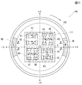
図11は角度検出センサ100の構成を示す平面図であり、角度検出センサ100は前記回転中心Oに対して回転するホイール102とその内部にパッケージ101とが設けられている。
FIG. 11 is a plan view showing the configuration of the
前記パッケージ101内には前記回転中心Oに対して対称の位置(回転中心Oの回りに互いに90°ずれた位置)に4つのチップ基板(ウェハ)K1,K2,K3,K4がそれぞれ設けられている。一つのチップ基板には、交換バイアス層(反強磁性体層)と、固定層(ピン止め層)と、非磁性層と、自由層(フリー磁性層)とが積層された構造を基本とする磁気抵抗効果素子としてのGMR素子(個別にG1ないしG8で示す)が2ヶづつ設けられている。
In the
すなわち、前記チップ基板K1にはGMR素子G1とG2が設けられ、チップ基板K2にはGMR素子G3とG4が設けられ、チップ基板K3にはGMR素子G5とG6が設けられ、チップ基板K4にはGMR素子G7とG8が設けられている。各チップ基板K1〜K4に搭載された各GMR素子G1〜G8は、GMR素子G1とGMR素子G4とが直列接続され且つGMR素子G3とGMR素子G2とが直列接続された状態で両者が並列に接続されて第1のブリッジ回路が構成されている。同様にGMR素子G5とGMR素子G8とが直列接続され且つGMR素子G7とGMR素子G6とが直列接続された状態で両者が並列に接続されて第2のブリッジ回路が構成されている(図1参照)。 That is, the chip substrate K1 is provided with GMR elements G1 and G2, the chip substrate K2 is provided with GMR elements G3 and G4, the chip substrate K3 is provided with GMR elements G5 and G6, and the chip substrate K4 is provided with GMR elements G7 and G8 are provided. The GMR elements G1 to G8 mounted on the chip substrates K1 to K4 are parallel to each other with the GMR element G1 and the GMR element G4 being connected in series and the GMR element G3 and the GMR element G2 being connected in series. A first bridge circuit is configured by connection. Similarly, the GMR element G5 and the GMR element G8 are connected in series, and the GMR element G7 and the GMR element G6 are connected in series to form a second bridge circuit (FIG. 1). reference).
磁石M1,M2は前記ホイール102の内面に固着されている。一方の磁石M1はN極が回転中心Oに向けられ且つ他方の磁石M2はS極が回転中心Oに向けられた状態で固着されており、前記磁石M1と磁石M2の間には一定の外部磁界Hが発生している。
Magnets M1 and M2 are fixed to the inner surface of the
被測定物である回転部材が回転して前記ホイール102が回転させられると、前記磁石M1,M2がパッケージ101の回りを周回する。このとき、前記外部磁界Hに応じて各GMR素子G1〜G8の自由層の磁化の向きが変化させられる。これにより前記各GMR素子G1〜G8の抵抗値が、前記自由層の磁化の向きと前記固定層の磁化の向きとのなす角に応じて変化するため、前記第1のブリッジ回路から+sin信号と−sin信号が出力され、同時に前記第2のブリッジ回路からは第1のブリッジ回路の±sin信号から位相が90°ずれた+cos信号と−cos信号が出力される。
When the rotating member as the object to be measured rotates and the
制御部は、これら4つの信号のうち、前記+sin信号と−sin信号とを差動増幅してSIN信号(正弦波信号)を生成し、且つ前記+cos信号と−cos信号とを差動増幅してCOS信号(余弦波信号)を生成する。次に、前記制御部は前記SIN信号(正弦波信号)とCOS信号(余弦波信号)とから正接値(tan)を計算し、さらに逆正接値(arctan)を求めることにより、前記回転部材の出力角度を検出することが可能となっている。
前記角度検出センサ100では、回転部材の回転角を高精度に検出するためには、前記正弦波信号と余弦波信号との間の位相差90°を高精度に保つことが必要である。そして、そのためには同一のチップ基板に設けられた2ヶのGMR素子の前記固定層の磁化方向(磁化の向き)eは同一方向で製造されるものであるから、例えばチップ基板K1の磁化方向eを+Y方向とすると、チップ基板K2の磁化方向eは−Y方向、チップ基板K3の磁化方向eは+X方向、チップ基板K4の磁化方向eは−X方向、というように隣り合うチップ基板間で前記磁化方向eが互いに高い精度の90°間隔でずれるように実装する必要がある。
In the
しかし、GMR素子G1〜G8の固定層の磁化方向eは目視によって確認することが不可能であるため、前記磁化方向eが正確に90°ずれるように各チップ基板K1〜K4をパッケージ上に実装することは困難であり、前記90°を正確に設定することができない場合には、位相誤差αが90°±αとして発生し前記回転部材の回転角(出力角度)を高精度に検出できなくなるという問題があった。 However, since the magnetization direction e of the fixed layers of the GMR elements G1 to G8 cannot be visually confirmed, the chip substrates K1 to K4 are mounted on the package so that the magnetization direction e is accurately shifted by 90 °. When the 90 ° cannot be set accurately, the phase error α occurs as 90 ° ± α, and the rotation angle (output angle) of the rotating member cannot be detected with high accuracy. There was a problem.
また各チップ基板が高い精度で切り出されており、且つGMR素子G1〜G8の磁化方向eがチップ基板の一辺に対して高い精度で平行に形成されている場合には、例えば画像認識装置などの実装角度を補正する装置を駆使してパッケージ上にチップ基板どうしを90°に実装することにより前記磁化方向eを正確に90°ずらすことが可能であるが、この場合には前記チップ基板の製造コストが高騰しやすく、また実装時の組み立て工手が複雑になって組み立て時間や組み立てコストが増大するという問題がある。 Further, when each chip substrate is cut out with high accuracy and the magnetization direction e of the GMR elements G1 to G8 is formed with high accuracy parallel to one side of the chip substrate, for example, an image recognition device or the like By making full use of a device for correcting the mounting angle and mounting the chip substrates at 90 ° on the package, the magnetization direction e can be accurately shifted by 90 °. In this case, the manufacture of the chip substrate is possible. There is a problem that the cost is likely to rise, and the assembling process at the time of mounting becomes complicated, resulting in an increase in assembling time and assembling cost.
一方、上記角度検出センサ100では、出力角度φが、前記ホイール102が回転する入力角度(磁石回転角度)θに正確に比例して出力されることが理想的であるが、実際の出力角度φは一次関数で変化する直線上に正弦波状の信号が重畳した歪み誤差が現れるものとなり、前記出力角度φが前記入力角度θに正確に比例しないことがある(図6参照)。
On the other hand, in the
このような歪み誤差が発生する原因は、前記GMR素子特有の抵抗値歪みに起因することが知られており、前記角度検出センサ100の出力である前記4つの信号波形に各々このような歪み誤差が生じると、前記SIN信号およびCOS信号にも歪み誤差が発生し、ひいては前記正接値(tan)や逆正接値(arctan)の計算においても前記歪み誤差の影響を受けるため、角度検出センサから検出される出力角度φの精度を高めることができないという問題があった。
It is known that the cause of such a distortion error is caused by a resistance value distortion peculiar to the GMR element, and each of the four signal waveforms as the output of the
前記位相誤差αや歪み誤差βは所定の関数で近似することができ、その近似関数を用いて前記角度検出センサ100のから出力される出力角度φを角度ごとに補償することができれば、前記出力角度φの精度を大幅に高めることが可能である。しかし、所定の関数を構成する補正係数を容易に算出することができず、上記特許文献1、2、3および4にも補正係数を得る方法に関する記載は存在しない。
The phase error α and the distortion error β can be approximated by a predetermined function, and if the output angle φ output from the
本発明は上記従来の課題を解決するためのものであり、磁気抵抗効果素子から出力される4つの信号に、上記のような位相誤差および/または歪み誤差による誤差信号が含まれているような場合にも、これらの影響を少なくして検出される出力角度の検出精度を高めることを可能とした補償機能を備えた角度検出センサを提供することを目的としている。 The present invention is to solve the above-described conventional problems, and the four signals output from the magnetoresistive effect element include an error signal due to the phase error and / or distortion error as described above. Even in this case, an object of the present invention is to provide an angle detection sensor having a compensation function that can improve the detection accuracy of the output angle detected by reducing these effects.
また本発明は位相誤差αや歪み誤差βを近似的に示す位相補償値および歪み補償値を容易に算出することが可能な補償機能を備えた角度検出センサを提供することを目的としている。 It is another object of the present invention to provide an angle detection sensor having a compensation function that can easily calculate a phase compensation value and a distortion compensation value that approximately indicate a phase error α and a distortion error β.
本発明は、被測定物に与えられた回転に応じて回転磁界を発生するとともに前記回転磁界を感知して前記回転の入力角度に応じた複数の出力信号を出力するセンサ部と、前記出力信号から前記被測定物が回転した角度を出力角度として算出する信号処理部と、を備えた角度検出センサにおいて、
前記信号処理部には、前記出力信号から所定の位相差を有する2種類の信号を生成する信号変換手段と、前記2種類の信号から前記被測定物の補償前における出力角度を算出する第1の関数演算手段と、前記補償前の出力角度に含まれている誤差信号を除去する補償値を算出する補償手段と、前記補償手段が前記補償値を算出するときに用いる補償係数を予め取得して記憶しておくメモリ手段と、前記メモリ手段の記憶されている補償係数を読み出して前記補償手段に与える制御部と、が設けられ、
前記誤差信号が、前記センサ部が有する特性に基づいて発生する歪み誤差であり、前記補償手段には前記歪み誤差を減少させる歪み補償値を生成する歪み補償部が設けられていることを特徴とするものである。
The present invention provides a sensor unit that generates a rotating magnetic field according to rotation given to an object to be measured and senses the rotating magnetic field and outputs a plurality of output signals according to an input angle of the rotation, and the output signal In an angle detection sensor comprising: a signal processing unit that calculates an output angle as an angle at which the object to be measured is rotated from
The signal processing unit includes a signal conversion unit that generates two types of signals having a predetermined phase difference from the output signal, and a first that calculates an output angle of the device under test before compensation from the two types of signals. Function calculating means, a compensation means for calculating a compensation value for removing an error signal included in the output angle before compensation, and a compensation coefficient used when the compensation means calculates the compensation value. a memory means for storing Te, wherein a control unit that reads the compensation coefficient stored in the memory means given to the compensating means, is provided, et al is,
The error signal is a distortion error generated based on characteristics of the sensor unit, and the compensation unit is provided with a distortion compensation unit that generates a distortion compensation value for reducing the distortion error. To do.
また本発明は、被測定物に与えられた回転に応じて回転磁界を発生するとともに前記回転磁界を感知して前記回転の入力角度に応じた複数の出力信号を出力するセンサ部と、前記出力信号から前記被測定物が回転した角度を出力角度として算出する信号処理部と、を備えた角度検出センサにおいて、
前記信号処理部には、前記出力信号から所定の位相差を有する2種類の信号を生成する信号変換手段と、前記2種類の信号から前記被測定物の補償前における出力角度を算出する第1の関数演算手段と、前記補償前の出力角度に含まれている誤差信号を除去する補償値を算出する補償手段と、前記補償手段が前記補償値を算出するときに用いる補償係数を予め取得して記憶しておくメモリ手段と、前記メモリ手段の記憶されている補償係数を読み出して前記補償手段に与える制御部と、が設けられ、
前記誤差信号が、前記2種類の信号間に存在する前記所定の位相差を超えたことによって発生する位相誤差および前記センサ部が有する特性に基づいて発生する歪み誤差であり、前記補償手段には前記位相誤差を減少させる位相補償値を生成する位相補償部および前記歪み誤差を減少させる歪み補償値を生成する歪み補償部が設けられているものである。
According to another aspect of the present invention, there is provided a sensor unit that generates a rotating magnetic field according to the rotation given to the object to be measured, senses the rotating magnetic field, and outputs a plurality of output signals according to the rotation input angle; In an angle detection sensor comprising: a signal processing unit that calculates, as an output angle, an angle at which the measured object rotates from a signal,
The signal processing unit includes a signal conversion unit that generates two types of signals having a predetermined phase difference from the output signal, and a first that calculates an output angle of the device under test before compensation from the two types of signals. Function calculating means, a compensation means for calculating a compensation value for removing an error signal included in the output angle before compensation, and a compensation coefficient used when the compensation means calculates the compensation value. A memory means for storing and a controller for reading the compensation coefficient stored in the memory means and providing the compensation means to the compensation means,
The error signal is a phase error generated due to exceeding the predetermined phase difference existing between the two types of signals and a distortion error generated based on the characteristics of the sensor unit. in which the distortion compensation unit for generating a distortion compensation value for reducing the phase compensating portion and the distortion error for generating a phase compensation value for reducing the phase error is eclipsed set.
上記において、前記メモリ手段には、前記補償前の出力角度に含まれる誤差信号をサンプリングして取得したデータに対し離散フーリエ変換を行って得られる値が補償係数として記憶されているものが好ましい。 In the above, it is preferable that the memory means stores a value obtained by performing a discrete Fourier transform on data obtained by sampling an error signal included in the output angle before compensation as a compensation coefficient.
上記において、前記補償係数が、位相補償係数と歪み補償係数の少なくとも一方である。
この場合、前記位相補償係数に与えられる正負の符号が、前記離散フーリエ変換を行って得られた高調波を複素数で表したときの実数の符号により決定することができる。
In the above, the compensation coefficient is at least one of a phase compensation coefficient and a distortion compensation coefficient.
In this case, the positive or negative sign given to the phase compensation coefficient can be determined by a real sign when the harmonics obtained by performing the discrete Fourier transform are represented by complex numbers.
例えば、前記位相補償係数が2次高調波成分から得られるものとすることができ、前記歪み補償係数が4次高調波成分から得られるものとすることができる。 For example, the phase compensation coefficient can be obtained from a second harmonic component, and the distortion compensation coefficient can be obtained from a fourth harmonic component .
本発明では、角度検出センサの出力角度の精度を高める位相補償値と歪み補正値とを容易に求めることができる。 In the present invention, it is possible to easily obtain a phase compensation value and a distortion correction value that enhance the accuracy of the output angle of the angle detection sensor.
しかも、位相補償係数とその符号、および歪み補償係数を記憶しておくだけでよいため、データ量が少なく、その読み出し時間も大幅に短縮することが可能である。よって、角度検出センサの出力角度をリアルタイムで検出することが可能となる。 Moreover, since it is only necessary to store the phase compensation coefficient, its sign, and the distortion compensation coefficient, the amount of data is small, and the readout time can be greatly shortened. Therefore, the output angle of the angle detection sensor can be detected in real time.
図1は本発明の角度検出センサの構成を示すブロック構成図、図2は2組のブリッジ回路から出力される4つの信号の関係を理想的な場合として示す波形図である。以下に説明する角度検出センサは、自動車のステアリングシャフトなどの回転部材の出力角度を検出するものである。 FIG. 1 is a block diagram showing the configuration of the angle detection sensor of the present invention, and FIG. 2 is a waveform diagram showing the relationship between four signals output from two sets of bridge circuits as an ideal case. An angle detection sensor described below detects an output angle of a rotating member such as a steering shaft of an automobile.
図1に示す角度検出センサは、センサ部1と前記センサ部1から出力される出力信号の処理を行う信号処理部10を有している。なお、図示P−P線より左側がセンサ部1を示し、右側が信号処理部10を示している。
The angle detection sensor shown in FIG. 1 includes a
前記センサ部1の構成は上記「背景技術」の欄において説明したものと同様である。すなわち、図11に示すように前記センサ部1は回転中心Oに対して回転自在に設けられたホイール102と、前記ホイール102の内部に4つのチップ基板(ウェハ)K1,K2,K3およびK4を搭載したパッケージ103とを有している。前記4つのチップ基板K1〜K4は、前記パッケージ103内において前記回転中心Oに対して対称の位置、すなわち回転中心Oの回りに互いに90°間隔でずれた位置にそれぞれ設けられている。
The configuration of the
一つのチップ基板には、交換バイアス層(反強磁性体層)と、固定層(ピン止め層)と、非磁性層と、自由層(フリー磁性層)とが積層された構造(図示せず)を基本とする磁気抵抗効果素子としてのGMR素子(個別にG1ないしG8で示す)が2ヶづつ設けられている。 One chip substrate has a structure in which an exchange bias layer (antiferromagnetic layer), a fixed layer (pinned layer), a nonmagnetic layer, and a free layer (free magnetic layer) are stacked (not shown). Two GMR elements (indicated individually as G1 to G8) are provided as magnetoresistive effect elements.
前記チップ基板は、一つの大型の基板上に複数のGMR素子が成膜された状態で外部磁場を掛け、前記固定層の磁化の向き(磁化方向)が一定の方向に揃えられた後に個々のチップ基板K1〜K4に切り分けられるため、1つのチップ基板上に設けられた2つのGMR素子の固定層の磁化方向は同一である。そして、各チップ基板K1〜K4は前記磁化方向が隣り合う基板間でほぼ90°の関係を有すように、前記パッケージ101内に固定されている。なお、前記90°の関係は正確な方が好ましいが、後述する位相補償回路により必ずしも高精度に90°の関係である必要はない。
The chip substrate is subjected to an external magnetic field in a state where a plurality of GMR elements are formed on a single large substrate, and the magnetization direction (magnetization direction) of the fixed layer is aligned in a certain direction. Since it is divided into chip substrates K1 to K4, the magnetization directions of the fixed layers of the two GMR elements provided on one chip substrate are the same. The chip substrates K1 to K4 are fixed in the
前記チップ基板K1〜K4に搭載された各GMR素子G1〜G8は、第1のブリッジ回路WB1と第2のブリッジ回路WB2とを構成している。図1に示すように、第1のブリッジ回路WB1は前記回転中心Oに対して軸対称に設けられたチップ基板K1とチップ基板K2に搭載されたGMR素子G1,G2およびG3,G4で構成されている。すなわち、第1のブリッジ回路WB1は前記GMR素子G1とGMR素子G4とを直列に接続した回路と、前記GMR素子G3とGMR素子G2とを直列に接続した回路とが、並列に接続されて形成されている。同様に第2のブリッジ回路WB2は前記回転中心Oに対して軸対称に設けられたチップ基板K3とチップ基板K4に搭載されたGMR素子G5,G6およびG7,G8で構成されている。第2のブリッジ回路WB2は前記GMR素子G5とGMR素子G8とを直列に接続した回路と、前記GMR素子G7とGMR素子G6とを直列に接続した回路とが、並列に接続されて形成されている。 The GMR elements G1 to G8 mounted on the chip substrates K1 to K4 constitute a first bridge circuit WB1 and a second bridge circuit WB2. As shown in FIG. 1, the first bridge circuit WB1 is composed of chip substrates K1 and GMR elements G1, G2 and G3, G4 mounted on the chip substrate K2 and arranged symmetrically with respect to the rotation center O. ing. That is, the first bridge circuit WB1 is formed by connecting a circuit in which the GMR element G1 and the GMR element G4 are connected in series and a circuit in which the GMR element G3 and the GMR element G2 are connected in series. Has been. Similarly, the second bridge circuit WB2 is composed of a chip substrate K3 provided symmetrically with respect to the rotation center O and GMR elements G5, G6 and G7, G8 mounted on the chip substrate K4. The second bridge circuit WB2 is formed by connecting a circuit in which the GMR element G5 and the GMR element G8 are connected in series and a circuit in which the GMR element G7 and the GMR element G6 are connected in series to each other. Yes.
そして、前記並列に接続された第1のブリッジ回路WB1と第2のブリッジ回路WB2の一方の端部が電源Vccに接続され、他方の端部がグランドGNDに接地されている。 One end of the first bridge circuit WB1 and the second bridge circuit WB2 connected in parallel is connected to the power source Vcc, and the other end is grounded to the ground GND.
前記ホイール102と被測定物である回転部材(ステアリングシャフトなど)とは例えばギヤなどを介して連結されており、回転部材の回転に応じて前記ホイール102が回転されられるように構成されている。よって、前記回転部材を回転させると、前記ホイール102が回転させられるため、前記磁石M1,M2が前記パッケージ101の周囲を周回できるようになっている。
The
このとき前記磁石M1,M2間に発生している外部磁場Hが、前記パッケージ101内の各GMR素子G1〜G8に対して回転磁界を与えるため、各GMR素子G1〜G8を形成する自由層の磁化の向きが変化させられる。これにより前記各GMR素子G1〜G8の抵抗値が、前記自由層の磁化の向きと前記固定層の磁化の向きとのなす角に応じて変化する。よって、前記第1のブリッジ回路WB1を構成するGMR素子G3とGMR素子G2との接続部と、GMR素子G1とGMR素子G4との接続部とから互いの位相が180°異なる正弦波状の2つの信号が出力される。同時に前記第2のブリッジ回路WB2を構成するGMR素子G7とGMR素子G6との接続部と、GMR素子G5とGMR素子G8との接続部とからも互いの位相が180°異なる正弦波状の2つの信号が出力される。
At this time, the external magnetic field H generated between the magnets M1 and M2 gives a rotating magnetic field to the GMR elements G1 to G8 in the
ただし、回転中心Oに軸対称に配置されたチップ基板K1,K2と同じく回転中心に軸対称に配置されたチップ基板K3,K4とは、さらに前記回転中心Oに対しほぼ90°異なる位置に配置されているため、前記第1のブリッジ回路WB1から出力される2つの信号を+sin信号,−sin信号とすると、前記第2のブリッジ回路WB2から出力される2つの信号は+cos信号,−cos信号となる(図2参照)。 However, the chip substrates K1 and K2, which are arranged symmetrically with respect to the rotation center O, and the chip substrates K3 and K4 which are arranged symmetrically with respect to the rotation center are arranged at positions that are approximately 90 ° different from the rotation center O. Therefore, if the two signals output from the first bridge circuit WB1 are the + sin signal and the −sin signal, the two signals output from the second bridge circuit WB2 are the + cos signal and the −cos signal. (See FIG. 2).
この実施の形態に示すように、例えば前記ホイール102が時計回り方向に回転したときに前記第1のブリッジ回路WB1のGMR素子G3とGMR素子G2の接続部から出力される正弦波状の信号を+sin信号とすると、前記GMR素子G1とGMR素子G4の接続部からは−sin信号が出力されることになる。このとき前記第2のブリッジ回路WB2の前記GMR素子G7とGMR素子G6の接続部からは+cos信号が出力され、前記GMR素子G5とGMR素子G8の接続部からは−cos信号が出力されることになる。
As shown in this embodiment, for example, when the
信号処理部10は、主として制御手段11、第1の信号変換手段12Aおよび第2の信号変換手段12B、信号調整手段13、第1の関数演算手段14、メモリ手段15、補償手段20などを有している。
The
前記制御手段11はCPUを主体に構成され、前記信号調整手段13、第1の関数演算手段14および補償手段20などにおける一連の信号処理を統括する機能を有している。前記第1,第2の信号変換手段12A,12Bは差動増幅手段12a,12aおよびA/D変換手段12b,12bを有している。前記第1の信号変換手段12Aの差動増幅手段12aは、前記第1のブリッジ回路WB1から出力される前記2種類の+sin信号と−sin信号とを差動増幅して2倍の振幅からなるsin信号を生成するとともに、前記A/D変換手段12bが増幅後の信号を所定のサンプリング周期でA/D変換したSIN信号(デジタル信号)に変換する。同様に前記第2の信号変換手段12Bの差動増幅手段12aは、前記第2のブリッジ回路WB2から出力される前記2種類の+cos信号と−cos信号とを差動増幅して2倍の振幅からなるcos信号を生成するとともに、前記A/D変換手段12bが増幅後の信号をA/D変換したCOS信号(デジタル信号)に変換する。
The control means 11 is mainly composed of a CPU, and has a function of supervising a series of signal processing in the signal adjustment means 13, the first function calculation means 14, the compensation means 20, and the like. The first and second signal conversion means 12A and 12B have differential amplification means 12a and 12a and A / D conversion means 12b and 12b. The
ここで、例えばA1,A2,B1およびB2を振幅係数、a1,a2,b1およびb2をオフセット係数とし、前記+sin信号を+A1・sinθ+a1、前記−sin信号を−A2・sinθ−a2、前記+cos信号を+B1・cosθ+b1、前記−cos信号を−B2・cosθ−b2で表すと、前記第1の信号変換手段12Aで生成される前記SIN信号は、(+A1・sinθ+a1)−(−A2・sinθ−a2)=(A1+A2)・sinθ+(a1+a2)となる。同様に前記第2の信号変換手段12Bで生成されるCOS信号は、(+B1・cosθ+b1)−(−B2・cosθ−b2)=(B1+B2)・cosθ+(b1+b2)となる。 Here, for example, A1, A2, B1 and B2 are amplitude coefficients, a1, a2, b1 and b2 are offset coefficients, the + sin signal is + A1 · sin θ + a1, the −sin signal is −A2 · sin θ−a2, and the + cos signal. Is expressed as + B1 · cos θ + b1 and the −cos signal is expressed as −B2 · cos θ−b2, the SIN signal generated by the first signal converting means 12A is (+ A1 · sin θ + a1) − (− A2 · sin θ−a2). ) = (A1 + A2) · sin θ + (a1 + a2). Similarly, the COS signal generated by the second signal converting means 12B is (+ B1 · cos θ + b1) − (− B2 · cos θ−b2) = (B1 + B2) · cos θ + (b1 + b2).
前記信号調整手段13は、前記SIN信号とCOS信号のオフセット調整や利得調整を行い、両信号の振幅方向の基準(0点)と量(振幅量)とを一致させる機能を有している。すなわち、上記の例でいえば、利得調整とはA1+A2=B1+B2とすることにより、前記SIN信号とCOS信号の振幅係数を同じ値にすることを意味し、オフセット調整とはa1+a2=b1+b2=0として振幅の基準が原点位置(0点)に一致するようにしてバイアス電圧が重畳することによるずれを無くすことを意味している。よって、この時点におけるSIN信号は(A1+A2)・sinθとなり、COS信号は(B1+B2)・cosθとなっている(ただし、A1+A2=B1+B2)。 The signal adjusting means 13 has a function of performing offset adjustment and gain adjustment of the SIN signal and the COS signal, and matching the reference (0 point) and amount (amplitude amount) of the amplitude direction of both signals. That is, in the above example, the gain adjustment means that the amplitude coefficient of the SIN signal and the COS signal is set to the same value by setting A1 + A2 = B1 + B2, and the offset adjustment means that a1 + a2 = b1 + b2 = 0. This means that the deviation due to the bias voltage being superposed is eliminated so that the amplitude reference coincides with the origin position (0 point). Therefore, the SIN signal at this time is (A1 + A2) · sin θ, and the COS signal is (B1 + B2) · cos θ (where A1 + A2 = B1 + B2).
前記第1の関数演算手段14は、sin,cos,tan,tan−1=arctan,sinh,cosh,exp,logなどの関数値の計算を行うソフトウェア、例えば周知のCORDIC(Coordinate Rotation Digital Computer)アルゴリズムを用いた数値計算ソフトウェアを搭載しており、ここでは前記SIN信号を前記COS信号で除することにより正接値(tan=SIN信号/COS信号=sinθ/cosθ)を計算するTAN処理と、前記TAN処理で求めた値から逆正接値(arctan(sinθ/cosθ))を計算して被測定物の補償前の出力角度φ[°]を求めるATAN処理とを有している。 The first function calculation means 14 is software for calculating function values such as sin, cos, tan, tan −1 = arctan, sinh, cosh, exp, log, for example, a well-known CORDIC (Coordinate Rotation Digital Computer) algorithm. TAN processing for calculating a tangent value (tan = SIN signal / COS signal = sin θ / cos θ) by dividing the SIN signal by the COS signal, and the TAN And Atan processing for calculating the arc tangent value (arctan (sin θ / cos θ)) from the value obtained by the processing to obtain the output angle φ [°] before compensation of the object to be measured.
この実施の形態における補償手段20は位相補償部20A、歪み補償部20B、加算手段27、減算手段28などを有している。前記位相補償部20Aは、第1の倍角手段21と、第2の関数演算手段22と、位相補償値生成手段23とで構成されている。また前記歪み補償部20Bは第2の倍角手段24と、第3の関数演算手段25と、歪み補償値生成手段26とで構成されている。なお、前記第2の関数演算手段22と第3の関数演算手段25とは、上記前記第1の関数演算手段14同様のCORDICアルゴリズムを用いた関数演算手段で構成されている。
The
第1の倍角手段21は前記第1の関数演算手段14のATAN処理により求めた補償前の出力角度φを2倍化(2φ)して出力する機能を有している。また第2の倍角手段24は、前記第1の倍角手段21が2倍化した補償前の出力角度2φを、さらに2倍化(合計4倍化(4φ))して出力する機能を有している。なお、前記第1,第2の倍角手段21,24は例えばシフトレジスタなどで構成されており、2進法で表記される前記補償前の出力角度φに相当するデータを左に1ビットシフトすることにより2φ(2倍化)することができ、さらに1ビット左にシフトすることにより容易に4φ(4倍化)することが可能とされている。 The first double angle means 21 has a function of doubling (2φ) the output angle φ before compensation obtained by the ATRAN processing of the first function calculation means 14 and outputting it. Further, the second double angle means 24 has a function of further doubling the output angle 2φ before compensation (doubled in total (4φ)) output by the first double angle means 21 by double. ing. The first and second double angle means 21 and 24 are composed of shift registers, for example, and shift data corresponding to the output angle φ before compensation expressed in binary notation to the left by 1 bit. Thus, 2φ (doubled) can be obtained, and further 4φ (fourfold) can be easily achieved by shifting left by 1 bit.
前記第2の関数演算手段22では、CORDICアルゴリズムを用いて前記第1の倍角手段21から出力された信号2φからcos(2φ)を生成し出力する。同様に、前記第3の関数演算手段25は、CORDICアルゴリズムを用いて前記第2の倍角手段24から出力された信号4φからsin(4φ)を生成し出力する。 The second function calculating means 22 generates and outputs cos (2φ) from the signal 2φ output from the first double angle means 21 using the CORDIC algorithm. Similarly, the third function calculation means 25 generates sin (4φ) from the signal 4φ output from the second double angle means 24 using the CORDIC algorithm and outputs it.
なお、前記第1の関数演算手段14、第2の関数演算手段22および第3の関数演算手段25とが一つの関数演算手段を共有する構成であり、上記の各計算が前記関数演算手段を用いて前記制御手段11の制御に基づいて行われる構成であってもよい。
The first
前記位相補償値生成手段23は、第2の関数演算手段22から出力される前記cos(2φ)と前記メモリ手段15に記憶されている位相補償係数α0およびその符号を読み出して位相補償値(Δφα)compを生成する。また前記歪み補償値生成手段26は、第3の関数演算手段25から出力される前記sin(4φ)と前記メモリ手段15に記憶されている歪み補償係数β0を読み出して歪み補償値(Δφβ)compを生成する。 The phase compensation value generation means 23 reads out the cos (2φ) output from the second function calculation means 22, the phase compensation coefficient α 0 and the sign stored in the memory means 15, and reads out the phase compensation value ( Δφ α ) Comp is generated. The distortion compensation value generation means 26 reads out the sin (4φ) output from the third function calculation means 25 and the distortion compensation coefficient β 0 stored in the memory means 15 to read out the distortion compensation value (Δφ β ) Generate comp .
なお、前記位相補償値(Δφα)compおよび歪み補償値(Δφβ)compを得る具体的な方法については後述する。 A specific method for obtaining the phase compensation value (Δφ α ) comp and the distortion compensation value (Δφ β ) comp will be described later.
前記加算手段27は位相補償値(Δφα)compと歪み補償値(Δφβ)compを加算して減算手段28に与える。そして、前記減算手段28は、前記第1の関数演算手段14のATAN処理で求めた補償前の出力角度φから前記位相補償値(Δφα)compと歪み補償値(Δφβ)compを減算することにより、精度の高い出力角度φOUTを出力する機能を有している。なお、前記加算手段27と減算手段28に代わるその他の構成としては、前記補償前の出力角度φから最初に前記位相補償値(Δφα)compと歪み補償値(Δφβ)compの一方を減算し、次に他方を減算するものであってもよい。 The adding means 27 adds the phase compensation value (Δφ α ) comp and the distortion compensation value (Δφ β ) comp to give to the subtracting means 28. Then, the subtracting means 28 subtracts the phase compensation value (Δφ α ) comp and the distortion compensation value (Δφ β ) comp from the pre-compensation output angle φ obtained by the ATRAN processing of the first function computing means 14. Thus, it has a function of outputting a highly accurate output angle φ OUT . As another configuration replacing the adding means 27 and the subtracting means 28, one of the phase compensation value (Δφ α ) comp and the distortion compensation value (Δφ β ) comp is first subtracted from the output angle φ before the compensation. Then, the other may be subtracted.
これにより前記SIN信号とCOS信号との間の位相誤差αを無くして両者の関係を高精度で90°に保つことができ、同時に前記補償前の出力角度φに含まれる抵抗値歪に基づく歪み誤差βを取り除くことができ、精度の高い出力角度φOUTを得るこができる。 As a result, the phase error α between the SIN signal and the COS signal can be eliminated, and the relationship between the two can be maintained at 90 ° with high accuracy, and at the same time, distortion based on resistance value distortion included in the output angle φ before compensation. The error β can be removed, and a highly accurate output angle φ OUT can be obtained.
次に、前記位相補償値(Δφα)compを得る具体的な方法について説明する。
図3はブリッジ回路の出力であるSIN信号とCOS信号との間に位相誤差を含む場合を示す波形図である。
Next, a specific method for obtaining the phase compensation value (Δφ α ) comp will be described.
FIG. 3 is a waveform diagram showing a case where a phase error is included between the SIN signal and the COS signal which are the outputs of the bridge circuit.
チップ基板K1〜K4に設けられたGMR素子G1ないしG8を構成する前記固定層の磁化方向が隣り合う基板間において90°の関係が維持されない場合には、前記第1,第2の信号変換手段12A,12Bからそれぞれ出力されるSIN信号とCOS信号とは元々の位相差(90°)からずれている。 If the 90 ° relationship between the adjacent magnetization directions of the fixed layers constituting the GMR elements G1 to G8 provided on the chip substrates K1 to K4 is not maintained, the first and second signal conversion means The SIN signal and COS signal output from 12A and 12B, respectively, deviate from the original phase difference (90 °).
前記ホイール102の出力角度、すなわち前記角度検出センサ100に入力される入力角度をθ、このときの位相誤差(位相差90°からのずれ量)をα度とし、且つ前記第2のブリッジ回路WB2から出力される+cos信号を+cosθ、−cos信号を−cosθとする。なお、ここでは説明の都合上、前記振幅係数A1,A2,B1およびB2をA1=A2=B1=B2=1、前記オフセット係数a1,a2,b1およびb2をa1=a2=b1=b2=0としている。このようにしても、結局は前記信号調整手段13やTAN処理によって同様の効果、すなわち前記各係数が消去されてしまうため、特に問題はない。
The output angle of the
前記第2のブリッジ回路WB2から出力される+cosθと−cosθを基準とすると、前記第1のブリッジ回路WB1から出力される+sin信号は+sin(θ+α)、−sin信号は−sin(θ+α)と表すことができる。よって、前記第1の信号変換手段12Aから出力されるSIN信号は+sin(θ+α)−(−sin(θ+α))=2sin(θ+α)となり、前記第2の信号変換手段12Bから出力されるCOS信号は+cosθ−(−cosθ)=2cosθとなり、これを図示すると図3のように表される。なお、図3以下においては、前記位相誤差αの例としてα=+5度とした場合を示している。
Based on + cos θ and −cos θ output from the second bridge circuit WB2, the + sin signal output from the first bridge circuit WB1 is expressed as + sin (θ + α), and the −sin signal is expressed as −sin (θ + α). be able to. Therefore, the SIN signal output from the first
前記第1,第2の信号変換手段12A,12Bから出力された前記SIN信号とCOS信号は前記信号調整手段13においてオフセット調整と利得調整とが行われる。次に、前記第1の関数演算手段14のTAN処理によって正接値(tan=SIN信号/COS信号)が2sin(θ+α)/2cosθ=sin(θ+α)/cosθとして計算される。さらにATAN処理によって逆正接値(arctan)が計算されるが、位相誤差αが生じている場合の前記第1の関数演算手段14の出力である被測定物の補償前の出力角度をφαとすると、φα=arctan(sin(θ+α)/cosθ))である。
The SIN signal and COS signal output from the first and second signal conversion means 12A and 12B are subjected to offset adjustment and gain adjustment in the signal adjustment means 13. Next, the tangent value (tan = SIN signal / COS signal) is calculated as 2 sin (θ + α) / 2 cos θ = sin (θ + α) / cos θ by the TAN processing of the first function calculating means 14. Although arctangent (arctan) are calculated by addition ATAN processing, and the output angle before compensation of the object to be measured which is the output of the first
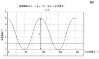
図4は位相誤差を含む場合において、ATAN処理後の補償前の出力角度φαを連続的な関数として示す波形図、図5は補償前の出力角度φαと入力角度θとの差を検出位相誤差Δφα(=φα−θ)として示す波形図である。 FIG. 4 is a waveform diagram showing the output angle φ α before compensation after the Atan processing as a continuous function when phase error is included, and FIG. 5 detects the difference between the output angle φ α before compensation and the input angle θ. It is a waveform diagram shown as a phase error Δφ α (= φ α −θ).
図4では、入力角度θと補償前の出力角度φαが一対一で対応している。しかし、ATAN処理後の補償前の出力角度φαは理想的な出力角度である一次直線(φ=θ)に三角関数が重畳した形となっている。 In FIG. 4, there is a one-to-one correspondence between the input angle θ and the output angle φ α before compensation. However, the output angle φ α before compensation after the ATAAN processing has a form in which a trigonometric function is superimposed on a linear line (φ = θ) that is an ideal output angle.
ここで前記補償前の出力角度φαから入力角度θを差し引くことにより検出される位相の差(φα−θ)を検出位相誤差Δφαとして求めてみると、入力角度θと検出位相誤差Δφα(=φα−θ)との関係は図5に示すような正弦波状の周期関数(三角関数)として表される。なお、前記検出位相誤差Δφαは、最初に与えておいた位相誤差αに基づいて発生したものであり、つまりはチップ基板K1〜K4に設けられたGMR素子G1ないしG8を構成する前記固定層の磁化方向が隣り合う基板間において90°の関係が維持されないことによる影響を受けて発生したものである。 When we calculated here by the difference between the phase detected by subtracting the input angle θ from the output angle phi alpha before the compensation the (phi alpha - [theta]) as detected phase error [Delta] [phi alpha, the input angle θ and the detected phase error [Delta] [phi The relationship with α (= φ α −θ) is expressed as a sinusoidal periodic function (trigonometric function) as shown in FIG. Incidentally, the detection phase error [Delta] [phi alpha, are those generated based on the phase error alpha which had been originally given the fixed layer that is, constituting the G8 to no GMR element G1 provided in the chip substrate K1~K4 This occurs due to the influence of the 90 ° relationship not being maintained between adjacent substrates.
前記周期関数からなる検出位相誤差Δφαを分析してみると、前記4つの信号(+sin信号、−sin信号、+cos信号、−cos信号)又は前記SIN信号及びCOS信号は1周期を360°とするものである(図2及び図3参照)のに対し、前記検出位相誤差Δφαは1周期を180°とするものである(図5参照)。すなわち、前記検出位相誤差Δφαは、前記4つの信号または前記SIN信号及びCOS信号を基本信号とした場合に、この基本信号に対して2倍の周波数(1/2の周期)からなる三角関数であることがわかる。 When analyzing the detected phase error Δφ α composed of the periodic function, the four signals (+ sin signal, −sin signal, + cos signal, −cos signal) or the SIN signal and the COS signal have a period of 360 °. is intended to contrast (FIG. 2 and FIG. 3), while said detected phase error [Delta] [phi alpha is for one cycle and 180 ° (see FIG. 5). That is, the detection phase error Δφ α is a trigonometric function having a frequency (1/2 period) twice that of the basic signal when the four signals or the SIN signal and the COS signal are used as the basic signal. It can be seen that it is.
よって、検出位相誤差Δφαは以下に数1で示す三角関数で近似することが可能であり、これを位相補償値(Δφα)compと称する。
Thus, the detected phase error [Delta] [phi alpha is can be approximated by a trigonometric function indicated by the

なお、前記位相補償値(Δφα)compのピークトウピークの振幅量は前記位相誤差αに相当するが、これを位相補償係数α0と称する。 Note that the peak-to-peak amplitude amount of the phase compensation value (Δφ α ) comp corresponds to the phase error α, which is referred to as a phase compensation coefficient α 0 .
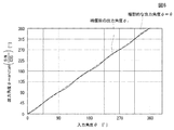
次に、抵抗値歪みに基づく歪み補償値(Δφβ)compを得る方法について説明する。
図6は抵抗値歪みに基づく歪み誤差が含まれている場合における補償前の出力角度φβを示す波形図、図7は検出歪み誤差Δφβ(=φβ−θ)を示す波形図である。なお、図7では検出歪み誤差Δφβの例として、歪み誤差βがβ=5度の場合を示している。
Next, a method for obtaining a distortion compensation value (Δφ β ) comp based on resistance value distortion will be described.
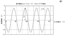
6 is a waveform diagram showing an output angle φ β before compensation when a distortion error based on resistance value distortion is included, and FIG. 7 is a waveform diagram showing a detected distortion error Δφ β (= φ β −θ). . As an example of the detection distortion error [Delta] [
前記第1のブリッジ回路WB1および第2のブリッジ回路WB2を構成する各GMR素子G1〜G8は、それぞれGMR素子特有の抵抗値歪みを有している。このため、前記第1,第2のブリッジ回路WB1,WB2から出力される前記4つの信号には前記抵抗値歪みに基づいて発生する検出歪み誤差Δφβがそれぞれ含まれている。そして、このような検出歪み誤差Δφβを含む4つの信号を用いて上記と同様の方法、すなわちTAN処理およびATAN処理を行うことにより算出した補償前の出力角度φβは、理想的な出力角度として一点鎖線で示す一次直線(φ=θ)に正弦波状の誤差信号(歪み誤差)が重畳した形として表され(図6参照)。 Each of the GMR elements G1 to G8 constituting the first bridge circuit WB1 and the second bridge circuit WB2 has a resistance value distortion peculiar to the GMR element. Therefore, the first, second bridge circuit WB1, the said four signals output from WB2 generated on the basis of the resistance value distortion detecting distortion error [Delta] [phi beta are included respectively. The output angle φ β before compensation calculated by performing the same method as described above using the four signals including the detected distortion error Δφ β , that is, the TAN process and the Atan process, is an ideal output angle. Is expressed as a form in which a sinusoidal error signal (distortion error) is superimposed on a linear line (φ = θ) indicated by a one-dot chain line (see FIG. 6).
ここで、上記位相誤差の場合同様に、前記補償前の出力角度φβから前記一次関数φ=θを減算(φβ−θ)して両者の角度ずれに相当する検出歪み誤差Δφβを求めてみると、図7に示すような正弦波状の周期関数(三角関数)として表すことができる。 As in the case of the phase error, the linear function φ = θ is subtracted from the output angle φ β before compensation (φ β −θ) to obtain a detected distortion error Δφ β corresponding to the angle deviation between the two. As a result, it can be expressed as a sinusoidal periodic function (trigonometric function) as shown in FIG.
同様に、前記周期関数である検出歪み誤差Δφβを分析してみると、1周期を360°とする基本信号(4つの信号又は前記SIN信号及びCOS信号)に対し、前記検出歪み誤差Δφβは1周期を90°とするものである(図7参照)。すなわち、前記検出歪み誤差Δφβは、前記基本信号に対して4倍の周波数(1/4の周期)からなる三角関数であることがわかる。よって、検出歪み誤差Δφβは以下に数2で示す三角関数で近似することが可能であり、これを歪み補償値(Δφβ)compと称する。
Similarly, when we analyze the a is detected distortion error [Delta] [phi beta said periodic function with respect to the fundamental signal for one period and 360 ° (4 one signal or the SIN signal and the COS signal), the detection distortion error [Delta] [phi beta Is one cycle of 90 ° (see FIG. 7). That is, the detection distortion error [Delta] [phi beta, it can be seen that with respect to the fundamental signal is a trigonometric function of four times the frequency (cycle of 1/4). Therefore, the detected distortion error Δφ β can be approximated by a trigonometric function expressed by
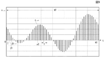
図8は総誤差信号Δφ(=Δφα+Δφβ)を示す波形図である。
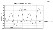
実際の角度検出センサの出力角度(補償前の出力角度)φには、上記の検出位相誤差Δφαと検出歪み誤差Δφβの2つの誤差信号が合成された状態で同時に重畳している。前記検出位相誤差Δφαと検出歪み誤差Δφβの両者を含むトータルの誤差信号を総誤差信号Δφとすると、総誤差信号Δφ(=Δφα+Δφβ)は図8に示すような1周期を180°とする周期関数からなる信号となり、このような総誤差信号Δφが理想的な出力角度として示される一次直線(φ=θ)上に重畳している。
FIG. 8 is a waveform diagram showing the total error signal Δφ (= Δφ α + Δφ β ).
The output angle (output angle before compensation) φ of the actual angle detection sensor is simultaneously superimposed on the two error signals of the detection phase error Δφ α and the detection distortion error Δφ β . Assuming that the total error signal including both the detection phase error Δφ α and the detection distortion error Δφ β is the total error signal Δφ, the total error signal Δφ (= Δφ α + Δφ β ) has a period of 180 as shown in FIG. The total error signal Δφ is superimposed on a linear line (φ = θ) shown as an ideal output angle.
したがって、第1の関数演算手段14においてATAN処理後の信号(補償前の出力角度φ)から総誤差信号Δφに相当する前記位相補償値(Δφα)compと歪み補償値(Δφβ)compを除去することができれば、精度の高い出力角度を検出することができるはずである。 Therefore, the first function calculation means 14 calculates the phase compensation value (Δφ α ) comp and the distortion compensation value (Δφ β ) comp corresponding to the total error signal Δφ from the signal after ATA processing (output angle φ before compensation). If it can be removed, it should be possible to detect a highly accurate output angle.
しかし、上記のように検出位相誤差Δφαは基本信号に対し2倍の周波数からなる上記数1の三角関数で近似できること、および検出歪み誤差Δφβは基本信号に対し4倍の周波数からなる上記数2の三角関数で近似できることまでは判明しているが、図8に示すように総誤差信号Δφを構成する検出位相誤差Δφαと検出歪み誤差Δφβとは合成された状態で存在しているため、前記総誤差信号Δφからその振幅の大きさを求めること、すなわち上記位相補償係数α0および歪み補償係数β0を求めることは困難である。つまり、前記位相誤差αに一致する位相補償係数α0および前記歪み誤差βに一致する歪み補償係数β0を見つけることができれば、前記位相補償値(Δφα)compと歪み補償値(Δφβ)compを確定することができ、精度の高い出力角度を検出することができることになる。
However, as described above, the detected phase error Δφ α can be approximated by the trigonometric function of the
そこで、以下には検出位相誤差Δφαの位相補償係数α0および検出歪み誤差Δφβの歪み補償係数β0を求める方法について説明する。 Therefore, a method for obtaining the phase compensation coefficient α 0 of the detected phase error Δφ α and the distortion compensation coefficient β 0 of the detected distortion error Δφ β will be described below.
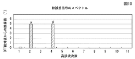
図9は総誤差信号Δφの離散周期信号を示す波形図である。
前記総誤差信号Δφの1周期分に相当する180[°]を、例えば2n(nは自然数)個のデータ数で、サンプリング周期T=180/2n[°/個]で離散的にサンプリングすることにより、離散周期信号xS(t)を得る(図9参照)。
FIG. 9 is a waveform diagram showing a discrete periodic signal of the total error signal Δφ.
For example, 180 [°] corresponding to one period of the total error signal Δφ is discretely sampled with a data number of 2 n (n is a natural number), for example, with a sampling period T = 180/2 n [° / piece]. As a result, a discrete periodic signal x S (t) is obtained (see FIG. 9).
ここで、Nを整数とすると前記離散周期信号xS(t)(総誤差信号Δφ)の1周期はNTとなり、またデルタ関数をδ(t)とすると、前記離散周期信号xS(t)は以下の数3で表すことができる。
Here, when N is an integer, one period of the discrete periodic signal x S (t) (total error signal Δφ) is NT, and when the delta function is δ (t), the discrete periodic signal x S (t) Can be expressed by the following
そして、前記離散周期信号xS(t)をフーリエ変換することにより、以下の数4に示す離散フーリエ変換式XS(f)が得られる。
Then, by performing a Fourier transform on the discrete periodic signal x S (t), a discrete Fourier transform formula X S (f) shown in the following
ここで、f=k/NTと置き換えると、離散フーリエ変換(DFT)を示す式が以下の数5として得られる。 Here, when f = k / NT is substituted, an equation indicating a discrete Fourier transform (DFT) is obtained as the following equation (5).
ただし、コンピュータなどを用いて電気的に信号処理を行うときには、サンプリング信号を有限長の長さで打ち切って計算する必要がある。サンプリングされた離散周期信号x(n)が有限長で、x(0)からx(N−1)までN個のデータを有するとき、離散フーリエ変換XS(k)を求めるための公式は、以下の数6に示すものとなり、実数部と虚数部とからなる複素数で表示することが可能となる。
However, when electrical signal processing is performed using a computer or the like, it is necessary to calculate by cutting the sampling signal to a finite length. When the sampled discrete periodic signal x (n) has a finite length and has N pieces of data from x (0) to x (N−1), the formula for obtaining the discrete Fourier transform X S (k) is: It becomes what is shown in the following
なお、離散フーリエ変換XS(k)の実数部をXR=Re(XS(k))、虚数部をXI=Im(XS(k))とすると、離散フーリエ変換XS(k)の振幅ペクトル|XS(k)|と位相スペクトル∠XS(k)は、以下の数7および数8で示される。 If the real part of the discrete Fourier transform X S (k) is X R = Re (X S (k)) and the imaginary part is X I = Im (X S (k)), the discrete Fourier transform X S (k ) Amplitude spectrum | X S (k) | and phase spectrum ∠X S (k) are expressed by the following equations (7) and (8).
次に、前記総誤差信号Δφの1周期分について、所定のサンプリング周期Tでサンプリングすることにより得た離散周期信号x(n)のN個のデータについて離散フーリエ変換(DFT)を求めたので、その一部を以下の表1に示す。 Next, for one period of the total error signal Δφ, a discrete Fourier transform (DFT) is obtained for N pieces of data of the discrete period signal x (n) obtained by sampling at a predetermined sampling period T. Some of these are shown in Table 1 below.
図10は総誤差信号Δφを離散フーリエ変換した結果として、高調波次数に対するDFTの絶対値をスペクトルとして示すグラフである。 FIG. 10 is a graph showing the absolute value of the DFT with respect to the harmonic order as a spectrum as a result of the discrete Fourier transform of the total error signal Δφ.
表1および図10に示すように、前記総誤差信号Δφを離散フーリエ変換すると、2次高調波成分と4次高調波成分に対するスペクトルが高く現れ、その他の次数の高調波成分が低く現れることがわかる。すなわち、前記総誤差信号Δφは、主として1次の基本信号に対して2倍の周波数成分からなる信号(検出位相誤差Δφα)と4倍の周波数成分からなる信号(検出歪み誤差Δφβ)により構成されていることを確認することができる。 As shown in Table 1 and FIG. 10, when the total error signal Δφ is subjected to discrete Fourier transform, the spectrum for the second harmonic component and the fourth harmonic component appear high, and the harmonic components of other orders appear low. Recognize. That is, the total error signal Δφ is mainly based on a signal (detection phase error Δφ α ) composed of twice the frequency component with respect to the primary basic signal and a signal (detection distortion error Δφ β ) composed of four times the frequency component. It can be confirmed that it is configured.
しかも、2次高調波の絶対値から位相補償値(Δφα)compの位相補償係数α0としてα≒+5度を得ることができ、4次高調波の絶対値から歪み補償値(Δφβ)compの歪み補償係数β0としてβ0≒+5度を得ることができる。 Moreover, α≈ + 5 degrees can be obtained from the absolute value of the second harmonic as the phase compensation coefficient α 0 of the phase compensation value (Δφ α ) comp , and the distortion compensation value (Δφ β ) can be obtained from the absolute value of the fourth harmonic. As a distortion compensation coefficient β 0 of comp , β 0 ≈ + 5 degrees can be obtained.
ただし、位相補償係数α0は正負の符号を有するが、2次高調波の絶対値からだけではその符号を知ることはできない。すなわち、上記において説明したように前記第2のブリッジ回路WB2から出力される+cosθと−cosθを基準としたときに、前記第1のブリッジ回路WB1から出力される+sin信号および−sin信号と前記+cosθおよび−cosθ信号との間の位相誤差(位相差90°からのずれ量)αが正の値(+)の場合には、前記位相補償係数α0の符号も正(+)となり、前記位相誤差αが負の値(−)の場合には、前記位相補償係数α0の符号も負(−)となるが、前記位相補償係数α0の符号を間違えると、前記補償前の出力角度φから正しい位相補償値(Δφα)compを除去することができず、精度の高い出力角度を検出することができなくなる。 However, although the phase compensation coefficient α 0 has a positive / negative sign, the sign cannot be known only from the absolute value of the second harmonic. That is, as described above, when + cos θ and −cos θ output from the second bridge circuit WB2 are used as a reference, the + sin signal and −sin signal output from the first bridge circuit WB1 and the + cos θ When the phase error (the amount of deviation from the phase difference of 90 °) α is positive (+), the sign of the phase compensation coefficient α 0 is also positive (+), and the phase When the error α is a negative value (−), the sign of the phase compensation coefficient α 0 is also negative (−). However, if the sign of the phase compensation coefficient α 0 is wrong, the output angle φ before the compensation is Thus, the correct phase compensation value (Δφ α ) comp cannot be removed, and a highly accurate output angle cannot be detected.
そこで、位相補償係数α0の符号を正しく検知することが必要となるが、位相補償係数α0と複素数で表された前記DFTの実数部との間には、前記DFTの実数部の符号が正(+)の場合には位相補償係数α0の符号も正(+)となり、前記DFTの実数部の符号が負(−)の場合には位相補償係数α0の符号も負(−)となるという特徴を有している。このため、前記複素数表示されたDFTの実数部の符号を調べることにより、位相補償係数α0の符号を正しく検知することが可能である。 Therefore, it becomes necessary to correctly detect the sign of the phase compensation coefficient alpha 0, between the real part of the DFT expressed in phase compensation coefficient alpha 0 and complex, the sign of the real part of the DFT is In the case of positive (+), the sign of the phase compensation coefficient α 0 is also positive (+), and in the case where the sign of the real part of the DFT is negative (−), the sign of the phase compensation coefficient α 0 is also negative (−). It has the feature of becoming. Therefore, it is possible to correctly detect the sign of the phase compensation coefficient α 0 by examining the sign of the real part of the DFT displayed in the complex number.
一方、抵抗値歪みに基づく歪み補償係数β0は、前記チップ基板K1〜K4に搭載された各GMR素子G1〜G8の構造上、常に一方向の値(正の値)のみしか持たないため、符号を調べることなく4次高調波の絶対値を前記歪み補償値(Δφβ)compの歪み補償係数β0とすることが可能である。 On the other hand, the strain compensation coefficient β 0 based on the resistance value strain always has only a value in one direction (positive value) due to the structure of the GMR elements G1 to G8 mounted on the chip substrates K1 to K4. It is possible to set the absolute value of the fourth harmonic as the distortion compensation coefficient β 0 of the distortion compensation value (Δφ β ) comp without checking the sign.
以上の方法により取得した位相補償値(Δφα)compを構成する位相補償係数α0と符号に関するデータ、および歪み補償値(Δφβ)compを構成する歪み補償係数β0は、予め前記メモリ手段15に記憶されている。制御手段11は前記メモリ手段15にアクセスすることにより、いつでも前記各データを取得して位相補償値生成手段23および歪み補償値生成手段26に供給することが可能とされている。なお、前記位相補償係数α0と符号に関するデータおよび歪み補償係数β0に関するデータの取得とメモリ手段15への書き込みは、例えば角度検出センサ100の組立てが完成した後で、且つ工場出荷の前の段階で行っておくことが好ましい。
The phase compensation coefficient α 0 constituting the phase compensation value (Δφ α ) comp obtained by the above method and data relating to the sign, and the distortion compensation coefficient β 0 constituting the distortion compensation value (Δφ β ) comp are stored in advance in the memory means. 15 is stored. The control means 11 can access the memory means 15 to acquire the data and supply it to the phase compensation value generation means 23 and the distortion compensation value generation means 26 at any time. The acquisition of the data relating to the phase compensation coefficient α 0 and the sign and the data relating to the distortion compensation coefficient β 0 and the writing to the memory means 15 are performed after the assembly of the
以上のように、本願発明の角度検出センサ100では第1の信号変換手段12Aから出力されるSIN信号と第2の信号変換手段12Bから出力されるCOS信号との間に位相誤差αが発生している場合、すなわちチップ基板K1〜K4に設けられたGMR素子G1ないしG8を構成する前記固定層の磁化方向が隣り合う基板間において正確に90°の関係が維持されていない場合、およびGMR素子G1ないしG8が各々有する抵抗値歪みに基づく歪み誤差が発生している場合であっても、回転部材の出力角度φOUTを高精度に検出することが可能となる。
As described above, in the
またチップ基板K1〜K4をパッケージ101内に高精度に配設する必要がなくなるため、製造工程を簡略化することができ、あるいは高精度に配設するための製造設備を不要とすることができる。
In addition, since it is not necessary to dispose the chip substrates K1 to K4 in the
また入力角度θごとの位相補償値(Δφα)compおよび歪み補償値(Δφβ)compをメモリ手段15に記憶させておき、回転入力があるたびに前記メモリ手段15から読み出して補償する構成も考えられるが、データ量が膨大となるため記憶容量の大きなメモリ手段15を必要とする点で好ましいものとはいえない。しかも、データ量が多い場合には、データを読み出し時間が延びやすくなるため、出力角度φOUTをリアルタイムで検出することが困難となる。 Further, the phase compensation value (Δφ α ) comp and the distortion compensation value (Δφ β ) comp for each input angle θ are stored in the memory means 15 and read out from the memory means 15 for compensation each time there is a rotational input. Although it is conceivable, it is not preferable in that the memory means 15 having a large storage capacity is required because the amount of data becomes enormous. In addition, when the amount of data is large, it takes time to read out the data, so that it is difficult to detect the output angle φ OUT in real time.
しかし、本願発明では、前記メモリ手段15は入力角度θごとの位相補償値(Δφα)compおよび歪み補償値(Δφβ)compそのものではなく、位相補償係数α0(2次高調波のDFT絶対値)とその符号および歪み補償係数β0(4次高調波のDFT絶対値)を記憶しておくだけでよいため、データ量が少なく、その読み出し時間も大幅に短縮することが可能である。しかも、補償前の出力角度φから前記位相補償係数α0とその符号および歪み補償係数β0を基にして前記数1および数2から容易に位相補償値(Δφα)compおよび歪み補償値(Δφβ)comp算出することができるため、前記出力角度φOUTをリアルタイムで検出することが可能である。 However, in the present invention, the memory means 15 is not the phase compensation value (Δφ α ) comp and the distortion compensation value (Δφ β ) comp for each input angle θ, but the phase compensation coefficient α 0 (the second harmonic DFT absolute Value), its sign, and distortion compensation coefficient β 0 (the DFT absolute value of the fourth harmonic) need only be stored, so that the amount of data is small and the readout time can be greatly shortened. In addition, the phase compensation value (Δφ α ) comp and the distortion compensation value ( equivalent to the phase compensation coefficient α 0 , its sign, and the distortion compensation coefficient β 0 based on the phase compensation coefficient α 0 and its sign and the distortion compensation coefficient β 0 from the pre-compensation output angle φ. Since Δφ β ) comp can be calculated, the output angle φ OUT can be detected in real time.
1 センサ部
10 信号処理部
11 制御手段
12A 第1信号変換手段
12B 第2信号変換手段
13 信号調整手段
14 第1の関数演算手段
15 メモリ手段
20 補償手段
20A 位相補償部
20B 歪み補償部
21 第1の倍角手段
22 第2の関数演算手段
23 位相補償値生成手段
24 第2の倍角手段
25 第3の関数演算手段
26 歪み補償値生成手段
27 加算手段
28 減算手段
100 角度検出センサ
101 パッケージ
102 ホイール
e 固定層の磁化方向(磁化の向き)
G1〜G8 GMR素子
H 外部磁界
K1,K2,K3,K4 チップ基板
M1,M2 磁石
WB1 第1のブリッジ回路
WB2 第2のブリッジ回路
α 位相誤差
β 歪み誤差
α0 位相補償係数
β0 歪み補償係数
θ 入力角度
φα 補償前の出力角度(位相誤差が生じている場合)
φβ 補償前の出力角度(歪み誤差が生じている場合)
φ 補償前の出力角度(=φα又は=φβ又は=φα+φβ)
φOUT 角度検出センサの出力角度
Δφα 検出位相誤差(=φα−θ)
Δφβ 検出歪み誤差(=φβ−θ)
Δφ 総誤差信号(=Δφα+Δφβ)
(Δφα)comp 位相補償値
(Δφβ)comp 歪み補償値
DESCRIPTION OF
G1 to G8 GMR element H External magnetic field K1, K2, K3, K4 Chip substrate M1, M2 Magnet WB1 First bridge circuit WB2 Second bridge circuit α Phase error β Distortion error α 0 Phase compensation coefficient β 0 Distortion compensation coefficient θ Input angle φ α Output angle before compensation (when phase error occurs)
Output angle before φ β compensation (when distortion error occurs)
φ Output angle before compensation (= φ α or = φ β or = φ α + φ β )
Output angle of φ OUT angle detection sensor Δφ α Detection phase error (= φ α −θ)
Δφ β detection distortion error (= φ β −θ)
Δφ Total error signal (= Δφ α + Δφ β )
(Δφ α ) comp phase compensation value (Δφ β ) comp distortion compensation value
Claims (7)
前記信号処理部には、前記出力信号から所定の位相差を有する2種類の信号を生成する信号変換手段と、前記2種類の信号から前記被測定物の補償前における出力角度を算出する第1の関数演算手段と、前記補償前の出力角度に含まれている誤差信号を除去する補償値を算出する補償手段と、前記補償手段が前記補償値を算出するときに用いる補償係数を予め取得して記憶しておくメモリ手段と、前記メモリ手段の記憶されている補償係数を読み出して前記補償手段に与える制御部と、が設けられ、
前記誤差信号が、前記センサ部が有する特性に基づいて発生する歪み誤差であり、前記補償手段には前記歪み誤差を減少させる歪み補償値を生成する歪み補償部が設けられていることを特徴とする補償機能を備えた角度検出センサ。 A sensor unit that generates a rotating magnetic field in response to rotation given to the object to be measured and outputs the plurality of output signals in accordance with the input angle of the rotation by sensing the rotating magnetic field, and the measured signal from the output signal In an angle detection sensor comprising a signal processing unit that calculates an angle at which an object rotates as an output angle,
The signal processing unit includes a signal conversion unit that generates two types of signals having a predetermined phase difference from the output signal, and a first that calculates an output angle of the device under test before compensation from the two types of signals. Function calculating means, a compensation means for calculating a compensation value for removing an error signal included in the output angle before compensation, and a compensation coefficient used when the compensation means calculates the compensation value. a memory means for storing Te, wherein a control unit that reads the compensation coefficient stored in the memory means given to the compensating means, is provided, et al is,
The error signal is a distortion error generated based on characteristics of the sensor unit, and the compensation unit is provided with a distortion compensation unit that generates a distortion compensation value for reducing the distortion error. An angle detection sensor with a compensation function.
前記信号処理部には、前記出力信号から所定の位相差を有する2種類の信号を生成する信号変換手段と、前記2種類の信号から前記被測定物の補償前における出力角度を算出する第1の関数演算手段と、前記補償前の出力角度に含まれている誤差信号を除去する補償値を算出する補償手段と、前記補償手段が前記補償値を算出するときに用いる補償係数を予め取得して記憶しておくメモリ手段と、前記メモリ手段の記憶されている補償係数を読み出して前記補償手段に与える制御部と、が設けられ、
前記誤差信号が、前記2種類の信号間に存在する前記所定の位相差を超えたことによって発生する位相誤差および前記センサ部が有する特性に基づいて発生する歪み誤差であり、前記補償手段には前記位相誤差を減少させる位相補償値を生成する位相補償部および前記歪み誤差を減少させる歪み補償値を生成する歪み補償部が設けられていることを特徴とする補償機能を備えた角度検出センサ。 A sensor unit that generates a rotating magnetic field in response to rotation given to the object to be measured and outputs the plurality of output signals in accordance with the input angle of the rotation by sensing the rotating magnetic field, and the measured signal from the output signal In an angle detection sensor comprising a signal processing unit that calculates an angle at which an object rotates as an output angle,
The signal processing unit includes a signal conversion unit that generates two types of signals having a predetermined phase difference from the output signal, and a first that calculates an output angle of the device under test before compensation from the two types of signals. Function calculating means, a compensation means for calculating a compensation value for removing an error signal included in the output angle before compensation, and a compensation coefficient used when the compensation means calculates the compensation value. A memory means for storing and a controller for reading the compensation coefficient stored in the memory means and providing the compensation means to the compensation means,
The error signal is a phase error generated due to exceeding the predetermined phase difference existing between the two types of signals and a distortion error generated based on the characteristics of the sensor unit. An angle detection sensor having a compensation function, comprising: a phase compensation unit that generates a phase compensation value that reduces the phase error; and a distortion compensation unit that generates a distortion compensation value that reduces the distortion error .
Priority Applications (1)
| Application Number | Priority Date | Filing Date | Title |
|---|---|---|---|
| JP2004364504A JP4429888B2 (en) | 2004-12-16 | 2004-12-16 | Angle detection sensor with compensation function |
Applications Claiming Priority (1)
| Application Number | Priority Date | Filing Date | Title |
|---|---|---|---|
| JP2004364504A JP4429888B2 (en) | 2004-12-16 | 2004-12-16 | Angle detection sensor with compensation function |
Publications (2)
| Publication Number | Publication Date |
|---|---|
| JP2006170837A JP2006170837A (en) | 2006-06-29 |
| JP4429888B2 true JP4429888B2 (en) | 2010-03-10 |
Family
ID=36671755
Family Applications (1)
| Application Number | Title | Priority Date | Filing Date |
|---|---|---|---|
| JP2004364504A Active JP4429888B2 (en) | 2004-12-16 | 2004-12-16 | Angle detection sensor with compensation function |
Country Status (1)
| Country | Link |
|---|---|
| JP (1) | JP4429888B2 (en) |
Families Citing this family (11)
| Publication number | Priority date | Publication date | Assignee | Title |
|---|---|---|---|---|
| JP4991322B2 (en) * | 2006-10-30 | 2012-08-01 | 日立オートモティブシステムズ株式会社 | Displacement sensor using GMR element, angle detection sensor using GMR element, and semiconductor device used therefor |
| JP5079346B2 (en) | 2007-01-30 | 2012-11-21 | 東芝機械株式会社 | Waveform correction apparatus and waveform correction method |
| JP5178374B2 (en) * | 2008-07-29 | 2013-04-10 | キヤノン株式会社 | Detection device |
| JP5387583B2 (en) | 2009-03-30 | 2014-01-15 | 日立金属株式会社 | Rotation angle detector |
| JP5126325B2 (en) | 2009-10-09 | 2013-01-23 | 株式会社デンソー | Rotation angle detection device and electric power steering device using the same |
| JP5380425B2 (en) * | 2010-12-28 | 2014-01-08 | 日立オートモティブシステムズ株式会社 | Magnetic field angle measurement device, rotation angle measurement device, and rotating machine, system, vehicle, and vehicle drive device using the same |
| US8975891B2 (en) * | 2011-11-04 | 2015-03-10 | Honeywell International Inc. | Apparatus and method for determining in-plane magnetic field components of a magnetic field using a single magnetoresistive sensor |
| WO2017090153A1 (en) * | 2015-11-26 | 2017-06-01 | 三菱電機株式会社 | Angle detection device and electric power steering device |
| EP3382329B1 (en) * | 2015-11-26 | 2020-12-23 | Mitsubishi Electric Corporation | Angle detection device and electric power steering device |
| DE102016101965A1 (en) | 2016-02-04 | 2017-08-10 | Fraba B.V. | Method for calibrating a rotary encoder and rotary encoder for determining a corrected angular position |
| US10312837B2 (en) | 2016-05-02 | 2019-06-04 | Canon Kabushiki Kaisha | Information processing apparatus, and recording medium storing computer program |
-
2004
- 2004-12-16 JP JP2004364504A patent/JP4429888B2/en active Active
Also Published As
| Publication number | Publication date |
|---|---|
| JP2006170837A (en) | 2006-06-29 |
Similar Documents
| Publication | Publication Date | Title |
|---|---|---|
| JP4689435B2 (en) | Angle detection sensor | |
| US11022468B2 (en) | Magnetoresistive angle sensor and corresponding strong magnetic field error correction and calibration methods | |
| JP5096442B2 (en) | Rotation angle measuring device, motor system and electric power steering system | |
| CN100414255C (en) | Method of calculating compensation value for angle detecting sensor and angle detecting sensor using the method | |
| JP5613839B2 (en) | Method and apparatus for absolute positioning of a moving object | |
| US10585147B2 (en) | Magnetic field sensor having error correction | |
| JP6649390B2 (en) | Direct-reading meter that can eliminate magnetic interference between adjacent rotating wheels | |
| US8564283B2 (en) | Rotation-angle-detecting apparatus, rotating machine and rotation-angle-detecting method | |
| JP4194484B2 (en) | Angle detection sensor | |
| JP4429888B2 (en) | Angle detection sensor with compensation function | |
| JP6074988B2 (en) | Rotation magnetism detection circuit and rotation magnetic sensor | |
| JP4194485B2 (en) | Angle detection sensor | |
| JP6350834B2 (en) | Angle sensor and angle sensor system | |
| JP2006220529A (en) | Detection device for absolute angle of rotation and torque | |
| JP2015045529A (en) | Revolving magnetic field sensor | |
| JP2009150795A (en) | Noncontact type rotation angle detection sensor device and its output correction method | |
| JP5176208B2 (en) | Rotation angle detection method and rotation angle sensor | |
| US20220163605A1 (en) | Electronic circuit for measuring an angle and an intensity of an external magnetic field | |
| US20220196434A1 (en) | Aparatuses and methods for position detection | |
| CN115494435A (en) | Apparatus and method for determining orientation of magnet and joystick | |
| US6340908B1 (en) | Phase adjusting circuit, scaling signal generation circuit using phase adjusting circuit, and position measuring apparatus using scaling signal generation circuit | |
| US20220196378A1 (en) | Magnetic sensor and sensor system | |
| JP6276074B2 (en) | Position detection device | |
| JP2017156201A (en) | Abnormality diagnostic device, abnormality diagnostic method, angle detector, and program | |
| WO2019216235A1 (en) | Angle detector |
Legal Events
| Date | Code | Title | Description |
|---|---|---|---|
| A621 | Written request for application examination |
Free format text: JAPANESE INTERMEDIATE CODE: A621 Effective date: 20070115 |
|
| A131 | Notification of reasons for refusal |
Free format text: JAPANESE INTERMEDIATE CODE: A131 Effective date: 20090915 |
|
| A521 | Written amendment |
Free format text: JAPANESE INTERMEDIATE CODE: A523 Effective date: 20091105 |
|
| TRDD | Decision of grant or rejection written | ||
| A01 | Written decision to grant a patent or to grant a registration (utility model) |
Free format text: JAPANESE INTERMEDIATE CODE: A01 Effective date: 20091201 |
|
| A01 | Written decision to grant a patent or to grant a registration (utility model) |
Free format text: JAPANESE INTERMEDIATE CODE: A01 |
|
| A61 | First payment of annual fees (during grant procedure) |
Free format text: JAPANESE INTERMEDIATE CODE: A61 Effective date: 20091216 |
|
| FPAY | Renewal fee payment (event date is renewal date of database) |
Free format text: PAYMENT UNTIL: 20121225 Year of fee payment: 3 |
|
| R150 | Certificate of patent or registration of utility model |
Ref document number: 4429888 Country of ref document: JP Free format text: JAPANESE INTERMEDIATE CODE: R150 Free format text: JAPANESE INTERMEDIATE CODE: R150 |
|
| FPAY | Renewal fee payment (event date is renewal date of database) |
Free format text: PAYMENT UNTIL: 20131225 Year of fee payment: 4 |
|
| S533 | Written request for registration of change of name |
Free format text: JAPANESE INTERMEDIATE CODE: R313533 |
|
| R350 | Written notification of registration of transfer |
Free format text: JAPANESE INTERMEDIATE CODE: R350 |