JP4429407B2 - Imaging device - Google Patents
Imaging device Download PDFInfo
- Publication number
- JP4429407B2 JP4429407B2 JP30029698A JP30029698A JP4429407B2 JP 4429407 B2 JP4429407 B2 JP 4429407B2 JP 30029698 A JP30029698 A JP 30029698A JP 30029698 A JP30029698 A JP 30029698A JP 4429407 B2 JP4429407 B2 JP 4429407B2
- Authority
- JP
- Japan
- Prior art keywords
- liquid crystal
- optical
- lens
- optical element
- variable
- Prior art date
- Legal status (The legal status is an assumption and is not a legal conclusion. Google has not performed a legal analysis and makes no representation as to the accuracy of the status listed.)
- Expired - Fee Related
Links
- 238000003384 imaging method Methods 0.000 title claims description 49
- 230000003287 optical effect Effects 0.000 claims description 306
- 239000004973 liquid crystal related substance Substances 0.000 claims description 226
- 230000005684 electric field Effects 0.000 claims description 39
- 239000011521 glass Substances 0.000 claims description 11
- 239000013078 crystal Substances 0.000 claims 1
- 230000008859 change Effects 0.000 description 32
- 230000014509 gene expression Effects 0.000 description 32
- 238000010586 diagram Methods 0.000 description 31
- 239000010408 film Substances 0.000 description 24
- 230000000694 effects Effects 0.000 description 18
- 239000000126 substance Substances 0.000 description 14
- 239000004988 Nematic liquid crystal Substances 0.000 description 13
- 238000012545 processing Methods 0.000 description 11
- 239000000758 substrate Substances 0.000 description 11
- 230000004075 alteration Effects 0.000 description 10
- 238000013461 design Methods 0.000 description 10
- 238000000034 method Methods 0.000 description 9
- 239000004986 Cholesteric liquid crystals (ChLC) Substances 0.000 description 8
- 230000009471 action Effects 0.000 description 8
- 230000010287 polarization Effects 0.000 description 8
- 239000004983 Polymer Dispersed Liquid Crystal Substances 0.000 description 7
- 238000000149 argon plasma sintering Methods 0.000 description 6
- 239000000463 material Substances 0.000 description 6
- 239000010409 thin film Substances 0.000 description 6
- 238000001459 lithography Methods 0.000 description 5
- 229920000642 polymer Polymers 0.000 description 5
- 230000001105 regulatory effect Effects 0.000 description 5
- 230000004044 response Effects 0.000 description 5
- 230000007704 transition Effects 0.000 description 5
- 239000004990 Smectic liquid crystal Substances 0.000 description 4
- 230000007423 decrease Effects 0.000 description 4
- 238000005530 etching Methods 0.000 description 4
- 210000001508 eye Anatomy 0.000 description 4
- 230000006870 function Effects 0.000 description 4
- 230000008569 process Effects 0.000 description 4
- 210000001747 pupil Anatomy 0.000 description 4
- 239000005262 ferroelectric liquid crystals (FLCs) Substances 0.000 description 3
- 239000007788 liquid Substances 0.000 description 3
- 239000011159 matrix material Substances 0.000 description 3
- 238000012986 modification Methods 0.000 description 3
- 230000004048 modification Effects 0.000 description 3
- GGCZERPQGJTIQP-UHFFFAOYSA-N sodium;9,10-dioxoanthracene-2-sulfonic acid Chemical compound [Na+].C1=CC=C2C(=O)C3=CC(S(=O)(=O)O)=CC=C3C(=O)C2=C1 GGCZERPQGJTIQP-UHFFFAOYSA-N 0.000 description 3
- UWCWUCKPEYNDNV-LBPRGKRZSA-N 2,6-dimethyl-n-[[(2s)-pyrrolidin-2-yl]methyl]aniline Chemical compound CC1=CC=CC(C)=C1NC[C@H]1NCCC1 UWCWUCKPEYNDNV-LBPRGKRZSA-N 0.000 description 2
- XUIMIQQOPSSXEZ-UHFFFAOYSA-N Silicon Chemical compound [Si] XUIMIQQOPSSXEZ-UHFFFAOYSA-N 0.000 description 2
- 238000013459 approach Methods 0.000 description 2
- 230000005540 biological transmission Effects 0.000 description 2
- 238000005286 illumination Methods 0.000 description 2
- 229910052710 silicon Inorganic materials 0.000 description 2
- 239000010703 silicon Substances 0.000 description 2
- 230000002123 temporal effect Effects 0.000 description 2
- NAWXUBYGYWOOIX-SFHVURJKSA-N (2s)-2-[[4-[2-(2,4-diaminoquinazolin-6-yl)ethyl]benzoyl]amino]-4-methylidenepentanedioic acid Chemical compound C1=CC2=NC(N)=NC(N)=C2C=C1CCC1=CC=C(C(=O)N[C@@H](CC(=C)C(O)=O)C(O)=O)C=C1 NAWXUBYGYWOOIX-SFHVURJKSA-N 0.000 description 1
- 238000012935 Averaging Methods 0.000 description 1
- 239000004985 Discotic Liquid Crystal Substance Substances 0.000 description 1
- 101100001674 Emericella variicolor andI gene Proteins 0.000 description 1
- XEEYBQQBJWHFJM-UHFFFAOYSA-N Iron Chemical group [Fe] XEEYBQQBJWHFJM-UHFFFAOYSA-N 0.000 description 1
- XAGFODPZIPBFFR-UHFFFAOYSA-N aluminium Chemical compound [Al] XAGFODPZIPBFFR-UHFFFAOYSA-N 0.000 description 1
- 229910052782 aluminium Inorganic materials 0.000 description 1
- 201000009310 astigmatism Diseases 0.000 description 1
- 230000015572 biosynthetic process Effects 0.000 description 1
- 210000005252 bulbus oculi Anatomy 0.000 description 1
- NCEXYHBECQHGNR-UHFFFAOYSA-N chembl421 Chemical compound C1=C(O)C(C(=O)O)=CC(N=NC=2C=CC(=CC=2)S(=O)(=O)NC=2N=CC=CC=2)=C1 NCEXYHBECQHGNR-UHFFFAOYSA-N 0.000 description 1
- 239000003795 chemical substances by application Substances 0.000 description 1
- 238000004891 communication Methods 0.000 description 1
- 150000001875 compounds Chemical class 0.000 description 1
- 238000012937 correction Methods 0.000 description 1
- 230000007547 defect Effects 0.000 description 1
- 239000006185 dispersion Substances 0.000 description 1
- 230000005611 electricity Effects 0.000 description 1
- 238000005516 engineering process Methods 0.000 description 1
- 238000002474 experimental method Methods 0.000 description 1
- 239000000835 fiber Substances 0.000 description 1
- 210000003128 head Anatomy 0.000 description 1
- 238000003780 insertion Methods 0.000 description 1
- 230000037431 insertion Effects 0.000 description 1
- 239000005355 lead glass Substances 0.000 description 1
- 238000005259 measurement Methods 0.000 description 1
- 238000000691 measurement method Methods 0.000 description 1
- 230000007246 mechanism Effects 0.000 description 1
- 239000012528 membrane Substances 0.000 description 1
- 239000002245 particle Substances 0.000 description 1
- 230000002093 peripheral effect Effects 0.000 description 1
- 230000000704 physical effect Effects 0.000 description 1
- 238000005498 polishing Methods 0.000 description 1
- 230000009467 reduction Effects 0.000 description 1
- 239000007787 solid Substances 0.000 description 1
- 239000013598 vector Substances 0.000 description 1
- XLYOFNOQVPJJNP-UHFFFAOYSA-N water Substances O XLYOFNOQVPJJNP-UHFFFAOYSA-N 0.000 description 1
Images


Classifications
-
- G—PHYSICS
- G02—OPTICS
- G02B—OPTICAL ELEMENTS, SYSTEMS OR APPARATUS
- G02B3/00—Simple or compound lenses
- G02B3/12—Fluid-filled or evacuated lenses
- G02B3/14—Fluid-filled or evacuated lenses of variable focal length
-
- G—PHYSICS
- G02—OPTICS
- G02F—OPTICAL DEVICES OR ARRANGEMENTS FOR THE CONTROL OF LIGHT BY MODIFICATION OF THE OPTICAL PROPERTIES OF THE MEDIA OF THE ELEMENTS INVOLVED THEREIN; NON-LINEAR OPTICS; FREQUENCY-CHANGING OF LIGHT; OPTICAL LOGIC ELEMENTS; OPTICAL ANALOGUE/DIGITAL CONVERTERS
- G02F1/00—Devices or arrangements for the control of the intensity, colour, phase, polarisation or direction of light arriving from an independent light source, e.g. switching, gating or modulating; Non-linear optics
- G02F1/29—Devices or arrangements for the control of the intensity, colour, phase, polarisation or direction of light arriving from an independent light source, e.g. switching, gating or modulating; Non-linear optics for the control of the position or the direction of light beams, i.e. deflection
Landscapes
- Physics & Mathematics (AREA)
- General Physics & Mathematics (AREA)
- Optics & Photonics (AREA)
- Nonlinear Science (AREA)
- Viewfinders (AREA)
- Lenses (AREA)
- Liquid Crystal (AREA)
- Studio Devices (AREA)
Description
【0001】
【発明の属する技術分野】
本発明は可変焦点レンズ、可変焦点回折光学素子、可変偏角プリズム、可変焦点ミラー等の光学特性可変光学素子を含む光学系を備えた撮像装置に関するものである。
【0002】
【従来の技術】
従来の可変焦点レンズは、ガラスを研磨して製造したレンズを用い、レンズ自体で焦点距離を変化させることができないために、例えばカメラのズームレンズのように、レンズ群の一部を光軸方向に移動させて焦点距離を変化させるために、機械的構造が複雑である。
【0003】
このような欠点を除去するためには、レンズ自体の焦点距離を変化させる必要があり、例えば図36に示すように偏光板151と液晶レンズ152を用いた光学系が提案されている。この光学系で用いる液晶レンズ152は、レンズ153aと153bと、これらレンズ153a、153bの間に透明電極154aと154bを介して設けた液晶層155とを有している。この液晶レンズ152の透明電極154a、154b間にスイッチ156を介して交流電源157を接続し、液晶層155に選択的に電界を印加することにより、液晶層の屈折率を変化させるように構成されている。
【0004】
この図36に示すような偏光板151を液晶レンズ152とにより構成された光学系は、光学系に例えば自然光を入射させると、その所定の直線偏光成分のみが偏光板151を透過し、液晶レンズに入射する。
【0005】
ここで図36に示すように、スイッチ156がオフで液晶レンズ152の液晶層155に電界が印加されない状態では、液晶分子155aはその長軸が入射する直線偏光と同じ方向に向くため、液晶層155の屈折率が高くなり、液晶レンズ152の焦点距離が短くなる。
【0006】
これに対し、図37に示すように、スイッチ156がオンであって、液晶層155に電界が印加された状態では、液晶分子155aは、その長軸方向が光軸と平行になるので液晶層155の屈折率が低くなり、液晶レンズ152の焦点距離は長くなる。
【0007】
このように、図36,37に示す光学系は、液晶レンズ152に選択的に電界を印加することにより、その焦点距離が変化する。
【0008】
【発明が解決しようとする課題】
図36,37に示す液晶レンズを用いた光学系は、液晶レンズ152の前方に偏光板151を配置して、所定の直線偏光成分のみを液晶レンズ152に入射させる必要があり、そのために偏光板151を透過して液晶レンズ152に入射する光が減少し、光の利用効率が減少するという欠点がある。
【0009】
又、このように利用効率が低いために、この光学系を適用し得る製品が限定され、汎用性に欠けるという欠点もある。更に焦点距離を変化させるのに時間を要するという欠点もある。
【0010】
又、液晶レンズ等の光学特性可変光学素子は、一つの光学素子にて焦点距離等の光学特性を変化させ得るという特徴を有している。しかし光学特性可変光学素子のみでは、球面収差、歪曲収差、色収差等が発生するため好ましくない。
【0011】
本発明は、光学特性可変光学素子に他の曲面を付加することによって、光学特性が可変でしかも諸収差を良好に補正した小型な光学系を備えた撮像装置を提供するものである。
【0012】
【課題を解決するための手段】
本発明の撮像装置は、螺旋構造を持つ液晶の配向を変化させることにより、光学特性が変化する光学特性可変光学素子であって、下記式(5−63)、(5−64)、(5−65)、(5−66)、(5−67)、(5−68)のいずれかを満足することを特徴とする。
λ≦P<20λ (5−63)
λ≦Pかつ |Γ/2Φ|<π (5−64)
2λ≦P<20λ (5−65)
2λ≦Pかつ |Γ/2Φ|<π (5−66)
2/3λ≦P<20λ (5−67)
2/3λ≦Pかつ |Γ/2Φ|<π (5−68)
【0013】
【発明の実施の形態】
次の本発明の光学特性可変光学素子の実施の形態について述べる。
【0014】
本発明の光学特性可変光学素子の第1の実施の形態についてその光学素子として可変焦点レンズを例として述べると、例えば図1に示す通りの構成である。図1において1は屈折率の異方性が負の液晶、2は配向膜、3は透明電極で透明基板4、5に設けられている。
【0015】
このような構成の光学素子において、屈折率の異方性が負の液晶1は、屈折率楕円体が図2に示すような形状をし、次の式(1)にて示す関係を有することを特徴としている。
【0016】
ne<nox, ne<noy (1)
ここでneは異常光線の屈折率、noxはx方向偏光の屈折率、noyはy方向偏光の屈折率である。
【0017】
又、上記液晶1は、下記式(2)を満足する。
nox=noy≡no (2)
ただしnoは常光線の屈折率である。
【0018】
このような屈折率の異方性が負の液晶よりなる可変焦点光学素子は、電圧が印加されない場合、液晶1の分子のz方向が光軸の方向つまりZ方向を向くように配向膜3が形成されている。
【0019】
このとき入射光に対する液晶の屈折率はnoであって、光学素子は凸レンズとして作用する。
【0020】
次に図1においてスイッチ9をオンにすると液晶分子10の方向は図3に示すように向くため入射光に対する屈折率は、下記式(3)のようになり低下する。
n=(ne+no)/2 (3)
【0021】
このような屈折力の低下により、素子は凸レンズとしての屈折力が弱くなり焦点距離が大になって可変焦点レンズとして作用する。又可変抵抗13を変化させることにより、屈折率の変化は連続的になり、したがって光学素子の焦点距離は連続的に変化させ得る。
【0022】
ここで、配向膜2は液晶分子10を垂直配向するように作られており、液晶分子10の方位角Aは、図4に示すようにx,y平面内でランダムになる。
【0023】
したがって、どのような偏光の光が光学素子に入射しても同一の焦点距離を有する可変焦点レンズとして作用する。
【0024】
なお、液晶1はもともと図1に示すようなホメオトロピック配向を有する性質を有しており、そのため配向膜2は用いなくともよい。
【0025】
また、液晶分子10の配向を変えるために電圧の変化に代えて電場の周波数、磁場、温度等を変化させてもよい。
【0026】
又、液晶分子10が図5に示すように規則的にほぼ直交する配向にしても図4に示す場合と同様な効果が得られる。この時の液晶分子10の配列の周期Sは、下記式(4)のように使用する光の波長λに比べて小さい方が光の散乱が少なくフレアーが減るため好ましい。
0.5nm<S<λ (4)
【0027】
ここで波長λは可視光の場合350nm〜700nmである。つまり可視光の場合式(4)は下記の通りである。
0.5nm<S<700nm
【0028】
又、近赤外光の場合は、波長λは650nm〜1200nmであり、したがって式(4)は下記のように表わすことができる。
0.5nm<S<1200nm
【0029】
図5に示すように液晶分子10を配向させるためには、図6に示すようなピッチSの細かい溝11を規則的に設ければよい。この溝11の深さは0.1nm〜 数十nmで、例えば、日本光学会発行の菊田・岩田共著、「波長より細かな格子構造による光制御」光学27巻1号12頁〜17頁(1998)に記載されているような、描画露光とエッチングにより作ることができる。又、エッチング等により溝を形成した型を作り、この型を用いてプラスチックに転写してもよい。
【0030】
図6に示すパターンの代わりに、図7に示すような格子パターンの凹凸12等を用いてもよく、x,y平面内で見た時の液晶分子10の方位が平均していればよい。つまり液晶1の屈折率が方位により異ならなければよい。
【0031】
このパターンは、配向膜3ではなく、透明基板4又は5の表面に形成してもよい。この場合、配向膜3は省略し得ることもある。又微細な溝11はへこみでなく逆に出っ張っていてもよい。
【0032】
このように、xy平面内での液晶分子10の方位を平均化して偏光によらず、ぼけない液晶レンズは、液晶が屈折率の異方性が負の場合のみでなく、下記式(5)に示すような正のネマチック液晶を用いても、図1と同様の構成の本発明の光学特性光学素子が実現できる。
ne>no (5)
【0033】
又、高分子分散液晶、カイラルスメクチック液晶、カイラルコレステリック液晶、強誘電性液晶、反誘電性液晶、強誘電体等の電気光学効果、磁気光学効果をもつ物質も本発明に適用できる。
【0034】
上記の各物質は、本発明の前記実施の形態の他、後に詳細に述べる実施の形態にも適用できる。
【0035】
図8、図9は、本発明の他の第2の実施の形態を示す図で、光軸方向及びそれと直交する方向に電場を加えることにより液晶14の配向変化を高速にした液晶レンズの例である。
【0036】
これら図における、液晶14は図1に示す液晶と同様屈折率異方性が負の液晶である。又この実施の形態は、電場を印加する部材として、図1等に示すような電極とこれに接続する交流電源8、スイッチ9、可変抵抗13よりなる部材のほかに光軸6を挟んで相対して配置した電極19とこれに接続する交流電源18、スイッチ16、可変抵抗17よりなる他の電場を印加する部材を備えた構成の光学特性可変光学素子(可変焦点レンズ)である。
【0037】
この可変焦点レンズつまり、液晶レンズにおいて、図8はスイッチ9がオンでスイッチ16がオフの状態を示してある。
【0038】
この液晶レンズ15の焦点距離を変化させるためには、図9に示すようにスイッチ9をオフにし、これとほぼ同時にスイッチ16をオンにする。これにより電極19を通して液晶14に電場が加わり、液晶14は、そのz方向を光軸と平行に変え、したがって液晶レンズの屈折率は大になり凹レンズとしての作用が強くなり焦点距離が変化する。
【0039】
図10は、図8、図9に示す液晶光学素子15を+z軸方向より見た図であって、電極19の配置位置とその形を示した図である。
【0040】
図11は、図8、図9、図10に示す第2の実施の形態の変形例であって、これらと電極19の配置位置と形状が異なる変形例である。尚図11において(A)は+z方向から見た図、(B)は−x方向から見た図である。つまり図11(B)に示す透明基板4又は5のうちの少なくとも一方の外周部に図11(A)のように透明電極4とは絶縁された状態で電極19を設けたもので、図10に示すものとほぼ同様の効果が得られる。
【0041】
図8等に示す第2の実施の形態は、液晶分子14のz軸を光軸6に平行に向ける時の応答速度が図3等に示す実施の形態の液晶レンズに比べて速くできることが特徴である。
【0042】
また、液晶分子14には、液晶レンズ15の焦点距離が長い場合も短くなる場合も電場が加わっており、液晶分子の配向にばらつきが少なく光の散乱が少ない点で優れている。
【0043】
また、可変抵抗13および17を適当に調整することによって液晶レンズ15の焦点距離を連続的に変化させることができる。その時の液晶分子14の配向は図8に示すスイッチ9がオンでスイッチ16がオフの状態と、図9に示すスイッチ9がオフでスイッチ16がオンの状態の中間の状態になる。
【0044】
以上の説明は、液晶分子10又は14の駆動交流周波数に対する誘電異方性も屈折率異方性と同様に負であるとして説明した。
【0045】
このような液晶の例としてはディスコティック液晶があげられている。
【0046】
また、図8等に示す第2の実施の形態において液晶分子14の代わりに正の屈折率異方性と誘電異方性をもつネマチック液晶20を用いた液晶レンズが図12に示す可変焦点レンズ21である。したがって下記の式(5)の関係が成り立つ。
ne>no (5)
【0047】
ネマチック液晶20は、螺旋状にピッチPで配向している。
【0048】
図12は、前記可変焦点レンズを用いたデジタルカメラ撮像装置である。この図12に示す撮像装置にて用いられている可変焦点レンズは、一つの液晶分子20の方向はほぼX−Y平面に平行である。液晶のピッチPの値が可変焦点レンズ21を使用する光の波長λの20倍〜60倍程度以下であるとすれば、液晶分子20は、実用上等方媒質であるとみなすことができる。
【0049】
今ピッチPが波長λ以下つまり下記式(6)にて示す通りであるとする。
P<λ (6)
【0050】
するとこの液晶は等方媒質に近づく。以下その理由をのべる。
【0051】
今、下記条件(5−1)を満足するとする。
P<<λ (5−1)
【0052】
このように、ピッチPが光の波長λに比べて非常に小さいと、液晶は入射光の偏光によらず、下記(5−2)にて与えられる屈折率n’をもつ媒質として作用する。
n’=(ne+no)/2 (5−2)
【0053】
次に、ジョーンズのベクトルと行列によって、なぜ、この実施の形態のネマチック液晶が実行的に屈折率n’の等方的な媒質としてふるまうのかを説明する。
【0054】
コロナ社発行の吉野勝美、尾崎雅則共著「液晶とディスプレイ応用の基礎」の85頁〜92頁に示される、式によれば、絶対的な位相の変化exp(−iα)を含めた時、図12に示した厚さdのネマテック液晶に対するジョーンズの行列Wtは下記の式(5−3)にて与えられる。

ただし、Φ、Γ、α、X、R(−Φ)は夫々下記の式(5−4)、(5−5)、(5−6)、(5−7)、(5−8)の通りである。
Φ=2πd/P (5−4)
【0056】
なお、Φはネマテック液晶の液晶分子の、捩れ角をラジアンで表わしたものである。又式(5−3)、式(5−8)の座標系は、図12に示すx,y,z軸のように取るものとする。つまり、x軸は紙面の表から裏側へ向かっており、y軸はカイラルネマテック液晶の入射面での液晶分子長軸の方向である。式(5−1)の条件のもとで、式(5−3)のWtがどのようになるかを調べてみる。
【0057】
式(5−1)は次の式(5−9)のように変形できる。
0<P/λ<<1 (5−9)
【0058】
そこでp/λ→0の時、式(5−3)のWtの極限値WtLを求める。
【0059】
Γ/Φは(5−10)にて与えられる。
Γ/Φ=(ne−no)(P/λ) (5−10)
【0060】
したがって、P/λ<<1のときΓ/Φは式(5−11)に示すようになる。
【0061】
|Γ/Φ|<<1 (5−11)
【0062】
したがってP/λ→0のとき|Γ/Φ|→0となる。
【0063】
式(5−11)の条件のもとでは、式(5−7)のXは、下記式(5−12)、(5−13)、(5−14)のようになる。
X→Φ (5−16)
cosX→cosΦ (5−17)
これは屈折率n’=(ne+no)/2、厚さdの、光軸に沿って等方な媒質のジョーンズ行列にほかならない。
【0065】
したがって、P/λ<<1であるので、図12の可変焦点レンズ21は、屈折率n’のレンズとして作用しぼけのない結像が実現できる。
【0066】
尚、図14のように液晶が中間の配列の場合においても、neの値を、neとnoのある中間の値である異常光の屈折率ne’で置きかえることで、上記の式(5−3)〜(5−20)を満足するようにすることが可能である。
【0067】
尚、図12のように構成することにより電圧の印加のしかたとしては、連続可変に限らず、いくつかの離散的な電圧値の中から印加電圧を選択するようにしても、可変焦点レンズが実現できる。
【0068】
ここで、図12のような構成の可変焦点レンズの実際的な例について、詳細に説明する。
【0069】
式(5−20)にはP/λ→0の極限の場合が示されているが、実際の液晶レンズ、可変焦点レンズではかならずしも極限値があてはまらない場合もあるので、式(5−3)の近似式を導いてみる。P/λ<1でなくても良い。
【0070】
式(5−3)をP/λの1次までを考えて近似すると、次のようになる。つまり、式(5−12)〜式(5−14)で、P/λの1次まで、即ち式(5−10)より、Γ/Φの1次までを残し、Γ/Φの2次以上を省略すると式(5−21)のようになる。
これら式(5−20)、(5−21)、(5−22)より下記式(5−23)が得られる。
したがって、WtNの値が、等方媒質のジョーンズ行列とほぼ等しいとみなせるためには、|i・Γ/2Φ|が0に近ければよい。この時WtNは下記式(5−24)に近づく。
この式(5−24)は、液晶が入射光の偏光方向Γ/4・Γ/Φだけ回転するが、等方媒質であるとみなせることを意味している。
【0074】
したがって、式(5−25)を満足する、つまりおよそ式(5−26)を満足すれば、ぼけない可変焦点レンズが得られる。
【0075】
|i・(Γ/2Φ)|≒0 (5−25)
|Γ/2Φ|<0.11 (5−26)
式(5−10)より、Γ/2Φは下記式(5−27)にて表わされる。
実際のレンズ付撮像装置、例えば電子カメラ、VTRカメラ、電子内視鏡等の、比較的低コストの製品等のレンズに本発明の可変焦点レンズを用いる場合、固体撮像素子の画素数が少なく、高解像を要求しない場合もあるので、式(5−26)は条件をゆるめることができ、下記条件(5−28)を満足すればよい。
|Γ/2Φ|<1 (5−28)
【0077】
画素数の多い電子撮像装置のレンズ、フィルムカメラ、顕微鏡等の高画質の製品等のレンズでは高解像が要求されるので、下記条件(5−29)を満足することが望ましい。
|Γ/2Φ|<π/6 (5−29)
【0078】
光ディスクのレンズ等結像に用いないレンズあるいは画素数の少ない電子撮像装置等の場合、条件はさらにゆるめられ、下記条件(5−30)を満足すればよい。
|Γ/2Φ|<π (5−30)
【0079】
尚、本実施の形態に共通して言えることであるが、液晶がらせん状の配列の時、液晶分子の長軸方向が光軸に対して垂直でない時、つまり斜めの時は、式(5−1)、式(5−26)〜式(5−30)のneを上記のne’で置きかえればよい。
【0080】
次に設計例を述べる。
【0081】
ネマテック液晶の厚さdは、薄いとレンズのパワーが弱く役に立たないし、厚いと光が散乱しフレアの原因となるので、厚さdは下記条件(5−31)を満足することが望ましい。
2μ<d<300μ (5−31)
【0082】
又、光の波長λは可視光を考えると、下記条件(5−32)の範囲である。
0.35μ<λ<0.7μ (5−32)
【0083】
又、ne−noの値は液晶の物性で決まり、下記(5−33)の範囲の物質が多い。
0.01<|ne−no|<0.4 (5−33)
【0084】
次に設計例として下記第1〜第4の設計例を示す。
第1設計例
d=15μ
λ=0.5μ
ne−no=0.2
P=0.06μ
したがって
Γ/2Φ=(1/2)・0.2×0.06/0.5=0.012
となり、式(5−20)、式(5−28)、式(5−29)、式(5−30)を満たす。
【0085】
第2設計例
d=50μ
λ=0.6μ
ne−no=0.25
P=0.5μ
したがって
Γ/2Φ=(1/2)・0.5×0.25/0.6=0.1042
となり、式(5−26)、式(5−28)、式(5−29)、式(5−30)を満たす。
【0086】
第3設計例
d=100μ
λ=0.55μ
ne−no=0.2
P=3μ
したがって
Γ/2Φ=(1/2)・0.2×3/0.55=0.5454
となり、式(5−28)、式(5−30)を満たす。
【0087】
第4設計例
d=200μ
λ=0.95μ
ne−no=0.2
P=7μ
したがって
Γ/2Φ=(1/2)・0.2×7/0.95=0.737
となり、式(5−28)、式(5−30)を満たす。
【0088】
以上の各設計例は、カイラルネマチック液晶を例にとって説明したが、ネマチック液晶のらせんのピッチを用いる光の波長よりも小さくするためには、カイラル剤を液晶に混ぜるとよい。
【0089】
カイラル剤としては、コレステリック液晶又は合成品の光学活性化合物等が用いられる。下記化学式(1)、化学式(2)はネマチック液晶の例で又化学式(3)、化学式(4)はカイラル剤の例である。
前記式(5−30)において、展型的な液晶の例で考えると
ne−no=0.1 として
(1/2)×0.1(P/λ)<π より
P<20π・λ≒62.8λ (5−61)が得られる。
同様にne−no=0.1を式(5−28)にあてはめると、
P<20λ (5−62)が得られる。
【0091】
したがって液晶を用いる製品によって式(5−61)又は式(5−62)を満足するようにすれば、ぼけ(フレアー)の少ない可変焦点レンズ等の光学特性可変光学素子が得られる。又式(5−1)〜(5−30)はネマチック液晶に限らず、ピッチPの螺旋構造をもつ液晶すべてにあてはまる。そのような液晶の例としては、コレステリック液晶、スメクチック液晶、強誘電性液晶、反強誘電性液晶等が挙げられる。
光学系の性能を向上させるためには、ピッチPの値は小さい方がよい。しかし一般に液晶ではピッチPの値が小になると液晶の粘性が増大し、電場の変化に対する屈折率の変化の応答速度が遅くなる。この点を考慮すると、実験の結果ピッチPの値は、およそ波長λよりは大きい方がよく、式(5−28)、式(5−29)、式(5−30)、式(5−61)、式(5−62)等をも考慮すると下記の式(5−63)又は式(5−64)を満足することが望ましい。
λ≦P<20λ (5−63)
λ≦Pかつ |Γ/2Φ|<π (5−64)
また、オートフォーカステレビカメラの光学系等では、さらに早い応答速度が要求される。そのためそれらの光学系においては、下記式(5−65)又は式(5−66)を満足することが望ましい。
2λ≦P<20λ (5−65)
2λ≦Pかつ |Γ/2Φ|<π (5−66)
逆にそれほど早い応答速度が要求されない光学系、例えば眼鏡、視度調整装置等においては下記式(5−67)または式(5−68)を満足すればよい。
2/3λ≦P<20λ (5−67)
2/3λ≦Pかつ |Γ/2Φ|<π (5−68)
式(5−63)、式(5−65)、式(5−67)におけるPの値の上限は、高い光学性能を要求しない安価な光学系、例えばカメラのファインダー等では、60λまで許される。
なお厚さ9ミクロン、P=1.1ミクロンのカイラルネマチック液晶の場合、交流電場の変化に対応する応答時間は、1秒以下から30秒程度であった。
【0092】
図13は、図12に示す撮像装置で用いる可変焦点レンズ21をZ方向より見た図で、電極22a,22b,22c,23a,23b,23cを可変焦点レンズ21の外周に6分割して透明電極4とは絶縁して配置されている。これら電極の対22a−23a,22b−23b,22c−23cは、3連スイッチ24により順番に交流電圧が加わるようになっている。このように電場の方向を変えることにより液晶の配向がほぼ等方的になるようにできる。もし、一方向だけに電場をかけると液晶分子の螺旋がほどけてしまうことがある。
【0093】
次に図12、図13に示す装置の動作について述べる。
【0094】
まず、スイッチ9がオンの時、3連スイッチ24はオフにしておく。これにより液晶分子20は分子長軸が光軸とほぼ平行になっている。この時液晶レンズ部25は弱いパワーの凹レンズになる。
【0095】
次にスイッチ9をオフにして、同時に3連スイッチ24をオンにすると、液晶分子20には横方向の電場が加わるために、分子20の配向は高速で図12に示すように変わる。
【0096】
又、3連スイッチ24の三つの電極に加わる電圧の切り換えの周期Tは、次の関係を満足させる必要がある。
【0097】
図12に示す光学系で、3連スイッチ24がオフでスイッチ9がオンの状態で、ある時刻にスイッチ9をオフにすると液晶分子20は配向膜3の配向規制力等により3連スイッチをオンにしなくとも、自然に図12に示すような配向になる。
【0098】
このように、自然に図12に示すような配向になるまでの時間をτとすると次の関係を有することが必要である。
T≦τ (7)
もしTがあまり大で上記(7)を満足しないと液晶分子20の螺旋がほどけて液晶分子20の配向が配向膜2に平行なホモジニアス配向になるおそれがある。
【0099】
上記式(7)は実用的には下記式(7−1)を満足すればよい。
T≦10τ (7−1)
この式(7−1)を満足しないと、電極22、23に加わる電圧が弱いと、液晶分子20が完全な螺旋状配向になるまでに時間がかかる場合もあるからである。
【0100】
なお、液晶分子20の配向が一度図12に示すような状態に戻った後は、3連スイッチ24を継続的にオフにしてもよい。つまり、液晶分子20の配向が光軸7に平行な状態のホメオトロピック配向からスイッチ9をオフにしても図12に示すような螺旋状配向に変化するまでの間だけ3連スイッチ24をオンにしておいてもよい。これにより電気を節約でき有利である。
【0101】
又、図14に示すように可変抵抗13および17を適当に調整して液晶分子20の方向を光軸に対して斜めに配列させることによって可変焦点レンズ21の焦点距離を連続的に変えることができる。つまりズームレンズ等に用いると便利である。
【0102】
図15は、第3の実施の形態を示す図で、図12乃至図14に示す可変焦点レンズをズームレンズに用いた例である。図において21A、21Bは夫々図12等に示す可変焦点レンズ21であり、そのうち21Aは絞り26の前方に又、21Bは絞り26の後方に配置された夫々前群と後群である。つまりこのズームレンズは、凹の作用をもつ可変焦点レンズ21Aよりなる負の屈折力の前群と絞り26と凸の作用をもつ可変焦点レンズ21Bと凸レンズ29よりなり全体として正の屈折力をもつ後群とよりなり、各レンズを機械的に移動させることなしに可変焦点レンズ21Aと21Bの焦点距離を変化させることにより、レンズ系全系の焦点距離を変化させると共に像面の移動を補正することができる。又、同様にピント合わせを行なうことができる。
【0103】
又、この例では、可変焦点レンズ21Aを駆動してその焦点距離を変化させる際に液晶25bに加える電界強度を変化させる代りに電界の周波数をf1、f2、f3、f4の4段階に変化させるもので、液晶として周波数によって誘電異方性の符号が変わる液晶を用いている。周波数f1、f2、f3、f4をf1<f2<f3<f4とすると液晶25bの誘電異方性がf1とf4とで符号が逆になるように選んでいる。
【0104】
このズームレンズにおいて、スイッチ24を切り換えることにより、周波数を変化させる。この場合、電極22Fは省略してもよい。又周波数は、f1、f2、f3、f4のように段階的に変化させる代りに連続的に変化させるようにしてもよい。又周波数の変化と同時に電界の強さを変化させてもよい。
【0105】
又、液晶25b、25Gは螺旋状液晶に限らず誘電異方性が周波数とともに変化する液晶を高分子中に分散させた高分子分散液晶を用いてもよい。可変焦点レンズ21Bは、高分子分散液晶を用いた光学特性可変光学素子の一例である。
【0106】
周波数を連続的に変え得る交流電源9eが二つの電極3に接続され、交流電源の周波数を変えることにより光学素子の焦点距離を変化させ得る。
【0107】
また液晶レンズ21Aと液晶レンズ21Bとを連動させることによって、ズーミングを行なうことができる。又、液晶レンズ21Bのみを変化させればフォーカシングを行なうことができる。
【0108】
尚、電極22Gは用いなくともよいし、交流電源9eの周波数fの変化に連動させて22Gに加わる電圧を変化させてもよい。
【0109】
尚、図12に示す撮像装置において、液晶分子20の代わりにカイラルコレスチック液晶、カイラルスメチック液晶、強誘電性液晶、反強誘電性液晶、屈折率異方性が負の液晶、強誘電体高分子分散液晶等を用いてもよい。これら液晶を用いた場合も前記式(6)、(7)、(7−1)、(5−26)、(5−28)、(5−29)、(5−30)、(5−61)、(5−62)、(5−63)、(5−64)、(5−65)、(5−66)、(5−67)、(5−68)は同様にあてはまる。
【0110】
図16、図17に示す光学系は、図12に示す光学系において、液晶分子20の代わりにポリマーの中に直径の平均値がDのネマチック液晶34を粒状に配置したものである。
【0111】
この図16、17に示す例は、分割電極22、23は、図13と同じような動作をするがレンズ32、33の周辺に透明電極3に対し絶縁させ配置されている。又3連スイッチ24の動作は、図12、13に示す光学系と同じである。
【0112】
この図16、17に示す光学系は、スイッチ9がオンであり、液晶分子29が図16に示すようにホメオトロピック配向の状態であり、又スイッチ9をオフにし、3連スイッチ24をオンにすると液晶分子29に横方向の電場が加わり液晶分子29は高速に、ややランダムではあるがxy平面に平行に配向し、図17のようになる。又式(7)、(7−1)は、いずれも図16、17の光学系にもあてはまる。
【0113】
このように、つまり図17のように液晶分子29の配列は、光軸6に直角に近く液晶35の屈折率の変化が一層大になる点で優れている。
【0114】
ここで、液晶分子34の平均径Dが下記条件(8)を満足するようにすれば、光の散乱を防ぐことができ望ましい。
D<λ/5 (8)
ただしλは入射する光の波長である。
【0115】
又、液晶35の厚さが薄い場合、式(8)の代わりに下記の式(8−1)を満足すれば実用上問題はない。
D<2λ (8−1)
【0116】
また液晶35の全体の体積に対して液晶分子34の占める割合をffとすると可変焦点レンズとしての効果が十分得られるようにするためには下記条件(9)を満足することが望ましい。
0.5<ff<0.999 (9)
【0117】
ffの値が条件(9)の上限0.999を超えるとポリマーが少なくなり、液晶分子34の粒子が形成できなくなる。又下限の0.5を下回ると可変焦点レンズとしての効果つまり焦点距離の変化量が減少する。
【0118】
又ポリマーを多くして液晶35を固体状に近づけたいときは、条件(9)の代わりに下記条件(9−1)を満足することが望ましい。
0.1<ff<0.5 (9−1)
【0119】
図18は、本発明の光学系の他の実施の形態を示すもので、温度を変化させて液晶の屈折率を変化させるようにした光学系の例を示す。
【0120】
正の屈折率異方性をもつネマチック液晶36は、転移温度TC以下の場合、図18に示すようにZ方向に分子長軸を向けたホメオトロピック配向であり、屈折率が低いnOの状態である。この時、図示するようにスイッチ9はオンである。
【0121】
次にヒーター41のスイッチ43をオンにして、ヒーター41により液晶を加熱することにより液晶分子36の温度が転移温度TCよりも高くなると図19に示すように液晶分子36がランダムに動く透明な液体になる。この時、スイッチ9はオフにしておく。
【0122】
この図19に示す状態では、液晶分子36の屈折率nは下記の式(10)にて与えられる。
n=(2nO+ne)/3 (10)
【0123】
つまり液晶の屈折率nは高くなり、その結果、凸レンズ32bの屈折力が強くなる。
【0124】
図18の状態において、配向膜2による配向規制力が充分であれば、スイッチ9はオフでもよい。しかし、スイッチ9をオンにすれば液晶分子36が規則的に並ぶため液晶分子36による光の散乱を防止し得るので望ましい。
【0125】
液晶に液体への相転移をおこさせるために、図18、図19に示す光学系は、ヒーター41を用いて加熱したが、交流電源の周波数を高周波にして液晶分子33の分子振動を高めることによって温度を上昇させて相転移をおこさせてもよい。
【0126】
以上述べた本発明の光学特性可変光学素子は、光学素子を構成する液晶の分子の配向を変えるために主として電場の強さと方向を変化させることにより行なった。
【0127】
しかしながら、液晶分子の配向を変えるためには、電場の強さ等の変化に限ることなく、液晶に加える電場の周波数を変えることによっても行なうことができる。又磁場の強さを変化させることによっても液晶分子の配向を変えることができる。
【0128】
又、このように液晶に加える電場の周波数を変化させることによって液晶分子の配向を変化させる方法や、液晶に加える磁場の強さを変化させる方法は、例えば、図1、図3、図8、図9、図12、図15、図16、図19、図20等に例として示した各光学系に対して適用することができる。
【0129】
電場の周波数の変化により液晶分子の配向を変化させる方法においては、誘電異方性の正、負が入れ替わる液晶を用いれば、電場の周波数の変化により高速に液晶分子の配向を変化させ得るため特に有利である。
【0130】
又、図20は磁場Hによって屈折率を変化させるレンズの例を示す。この図において、45はレンズ、46は磁気光学効果をもつ物質、47は基板、48は配向膜、49Aはスイッチ、49Bは交流電源、49Cは可変抵抗、49Dはコイル、49Eは鉄芯である。
【0131】
使用する磁気光学効果をもつ物質46としては、鉛ガラス、水長、液晶等がある。配向膜48は液晶の場合は設けた方が良い。
【0132】
又高速にて液晶分子の配向を変化させるためには、電圧がオフの状態の代わりにある程度の電圧をあらかじめ付与しておくことが好ましい。そして、液晶分子の配向を変化させたい時に、電圧をより高い電圧にすることにより液晶分子の配向を高速で変化させ得る。
【0133】
前述の図12に示す例は、光学特性可変光学素子を用いた本発明のデジタルカメラ用撮像装置であるが、この例について更に詳細に述べる。
【0134】
図12において、絞り26の後方に可変焦点液晶レンズ21(凹面を含むレンズ28と凸レンズ27と液晶レンズ部25)と凸レンズ29とにて構成された光学系が配置されている。凸レンズ29は、固体撮像素子30に対して主光線が垂直又はほぼ垂直例えば固体撮像素子の受光面に対して主光線の角度が90°±20°で入射するようにするために設けてある。又、凹レンズ28はペッツバール和を改善して像面湾曲を補正するために設けてある。又絞り26側(入射側)の凸レンズ27は、物体側の面が凸面であり、これにより球面収差を良好に補正するようにしている。又液晶レンズ25は、色収差を補正するために凹レンズの形状にしてある。又、レンズ27、28、29のレンズ面のうちのいずれかの面を非球面にすることにより収差を一層良好に補正することが可能になり好ましい。又液晶レンズ25は絞り26の近傍に位置させることが液晶レンズ25の有効径を小さくすることができ、その厚さを減少させ得るため好ましい。
【0135】
更に液晶レンズ25の中の液晶分子20の配向が変化した場合、凸レンズ27、液晶レンズ25、凹レンズ28、凸レンズ29からなる光学系の収差が変動し、又液晶レンズ25によって生ずる光の散乱の大きさも変化し、これによって光学系31のMTFが変化する。
【0136】
前述の図12にて示す撮像装置においては、前記の収差の変動や光の散乱の大きさの変化によるMTFの変化を電子回路にて補正するようにしている。つまり物体位置の変化によりピント合わせを行なうために液晶レンズ25の焦点距離を変化させたときのMTFの変化の補償を、回路44の中のエンハンス回路あるいは画像処理回路の処理を変えて行なうようにした。具体的には、ウイナーフィルター等のデジタルフィルターの特性を変化させる、あるいはエンハンス回路のエッジ強調の量を変える等の手段を用いればよい。ここでMTFの変化は光学系31の設計データから求めてもよく、又実際のカメラを1台1台測定してMTF補償量を変えてもよい。
【0137】
図35は、前記電子回路による補正に付いて説明するための図で、この図では、赤外光投射型のアクティブ測距方式での測距をおこなう例である。ここで得られた距離情報によって、液晶レンズのMTF変化を補うべく、エンハンス量等が選択される。そしてデジタルフィルターが掛けられて最終画像が作られる。
【0138】
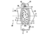
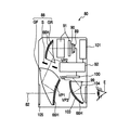
図21は、本発明の撮像装置の他の例を示す図で、自由曲面レンズ51(非回転対称面を有するレンズ)を用いたデジタルカメラ50の例である。52は可変焦点ミラー、53はアルミコーティングされた薄膜、54は電極、55は固体撮像素子、56は基板、57は電源、58はスイッチ、59は可変抵抗器である。
【0139】
可変焦点ミラー52の例としては、オプティックス コミュニケーションズ(Optics Communications),140巻(1997年)187頁乃至190頁に示されているメンブレインミラーがあり、電極54の間に電圧を印加すると静電気力により薄膜53を変形させて反射鏡の焦点距離が変化する。そしてピント調整ができる。物体からの光60は自由曲面プリズム51の面R1、R2で屈折され、反射鏡(薄膜)53にて反射され、自由曲面プリズム51の面R3で反射され、面R4で屈折されてから固体撮像素子55に入射する。
【0140】
このように、この装置は、自由曲面R1、R2、R3、R4および反射鏡53とにより撮像光学系を構成する。特に自由曲面R1、R2、R3、R4の形状を最適化することにより物体像の収差を最小にしている。
【0141】
図21の撮像装置において、反射鏡の開口の形状は、非点収差等を補正するためにY軸方向に長い楕円形にするのがよい。反射鏡52への入射光と反射鏡52からの出射光を含む平面と反射鏡52との交線の方向に長い楕円形にするのがよい。又、この図に示す例では、反射鏡52と薄膜53と固体撮像素子55とを別体で作って基板56上に配置している。しかし、反射鏡52および薄膜53をシリコンリソグラフィープロセス等で作ることもできるので基板56をシリコンにて形成し、固体撮像素子55と共にリソグラフィープロセスで反射鏡52の少なくとも一部を基板56上に形成してもよい。
【0142】
これによって、固体撮像素子55と共に反射鏡52とが一体化され小型化、低コスト化等の点で有利である。また反射鏡52は固定焦点のミラーとしても良い。この場合でも反射鏡52はリソグラフィープロセスで作ることができる。
【0143】
又、図示していないが、基板56上に反射型液晶ディスプレー又は透過型液晶ディスプレーをリソグラフィープロセスにより一体に形成してもよい。この基板56は、ガラスにて形成してもよく、このガラス基板上に薄膜トランジスター等の技術により固体撮像素子や液晶ディスプレーを形成すればよい。
【0144】
尚、自由曲面プリズム51は、プラスチックモールドやガラスモールド等にて形成することにより任意の所望形状の曲面を容易に形成することができ、製作も簡単である。
【0145】
図22は自由曲面プリズム51を用いたデジタルカメラの他の例である。このデジタルカメラは、図21に示すデジタルカメラにおける反射鏡52の代わりに可変焦点ミラー61を用いた例である。
【0146】
可変焦点ミラー61は、自由曲面プリズム51の面R2にこのプリズム51と一体に設けてある。この可変焦点ミラー61は、反射鏡62、自由曲面プリズムの面R2に形成した透明電極63と、配向膜64、65とよりなり、配向膜64、65との間に液晶66を設けたものである。
【0147】
ここで、可変焦点ミラー61は、自由曲面プリズム51とは別体にて形成し、両者を貼り合わせてもよく、又自由曲面プリズムの面R2に透明電極63と配向膜64とを形成してもよい。
【0148】
物体よりデジタルカメラへ入射する光60は、図21に示すカメラと同様に自由曲面プリズム51の面R1、R2にて夫々屈折され、その後反射鏡62にて反射され、配向膜64、液晶65、配向膜63、透明電極62を通って自由曲面プリズム51に入射し、面R3にて反射され面R4より出射して固体撮像素子55の受光面に入射する。ここで、可変焦点ミラー61に加える電圧を変化させることによりこのミラー61の焦点距離を変化させ、ピント調整することが可能である。
【0149】
この可変焦点ミラー61にて用いる液晶66には高分子分散液晶が用いられており、図15、図16、図17にもとづき説明したように、液晶分子に加わる電場を変化させることによって、例えば、図16に示す状態から図17に示す状態に変化し、これにより液晶の屈折率は変化し、可変焦点ミラーの焦点距離は変化する。
【0150】
この図22に示すデジタルカメラの実施の形態の場合、この図に示すように図16に示すデジタルカメラにて用いられている電極22、23は用いなくとも図16のデジタルカメラと同様の作用を有する。
【0151】
つまり図22において、スイッチ58がオフの場合、液晶の配列はランダムであり、屈折率の高い状態にある。したがって可変焦点ミラー61は光を収束させる作用が強い。ここでスイッチ58をオンにすると液晶は一方向に揃った配列になるので、屈折率は低くなり、光を収束させる作用は弱くなる。したがって可変焦点ミラー61は焦点調整が行なわれる。
【0152】
また可変焦点ミラー61を自由曲面プリズム51に二つ以上用いることによりズームレンズとして用いることが可能になる。
【0153】
又、図21に示すデジタルカメラの可変焦点ミラー52を図22に示す可変焦点ミラー61におき代えてもよい。又配向膜64、65は用いなくともよい。
【0154】
又、可変焦点ミラー61の液晶光学素子として透明電極63を電極を兼ねた反射鏡62で代用してもよい。
【0155】
また高分子分散液晶66の替わりに螺旋配向のネマチック液晶、コレステリック液晶、スメクチック液晶等を用いてもよい。
【0156】
図23は、図21又は図22に示すデジタルカメラにおける反射鏡53又は可変焦点ミラー61の代わりに回折光学素子70を用いた例である。つまり回折光学素子70は反射鏡72上に形成された回折面71と透明電極73、配向膜74と、液晶75とより構成されている。
【0157】
この図23に示すデジタルカメラ76は、物体よりの光が、他の例と同様に自由曲面プリズムに入射し、プリズム51を透過後回折光学素子70に入射し、ここで回折面71にて回折作用を受けた後に回折光学素子70を射出して再び自由曲面プリズム51に入射し、図示するように反射してからこれより射出して固体撮像素子55に入射する。
【0158】
ここでスイッチ77をオンにすると液晶分子の配向が垂直方向に変わり回折光学素子70の回折次数が変化するために焦点距離が変化してフォーカシングを行なうことができる。
【0159】
ここで液晶分子のピッチは、図12に示す液晶と同様に式(6)を満足する。又この例は、回折面71が反射面になっており、反射型の回折光学素子の例である。
【0160】
図24は図12に示す可変焦点レンズを用いた可変焦点眼鏡の例である。つまり眼鏡レンズとして可変焦点レンズを用いたもので、レンズ30H、31Hと配向膜(図示せず)と電極3等よりなる可変焦点レンズを眼鏡枠80に取り付けた構成である。
【0161】
尚図において、8、18は交流電源、9、24はスイッチ、13、17は可変抵抗、25は液晶である。又Pはピッチである。
【0162】
この可変焦点レンズは、電極22、23が図15に示すものと同様にレンズ30H、31Hの周辺部に設けられている。この電極22、23を透明電極にすれば、眼鏡の視野の周辺が明るくなり好ましい。
【0163】
以上述べた本発明の実施の形態は、光学特性可変光学素子として主として可変焦点レンズを用いたものであるが、光学特性可変光学素子として、回折光学素子、フレネルレンズ、プリズム、レンチキュラーレンズ等を用いてもよい。夫々の素子を構成する光の屈折又は反射する部分を屈折率可変物質つまり種々の液晶、強誘電体、電気光学効果を持つ物質にておきかえればよい。
【0164】
又、液晶の分子配向を変化させるために電場以外に磁場、電場の周波数、磁場の周波数を変化させてもよい。
【0165】
以上述べた本発明の光学特性可変光学素子を用いた光学系は、物体像を形成しその像をCCDや銀塩フィルムといった撮像素子に受光させて撮影を行なう撮影装置、とりわけカメラや内視鏡に用いることができる。また、物体像を接眼レンズを通して観察する観察装置、とりわけカメラのファインダー部の対物光学系としても用いることが可能である。以下に、その実施形態を例示する。
【0166】
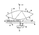
図25、26、27は、第5の実施の形態で本発明の光学特性可変光学素子を含む結像光学系を電子カメラのファインダー部の対物光学系に組み込んだ構成の概念図を示す。これらの図のうち図25は電子カメラ80の外観を示す前方斜視図、図26は同後方斜視図、図27は電子カメラ80の構成を示す断面図である。電子カメラ80は、この実施の形態では、撮影用光路82を有する撮影光学系81、ファインダー用光路84を有するファインダー光学系83、レリーズ85、フラッシュ86、液晶表示モニター87等を含み、カメラ80の上部に配置されたレリーズ85を押圧すると、それに連動して撮影用対物光学系88を通して撮影が行なわれる。撮影用対物光学系は、透過型の光学特性可変光学素子(ここでは液晶を用いている)を、複数備えており、ズーミングやフォーカシング作用を行なう。撮影用対物光学系88によって形成された物体像が、ローパスフィルター、赤外カットフィルター等のフィルタ91を介してCCD89の撮像面90上に形成される。このCCD89で受光された物体像は、処理手段92を介し、電子画像としてカメラ背面に設けられた液晶表示モニター87に表示される。また、この処理手段92にはメモリー等が配置され、撮影された電子画像を記録することもできる。なお、このメモリーは処理手段92と別体に設けてもよいし、フロッピーディスク等により電子的に記録書き込みを行なうように構成してもよい。またCCD89の代わりに銀塩フィルムを配置した銀塩カメラとして構成してもよい。
【0167】
さらに、ファインダー用光路84には、反射型光学特性可変光学素子を備えた結像光学系をファインダー用対物光学系として配置してある。また、カバー部材として正のパワーを有するカバーレンズ94を配置し、画角を拡大している。なお、このカバーレンズ94と結像光学系の絞りSより物体側のプリズムVP1とでファインダー用対物光学系93の前群GFを、結像光学系の絞りSより像側のプリズムVPでファインダー用対物光学系93の後群GRを構成している。絞りSを挟んだ前群GFと後群GRのおのおのに、光学特性可変光学素子を配置することにより、ズーミングとフォーカシングを行なっている。ここでは、反射プリズムと一体形成した、反射型の光学特性可変光学素子を用いている。ここでは、液晶66Hを用いているが、前述した通り光学特性を変化させることによりズーミングとフォーカシングの操作を行なっている。この制御は、処理手段により撮影用対物光学系のズーミング、フォーカシング作用に連動して行なわれる。このファインダー用対物光学系93によって形成された物体像は、像正立部材であるポロフリズム95の視野枠97上に形成される。尚、視野枠97は、ポロプリズム95の第1反射面96と第2反射面98との間を分離し、その間に視野枠97は配置されている。このポリプリズム95の後方には、正立正像にされた像を観察者眼球Eに導く接眼光学系99が配置されている。
【0168】
このように構成されたカメラ80は、ファインダー用対物光学系93を少ない光学部材で構成でき、高性能及び小型化が実現できると共に、対物光学系93の光路自体を折り曲げて構成できるため、カメラ内部での配置の自由度が増し、設計上有利となる。
【0169】
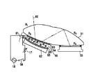
次に、図28は、本発明の結像光学系を電子カメラ80の撮影部の対物光学系88に組み込んだ構成の概念図を示す。この例の場合、撮影用光路82上に配置された撮影用対物光学系88は、反射型の光学特性可変光学素子を用いた結像光学系である。この撮影用対物光学系により形成された物体像は、ローパスフィルター、赤外カットフィルター等のフィルタ91を介してCCD89の撮像面90上に形成される。このCCD89で受光された物体像は、処理手段92を介し、液晶表示素子(LCD)100上に電子像として表示される。また、この処理手段92は、CCD89で撮影された物体像を電子情報として記録する記録手段101の制御も行なう。LCD100に表示された画像は、接眼光学系99を介して観察者の眼Eに導かれる。この接眼光学系99は、本発明の結像光学系に用いられているものと同様の形態を持つ光学特性可変光学素子を備えた偏芯プリズムからなり、前記光学素子の特性を変化させることにより観察者の視度に合わせてLCDの虚像の奥行きを調整可能としている。この例では入射面102と、反射面103と、反射と屈折とを兼用する面104の3面から構成されている。また、2つの反射作用を持った面103、104のうち少なくとも一方の面、望ましくは両方の面が、光束にパワーを与え、かつ、偏芯収差を補正する唯一の対称面を持つ面対称自由曲面にて構成されている。そして、この唯一の対称面は、撮影用対物光学系88の前後の群GF、GRに配置された偏芯プリズム、VP1、VP2が有する面対称自由曲面の唯一の対称面と略同一平面上に形成されている。ここでも液晶66Hを用いた反射型の光学特性可変光学素子が用いられている。
【0170】
このように構成されたカメラ80は、撮影用対物光学系88を少ない光学部材で構成でき、高性能で小型にできると共に、光学系全体を同一平面上に並べて配置できるため、この配置平面と垂直方向の厚みの薄型化が実現できる。
【0171】
次に、図29は、本発明の光学特性可変光学素子を電子内視鏡の観察系の対物光学系120に組み込んだ構成の概念図を示す。この例の場合も、観察系の対物光学系125は、ズーミングフォーカシングを行なう反射型光学特性可変光学素子128を備えた結像光学系を用いている。これら反射型光学特性可変光学素子は液晶66Hが用いられている。この電子内視鏡は、図29(A)に示すように、電子内視鏡111と、照明光を供給する光源装置112と、その電子内視鏡111に対応する信号処理を行なうビデオプロセッサ113と、このビデオプロセッサ113から出力される映像信号を表示するモニター114と、このビデオプロセッサ113と接続され映像信号等に記録するVTRデッキ115、および、ビデオディスク116と、映像信号を映像としてプリントアウトするビデオプリンタ117と共に構成されており、電子内視鏡111の挿入部118の先端部119は、図29(B)に示すように構成されている。光源装置112から照明された光束は、ライトガイドファイバー束126を通って照明用対物光学系127により、観察部位を照明する。そして、この観察部位からの光が、カバー部材124を介して、観察用対物光学系125によって物体像として形成される。この物体像は、ローパスフーフィルター、赤外カットフィルター等のフィルター121を介してCCD122の撮像面123上に形成される。さらに、この物体像は、CCD122によって映像信号に変換され、その映像信号は、図29(A)に示すビデオプロセッサ113により、モニター114上に直接表示されると共に、VTRデッキ115、ビデオディスク116中に記録され、また、ビデオプリンタ117から映像としてプリントアウトされる。
【0172】
このように構成された内視鏡は、ズーミングや、フォーカシング機能を備えているにもかかわらず、少ない光学部材で構成でき、高性能・小型化が実現できる。
【0173】
また、以上のプリズムを複数用いた実施の形態の結像光学系の前群や後群に設けられた偏芯プリズムとしては、何れも光学面3面からなり、その中の1面が全反射作用と透過作用とを兼用する面で構成された内部反射回数2回のタイプのプリズムを用いたが、本発明に用いる偏芯プリズムはこれに限られるものではない。
【0174】
本発明に用いることができるいくつかの可変焦点プリズムVPの例を図30〜図32に示す。なお、いずれも像面136に結像するプリズムVPとして説明するが、光路を逆にして像面136側から被写体からの光線が入射し、瞳131側に結像するプリズムVPとしても使用することができる。又単体で結像光学系や、観察光学系として構成してもよい。又、どの面に光学特性可変光学素子を用いるかは、使用形態により決定してよい。
【0175】
図30の場合は、プリズムVPは第1面132、第2面133、第3面134、第4面135からなり、入射瞳131を通って入射した光は、第1面132で屈折してプリズムVPに入射し、第2面133で内部反射し、第3面134に入射して内部反射し、第4面135に入射して屈折されて、像面136に結像する。光学特性可変光学素子を第3面134と第2面133に設けることにより、ズーミングとフォーカシングを可能としている。
【0176】
図31の場合は、プリズムVPは第1面132、第2面133、第3面134、第4面135からなり、入射瞳131を通って入射した光は、第1面132で屈折してプリズムVPに入射し、第2面133で内部反射し、第3面134に入射して全反射し、第4面135に入射して内部反射し、再び第3面134に入射して今度は屈折されて、像面136に結像する。ここでは、第2面133と第4面135に光学特性可変光学素子を用いた。
【0177】
図32の場合は、プリズムVPは第1面132、第2面133、第3面134、第4面135からなり、入射瞳131を通って入射した光は、第1面132で屈折してプリズムVPに入射し、第2面133で内部反射し、第3面134に入射して内部反射し、第2面133に再度入射して内部反射し、第4面135に入射して屈折されて、像面136に結像する。ここでは第2面133と第3面134に光学特性可変光学素子を用いた。
【0178】
又、本発明の光学特性可変光学素子は、画像表示装置に利用することができる。この画像表示装置を用いた第6の実施の形態として、図33に頭部装着型の画像表示装置を観察者頭部に装着した状態を、図34にその断面図を示す。この構成は、本発明の反射型光学特性可変光学素子を視度調節のために用いた偏芯プリズム光学系を図34に示すように接眼光学系140として用いており、接眼光学系140と画像表示素子141からなる組みを左右一対用意し、それらを眼輻距離だけ離して支持することにより、両眼で観察できる据え付け型又は頭部装着型画像表示装置のようなポータブル型の画像表示装置142として構成されている。
【0179】
すなわち、表示装置本体142には、上記のような接眼光学系140が左右一対備えられ、それらに対応して像面に液晶表示素子からなる画像表示素子141が配置されている。そして、表示装置本体142には、図33に示すように、左右に連続して図示のような側頭フレーム143が設けられ、表示装置本体142を観察者の眼前に保持できるようになっている。
【0180】
また、側頭フレーム143にはスピーカー144が付設されており、画像観察と共に立体音響を聞くことができるようになっている。このようにスピーカー144を有する表示装置本体142には、映像音声伝達コード145を介してポータブルビデオカセット等の再生装置146が接続されているので、観察者はこの再生装置146を図示のようにベルト箇所等の任意の位置に保持して、映像音響を楽しむことができるようになっている。図33の符号147は再生装置146のスイッチ、ボリューム等の調節部である。なお、表示装置本体142の内部に映像処理、音声処理回路等の電子部品を内蔵させてある。
【0181】
なお、コード145は先端をジャックにして、既存のビデオデッキ等に取り付け可能としてもよい。さらに、TV電波受信用チューナーに接続してTV鑑賞用としてもよいし、コンピュータに接続してコンピュータグラフィックスの映像や、コンピュータからのメッセージ映像等を受信するようにしてもよい。又、邪魔なコードを排斥するために、アンテナを接続して外部からの信号を電波によって受信するようにしてもよい。
【0182】
本発明において、特許請求の範囲に記載するもののほか下記の各項に記載するものもその目的に寄与する。
【0183】
(1) 電気光学効果又は磁気光学効果を持つ物質に電場又は磁場を加えることにより前記物質の屈折率を変化させて光学特性を変化させることを特徴とする光学特性可変光学素子。
【0184】
(2) 入射光軸にほぼ垂直な面内での液晶分子の方位が前記面内でほぼ均一な液晶に電場又は磁場または温度を加えることにより液晶の屈折率を変化させて光学特性を変化させるようにしたことを特徴とする光学特性可変光学素子。
【0185】
(3) 前記(1)の項に記載する光学特性可変光学素子を用いた可変焦点レンズ。
【0186】
(4) 電気光学効果を持つ物質の入射光軸にほぼ垂直な面内で方位が前記面内でほぼ均一である物質をもちい、前記物質の屈折率を変化させることにより光学特性を変化させることを特徴とする光学特性可変光学素子。
【0187】
(5) 前記(2)の項に記載する光学素子で、前記液晶の方位を規制する部材を備え、前記部材を描画露光とエッチングあるいはリソグラフィー技術を用いて加工したことを特徴とする光学特性可変光学素子。
【0188】
(6) 電気光学効果を持つ物質あるいは前記磁気光学効果を持つ物質の方位を規制するための部材を設け、前記部材が描画露光とエッチングあるいはリゾグラフィー技術を用いて加工したことを特徴とする光学特性可変光学素子。
【0189】
(7) 前記の(5)又は(6)の光学素子で、前記方位を規制する部材が下記条件(4)を満足することを特徴とする光学特性可変光学素子。
0.5nm<S<λ (4)
【0190】
(8) 液晶素子よりなり、液晶が負の屈折率異方性を持つことを特徴とする光学特性可変光学素子。
【0191】
(9) 液晶素子と、前記液晶素子の光軸とほぼ直交する方向に電場を加える部材とを備え、前記部材による電場が時間と共に方向を変化させるようにしたことを特徴とする光学特性可変光学素子。
【0192】
(10) 液晶素子と、前記液晶素子の光軸とほぼ平行な方向に電場を加える部材と、前記液晶素子の光軸とほぼ直交する方向に電場を加える部材とを備えたことを特徴とする光学特性可変光学素子。
【0193】
(11) 前記の(7)、(8)、(9)又は(10)に記載する光学素子で、下記式(7)を満足することを特徴とする光学特性可変光学素子。
T≦τ (7)
【0194】
(12) 前記(11)の項に記載する光学素子で、条件(7)の代りに下記条件式(7−1)を満足することを特徴とする光学特性可変光学素子。
T≦10τ (7−1)
【0195】
(13) 前記の(1)、(7)、(8)、(9)、(10)、(11)又は(12)の項に記載する光学素子で、前記光学素子が螺旋状の配向の液晶であることを特徴とする光学特性可変光学素子。
【0196】
(14) 前記の(13)の項に記載する光学素子で、下記式(6)、(5−61)、(5−62)、(5−28)、(5−29)、(5−30)のいずれかを満足することを特徴とする光学特性可変光学素子。
P<λ (6)
P<20π・λ≒62.8λ (5−61)
P<20λ (5−62)
|Γ/2Φ|<1 (5−28)
|Γ/2Φ|<π/6 (5−29)
|Γ/2Φ|<π (5−30)
【0197】
(15) 前記の(1)、(7)、(8)、(9)、(10)、(11)又は(12)の項に記載する光学素子で、光学素子として高分子分散液晶素子を用いたことを特徴とする光学特性可変光学素子。
【0198】
(16) 下記式(8)、(8−1)(9)、(9−1)のうちの少なくとも一つの式を満足することを特徴とする高分子分散液晶を用いた光学特性可変光学素子。
D<λ/5 (8)
D<2λ (8−1)
0.5<ff<0.999 (9)
0.1<ff<0.5 (9−1)
【0199】
(17) 前記(15)の項に記載する光学素子で、下記式(8−1)、(9−1)のうちの少なくとも一つの式を満足することを特徴とする光学特性可変光学素子。
D<2λ (8−1)
0.1<ff<0.5 (9−1)
【0200】
(18) 温度変化により液晶相と液体の相転移を起こし、屈折力を変える光学特性可変光学素子。
【0201】
(19) 前記の(1)、(2)、(3)、(4)、(5)、(6)、(7)、(8)、(9)、(10)、(11)、(12)、(13)、(14)、(15)、(16)又は(17)の項に記載する光学素子で、強度可変の磁場を加えて液晶の配向方向を制御することを特徴とする光学特性可変光学素子。
【0202】
(20) 前記の(1)、(2)、(3)、(4)、(5)、(6)、(7)、(8)、(9)、(10)、(11)、(12)、(13)、(14)、(15)、(16)又は(17)の項に記載する光学素子で、電場の強さあるいは周波数を変化させることによって液晶の配向方向を制御することを特徴とする光学特性可変光学素子。
【0203】
(21) 前記の(1)、(2)、(3)、(4)、(5)、(6)、(7)、(8)、(9)、(10)、(11)、(12)、(13)、(14)、(15)、(16)又は(17)の項に記載する光学素子で、前記光学素子として電場の周波数によって誘電異方性が変化する液晶素子を用いたことを特徴とする光学特性可変光学素子。
【0204】
(22) 前記の(1)、(2)、(3)、(4)、(5)、(6)、(7)、(8)、(9)、(10)、(11)、(12)、(13)、(14)、(15)、(16)、(17)、(18)、(19)、(20)又は(21)の項に記載する光学素子で、光学素子として電気光学効果を有する物質、磁気光学効果を有する物質、強誘電体等のうちの一つを用いることを特徴とする光学特性可変光学素子。
【0205】
(23) 液晶に加わる電場の周波数を変化させることにより光学特性を変化させるようにしたことを特徴とする光学特性可変光学素子。
【0206】
(24) 前記の(23)の項に記載する光学素子で、光学素子として螺旋構造を持つ液晶を備え、下記式(6)、(5−26)、(5−28)、(5−29)、(5−30)、(5−61)、(5−62)、(5−63)、(5−64)、(5−65)、(5−66)、(5−67)、(5−68)のいずれかを満足することを特徴とする光学特性可変光学素子。
P<λ (6)
|Γ/2Φ|<0.11 (5−26)
|Γ/2Φ|<1 (5−28)
|Γ/2Φ|<π/6 (5−29)
|Γ/2Φ|<π (5−30)
P<20π・λ≒62.8λ (5−61)
P<20λ (5−62)
λ≦P<20λ (5−63)
λ≦Pかつ |Γ/2Φ|<π (5−64)
2λ≦P<20λ (5−65)
2λ≦Pかつ |Γ/2Φ|<π (5−66)
2/3λ≦P<20λ (5−67)
2/3λ≦Pかつ |Γ/2Φ|<π (5−68)
【0207】
(25) 前記の(23)又は(24)の項に記載する光学素子で、光学素子として正の屈折率異方性を持つ液晶を用いたことを特徴とする光学特性可変光学素子。
【0208】
(26) 特許請求の範囲の請求項1、2、3又は4あるいは、前記の(1)、(2)、(3)、(4)、(5)、(6)、(7)、(8)、(9)、(10)、(11)、(12)、(13)、(14)、(15)、(16)、(17)、(18)、(19)、(20)、(21)、(22)、(23)、(24)又は(25)の項に記載する光学特性可変光学素子を備えた撮像装置。
【0209】
(27) 前記の(1)、(2)、(3)、(4)、(5)、(6)、(7)、(8)、(9)、(10)、(11)、(12)、(13)、(14)、(15)、(16)、(17)、(18)、(19)、(20)、(21)、(22)、(23)、(24)又は(25)の項に記載する光学特性可変光学素子を備えた可変焦点眼鏡。
【0210】
(28) 前記の(1)、(2)、(3)、(4)、(5)、(6)、(7)、(8)、(9)、(10)、(11)、(12)、(13)、(14)、(15)、(16)、(17)、(18)、(19)、(20)、(21)、(22)、(23)、(24)又は(25)の項に記載する光学特性可変光学素子を備えた光学機器。
【0211】
(29) 螺旋構造を持つ液晶の配向を変化させることにより光学特性が変化する光学特性可変光学素子。
【0212】
(30) 前記の(29)の項に記載する光学素子で、下記式(6)、(5−26)、(5−28)、(5−29)、(5−30)、(5−61)、(5−62)、(5−63)、(5−64)、(5−65)、(5−66)、(5−67)、(5−68)のいずれかを満足することを特徴とする光学特性可変光学素子。
P<λ (6)
|Γ/2Φ|<0.11 (5−26)
|Γ/2Φ|<1 (5−28)
|Γ/2Φ|<π/6 (5−29)
|Γ/2Φ|<π (5−30)
P<20π・λ≒62.8λ (5−61)
P<20λ (5−62)
λ≦P<20λ (5−63)
λ≦Pかつ |Γ/2Φ|<π (5−64)
2λ≦P<20λ (5−65)
2λ≦Pかつ |Γ/2Φ|<π (5−66)
2/3λ≦P<20λ (5−67)
2/3λ≦Pかつ |Γ/2Φ|<π (5−68)
【0213】
(31) 前記(30)項に記載する光学特性可変光学素子を備えた撮像装置。
【0214】
(32) 前記(30)項に記載する光学特性可変光学素子を備えた観察装置。
【0215】
(33) 前記(30)項に記載する光学特性可変光学素子を備えた表示装置。
【0216】
(34) 前記(30)項に記載する光学特性可変光学素子を備えた眼鏡。
【0217】
(35) 前記の(31)の項に記載する撮像装置で、絞りと、絞りの近傍に配置された凹の作用を有する前記光学特性可変光学素子を含む前群と、前群より後方に配置されている少なくとも凹面と凸面とを有する後群とよりなる光学系を備えていることを特徴とする撮像装置。
【0218】
(36) 前記の(31)の項に記載する撮像装置で、絞りと、絞りの近傍に配置されている前記光学特性可変光学素子を含む前群と、前群より後方に配置されている少なくとも凹面と凸面とを有する後群とよりなる光学系を備えていることを特徴とする撮像装置。
【0219】
(37) 前記の(35)又は(36)の項に記載する撮像装置で、少なくとも一つの非球面を有することを特徴とする撮像装置。
【0220】
(38) 前記の(35)、(36)又は(37)の項に記載する撮像装置で、撮像面が前記光学系の像面に位置する撮像素子を有し、前記撮像素子に入射する主光線の角度が撮像素子の撮像面に対し90°±20°の範囲であることを特徴とする撮像装置。
【0221】
【発明の効果】
本発明によれば、光学特性可変光学素子を備えたことにより複雑な機構等を用いずに焦点距離等の光学特性が可変であり、又前記光学特性可変光学素子の他に屈折面を設けることにより、少ない光学素子で機械的構造の簡単な撮像装置を得ることができる。
【図面の簡単な説明】
【図1】 本発明の第1の実施の形態の構成を示す図
【図2】 屈折率の異方性が負の液晶の屈折率楕円体
【図3】 本発明の第1の実施の形態で電場を加えた状態を示す図
【図4】 液晶分子の配向状態を示す図
【図5】 液晶分子の配向状態を示す図
【図6】 配向膜に形成されているパターン
【図7】 配向膜に形成されている他のパターン
【図8】 本発明の第2の実施の形態の構成を示す図
【図9】 本発明の第2の実施の形態の構成を示す図
【図10】 図8、9の実施の形態でz軸方向より見た図
【図11】 本発明の第2の実施の形態の変形例
【図12】 本発明の第2の実施の形態の光学素子を用いた撮像装置を示す図
【図13】 図12の撮像装置でZ方向より見た図
【図14】 本発明の光学特性可変光学素子を用いた可変焦点光学系の構成を示す図
【図15】 本発明の光学素子を用いたズームレンズを備えた撮像装置を示す図
【図16】 液晶の代りにポリマーを用いた液晶素子を示す図
【図17】 液晶の代りにポリマーを用いた液晶素子を示す図
【図18】 本発明の第3の実施の形態の構成を示す図
【図19】 本発明の第3の実施の形態の構成を示す図
【図20】 本発明の光学素子で磁場により配向を変化させる例を示す図
【図21】 本発明の第4の実施の形態で可変焦点ミラーの構成を示す図
【図22】 本発明の第4の実施の形態の他の例を示す図
【図23】 本発明の第4の実施の形態の他の例を示す図
【図24】 本発明の光学素子を用いた可変焦点眼鏡である第5の実施の形態を示す図
【図25】 第6の実施の形態で本発明を適用した電子カメラの前方斜視図
【図26】 第6の実施の形態の後方斜視図
【図27】 第6の実施の形態の断面図
【図28】 第6の実施の形態の変形例
【図29】 第7の実施の形態で本発明を電子内視鏡に適用した例
【図30】 本発明に適用可能な偏芯プリズムの例
【図31】 本発明に適用可能な偏芯プリズムの他の例
【図32】 本発明に適用可能な偏芯プリズムの他の例
【図33】 本発明の光学特性可変光学素子を適用した画像表示装置
【図34】 図33の画像表示装置の断面図
【図35】 本発明の撮像装置により得られた画像を補正する電子回路を示す図
【図36】 従来の液晶レンズを用いた光学系の構成を示す図
【図37】 他の従来の液晶レンズを用いた光学系の構成を示す図[0001]
BACKGROUND OF THE INVENTION
The present invention relates to an imaging apparatus including an optical system including an optical characteristic variable optical element such as a variable focus lens, a variable focus diffractive optical element, a variable deflection prism, and a variable focus mirror.
[0002]
[Prior art]
A conventional variable focus lens uses a lens manufactured by polishing glass, and the focal length cannot be changed by the lens itself. For example, like a zoom lens of a camera, a part of a lens group is arranged in the optical axis direction. The mechanical structure is complicated in order to change the focal length.
[0003]
In order to eliminate such defects, it is necessary to change the focal length of the lens itself. For example, as shown in FIG. 36, an optical system using a polarizing
[0004]
When an optical system including the polarizing
[0005]
Here, as shown in FIG. 36, in the state where the
[0006]
On the other hand, as shown in FIG. 37, when the
[0007]
As described above, the optical system shown in FIGS. 36 and 37 changes its focal length by selectively applying an electric field to the
[0008]
[Problems to be solved by the invention]
In the optical system using the liquid crystal lens shown in FIGS. 36 and 37, it is necessary to dispose the polarizing
[0009]
In addition, since the utilization efficiency is low in this way, products to which this optical system can be applied are limited, and there is a disadvantage that it lacks versatility. Furthermore, there is a drawback that it takes time to change the focal length.
[0010]
Further, the optical characteristic variable optical element such as a liquid crystal lens has a feature that optical characteristics such as a focal length can be changed by one optical element. However, it is not preferable to use only the optical property variable optical element because spherical aberration, distortion, chromatic aberration, and the like occur.
[0011]
The present invention provides an image pickup apparatus including a small optical system in which optical characteristics are variable and various aberrations are favorably corrected by adding another curved surface to the optical characteristic variable optical element.
[0012]
[Means for Solving the Problems]
The imaging apparatus of the present inventionAn optical property variable optical element in which the optical property is changed by changing the orientation of the liquid crystal having a spiral structure, and includes the following formulas (5-63), (5-64), (5-65), (5- 66), (5-67), or (5-68) is satisfiedIt is characterized by that.
λ ≦ P <20λ (5-63)
λ ≦ P and | Γ / 2Φ | <π (5-64)
2λ ≦ P <20λ (5-65)
2λ ≦ P and | Γ / 2Φ | <π (5-66)
2 / 3λ ≦ P <20λ (5-67)
2 / 3λ ≦ P and | Γ / 2Φ | <π (5-68)
[0013]
DETAILED DESCRIPTION OF THE INVENTION
Next, embodiments of the optical property variable optical element of the present invention will be described.
[0014]
The first embodiment of the optical property variable optical element according to the present invention will be described as an example of a variable focus lens as the optical element. In FIG. 1, 1 is a liquid crystal having a negative refractive index anisotropy, 2 is an alignment film, 3 is a transparent electrode, and is provided on
[0015]
In the optical element having such a configuration, the liquid crystal 1 having negative refractive index anisotropy has a refractive index ellipsoid having a shape as shown in FIG. 2 and a relationship represented by the following formula (1). It is characterized by.
[0016]
ne<Nox, Ne<Noy (1)
Where neIs the refractive index of extraordinary rays, noxIs the refractive index of the x-direction polarization, noyIs the refractive index of the y-direction polarization.
[0017]
The liquid crystal 1 satisfies the following formula (2).
nox= Noy≡no (2)
Where noIs the refractive index of ordinary light.
[0018]
In such a varifocal optical element made of a liquid crystal having a negative refractive index anisotropy, when no voltage is applied, the
[0019]
At this time, the refractive index of the liquid crystal with respect to the incident light is noThus, the optical element acts as a convex lens.
[0020]
Next, when the switch 9 is turned on in FIG. 1, the direction of the
n = (ne+ No) / 2 (3)
[0021]
Due to such a decrease in refractive power, the element has a weak refractive power as a convex lens and a focal length is increased, thereby acting as a variable focus lens. Further, by changing the
[0022]
Here, the
[0023]
Therefore, it acts as a variable focus lens having the same focal length no matter what polarized light enters the optical element.
[0024]
Note that the liquid crystal 1 originally has a property having homeotropic alignment as shown in FIG. 1, and therefore the
[0025]
Further, in order to change the alignment of the
[0026]
Further, even if the
0.5nm <S <λ (4)
[0027]
Here, the wavelength λ is 350 nm to 700 nm in the case of visible light. That is, in the case of visible light, equation (4) is as follows.
0.5nm <S <700nm
[0028]
Further, in the case of near-infrared light, the wavelength λ is 650 nm to 1200 nm, and therefore equation (4) can be expressed as follows.
0.5nm <S <1200nm
[0029]
In order to align the
[0030]
6 may be used instead of the pattern shown in FIG. 6 as long as the orientations of the
[0031]
This pattern is not an
[0032]
Thus, the liquid crystal lens that does not blur regardless of the polarization by averaging the orientation of the
ne> No (5)
[0033]
In addition, substances having electro-optic effect and magneto-optic effect such as polymer-dispersed liquid crystal, chiral smectic liquid crystal, chiral cholesteric liquid crystal, ferroelectric liquid crystal, anti-dielectric liquid crystal, and ferroelectric can also be applied to the present invention.
[0034]
Each of the above-described substances can be applied to embodiments described in detail later in addition to the embodiment of the present invention.
[0035]
FIG. 8 and FIG. 9 are diagrams showing another second embodiment of the present invention, and an example of a liquid crystal lens in which the orientation change of the
[0036]
In these figures, the
[0037]
In this variable focus lens, that is, a liquid crystal lens, FIG. 8 shows a state in which the switch 9 is on and the
[0038]
In order to change the focal length of the
[0039]
FIG. 10 is a view of the liquid crystal
[0040]
FIG. 11 is a modification of the second embodiment shown in FIGS. 8, 9, and 10, and is a modification in which the positions and shapes of the
[0041]
The second embodiment shown in FIG. 8 and the like is characterized in that the response speed when the z-axis of the
[0042]
The
[0043]
Further, the focal length of the
[0044]
In the above description, the dielectric anisotropy of the
[0045]
An example of such a liquid crystal is a discotic liquid crystal.
[0046]
Further, in the second embodiment shown in FIG. 8 and the like, the liquid crystal lens using the nematic
ne> No (5)
[0047]
The nematic
[0048]
FIG. 12 shows a digital camera imaging apparatus using the variable focus lens. In the variable focus lens used in the imaging apparatus shown in FIG. 12, the direction of one
[0049]
Assume that the pitch P is equal to or smaller than the wavelength λ, that is, as shown by the following formula (6).
P <λ (6)
[0050]
Then, this liquid crystal approaches an isotropic medium. The reason is described below.
[0051]
Assume that the following condition (5-1) is satisfied.
P << λ (5-1)
[0052]
Thus, when the pitch P is very small compared to the wavelength λ of light, the liquid crystal acts as a medium having a refractive index n ′ given by (5-2) below, regardless of the polarization of the incident light.
n '= (ne+ No) / 2 (5-2)
[0053]
Next, the reason why the nematic liquid crystal according to this embodiment behaves as an isotropic medium having a refractive index n ′ will be described with reference to Jones vectors and matrices.
[0054]
According to the formula shown on pages 85-92 of "Basics of Liquid Crystal and Display Applications", co-authored by Katsumi Yoshino and Masanori Ozaki, published by Corona Inc., when an absolute phase change exp (-iα) is included, Jones matrix W for nematic liquid crystal with thickness d shown in FIG.tIs given by the following equation (5-3).
However, Φ, Γ, α, X, and R (−Φ) are the following formulas (5-4), (5-5), (5-6), (5-7), and (5-8), respectively. Street.
Φ = 2πd / P (5-4)
[0056]
In addition, Φ represents the twist angle of the liquid crystal molecules of nematic liquid crystal in radians. In addition, the coordinate systems of the equations (5-3) and (5-8) are assumed to be the x, y, and z axes shown in FIG. That is, the x-axis is from the front to the back of the page, and the y-axis is the direction of the major axis of the liquid crystal molecules at the incident surface of the chiral nematic liquid crystal. Under the condition of Expression (5-1), W in Expression (5-3)tLet's examine what happens.
[0057]
Expression (5-1) can be transformed into the following expression (5-9).
0 <P / λ << 1 (5-9)
[0058]
Therefore, when p /
[0059]
Γ / Φ is given by (5-10).
Γ / Φ = (ne-No) (P / λ) (5-10)
[0060]
Therefore, when P / λ << 1, Γ / Φ is as shown in Equation (5-11).
[0061]
| Γ / Φ | << 1 (5-11)
[0062]
Therefore, when P /
[0063]
Under the condition of the expression (5-11), X in the expression (5-7) becomes as shown in the following expressions (5-12), (5-13), and (5-14).
X → Φ (5-16)
cosX → cosΦ (5-17)
This is because the refractive index n '= (ne+ No) / 2, a thickness d and a Jones matrix of an isotropic medium along the optical axis.
[0065]
Therefore, since P / λ << 1, the
[0066]
Even when the liquid crystal has an intermediate arrangement as shown in FIG.eThe value of neAnd noThe refractive index n of extraordinary light which is an intermediate value ofeIt is possible to satisfy the above expressions (5-3) to (5-20) by replacing with '.
[0067]
12 is not limited to continuously variable voltage application, the variable focus lens can be selected from several discrete voltage values. realizable.
[0068]
Here, a practical example of the variable focus lens having the configuration as shown in FIG. 12 will be described in detail.
[0069]
Although the limit case of P / λ → 0 is shown in Expression (5-20), the limit value may not always be applied to an actual liquid crystal lens and variable focus lens, so Expression (5-3) Let's derive an approximate expression of P / λ <1 may not be satisfied.
[0070]
The equation (5-3) is approximated by considering up to the first order of P / λ. That is, in equations (5-12) to (5-14), up to the first order of P / λ, that is, up to the first order of Γ / Φ from equation (5-10), and the second order of Γ / Φ. If the above is omitted, equation (5-21) is obtained.
From these formulas (5-20), (5-21), and (5-22), the following formula (5-23) is obtained.
Therefore, WtNCan be regarded as almost equal to the Jones matrix of the isotropic medium, it is sufficient that | i · Γ / 2Φ | is close to zero. At this time WtNApproaches the following formula (5-24).
This expression (5-24) means that the liquid crystal rotates by the polarization direction Γ / 4 · Γ / Φ of incident light, but can be regarded as an isotropic medium.
[0074]
Therefore, if the expression (5-25) is satisfied, that is, if the expression (5-26) is approximately satisfied, a variable focus lens that is not blurred can be obtained.
[0075]
| I · (Γ / 2Φ) | ≈0 (5-25)
| Γ / 2Φ | <0.11 (5-26)
From equation (5-10), Γ / 2Φ is represented by the following equation (5-27).
When the variable focus lens of the present invention is used for a lens of a relatively low cost product such as an actual imaging device with a lens, for example, an electronic camera, a VTR camera, an electronic endoscope, etc., the number of pixels of the solid-state imaging device is small, Since high resolution may not be required in some cases, the condition of Expression (5-26) can be relaxed and the following condition (5-28) may be satisfied.
| Γ / 2Φ | <1 (5-28)
[0077]
High resolution is required for a lens of an electronic imaging device having a large number of pixels, a film camera, a lens of a high-quality product such as a microscope, and so it is desirable to satisfy the following condition (5-29).
| Γ / 2Φ | <π / 6 (5-29)
[0078]
In the case of a lens that is not used for image formation, such as an optical disk lens, or an electronic imaging device that has a small number of pixels, the conditions are further relaxed, and the following condition (5-30) may be satisfied.
| Γ / 2Φ | <π (5-30)
[0079]
Note that, in common with this embodiment, when the liquid crystal is in a spiral arrangement, when the major axis direction of the liquid crystal molecules is not perpendicular to the optical axis, that is, when it is oblique, the equation (5) -1), n in formula (5-26) to formula (5-30)eN aboveeYou can replace it with '.
[0080]
Next, a design example is described.
[0081]
If the thickness d of the nematic liquid crystal is thin, the power of the lens is weak and is not useful. If it is thick, the light scatters and causes flare. Therefore, it is desirable that the thickness d satisfies the following condition (5-31).
2μ <d <300μ (5-31)
[0082]
The wavelength λ of the light is in the range of the following condition (5-32) when considering visible light.
0.35 μ <λ <0.7 μ (5-32)
[0083]
Ne-NoThe value of is determined by the physical properties of the liquid crystal, and there are many substances in the following range (5-33).
0.01 <| ne-No| <0.4 (5-33)
[0084]
Next, the following first to fourth design examples are shown as design examples.
First design example
d = 15 μ
λ = 0.5μ
ne-No= 0.2
P = 0.06μ
Therefore
Γ / 2Φ = (1/2) · 0.2 × 0.06 / 0.5 = 0.012
Thus, Expression (5-20), Expression (5-28), Expression (5-29), and Expression (5-30) are satisfied.
[0085]
Second design example
d = 50μ
λ = 0.6μ
ne-No= 0.25
P = 0.5μ
Therefore
Γ / 2Φ = (1/2) · 0.5 × 0.25 / 0.6 = 0.1022
Thus, Expression (5-26), Expression (5-28), Expression (5-29), and Expression (5-30) are satisfied.
[0086]
Third design example
d = 100μ
λ = 0.55μ
ne-No= 0.2
P = 3μ
Therefore
Γ / 2Φ = (1/2) · 0.2 × 3 / 0.55 = 0.5454
Thus, the expressions (5-28) and (5-30) are satisfied.
[0087]
Fourth design example
d = 200μ
λ = 0.95μ
ne-No= 0.2
P = 7μ
Therefore
Γ / 2Φ = (1/2) · 0.2 × 7 / 0.95 = 0.737
Thus, the expressions (5-28) and (5-30) are satisfied.
[0088]
In each of the above design examples, the chiral nematic liquid crystal has been described as an example. However, in order to make the wavelength smaller than the wavelength of light using the helical pitch of the nematic liquid crystal, a chiral agent may be mixed with the liquid crystal.
[0089]
As the chiral agent, a cholesteric liquid crystal or a synthetic optically active compound is used. The following chemical formulas (1) and (2) are examples of nematic liquid crystals, and chemical formulas (3) and (4) are examples of chiral agents.
In the above formula (5-30), considering an example of a malleable liquid crystal
ne-No= 0.1 as
(1/2) × 0.1 (P / λ) <π
P <20π · λ≈62.8λ (5-61) is obtained.
Similarly ne-No= 0.1 is applied to the equation (5-28),
P <20λ (5-62) is obtained.
[0091]
Therefore, if the formula (5-61) or the formula (5-62) is satisfied by a product using liquid crystal, an optical characteristic variable optical element such as a variable focus lens with less blur (flare) can be obtained. The expressions (5-1) to (5-30) are not limited to nematic liquid crystals and apply to all liquid crystals having a helical structure with a pitch P. Examples of such liquid crystals include cholesteric liquid crystals, smectic liquid crystals, ferroelectric liquid crystals, and antiferroelectric liquid crystals.
In order to improve the performance of the optical system, the value of the pitch P is preferably small. However, in general, when the value of the pitch P is small in the liquid crystal, the viscosity of the liquid crystal increases, and the response speed of the change in the refractive index with respect to the change in the electric field becomes slow. In consideration of this point, the value of the pitch P is preferably larger than the wavelength λ as a result of the experiment, and the expressions (5-28), (5-29), (5-30), and (5- 61), formula (5-62), etc. are also taken into consideration, it is desirable to satisfy the following formula (5-63) or formula (5-64).
λ ≦ P <20λ (5-63)
λ ≦ P and | Γ / 2Φ | <π (5-64)
Further, in an optical system of an autofocus television camera or the like, a faster response speed is required. Therefore, in these optical systems, it is desirable to satisfy the following formula (5-65) or formula (5-66).
2λ ≦ P <20λ (5-65)
2λ ≦ P and | Γ / 2Φ | <π (5-66)
Conversely, in an optical system that does not require a very fast response speed, such as glasses or a diopter adjustment device, the following equation (5-67) or equation (5-68) may be satisfied.
2 / 3λ ≦ P <20λ (5-67)
2 / 3λ ≦ P and | Γ / 2Φ | <π (5-68)
The upper limit of the value of P in Expression (5-63), Expression (5-65), and Expression (5-67) is allowed to 60λ in an inexpensive optical system that does not require high optical performance, such as a camera finder. .
In the case of a chiral nematic liquid crystal having a thickness of 9 microns and P = 1.1 microns, the response time corresponding to the change in the alternating electric field was about 1 second or less to about 30 seconds.
[0092]
FIG. 13 is a view of the
[0093]
Next, the operation of the apparatus shown in FIGS. 12 and 13 will be described.
[0094]
First, when the switch 9 is on, the
[0095]
Next, when the switch 9 is turned off and the
[0096]
Further, the switching period T of the voltage applied to the three electrodes of the
[0097]
In the optical system shown in FIG. 12, when the switch 9 is turned off at a certain time while the
[0098]
As described above, when the time until the alignment naturally occurs as shown in FIG. 12 is τ, it is necessary to have the following relationship.
T ≦ τ (7)
If T is too large and the above (7) is not satisfied, the spiral of the
[0099]
The above formula (7) may satisfy the following formula (7-1) practically.
T ≦ 10τ (7-1)
This is because, if this formula (7-1) is not satisfied, it may take time for the
[0100]
Note that the
[0101]
As shown in FIG. 14, the focal length of the
[0102]
FIG. 15 is a diagram showing the third embodiment, and is an example in which the variable focus lens shown in FIGS. 12 to 14 is used for a zoom lens. In the figure,
[0103]
In this example, instead of changing the electric field strength applied to the
[0104]
In this zoom lens, the frequency is changed by switching the
[0105]
Liquid crystal25b, 25GIn addition to the spiral liquid crystal, a polymer-dispersed liquid crystal in which a liquid crystal whose dielectric anisotropy changes with frequency is dispersed in a polymer may be used. The
[0106]
An AC power supply 9e capable of continuously changing the frequency is connected to the two
[0107]
Further, zooming can be performed by interlocking the
[0108]
The
[0109]
In the imaging apparatus shown in FIG. 12, instead of the
[0110]
The optical systems shown in FIGS. 16 and 17 are the same as the optical system shown in FIG.
[0111]
In the example shown in FIGS. 16 and 17, the divided
[0112]
In the optical system shown in FIGS. 16 and 17, the switch 9 is on, and the
[0113]
In this way, that is, as shown in FIG. 17, the arrangement of the
[0114]
Here, if the average diameter D of the
D <λ / 5 (8)
Where λ is the wavelength of incident light.
[0115]
When the thickness of the
D <2λ (8-1)
[0116]
Further, when the ratio of the
0.5 <ff <0.999 (9)
[0117]
The value of ff is the condition (9If the upper limit of 0.999) is exceeded, the amount of polymer decreases and
[0118]
When it is desired to make the
0.1 <ff <0.5 (9-1)
[0119]
FIG. 18 shows another embodiment of the optical system of the present invention, and shows an example of an optical system in which the refractive index of the liquid crystal is changed by changing the temperature.
[0120]
The nematic
[0121]
Next, the
[0122]
In the state shown in FIG. 19, the refractive index n of the
n = (2nO+ Ne) / 3 (10)
[0123]
That is, the refractive index n of the liquid crystal is increased, and as a result, the refractive power of the
[0124]
In the state of FIG. 18, the alignment regulating force by the
[0125]
In order to cause the liquid crystal to undergo a phase transition to a liquid, the optical systems shown in FIGS. 18 and 19 are heated using the
[0126]
The optical property variable optical element of the present invention described above is performed mainly by changing the strength and direction of the electric field in order to change the orientation of the molecules of the liquid crystal constituting the optical element.
[0127]
However, the orientation of the liquid crystal molecules can be changed by changing the frequency of the electric field applied to the liquid crystal without being limited to the change of the electric field strength. In addition, the orientation of liquid crystal molecules can be changed by changing the strength of the magnetic field.
[0128]
Further, the method of changing the orientation of the liquid crystal molecules by changing the frequency of the electric field applied to the liquid crystal and the method of changing the strength of the magnetic field applied to the liquid crystal are shown in FIGS. The present invention can be applied to each optical system shown as an example in FIG. 9, FIG. 12, FIG. 15, FIG. 16, FIG.
[0129]
In the method of changing the orientation of the liquid crystal molecules by changing the frequency of the electric field, the orientation of the liquid crystal molecules can be changed at a high speed by changing the frequency of the electric field if a liquid crystal with positive and negative dielectric anisotropies is used. It is advantageous.
[0130]
FIG. 20 shows an example of a lens whose refractive index is changed by the magnetic field H. In this figure, 45 is a lens, 46 is a substance having a magneto-optical effect, 47 is a substrate, 48 is an alignment film, 49A is a switch, 49B is an AC power supply, 49C is a variable resistor, 49D is a coil, and 49E is an iron core. .
[0131]
Examples of the material 46 having a magneto-optical effect to be used include lead glass, water length, and liquid crystal. The
[0132]
In order to change the alignment of the liquid crystal molecules at high speed, it is preferable to apply a certain voltage in advance instead of the voltage being off. When it is desired to change the alignment of the liquid crystal molecules, the alignment of the liquid crystal molecules can be changed at a high speed by setting the voltage to a higher voltage.
[0133]
The above-described example shown in FIG. 12 is an image pickup apparatus for a digital camera of the present invention using an optical characteristic variable optical element. This example will be described in more detail.
[0134]
In FIG. 12, the variable focus
[0135]
Further, when the orientation of the
[0136]
In the imaging apparatus shown in FIG. 12, the change in MTF due to the change in aberration and the change in light scattering is corrected by an electronic circuit. In other words, the compensation of the MTF change when the focal length of the
[0137]
FIG. 35 is a diagram for explaining the correction by the electronic circuit. In this figure, an example of performing distance measurement using an infrared light projection type active distance measurement method is shown. Based on the distance information obtained here, an enhancement amount or the like is selected to compensate for the MTF change of the liquid crystal lens. A digital filter is then applied to create the final image.
[0138]
FIG. 21 is a diagram showing another example of the imaging apparatus of the present invention, and is an example of a digital camera 50 using a free-form surface lens 51 (a lens having a non-rotationally symmetric surface). 52 is a variable focus mirror, 53 is an aluminum-coated thin film, 54 is an electrode, 55 is a solid-state imaging device, 56 is a substrate, 57 is a power source, 58 is a switch, and 59 is a variable resistor.
[0139]
As an example of the
[0140]
In this way, this apparatus has a free-form surface R1, R2, RThree, RFourThe reflecting
[0141]
In the imaging apparatus of FIG. 21, the shape of the opening of the reflecting mirror is preferably an ellipse that is long in the Y-axis direction in order to correct astigmatism and the like. It is preferable to make an ellipse that is long in the direction of the line of intersection between the reflecting
[0142]
As a result, the solid-
[0143]
Although not shown, a reflective liquid crystal display or a transmissive liquid crystal display may be integrally formed on the
[0144]
The free
[0145]
FIG. 22 shows another example of a digital camera using a free-
[0146]
The
[0147]
Here, the
[0148]
[0149]
As the
[0150]
In the case of the embodiment of the digital camera shown in FIG. 22, as shown in the figure, the same operation as that of the digital camera of FIG. 16 can be achieved without using the
[0151]
That is, in FIG. 22, when the
[0152]
Further, by using two or more variable focus mirrors 61 in the free-
[0153]
Further, the
[0154]
Further, as the liquid crystal optical element of the
[0155]
Further, instead of the polymer dispersed
[0156]
FIG. 23 shows an example in which a diffractive
[0157]
In the
[0158]
When the
[0159]
Here, the pitch of the liquid crystal molecules satisfies the formula (6) similarly to the liquid crystal shown in FIG. In this example, the
[0160]
FIG. 24 shows an example of variable focus glasses using the variable focus lens shown in FIG. That is, a variable focus lens is used as the spectacle lens, and the variable focus lens composed of the
[0161]
In the figure, 8 and 18 are AC power supplies, 9 and 24 are switches, 13 and 17 are variable resistors, and 25 is a liquid crystal. P is a pitch.
[0162]
In this variable focus lens, the
[0163]
The embodiment of the present invention described above mainly uses a variable focus lens as the optical characteristic variable optical element, but uses a diffractive optical element, a Fresnel lens, a prism, a lenticular lens, etc. as the optical characteristic variable optical element. May be. The light refracting or reflecting portions constituting each element may be replaced with a refractive index variable material, that is, various liquid crystals, ferroelectric materials, and materials having an electro-optic effect.
[0164]
In addition to the electric field, the magnetic field, the frequency of the electric field, and the frequency of the magnetic field may be changed in order to change the molecular orientation of the liquid crystal.
[0165]
The optical system using the optical property variable optical element of the present invention described above forms an object image, and the image is picked up by an image sensor such as a CCD or a silver salt film to take an image, especially a camera or an endoscope. Can be used. Further, it can also be used as an observation optical device for observing an object image through an eyepiece, particularly as an objective optical system of a camera finder. The embodiment is illustrated below.
[0166]
FIGS. 25, 26, and 27 are conceptual diagrams of a configuration in which the imaging optical system including the optical characteristic variable optical element of the present invention is incorporated in the objective optical system of the finder portion of the electronic camera in the fifth embodiment. 25 is a front perspective view showing the appearance of the
[0167]
Further, in the finder
[0168]
The
[0169]
Next, FIG. 28 shows a conceptual diagram of a configuration in which the imaging optical system of the present invention is incorporated in the objective
[0170]
In the
[0171]
Next, FIG. 29 shows a conceptual diagram of a configuration in which the optical characteristic variable optical element of the present invention is incorporated in the objective
[0172]
The endoscope configured as described above can be configured with a small number of optical members despite the zooming and focusing functions, and can achieve high performance and downsizing.
[0173]
The decentering prisms provided in the front group and the rear group of the imaging optical system according to the embodiment using a plurality of the above prisms each have three optical surfaces, one of which is totally reflected. Although a prism of the type having two internal reflections composed of a surface that serves both as an action and a transmission action is used, the eccentric prism used in the present invention is not limited to this.
[0174]
Examples of several variable focus prisms VP that can be used in the present invention are shown in FIGS. Although both are described as the prism VP that forms an image on the
[0175]
In the case of FIG. 30, the prism VP includes the
[0176]
In the case of FIG. 31, the prism VP includes the
[0177]
In the case of FIG. 32, the prism VP includes a
[0178]
The optical property variable optical element of the present invention can be used in an image display apparatus. As a sixth embodiment using this image display device, FIG. 33 shows a state in which a head-mounted image display device is attached to an observer's head, and FIG. 34 shows a cross-sectional view thereof. In this configuration, an eccentric prism optical system using the reflective optical property variable optical element of the present invention for diopter adjustment is used as an eyepiece
[0179]
That is, the display device
[0180]
In addition, a
[0181]
The
[0182]
In the present invention, in addition to what is described in the claims, what is described in the following items also contributes to the object.
[0183]
(1) A variable optical property optical element characterized by changing an optical property by applying an electric field or a magnetic field to a material having an electro-optic effect or a magneto-optic effect, thereby changing a refractive index of the material.
[0184]
(2) By changing the refractive index of the liquid crystal by changing the refractive index of the liquid crystal by applying an electric field, magnetic field or temperature to the liquid crystal in which the orientation of the liquid crystal molecules is substantially uniform in the plane substantially perpendicular to the incident optical axis, the optical characteristics are changed. An optical property variable optical element characterized by being configured as described above.
[0185]
(3) A variable focus lens using the optical property variable optical element described in the item (1).
[0186]
(4) Using a substance having a direction almost uniform in the plane substantially perpendicular to the incident optical axis of the substance having an electro-optic effect, and changing the optical characteristics by changing the refractive index of the substance. An optical property variable optical element characterized by the above.
[0187]
(5) The optical element described in the above item (2), comprising a member for regulating the orientation of the liquid crystal, wherein the member is processed by using drawing exposure and etching or lithography technology. Optical element.
[0188]
(6) An optical device characterized in that a member for regulating the orientation of a substance having an electro-optic effect or a substance having the magneto-optic effect is provided, and the member is processed by using drawing exposure and etching or a lithographic technique. Variable characteristic optical element.
[0189]
(7) The optical element according to (5) or (6), wherein the member for regulating the orientation satisfies the following condition (4).
0.5nm <S <λ (4)
[0190]
(8) An optical property variable optical element comprising a liquid crystal element, wherein the liquid crystal has negative refractive index anisotropy.
[0191]
(9) A variable optical characteristic optical system comprising: a liquid crystal element; and a member for applying an electric field in a direction substantially orthogonal to the optical axis of the liquid crystal element, and the electric field generated by the member changes its direction with time. element.
[0192]
(10) A liquid crystal element, a member for applying an electric field in a direction substantially parallel to the optical axis of the liquid crystal element, and a member for applying an electric field in a direction substantially orthogonal to the optical axis of the liquid crystal element are provided. Optical property variable optical element.
[0193]
(11) An optical element according to (7), (8), (9) or (10), wherein the following optical expression (7) is satisfied:
T ≦ τ (7)
[0194]
(12) An optical element according to the item (11), wherein the following conditional expression (7-1) is satisfied instead of the condition (7): An optical property variable optical element.
T ≦ 10τ (7-1)
[0195]
(13) The optical element according to the item (1), (7), (8), (9), (10), (11), or (12), wherein the optical element has a helical orientation. A variable-optical-characteristic optical element characterized by being a liquid crystal.
[0196]
(14) In the optical element described in the above item (13), the following formulas (6), (5-61), (5-62), (5-28), (5-29), (5- 30) Any one of the optical characteristic variable optical elements satisfying any of the above.
P <λ (6)
P <20π · λ≈62.8λ (5-61)
P <20λ (5-62)
| Γ / 2Φ | <1 (5-28)
| Γ / 2Φ | <π / 6 (5-29)
| Γ / 2Φ | <π (5-30)
[0197]
(15) The optical element according to the item (1), (7), (8), (9), (10), (11) or (12), wherein a polymer dispersed liquid crystal element is used as the optical element. A variable optical property optical element characterized by being used.
[0198]
(16) Optical property variable optical element using polymer dispersed liquid crystal satisfying at least one of the following formulas (8), (8-1), (9), and (9-1) .
D <λ / 5 (8)
D <2λ (8-1)
0.5 <ff <0.999 (9)
0.1 <ff <0.5 (9-1)
[0199]
(17) The optical element described in the above item (15), wherein at least one of the following formulas (8-1) and (9-1) is satisfied.
D <2λ (8-1)
0.1 <ff <0.5 (9-1)
[0200]
(18) A variable-optical-characteristic optical element that causes a phase transition between a liquid crystal phase and a liquid due to a temperature change and changes a refractive power.
[0201]
(19) (1), (2), (3), (4), (5), (6), (7), (8), (9), (10), (11), ( 12), (13), (14), (15), (16) or (17), wherein the alignment direction of the liquid crystal is controlled by applying a magnetic field of variable intensity. Optical property variable optical element.
[0202]
(20) (1), (2), (3), (4), (5), (6), (7), (8), (9), (10), (11), (11) 12), (13), (14), (15), (16), or (17), the liquid crystal orientation direction is controlled by changing the intensity or frequency of the electric field. An optical property variable optical element characterized by the above.
[0203]
(21) (1), (2), (3), (4), (5), (6), (7), (8), (9), (10), (11), (11) 12), (13), (14), (15), (16) or (17), the liquid crystal element whose dielectric anisotropy changes depending on the frequency of the electric field is used as the optical element. An optical property variable optical element characterized by that.
[0204]
(22) (1), (2), (3), (4), (5), (6), (7), (8), (9), (10), (11), (11) 12), (13), (14), (15), (16), (17), (18), (19), (20) or (21) as an optical element. An optical characteristic variable optical element using one of a substance having an electro-optic effect, a substance having a magneto-optic effect, and a ferroelectric substance.
[0205]
(23) An optical property variable optical element characterized in that the optical property is changed by changing the frequency of the electric field applied to the liquid crystal.
[0206]
(24) The optical element described in the above item (23), including a liquid crystal having a spiral structure as an optical element, and the following formulas (6), (5-26), (5-28), and (5-29): ), (5-30), (5-61), (5-62), (5-63), (5-64), (5-65), (5-66), (5-67), Any of (5-68) is satisfied, A variable optical property optical element characterized by the above-mentioned.
P <λ (6)
| Γ / 2Φ | <0.11 (5-26)
| Γ / 2Φ | <1 (5-28)
| Γ / 2Φ | <π / 6 (5-29)
| Γ / 2Φ | <π (5-30)
P <20π · λ≈62.8λ (5-61)
P <20λ (5-62)
λ ≦ P <20λ (5-63)
λ ≦ P and | Γ / 2Φ | <π (5-64)
2λ ≦ P <20λ (5-65)
2λ ≦ P and | Γ / 2Φ | <π (5-66)
2 / 3λ ≦ P <20λ (5-67)
2 / 3λ ≦ P and | Γ / 2Φ | <π (5-68)
[0207]
(25) A variable-optical-characteristic optical element characterized in that a liquid crystal having positive refractive index anisotropy is used as the optical element in the optical element described in the item (23) or (24).
[0208]
(26)
[0209]
(27) (1), (2), (3), (4), (5), (6), (7), (8), (9), (10), (11), (11) 12), (13), (14), (15), (16), (17), (18), (19), (20), (21), (22), (23), (24) Alternatively, varifocal glasses provided with the optical characteristic variable optical element described in the item (25).
[0210]
(28) The above (1), (2), (3), (4), (5), (6), (7), (8), (9), (10), (11), ( 12), (13), (14), (15), (16), (17), (18), (19), (20), (21), (22), (23), (24) Or an optical apparatus comprising the optical property variable optical element described in the item (25).
[0211]
(29) An optical property variable optical element in which optical properties are changed by changing the orientation of a liquid crystal having a spiral structure.
[0212]
(30) In the optical element described in the above item (29), the following formulas (6), (5-26), (5-28), (5-29), (5-30), (5- 61), (5-62), (5-63), (5-64), (5-65), (5-66), (5-67), or (5-68) is satisfied. An optical property variable optical element characterized by the above.
P <λ (6)
| Γ / 2Φ | <0.11 (5-26)
| Γ / 2Φ | <1 (5-28)
| Γ / 2Φ | <π / 6 (5-29)
| Γ / 2Φ | <π (5-30)
P <20π · λ≈62.8λ (5-61)
P <20λ (5-62)
λ ≦ P <20λ (5-63)
λ ≦ P and | Γ / 2Φ | <π (5-64)
2λ ≦ P <20λ (5-65)
2λ ≦ P and | Γ / 2Φ | <π (5-66)
2 / 3λ ≦ P <20λ (5-67)
2 / 3λ ≦ P and | Γ / 2Φ | <π (5-68)
[0213]
(31) An imaging device comprising the optical property variable optical element described in (30).
[0214]
(32) An observation apparatus comprising the optical property variable optical element described in (30).
[0215]
(33) A display device comprising the optical property variable optical element described in (30).
[0216]
(34) Glasses provided with the optical property variable optical element described in the above (30).
[0217]
(35) In the imaging device described in (31) above, a diaphragm, a front group including the optical characteristic variable optical element having a concave function disposed in the vicinity of the diaphragm, and a rear side of the front group An image pickup apparatus comprising an optical system including a rear group having at least a concave surface and a convex surface.
[0218]
(36) In the imaging device described in (31) above, at least a diaphragm, a front group including the optical characteristic variable optical element disposed in the vicinity of the diaphragm, and at least disposed behind the front group An imaging apparatus comprising an optical system including a rear group having a concave surface and a convex surface.
[0219]
(37) The imaging device according to (35) or (36), wherein the imaging device has at least one aspherical surface.
[0220]
(38) In the imaging apparatus according to (35), (36), or (37), the imaging surface includes an imaging element positioned on an image plane of the optical system, and is incident on the imaging element. An image pickup apparatus characterized in that an angle of light rays is in a range of 90 ° ± 20 ° with respect to an image pickup surface of an image pickup element.
[0221]
【The invention's effect】
According to the present invention, since the optical property variable optical element is provided, the optical characteristics such as the focal length can be changed without using a complicated mechanism, and a refractive surface is provided in addition to the optical property variable optical element. As a result, an image pickup apparatus having a simple mechanical structure can be obtained with a small number of optical elements.
[Brief description of the drawings]
FIG. 1 is a diagram showing a configuration of a first exemplary embodiment of the present invention
FIG. 2 A refractive index ellipsoid of a liquid crystal with negative refractive index anisotropy.
FIG. 3 is a diagram showing a state where an electric field is applied in the first embodiment of the present invention.
FIG. 4 is a diagram showing the alignment state of liquid crystal molecules
FIG. 5 is a diagram showing the alignment state of liquid crystal molecules
FIG. 6 shows a pattern formed on the alignment film.
FIG. 7 shows another pattern formed on the alignment film.
FIG. 8 is a diagram showing a configuration of a second exemplary embodiment of the present invention.
FIG. 9 is a diagram showing a configuration of a second exemplary embodiment of the present invention.
FIG. 10 is a diagram seen from the z-axis direction in the embodiment of FIGS.
FIG. 11 shows a modification of the second embodiment of the present invention.
FIG. 12 is a diagram showing an imaging apparatus using an optical element according to a second embodiment of the present invention.
13 is a diagram viewed from the Z direction in the imaging apparatus of FIG.
FIG. 14 is a diagram showing a configuration of a variable focus optical system using the optical characteristic variable optical element of the present invention.
FIG. 15 is a diagram showing an image pickup apparatus including a zoom lens using the optical element of the present invention.
FIG. 16 is a diagram showing a liquid crystal element using a polymer instead of liquid crystal.
FIG. 17 shows a liquid crystal element using a polymer instead of a liquid crystal.
FIG. 18 is a diagram showing a configuration of a third exemplary embodiment of the present invention.
FIG. 19 is a diagram showing a configuration of a third exemplary embodiment of the present invention.
FIG. 20 is a diagram showing an example in which the orientation is changed by a magnetic field in the optical element of the present invention.
FIG. 21 is a diagram showing a configuration of a variable focus mirror according to a fourth embodiment of the present invention.
FIG. 22 is a diagram showing another example of the fourth embodiment of the present invention.
FIG. 23 is a diagram showing another example of the fourth embodiment of the present invention.
FIG. 24 is a diagram showing a fifth embodiment of variable focus glasses using the optical element of the present invention.
FIG. 25 is a front perspective view of an electronic camera to which the present invention is applied in the sixth embodiment.
FIG. 26 is a rear perspective view of the sixth embodiment.
FIG. 27 is a sectional view of the sixth embodiment.
FIG. 28 is a modified example of the sixth embodiment.
FIG. 29 shows an example in which the present invention is applied to an electronic endoscope in the seventh embodiment.
FIG. 30 shows an example of an eccentric prism applicable to the present invention.
FIG. 31 shows another example of an eccentric prism applicable to the present invention.
FIG. 32 shows another example of an eccentric prism applicable to the present invention.
FIG. 33 is an image display device to which the optical characteristic variable optical element of the present invention is applied.
34 is a cross-sectional view of the image display device of FIG.
FIG. 35 is a diagram showing an electronic circuit for correcting an image obtained by the imaging apparatus of the present invention.
FIG. 36 is a diagram showing a configuration of an optical system using a conventional liquid crystal lens.
FIG. 37 is a diagram showing the configuration of an optical system using another conventional liquid crystal lens.
Claims (6)
λ≦P<20λ (5−63)
λ≦Pかつ |Γ/2Φ|<π (5−64)
2λ≦P<20λ (5−65)
2λ≦Pかつ |Γ/2Φ|<π (5−66)
2/3λ≦P<20λ (5−67)
2/3λ≦Pかつ |Γ/2Φ|<π (5−68)
15μm≦d<300μm (5−31’)
ここで、λは光の波長、Pは前記液晶のピッチ、dは前記液晶の厚み、n O は常光線に対する前記液晶の屈折率、n e は異常光線に対する前記液晶の屈折率、Φは下記式(5−4)で表され、Γは下記の式(5−5)で表される。
Φ=2πd/P (5−4)
λ ≦ P <20λ (5-63)
λ ≦ P and | Γ / 2Φ | <π (5-64)
2λ ≦ P <20λ (5-65)
2λ ≦ P and | Γ / 2Φ | <π (5-66)
2 / 3λ ≦ P <20λ (5-67)
2 / 3λ ≦ P and | Γ / 2Φ | <π (5-68)
15 μm ≦ d <300 μm (5-31 ′)
Here, lambda is the wavelength of the light, P is the liquid crystal pitch, d is the liquid crystal thickness, n O is the refractive index of the liquid crystal for the ordinary ray, n e is the refractive index of the relative extraordinary ray crystal, [Phi is the following It is represented by the formula (5-4), and Γ is represented by the following formula (5-5).
Φ = 2πd / P (5-4)
Priority Applications (2)
| Application Number | Priority Date | Filing Date | Title |
|---|---|---|---|
| JP30029698A JP4429407B2 (en) | 1998-06-30 | 1998-10-08 | Imaging device |
| US09/327,713 US7369327B1 (en) | 1998-06-09 | 1999-06-08 | Variable optical-property element and optical apparatus including the same |
Applications Claiming Priority (3)
| Application Number | Priority Date | Filing Date | Title |
|---|---|---|---|
| JP10-198080 | 1998-06-30 | ||
| JP19808098 | 1998-06-30 | ||
| JP30029698A JP4429407B2 (en) | 1998-06-30 | 1998-10-08 | Imaging device |
Publications (3)
| Publication Number | Publication Date |
|---|---|
| JP2000081570A JP2000081570A (en) | 2000-03-21 |
| JP2000081570A5 JP2000081570A5 (en) | 2005-11-24 |
| JP4429407B2 true JP4429407B2 (en) | 2010-03-10 |
Family
ID=26510759
Family Applications (1)
| Application Number | Title | Priority Date | Filing Date |
|---|---|---|---|
| JP30029698A Expired - Fee Related JP4429407B2 (en) | 1998-06-09 | 1998-10-08 | Imaging device |
Country Status (1)
| Country | Link |
|---|---|
| JP (1) | JP4429407B2 (en) |
Families Citing this family (7)
| Publication number | Priority date | Publication date | Assignee | Title |
|---|---|---|---|---|
| US6250550B1 (en) * | 1999-06-14 | 2001-06-26 | International Business Machines Corporation | Automated media storage library with variable focal length lens |
| JP5048195B2 (en) * | 2001-09-17 | 2012-10-17 | オリンパス株式会社 | Optical system |
| US6898021B1 (en) * | 2003-12-18 | 2005-05-24 | Yin S. Tang | Motionless zoom lens |
| US7201318B2 (en) * | 2004-03-11 | 2007-04-10 | Symbol Technologies, Inc. | Optical adjustment for increased working range and performance in electro-optical readers |
| US7264162B2 (en) * | 2004-03-11 | 2007-09-04 | Symbol Technologies, Inc. | Optical adjustment of working range and beam spot size in electro-optical readers |
| CN109164648B (en) * | 2018-09-30 | 2021-11-19 | 厦门天马微电子有限公司 | Display panel and display device |
| CN114609835B (en) * | 2022-05-10 | 2022-08-23 | 浙江大学 | A liquid crystal zoom curved lens, its preparation method, and imaging system |
-
1998
- 1998-10-08 JP JP30029698A patent/JP4429407B2/en not_active Expired - Fee Related
Also Published As
| Publication number | Publication date |
|---|---|
| JP2000081570A (en) | 2000-03-21 |
Similar Documents
| Publication | Publication Date | Title |
|---|---|---|
| US6865009B2 (en) | Variable optical-property element | |
| US6618209B2 (en) | Optical apparatus | |
| US7133172B2 (en) | Variable hologram element, and optical device using the same | |
| US6166784A (en) | Imaging optical system | |
| US7369327B1 (en) | Variable optical-property element and optical apparatus including the same | |
| US6950245B2 (en) | Optical system, and optical apparatus | |
| JPH11352445A (en) | Variable focus spectacles | |
| US6801370B2 (en) | Imaging optical system | |
| JP2003315650A (en) | Optical device | |
| US6924944B2 (en) | Optical system, and optical apparatus | |
| JP2002122784A (en) | Optical device | |
| JP2000081573A (en) | Optical system and image pickup device | |
| JP4547397B2 (en) | Optical device or imaging device | |
| JPH0816765B2 (en) | Variable viewfinder optical system | |
| US6008947A (en) | Optical system comprising a prism having a combined transmission and reflection action, and device therefor | |
| JP2000019472A (en) | Optical characteristic variable optical element | |
| JP4429407B2 (en) | Imaging device | |
| JP2000231009A (en) | Optical device with variable optical characteristic | |
| JPH09243806A (en) | Optical characteristic variable optical element | |
| JP2000081573A5 (en) | ||
| JPH11352453A (en) | Optical characteristic variable optical element | |
| JP3500210B2 (en) | Projection optical system for liquid crystal projector | |
| JP2002189173A (en) | Optical device | |
| US20030170024A1 (en) | Deformable mirror and optical device using the same | |
| JP2002287033A (en) | Optical device |
Legal Events
| Date | Code | Title | Description |
|---|---|---|---|
| A521 | Request for written amendment filed |
Free format text: JAPANESE INTERMEDIATE CODE: A523 Effective date: 20051007 |
|
| A621 | Written request for application examination |
Free format text: JAPANESE INTERMEDIATE CODE: A621 Effective date: 20051007 |
|
| A977 | Report on retrieval |
Free format text: JAPANESE INTERMEDIATE CODE: A971007 Effective date: 20081128 |
|
| A131 | Notification of reasons for refusal |
Free format text: JAPANESE INTERMEDIATE CODE: A131 Effective date: 20090106 |
|
| A521 | Request for written amendment filed |
Free format text: JAPANESE INTERMEDIATE CODE: A523 Effective date: 20090224 |
|
| TRDD | Decision of grant or rejection written | ||
| A01 | Written decision to grant a patent or to grant a registration (utility model) |
Free format text: JAPANESE INTERMEDIATE CODE: A01 Effective date: 20091124 |
|
| A01 | Written decision to grant a patent or to grant a registration (utility model) |
Free format text: JAPANESE INTERMEDIATE CODE: A01 |
|
| A61 | First payment of annual fees (during grant procedure) |
Free format text: JAPANESE INTERMEDIATE CODE: A61 Effective date: 20091216 |
|
| FPAY | Renewal fee payment (event date is renewal date of database) |
Free format text: PAYMENT UNTIL: 20121225 Year of fee payment: 3 |
|
| LAPS | Cancellation because of no payment of annual fees |