JP4428005B2 - Electro-optical device, method of manufacturing electro-optical device, and electronic apparatus - Google Patents
Electro-optical device, method of manufacturing electro-optical device, and electronic apparatus Download PDFInfo
- Publication number
- JP4428005B2 JP4428005B2 JP2003312762A JP2003312762A JP4428005B2 JP 4428005 B2 JP4428005 B2 JP 4428005B2 JP 2003312762 A JP2003312762 A JP 2003312762A JP 2003312762 A JP2003312762 A JP 2003312762A JP 4428005 B2 JP4428005 B2 JP 4428005B2
- Authority
- JP
- Japan
- Prior art keywords
- layer
- electrode
- electro
- optical device
- conductive layer
- Prior art date
- Legal status (The legal status is an assumption and is not a legal conclusion. Google has not performed a legal analysis and makes no representation as to the accuracy of the status listed.)
- Expired - Fee Related
Links
Images


Landscapes
- Electroluminescent Light Sources (AREA)
Description
本発明は、電気光学装置及びその製造方法と、この電気光学装置を備えた電子機器に関するものである。 The present invention relates to an electro-optical device, a manufacturing method thereof, and an electronic apparatus including the electro-optical device.
電気光学装置の分野では、酸素や水分等に対する耐久性向上が課題となっている。例えば、上記電気光学装置の一例である有機エレクトロルミネッセンス(以下、有機ELと略記する)表示装置では、発光層(電気光学層)を構成する電気光学材料(有機EL材料,正孔注入注入材料,電子注入材料等)の酸素や水分等による劣化や、陰極の酸素や水分等による導電性低下等により、ダークスポットと呼ばれる非発光領域が発生してしまい、発光素子としての寿命が短くなるという課題がある。
このような課題を解決するために、表示装置の基板にガラスや金属の蓋を取り付けて水分等を封止する方法が採られてきた。そして、近年では、表示装置の大型化及び軽薄化に対応するために、発光素子上に透明でガスバリア性に優れた珪素窒化物、珪素酸化物、セラミックス等の薄膜を高密度プラズマ成膜法(例えば、イオンプレーティング、ECRプラズマスパッタ、ECRプラズマCVD、表面波プラズマCVD、ICP−CVD等)により成膜させる薄膜封止と呼ばれる技術が用いられている。
In order to solve such a problem, a method of sealing moisture or the like by attaching a glass or metal lid to a substrate of a display device has been adopted. In recent years, in order to cope with an increase in size and weight of a display device, a thin film of silicon nitride, silicon oxide, ceramics, etc., which is transparent and has excellent gas barrier properties, is formed on a light emitting element by a high-density plasma deposition method ( For example, a technique called thin film sealing in which a film is formed by ion plating, ECR plasma sputtering, ECR plasma CVD, surface wave plasma CVD, ICP-CVD, or the like is used.
しかしながら、上述した技術により成膜される薄層は、緻密で非常に硬い膜であるため、薄層が被膜する表面上に凸凹や急峻な段差が存在すると、成膜された薄層に外部応力が集中してクラックや剥離が生じ、かえって遮断性が低下してしまうという問題がある。特に、バンクと呼ばれる隔壁を設けて、複数の発光層を区分けしている場合には、薄層が被膜する表面がバンクの存在により凸凹状に形成されてしまうため、特に問題となる。
また、陰極を形成する無機酸化物は、抵抗値が高い材料であり、しかも薄膜として形成されるので、陰極が電気を通し難い構造になってしまうという問題がある。
However, since the thin layer formed by the above-described technique is a dense and extremely hard film, if there are irregularities or steep steps on the surface on which the thin layer is coated, external stress is applied to the formed thin layer. However, there is a problem that cracks and peeling occur, and the blocking performance is reduced. In particular, when a partition called a bank is provided to divide a plurality of light-emitting layers, the surface on which the thin layer is coated becomes uneven because of the presence of the bank, which is a particular problem.
In addition, since the inorganic oxide forming the cathode is a material having a high resistance value and is formed as a thin film, there is a problem that the cathode has a structure in which it is difficult to conduct electricity.
本発明は、上述した事情に鑑みてなされたもので、陰極を低抵抗化させるとともにガスバリア性を有する薄層を形成し、その薄層の下地を平坦化させて薄層への応力集中を緩和させるようにした電気光学装置及びその製造方法、及び電子機器を提供することを目的とする。 The present invention has been made in view of the circumstances described above, and reduces the resistance of the cathode and forms a thin layer having a gas barrier property, and flattens the base of the thin layer to relieve stress concentration on the thin layer. It is an object of the present invention to provide an electro-optical device, a manufacturing method thereof, and an electronic apparatus.
本発明に係る電気光学装置、電気光学装置の製造方法、及び電子機器では、上記課題を解決するために以下の手段を採用した。
第1の発明は、基体上に、複数の第1電極と、前記第1電極の形成位置に対応した複数の開口部を有するバンク層と、前記開口部のそれぞれに配置される電気光学層と、前記バンク層及び前記電気光学層を覆う第2電極と、前記第2電極の上に積層され、略平坦な上面が形成された緩衝層と、前記緩衝層を覆うとともに前記第2電極と導通する導電層と、を有し、前記導電層は、前記第2電極および前記緩衝層を覆い、かつ前記第2電極の外側まで延在して前記第2電極の外側において前記基体と接しているようにした。
第1の発明は、基体上に、複数の第1電極と、第1電極の形成位置に対応した複数の開口部を有するバンク構造体と、開口部のそれぞれに配置される電気光学層と、バンク構造体及び電気光学層を覆う第2電極と、を有する電気光学装置において、第2電極を覆うとともに略平坦な上面が形成された緩衝層と、緩衝層を覆うとともに第2電極と導通する導電層とを備えるようにした。この発明によれば、緩衝層が、基体側から発生する反りや体積変化により発生する応力を緩和する。したがって、不安定なバンク構造体からの第2電極の剥離を防止することができる。また、緩衝層の上面が略平坦化されるので、緩衝層上に形成される硬い被膜からなる導電層が平坦化されるので、導電層に応力が集中する部位がなくなる。これにより、導電層へのクラックの発生を防止できる。更に、導電層が第2電極と導通するので、第2電極を低抵抗化することができ、消費電力を低減させるとともに、発熱を抑えることができる。
The electro-optical device, the electro-optical device manufacturing method, and the electronic apparatus according to the present invention employ the following means in order to solve the above problems.
According to a first aspect of the present invention, a plurality of first electrodes, a bank layer having a plurality of openings corresponding to positions where the first electrodes are formed, and an electro-optic layer disposed in each of the openings, A second electrode covering the bank layer and the electro-optic layer; a buffer layer laminated on the second electrode and having a substantially flat upper surface; and covering the buffer layer and being electrically connected to the second electrode. A conductive layer that covers the second electrode and the buffer layer, extends to the outside of the second electrode, and is in contact with the substrate outside the second electrode. I did it.
According to a first aspect of the present invention, a plurality of first electrodes, a bank structure having a plurality of openings corresponding to positions where the first electrodes are formed on the substrate, an electro-optic layer disposed in each of the openings, An electro-optical device having a bank structure and a second electrode that covers the electro-optical layer, a buffer layer that covers the second electrode and has a substantially flat upper surface, and covers the buffer layer and is electrically connected to the second electrode. And a conductive layer. According to the present invention, the buffer layer relieves the stress generated by the warp or volume change generated from the substrate side. Therefore, peeling of the second electrode from the unstable bank structure can be prevented. In addition, since the upper surface of the buffer layer is substantially flattened, the conductive layer made of a hard film formed on the buffer layer is flattened, so that there is no portion where stress is concentrated on the conductive layer. Thereby, generation | occurrence | production of the crack to a conductive layer can be prevented. Furthermore, since the conductive layer is electrically connected to the second electrode, the resistance of the second electrode can be reduced, power consumption can be reduced, and heat generation can be suppressed.
また、第2電極と緩衝層との間には、第2電極の腐食を防止する保護層が設けられるものでは、製造プロセス時に第2陰極の腐食が防止することができ、第2陰極が良好な導電性を維持することができる。
また、導電層が、ガスバリア性を有するものでは、第2電極や発光層を酸素や水分等から保護することができる。
また、緩衝層に、導電層と第2電極とを導通させるコンタクトホールが設けられるものでは、導電層と第2電極との接点が増えるので、導電層と第2電極と導通性を向上させ、より第2電極を低抵抗化させることができる。
また、コンタクトホールが、バンク構造体の上部に設けられるものでは、発光層から発生する光の光路を遮ることがないので、良好な発光性能を維持することができる。
また、バンク構造体における開口部を形成する壁面が、基体と110度から170度の角度を有するように形成されるものでは、発光層が開口部に配置されやすくなるので、発光層を良好に形成することができる。
また、バンク構造体における開口部を形成する壁面が、少なくともその表面が撥液性を有するように形成されるものでは、発光層を開口部に確実に配置することができる。
また、緩衝層が、バンク構造体が露出しないように、バンク構造体よりも広い範囲を被覆するものでは、バンク構造体の影響により第2電極の表面に形成される凸凹形の形状を漏れなく平坦化させることができる。
また、導電層が、緩衝層が露出しないように、緩衝層よりも広い範囲を被覆するものでは、ガスバリア層を略全面にわたり平坦化させることができる。
また、導電層及び/又は保護層が、基体の外周部の絶縁層に接触するように形成されるものでは、第2電極を水分等から遮断することができる。
また、保護層或いは保護層と導電層とが、基体の外周部において接触するように形成されるものでは、第2電極を水分等から略完全に遮断することができるとともに、導電層と保護層或いは保護層との導電性を確保することができる。
また、前記第2電極は、前記バンク層を覆い、かつ前記バンク層の外側まで延在して前記バンク層の外側において前記基体と接している。
また、前記第2電極と前記導電層は、前記緩衝層の外側まで延在され、かつ前記緩衝層の外周領域において接している。
また、前記基体の外周部には、第2電極用配線が設けられ、前記第2電極用配線は、前記バンク層の外側で前記第2電極と接続されている。
また、前記第2電極は、前記緩衝層の外周領域で前記第2電極用配線と前記導電層と接している。
また、前記導電層上には、前記導電層を覆う保護層が設けられ、前記導電層と前記保護層との間には、前記導電層と前記保護層とを接着する接着層が設けられている。
In addition, when a protective layer for preventing corrosion of the second electrode is provided between the second electrode and the buffer layer, corrosion of the second cathode can be prevented during the manufacturing process, and the second cathode is good. High conductivity can be maintained.
In addition, when the conductive layer has gas barrier properties, the second electrode and the light emitting layer can be protected from oxygen, moisture, and the like.
Further, in the case where the buffer layer is provided with a contact hole for conducting the conductive layer and the second electrode, the contact point between the conductive layer and the second electrode is increased, so that the conductivity between the conductive layer and the second electrode is improved. Further, the resistance of the second electrode can be reduced.
Further, in the case where the contact hole is provided in the upper part of the bank structure, the light path of the light generated from the light emitting layer is not blocked, so that good light emitting performance can be maintained.
In addition, in the case where the wall surface forming the opening in the bank structure is formed so as to have an angle of 110 to 170 degrees with respect to the base body, the light emitting layer is easily disposed in the opening, so that the light emitting layer is improved. Can be formed.
Further, when the wall surface forming the opening in the bank structure is formed so that at least the surface thereof has liquid repellency, the light emitting layer can be reliably disposed in the opening.
Further, in the case where the buffer layer covers a wider area than the bank structure so that the bank structure is not exposed, the uneven shape formed on the surface of the second electrode due to the influence of the bank structure is not leaked. It can be flattened.
If the conductive layer covers a wider area than the buffer layer so that the buffer layer is not exposed, the gas barrier layer can be planarized over substantially the entire surface.
Further, in the case where the conductive layer and / or the protective layer are formed so as to be in contact with the insulating layer on the outer peripheral portion of the substrate, the second electrode can be shielded from moisture and the like.
In the case where the protective layer or the protective layer and the conductive layer are formed so as to be in contact with each other at the outer peripheral portion of the substrate, the second electrode can be almost completely shielded from moisture and the like, and the conductive layer and the protective layer Alternatively, conductivity with the protective layer can be ensured.
The second electrode covers the bank layer, extends to the outside of the bank layer, and is in contact with the base body on the outside of the bank layer.
The second electrode and the conductive layer extend to the outside of the buffer layer and are in contact with each other in the outer peripheral region of the buffer layer.
In addition, a second electrode wiring is provided on the outer peripheral portion of the base, and the second electrode wiring is connected to the second electrode outside the bank layer.
The second electrode is in contact with the second electrode wiring and the conductive layer in an outer peripheral region of the buffer layer.
Further, a protective layer that covers the conductive layer is provided on the conductive layer, and an adhesive layer that bonds the conductive layer and the protective layer is provided between the conductive layer and the protective layer. Yes.
第2の発明は、基体上に、複数の第1電極と、前記第1電極の形成位置に対応した複数の開口部を有するバンク層と、前記開口部のそれぞれに配置される電気光学層と、前記バンク層及び前記電気光学層を覆う第2電極と、を有する電気光学装置の製造方法において、ウエットプロセスにより前記第2電極上に緩衝層を配置するとともに略平坦な上面を形成する工程と、前記緩衝層上に前記第2電極と導通する導電層を、前記第2電極および前記緩衝層の全面を覆い、かつ前記第2電極の外側まで延在して前記第2電極の外側において前記基体と接するように形成する工程と、を有するようにした。
第2の発明は、基体上に、複数の第1電極と、第1電極の形成位置に対応した複数の開口部を有するバンク構造体と、開口部のそれぞれに配置される電気光学層と、バンク構造体及び電気光学層を覆う第2電極とを有する電気光学装置の製造方法において、ウエットプロセスにより第2電極上に緩衝層を配置するとともに略平坦な上面を形成する工程と、緩衝層上に第2電極と導通する導電層を形成する工程とを有するようにした。この発明によれば、緩衝層が、基体側から発生する反りや体積変化により発生する応力を緩和する。したがって、不安定なバンク構造体からの第2電極の剥離を防止することができる。また、緩衝層の上面が略平坦化されるので、緩衝層上に形成される硬い被膜からなる導電層が平坦化されるので、導電層に応力が集中する部位がなくなる。これにより、導電層へのクラックの発生を防止できる。更に、導電層が第2電極と導通するので、第2電極を低抵抗化することができ、消費電力を低減させるとともに、発熱を抑えることができる。
According to a second aspect of the present invention, a plurality of first electrodes, a bank layer having a plurality of openings corresponding to positions where the first electrodes are formed, and an electro-optic layer disposed in each of the openings, And a second electrode covering the bank layer and the electro-optic layer, and a step of disposing a buffer layer on the second electrode and forming a substantially flat upper surface by a wet process; A conductive layer that is electrically connected to the second electrode on the buffer layer, covers the entire surface of the second electrode and the buffer layer, and extends to the outside of the second electrode, and on the outside of the second electrode, And a step of forming the substrate so as to be in contact with the substrate.
According to a second aspect of the invention, a plurality of first electrodes, a bank structure having a plurality of openings corresponding to positions where the first electrodes are formed on the substrate, an electro-optic layer disposed in each of the openings, In a method of manufacturing an electro-optical device having a bank structure and a second electrode covering the electro-optical layer, a step of disposing a buffer layer on the second electrode by a wet process and forming a substantially flat upper surface; And a step of forming a conductive layer electrically connected to the second electrode. According to this invention, the buffer layer relieves stress generated by warpage or volume change generated from the substrate side. Therefore, peeling of the second electrode from the unstable bank structure can be prevented. In addition, since the upper surface of the buffer layer is substantially flattened, the conductive layer made of a hard film formed on the buffer layer is flattened, so that there is no portion where stress is concentrated on the conductive layer. Thereby, generation | occurrence | production of the crack to a conductive layer can be prevented. Furthermore, since the conductive layer is electrically connected to the second electrode, the resistance of the second electrode can be reduced, power consumption can be reduced, and heat generation can be suppressed.
第3の発明は、電子機器が、第1の発明の電気光学装置、或いは第2の発明の製造方法により得られた電気光学装置を備えるようにした。この発明によれば、ガスバリア層が剥離したり、クラックが発生したりしないので、水分等による発光層の劣化が防止される。したがって、鮮やかな画像を長時間表示することができる電子機器を得ることができる。 According to a third aspect of the invention, the electronic apparatus includes the electro-optical device of the first invention or the electro-optical device obtained by the manufacturing method of the second invention. According to the present invention, the gas barrier layer is not peeled off or cracks are generated, so that deterioration of the light emitting layer due to moisture or the like is prevented. Therefore, an electronic device that can display a vivid image for a long time can be obtained.
以下、本発明の電気光学装置、電気光学装置の製造方法、及び電子機器の実施形態について図を参照して説明する。
電気光学装置として、電気光学物質の一例である電界発光型物質、中でも有機エレクトロルミネッセンス(EL)材料を用いたEL表示装置について説明する。
図1は、EL表示装置1の配線構造を示す図である。EL表示装置1は、スイッチング素子として薄膜トランジスタ(Thin Film Transistor、以下TFTと略記する)を用いたアクティブマトリクス型のEL表示装置である。
Hereinafter, embodiments of an electro-optical device, a method for manufacturing the electro-optical device, and an electronic apparatus according to the present invention will be described with reference to the drawings.
As an electro-optical device, an EL display device using an electroluminescent material as an example of an electro-optical material, in particular, an organic electroluminescence (EL) material will be described.
FIG. 1 is a diagram showing a wiring structure of the
EL表示装置(電気光学装置)1は、図1に示すように、複数の走査線101と、各走査線101に対して直角に交差する方向に延びる複数の信号線102と、各信号線102に並列に延びる複数の電源線103とがそれぞれ配線された構成を有するとともに、走査線101と信号線102の各交点付近に画素領域Xが設けられる。
信号線102には、シフトレジスタ、レベルシフタ、ビデオライン及びアナログスイッチを備えるデータ線駆動回路100が接続される。また、走査線101には、シフトレジスタ及びレベルシフタを備える走査線駆動回路80が接続される。
As shown in FIG. 1, the EL display device (electro-optical device) 1 includes a plurality of
A data
さらに、画素領域Xの各々には、走査線101を介して走査信号がゲート電極に供給されるスイッチング用TFT112と、このスイッチング用TFT112を介して信号線102から供給される画素信号を保持する保持容量113と、該保持容量113によって保持された画素信号がゲート電極に供給される駆動用TFT123と、この駆動用TFT123を介して電源線103に電気的に接続したときに該電源線103から駆動電流が流れ込む画素電極(電極)23と、この画素電極23と陰極(電極)50との間に挟み込まれた機能層110とが設けられる。画素電極23と陰極50と機能層110により、発光素子(有機EL素子)が構成される。
Further, in each pixel region X, a switching
このEL表示装置1によれば、走査線101が駆動されてスイッチング用TFT112がオン状態になると、そのときの信号線102の電位が保持容量113に保持され、該保持容量113の状態に応じて、駆動用TFT123のオン・オフ状態が決まる。そして、駆動用TFT123のチャネルを介して、電源線103から画素電極23に電流が流れ、さらに機能層110を介して陰極50に電流が流れる。機能層110は、これを流れる電流量に応じて発光する。
According to the
次に、EL表示装置1の具体的な構成について図2〜図5を参照して説明する。
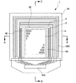
EL表示装置1は、図2に示すように電気絶縁性を備えた基板20と、スイッチング用TFT(図示せず)に接続された画素電極が基板20上にマトリックス状に配置されてなる画素電極域(図示せず)と、画素電極域の周囲に配置されるとともに各画素電極に接続される電源線(図示せず)と、少なくとも画素電極域上に位置する平面視ほぼ矩形の画素部3(図2中一点鎖線枠内)とを具備して構成されたアクティブマトリクス型のものである。
なお、本発明においては、基板20と後述するようにこれの上に形成されるスイッチング用TFTや各種回路、及び層間絶縁膜などを含めて、基体と称している。(図3、4中では符号200で示している。)
Next, a specific configuration of the
As shown in FIG. 2, the
In the present invention, the
画素部3は、中央部分の実表示領域4(図2中二点鎖線枠内)と、実表示領域4の周囲に配置されたダミー領域5(一点鎖線および二点鎖線の間の領域)とに区画される。
実表示領域4には、それぞれ画素電極を有する表示領域R、G、BがA−B方向およびC−D方向にそれぞれ離間してマトリックス状に配置される。
また、実表示領域4の図2中両側には、走査線駆動回路80、80が配置される。これら走査線駆動回路80、80は、ダミー領域5の下側に配置されたものである。
The
In the
Further, scanning
さらに、実表示領域4の図2中上側には、検査回路90が配置される。この検査回路90は、EL表示装置1の作動状況を検査するための回路であって、例えば検査結果を外部に出力する検査情報出力手段(図示せず)を備え、製造途中や出荷時の表示装置の品質、欠陥の検査を行うことができるように構成されたものである。なお、この検査回路90も、ダミー領域5の下側に配置されたものである。
Further, an
走査線駆動回路80および検査回路90は、その駆動電圧が、所定の電源部から駆動電圧導通部310(図3参照)および駆動電圧導通部340(図4参照)を介して、印加されるよう構成される。また、これら走査線駆動回路80および検査回路90への駆動制御信号および駆動電圧は、このEL表示装置1の作動制御を行う所定のメインドライバなどから駆動制御信号導通部320(図3参照)および駆動電圧導通部350(図4参照)を介して、送信および印加される。なお、この場合の駆動制御信号とは、走査線駆動回路80および検査回路90が信号を出力する際の制御に関連するメインドライバなどからの指令信号である。
The scanning
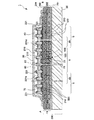
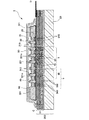
また、EL表示装置1は、図3、図4に示すように基体200上に画素電極23と発光層60と陰極50とを備えた発光素子(有機EL素子)を多数形成し、さらにこれらを覆って緩衝層210、導電層30等を形成させたものである。
なお、発光層60としては、代表的には発光層(エレクトロルミネッセンス層)であり、正孔注入層、正孔輸送層、電子注入層、電子輸送層などのキャリア注入層またはキャリア輸送層を備えるもの。さらには、正孔阻止層(ホールブロッキング層)、電子阻止層(エレクトロン阻止層)を備えるものであってもよい。
In addition, as shown in FIGS. 3 and 4, the
The
基体200を構成する基板20としては、いわゆるトップエミッション型のEL表示装置の場合、この基板20の対向側である導電層30側から発光光を取り出す構成であるので、透明基板及び不透明基板のいずれも用いることができる。不透明基板としては、例えばアルミナ等のセラミックス、ステンレススチール等の金属シートに表面酸化などの絶縁処理を施したもの、また熱硬化性樹脂や熱可塑性樹脂、さらにはそのフィルム(プラスチックフィルム)などが挙げられる。
In the case of a so-called top emission type EL display device, the
また、いわゆるボトムエミッション型のEL表示装置の場合には、基板20側から発光光を取り出す構成であるので、基板20としては、透明あるいは半透明のものが採用される。例えば、ガラス、石英、樹脂(プラスチック、プラスチックフィルム)等が挙げられ、特にガラス基板が好適に用いられる。なお、本実施形態では、導電層30側から発光光を取り出すトップエミッション型とし、よって基板20としては上述した不透明基板、例えば不透明のプラスチックフィルムなどが用いられる。
In the case of a so-called bottom emission type EL display device, since the emitted light is extracted from the
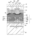
また、基板20上には、画素電極23を駆動するための駆動用TFT123などを含む回路部11が形成されており、その上に発光素子(有機EL素子)が多数設けられる。発光素子は、図5に示すように、陽極として機能する画素電極23と、この画素電極23からの正孔を注入/輸送する正孔輸送層70と、電気光学物質の一つである有機EL物質を備える発光層60と、陰極50とが順に形成されたことによって構成されたものである。
このような構成のもとに、発光素子はその発光層60において、正孔輸送層70から注入された正孔と陰極50からの電子とが結合することにより発光する。
A
Based on such a configuration, the light emitting element emits light by combining holes injected from the
画素電極23は、本実施形態ではトップエミッション型であることから透明である必要がなく、したがって適宜な導電材料によって形成される。
正孔輸送層70の形成材料としては、例えばポリチオフェン誘導体、ポリピロール誘導体など、またはそれらのドーピング体などが用いられる。具体的には、3,4−ポリエチレンジオシチオフェン/ポリスチレンスルフォン酸(PEDOT/PSS)の分散液、すなわち、分散媒としてのポリスチレンスルフォン酸に3,4−ポリエチレンジオシチオフェンを分散させ、さらにこれを水に分散させた分散液などが用いられる。
Since the
As a material for forming the
発光層60を形成するための材料としては、蛍光あるいは燐光を発光することが可能な公知の発光材料を用いることができる。具体的には、(ポリ)フルオレン誘導体(PF)、(ポリ)パラフェニレンビニレン誘導体(PPV)、ポリフェニレン誘導体(PP)、ポリパラフェニレン誘導体(PPP)、ポリビニルカルバゾール(PVK)、ポリチオフェン誘導体、ポリメチルフェニルシラン(PMPS)などのポリシラン系などが好適に用いられる。
また、これらの高分子材料に、ペリレン系色素、クマリン系色素、ローダミン系色素などの高分子系材料や、ルブレン、ペリレン、9,10−ジフェニルアントラセン、テトラフェニルブタジエン、ナイルレッド、クマリン6、キナクリドン等の低分子材料をドープして用いることもできる。
なお、上述した高分子材料に代えて、従来公知の低分子材料を用いることもできる。
また、必要に応じて、このような発光層60の上に電子注入層を形成してもよい。
As a material for forming the
In addition, these polymer materials include polymer materials such as perylene dyes, coumarin dyes, rhodamine dyes, rubrene, perylene, 9,10-diphenylanthracene, tetraphenylbutadiene, Nile red, coumarin 6, and quinacridone. It can also be used by doping a low molecular weight material such as.
In addition, it replaces with the polymeric material mentioned above, a conventionally well-known low molecular material can also be used.
In addition, an electron injection layer may be formed on the
また、本実施形態において正孔輸送層70と発光層60とは、図3〜図5に示すように基体200上にて格子状に形成された親液性制御層25と有機バンク層221とによって囲まれて配置され、これにより囲まれた正孔輸送層70および発光層60は単一の発光素子(有機EL素子)を構成する素子層となる。
なお、有機バンク層221の開口部221aの各壁面の基体200表面に対する角度θが、110度以上から170度以下となっている(図5参照)。このような角度としたのは、発光層60をウエットプロセスにより形成する際に、開口部221a内に配置されやすくするためである。
In the present embodiment, the
Note that the angle θ of each wall surface of the
陰極50は、図3〜図5に示すように、実表示領域4およびダミー領域5の総面積より広い面積を備え、それぞれを覆うように形成されたもので、発光層60と有機バンク層221の上面、さらには有機バンク層221の外側部を形成する壁面を覆った状態で基体200上に形成されたものである。なお、この陰極50は、図4に示すように有機バンク層221の外側で基体200の外周部に形成された陰極用配線202に接続される。この陰極用配線202にはフレキシブル基板203が接続されており、これによって陰極50は、陰極用配線202を介してフレキシブル基板203上の図示しない駆動IC(駆動回路)に接続される。
As shown in FIGS. 3 to 5, the
陰極50を形成するための材料としては、本実施形態はトップエミッション型であることから光透過性である必要があり、したがって透明導電材料が用いられる。透明導電材料としてはITO(Indium Tin Oxide:インジウム錫酸化物)が好適とされるが、これ以外にも、例えば酸化インジウム・酸化亜鉛系アモルファス透明導電膜(Indium Zinc Oxide:IZO/アイ・ゼット・オー)(登録商標)等を用いることができる。アルミニウム、銀、マグネシウムなどの一般的に陰極に用いられる材料を100nm以下の薄膜にて形成して、半透明電極としてもよい。なお、本実施形態ではITOを用いるものとする。
As a material for forming the
陰極50の上層部には、陰極保護層55を形成してもよい。陰極保護層55は、製造プロセス時に陰極50が腐食されてしまうことを防止するために設けられる層であり、無機化合物、例えば、ITO、ICO(酸化インジウムセリウム)、やIZO(登録商標)、珪素化合物により形成される。陰極50を無機化合物からなる陰極保護層55で覆うことにより、無機酸化物からなる陰極50への酸素等の侵入を良好に防止することができる。なお、陰極保護層55は、基板200の外周部の絶縁層284上まで、10nmから300nm程度の厚みに形成される。
A cathode protective layer 55 may be formed on the upper layer portion of the
陰極50の上には、有機バンク層221よりも広い範囲で、かつ陰極50の外側部以外の部位を覆った状態で緩衝層210が設けられる。緩衝層210は、有機バンク層221の形状の影響により、凸凹状に形成された陰極50の凸凹部分を埋めるように配置され、更に、その上面は略平坦に形成される。
緩衝層210は、基板200側から発生する反りや体積変化により発生する応力を緩和し、不安定な有機バンク層221からの陰極50の剥離を防止する機能を有する。また、緩衝層210の上面が略平坦化されるので、緩衝層210上に形成される硬い被膜からなる導電層30も平坦化されるので、応力が集中する部位がなくなり、これにより、導電層30へのクラックの発生を防止する。
緩衝層210としては、親油性で低吸水性を有する高分子材料、例えば、ポリオレフィン系またはポリエーテル系が好ましい。また、メチルトリメトキシシランなどのアルコキシシランを加水分解させて縮合させた有機珪素ポリマーでもよい。更に、シランカップリング剤等の珪素化合物を含んだ高分子を用いることにより、陰極50及び導電層30との界面の接着性を向上させることができる。
なお、緩衝層210における有機バンク層221の上面、すなわち、開口部211a以外の部分には、コンタクトホール212が設けられることが好ましい。コンタクトホール212は、後述する導電層30が成膜されることにより、陰極50と導電層30とが導通するようになるため、陰極50の配線抵抗が低減される。コンタクトホールの開口形状は、円形や楕円形、長方形などの形状で形成される。そして、コンタクトホール212に導電層30が入り込み易くするために、コンタクトホール212の上部側を下部側よりも大きな開口に形成することが望ましい。
A
The
As the
A
更に、このような緩衝層210の上には、緩衝層210の基体200上で露出する部位を覆った状態で導電層30が設けられる。そして、導電層30は、基板200の外周部の絶縁層284上まで形成される。なお、絶縁層284上において、陰極保護層55と接触するようにしてもよい。
導電層30は、導電性を備えるとともに陰極50と連結しているので、陰極50と一体となって電流を流す。これにより、陰極50の導電効率が向上し、陰極50を低抵抗化させる。
また、導電層30は、EL表示装置1の内側に酸素や水分が浸入するのを防止するためガスバリア性を有し、これにより陰極50や発光層60への酸素や水分の浸入を防止し、酸素や水分による陰極50や発光層60の劣化等を抑える。
Further, the
Since the
The
導電層30を形成するための材料としては、本実施形態はトップエミッション型であることから光透過性である必要があり、したがって陰極50と同様に、透明導電材料、例えば、ITO、IZO、ICO(酸化インジウムセリウム)が用いられる。
このように導電層30が金属酸化物で形成されていれば、特に陰極50がITOで形成されることにより、導電層30と陰極50との密着性がよくなり、導電性が向上する。更に、導電層30が欠陥のない緻密な層となって酸素や水分に対するバリア性がより良好になる。
また、このような導電層30の厚さとしては、10nm以上、500nm以下であるのが好ましい。10nm未満であると、膜の欠陥や膜厚のバラツキなどによって部分的に貫通孔が形成されてしまい、ガスバリア性が損なわれてしまうおそれがあるからであり、500nmを越えると、応力による割れが生じてしまうおそれがあるからである。
As a material for forming the
Thus, when the
Further, the thickness of the
更に、導電層30の外側には、導電層30を覆う保護層204が設けられる(図8参照)。この保護層204は、導電層30側に設けられた接着層205と表面保護層206とからなる。
接着層205は、導電層30上に表面保護層206を固定させ、かつ外部からの機械的衝撃に対して緩衝機能を有するもので、例えばウレタン系、アクリル系、エポキシ系、ポリオレフィン系などの樹脂で、後述する表面保護層206より柔軟でガラス転移点の低い材料からなる接着剤によって形成されたものである。なお、このような接着剤には、シランカップリング剤またはアルコキシシランを添加しておくのが好ましく、このようにすれば、形成される接着層205と導電層30との密着性がより良好になり、したがって機械的衝撃に対する緩衝機能が高くなる。
Further, a
The
表面保護層206は、接着層205上に設けられて、保護層204の表面側を構成するものであり、耐圧性や耐摩耗性、外部光反射防止性、ガスバリア性、紫外線遮断性などの機能の少なくとも一つを有してなる層である。具体的には、高分子層(プラスチックフィルム)やDLC(ダイアモンドライクカーボン)層、ガラスなどによって形成されるものである。
なお、この例のEL表示装置においては、トップエミッション型にする場合に表面保護層206、接着層205を共に透光性のものにする必要があるが、ボトムエミッション型とする場合にはその必要はない。
The surface
In the EL display device of this example, when the top emission type is used, both the surface
上述の発光素子の下方には、図5に示したように回路部11が設けられる。この回路部11は、基板20上に形成されて基体200を構成するものである。すなわち、基板20の表面には下地としてSiO2を主体とする下地保護層281が形成され、その上にはシリコン層241が形成される。このシリコン層241の表面には、SiO2および/またはSiNを主体とするゲート絶縁層282が形成される。
A
また、シリコン層241のうち、ゲート絶縁層282を挟んでゲート電極242と重なる領域がチャネル領域241aとされる。なお、このゲート電極242は、図示しない走査線101の一部である。一方、シリコン層241を覆い、ゲート電極242を形成したゲート絶縁層282の表面には、SiO2を主体とする第1層間絶縁層283が形成される。
In addition, a region of the
また、シリコン層241のうち、チャネル領域241aのソース側には、低濃度ソース領域241bおよび高濃度ソース領域241Sが設けられる一方、チャネル領域241aのドレイン側には低濃度ドレイン領域241cおよび高濃度ドレイン領域241Dが設けられて、いわゆるLDD(Light Doped Drain)構造を形成する。これらのうち、高濃度ソース領域241Sは、ゲート絶縁層282と第1層間絶縁層283とにわたって開孔するコンタクトホール243aを介して、ソース電極243に接続される。このソース電極243は、上述した電源線103(図1参照、図5においてはソース電極243の位置に紙面垂直方向に延在する)の一部として構成される。一方、高濃度ドレイン領域241Dは、ゲート絶縁層282と第1層間絶縁層283とにわたって開孔するコンタクトホール244aを介して、ソース電極243と同一層からなるドレイン電極244に接続される。
Further, in the
ソース電極243およびドレイン電極244が形成された第1層間絶縁層283の上層は、例えばアクリル系の樹脂成分を主体とする第2層間絶縁層284によって覆われている。この第2層間絶縁層284は、アクリル系の絶縁膜以外の材料、例えば、SiN、SiO2などを用いることもできる。そして、ITOからなる画素電極23が、この第2層間絶縁層284の表面上に形成されるとともに、第2層間絶縁層284に設けられたコンタクトホール23aを介してドレイン電極244に接続される。すなわち、画素電極23は、ドレイン電極244を介して、シリコン層241の高濃度ドレイン領域241Dに接続される。
The upper layer of the first
なお、走査線駆動回路80および検査回路90に含まれるTFT(駆動回路用TFT)、すなわち、例えばこれらの駆動回路のうち、シフトレジスタに含まれるインバータを構成するNチャネル型又はPチャネル型のTFTは、画素電極23と接続されていない点を除いて駆動用TFT123と同様の構造とされる。
Note that TFTs (driving circuit TFTs) included in the scanning
画素電極23が形成された第2層間絶縁層284の表面には、画素電極23と、上述した親液性制御層25及び有機バンク層221とが設けられる。親液性制御層25は、例えばSiO2などの親液性材料を主体とするものであり、有機バンク層221は、アクリルやポリイミドなどからなるものである。そして、画素電極23の上には、親液性制御層25に設けられた開口部25a、および有機バンク層221に囲まれてなる開口部221aの内部に、正孔輸送層70と発光層60とがこの順に積層される。なお、本実施形態における親液性制御層25の「親液性」とは、少なくとも有機バンク層221を構成するアクリル、ポリイミドなどの材料と比べて親液性が高いことを意味するものとする。
以上に説明した基板20上の第2層間絶縁層284までの層が、回路部11を構成する。
On the surface of the second
The layers up to the second
ここで、本実施形態のEL表示装置1は、カラー表示を行うべく、各発光層60が、その発光波長帯域が光の三原色にそれぞれ対応して形成される。例えば、発光層60として、発光波長帯域が赤色に対応した赤色用発光層60R、緑色に対応した緑色用発光層60G、青色に対応した青色用有機EL層60Bとをそれぞれに対応する表示領域R、G、Bに設け、これら表示領域R、G、Bをもってカラー表示を行う1画素が構成される。また、各色表示領域の境界には、金属クロムをスパッタリングなどにて成膜した図示略のBM(ブラックマトリクス)が、例えば有機バンク層221と親液性制御層25との間に形成される。
Here, in the
次に、本実施形態に係るEL表示装置1の製造方法の一例を、図6,7を参照して説明する。図6,7に示す各断面図は、図2中のA−B線の断面図に対応した図である。
なお、本実施形態においては、電気光学装置としてのEL表示装置1がトップエミッション型である場合であり、また、基板20の表面に回路部11を形成させる工程については、従来技術と変わらないので説明を省略する。
Next, an example of a method for manufacturing the
In this embodiment, the
まず、図6(a)に示すように、表面に回路部11が形成された基板20の全面を覆うように、画素電極23となる導電膜を形成され、更に、この透明導電膜をパターニングすることにより、第2層間絶縁層284のコンタクトホール23aを介してドレイン電極244と導通する画素電極23を形成すると同時に、ダミー領域のダミーパターン26も形成する。
なお、図3、4では、これら画素電極23、ダミーパターン26を総称して画素電極23としている。ダミーパターン26は、第2層間絶縁層284を介して下層のメタル配線へ接続しない構成とされる。すなわち、ダミーパターン26は、島状に配置され、実表示領域に形成されている画素電極23の形状とほぼ同一の形状を有する。もちろん、表示領域に形成されている画素電極23の形状と異なる構造であってもよい。なお、この場合、ダミーパターン26は少なくとも駆動電圧導通部310(340)の上方に位置するものも含むものとする。
First, as shown in FIG. 6A, a conductive film to be the
3 and 4, the
次いで、図6(b)に示すように、画素電極23、ダミーパターン26上、および第2層間絶縁膜上に絶縁層である親液性制御層25を形成する。なお、画素電極23においては一部が開口する態様にて親液性制御層25を形成し、開口部25a(図3も参照)において画素電極23からの正孔移動が可能とされている。逆に、開口部25aを設けないダミーパターン26においては、絶縁層(親液性制御層)25が正孔移動遮蔽層となって正孔移動が生じないものとされている。続いて、親液性制御層25において、異なる2つの画素電極23の間に位置して形成された凹状部に不図示のBM(ブラックマトリックス)を形成する。具体的には、親液性制御層25の凹状部に対して、金属クロムを用いスパッタリング法にて成膜する。
Next, as shown in FIG. 6B, a
そして、図6(c)に示すように、親液性制御層25の所定位置、詳しくは上述したBMを覆うように有機バンク層221を形成する。具体的な有機バンク層の形成方法としては、例えばアクリル樹脂、ポリイミド樹脂などのレジストを溶媒に溶解したものを、スピンコート法、ディップコート法などの各種塗布法により塗布して有機質層を形成する。なお、有機質層の構成材料は、後述するインクの溶媒に溶解せず、しかもエッチングなどによってパターニングし易いものであればどのようなものでもよい。
Then, as shown in FIG. 6C, an
更に、有機質層をフォトリソグラフィ技術、エッチング技術を用いてパターニングし、有機質層に開口部221aを形成することにより、開口部221aに壁面を有した有機バンク層221を形成する。ここで、開口部221を形成する壁面について、基体200表面に対する角度θを110度以上から170度以下となるように形成する。
なお、この場合、有機バンク層221は、少なくとも駆動制御信号導通部320の上方に位置するものを含むものとする。
Further, the organic layer is patterned using a photolithography technique and an etching technique to form an
In this case, the
次いで、有機バンク層221の表面に、親液性を示す領域と、撥液性を示す領域とを形成する。本実施形態においては、プラズマ処理によって各領域を形成する。具体的には、プラズマ処理を、予備加熱工程と、有機バンク層221の上面および開口部221aの壁面ならびに画素電極23の電極面23c、親液性制御層25の上面をそれぞれ親液性にする親インク化工程と、有機バンク層221の上面および開口部221aの壁面を撥液性にする撥インク化工程と、冷却工程とで構成する。
Next, a region showing lyophilicity and a region showing liquid repellency are formed on the surface of the
すなわち、基材(バンクなどを含む基板20)を所定温度、例えば70〜80℃程度に加熱し、次いで親インク化工程として大気雰囲気中で酸素を反応ガスとするプラズマ処理(O2プラズマ処理)を行う。次いで、撥インク化工程として大気雰囲気中で4フッ化メタンを反応ガスとするプラズマ処理(CF4プラズマ処理)を行い、その後、プラズマ処理のために加熱された基材を室温まで冷却することで、親液性および撥液性が所定箇所に付与されることとなる。
That is, a base material (
なお、このCF4プラズマ処理においては、画素電極23の電極面23cおよび親液性制御層25についても多少の影響を受けるが、画素電極23の材料であるITOおよび親液性制御層25の構成材料であるSiO2、TiO2などはフッ素に対する親和性に乏しいため、親インク化工程で付与された水酸基がフッ素基で置換されることがなく、親液性が保たれる。
In this CF 4 plasma treatment, the electrode surface 23c of the
次いで、正孔輸送層形成工程によって正孔輸送層70の形成を行う。この正孔輸送層形成工程では、例えばインクジェット法等の液滴吐出法や、スピンコート法などにより、正孔輸送層材料を電極面23c上に塗布し、その後、乾燥処理および熱処理を行い、電極23上に正孔輸送層70を形成する。正孔輸送層材料を例えばインクジェット法で選択的に塗布する場合には、まず、インクジェットヘッド(図示略)に正孔輸送層材料を充填し、インクジェットヘッドの吐出ノズルを親液性制御層25に形成された開口部25a内に位置する電極面23cに対向させ、インクジェットヘッドと基材(基板20)とを相対移動させながら、吐出ノズルから1滴当たりの液量が制御された液滴を電極面23cに吐出する。次に、吐出後の液滴を乾燥処理し、正孔輸送層材料に含まれる分散媒や溶媒を蒸発させることにより、正孔輸送層70を形成する。
Next, the
ここで、吐出ノズルから吐出された液滴は、親液性処理がなされた電極面23c上にて広がり、親液性制御層25の開口部25a内に満たされる。その一方で、撥インク処理された有機バンク層221の上面では、液滴がはじかれて付着しない。したがって、液滴が所定の吐出位置からはずれて有機バンク層221の上面に吐出されたとしても、該上面が液滴で濡れることがなく、弾かれた液滴が親液性制御層25の開口部25a内に転がり込む。
なお、この正孔輸送層形成工程以降は、正孔輸送層70および発光層60の酸化を防止すべく、窒素雰囲気、アルゴン雰囲気などの不活性ガス雰囲気で行うのが好ましい。
Here, the droplets ejected from the ejection nozzle spread on the electrode surface 23c that has been subjected to the lyophilic treatment, and are filled in the
In addition, after this hole transport layer formation process, in order to prevent the oxidation of the
次いで、発光層形成工程によって発光層60の形成を行う。この発光層形成工程では、例えばインクジェット法により、発光層形成材料を正孔輸送層70上に吐出し、その後、乾燥処理および熱処理を行うことにより、有機バンク層221に形成された開口部221a内に発光層60を形成する。この発光層形成工程では、正孔輸送層70の再溶解を防止するため、発光層形成材料に用いる溶媒として、正孔輸送層70に対して不溶な無極性溶媒を用いる。
なお、この発光層形成工程では、インクジェット法によって例えば青色(B)の発光層形成材料を青色の表示領域に選択的に塗布し、乾燥処理した後、同様にして緑色(G)、赤色(R)についてもそれぞれその表示領域に選択的に塗布し、乾燥処理する。
また、必要に応じて、上述したようにこのような発光層60の上に電子注入層を形成してもよい。
Next, the
In this light emitting layer forming step, for example, a blue (B) light emitting layer forming material is selectively applied to a blue display region by an inkjet method, dried, and then similarly treated with green (G) and red (R ) Is also selectively applied to the display area and dried.
If necessary, an electron injection layer may be formed on the
次いで、図7(d)に示すように、陰極層形成工程によって陰極50の形成を行う。この陰極層形成工程では、例えば蒸着法等の物理的気相蒸着法によりITOを成膜して、陰極50とする。このとき、この陰極50については、発光層60と有機バンク層221の上面を覆うのはもちろん、有機バンク層221の外側部を形成する壁面についてもこれを覆った状態となるように形成する。
なお、陰極50上に陰極保護層55を形成させる場合には、蒸着法等の物理的気相蒸着法によりシリコン酸化物等を陰極50上に成膜させる。
Next, as shown in FIG. 7D, the
When the cathode protective layer 55 is formed on the
次いで、図7(e)に示すように、緩衝層210は、塗布方式、すなわちウエットプロセスにより形成する。例えばインクジェット法で形成する場合には、まず、インクジェットヘッド(図示略)に緩衝層材料を充填し、インクジェットヘッドの吐出ノズルを陰極50に対向させ、インクジェットヘッドと基材(基板20)とを相対移動させながら、吐出ノズルから1滴当たりの液量が制御された液滴を陰極50に吐出する。次に、吐出後の液滴を乾燥処理し、緩衝層材料に含まれる分散媒や溶媒を蒸発させることにより、緩衝層210を形成する。
また、スリットコート(或いはカーテンコート)法により、緩衝層材料を塗布してもよい。また、緩衝層210と同時にコンタクトホール212を形成するために、緩衝層210をスクリーン印刷法により形成してもよい。更に、形成後の緩衝層210にフォトレジストを塗布して、コンタクトホール212を形成してもよい。
Next, as shown in FIG. 7E, the
Further, the buffer layer material may be applied by a slit coat (or curtain coat) method. Further, in order to form the
次いで、図7(g)に示すように、陰極50及び緩衝層210を覆って、すなわち基体200上にて露出する陰極50の全ての部位を覆った状態に導電層30を形成する。これにより、陰極50の外周部及びコンタクトホール212部分において、陰極50と導電層30とが接続する。
ここで、この導電層30の形成方法としては、先にスパッタリング法やイオンプレーティング法等の物理的気相蒸着法で成膜を行い、次いで、プラズマCVD法等の化学的気相蒸着法で成膜を行うのが好ましい。スパッタリング法やイオンプレーティング法等の物理的気相蒸着法は、一般に異質な基板表面に対しても比較的密着性の良い膜が得られるものの、得られる膜に関しては粒塊状で欠陥が発生しやすく、また応力の大きい被膜になりやすいなどの欠点がある。一方、化学的気相蒸着法では、応力が少なくステップカバーレッジ性に優れた欠陥が少なく緻密で良好な膜質のものが得られるものの、一般に異質な基板表面に対する密着性や造膜性が得られにくいといった欠点がある。そこで、初期の成膜については物理的気相蒸着法を採用して例えば必要な膜厚の半分あるいはそれ以上を形成し、後期の成膜において化学的気相蒸着法を用いることにより、先に形成した膜の欠陥を補うようにすれば、全体としてガスバリア性(酸素や水分に対するバリア性)に優れた導電層30を比較的短時間で形成することができる。
Next, as shown in FIG. 7G, the
Here, as a method for forming the
また、導電層30の形成については、同一の材料によって単層で形成してもよく、また異なる材料で複数の層に積層して形成してもよく、さらには、単層で形成するものの、その組成を膜厚方向で連続的あるいは非連続的に変化させるようにして形成してもよい。
異なる材料で複数の層に積層して形成する場合、例えば、上述したように物理的気相蒸着法で形成する内側の層(陰極50側の層)を金属酸化物とし、化学的気相蒸着法で形成する外側の層を珪素酸窒化物や珪素酸化物などとするのが好ましい。
In addition, the
When a plurality of layers are stacked with different materials, for example, as described above, the inner layer (layer on the
更に、物理的気相蒸着法で内側の層を形成する際、成膜装置内に供給する酸素量を最初は少なくし、以下、連続的あるいは非連続的に増やすことにより、形成する導電層30中の酸素濃度を陰極50側(内側)で低くし、外側ではこれより高くなるように形成してもよい。
なお、導電層30の形成については単一の成膜法で行ってもよいのはもちろんであり、その場合にも、上述したように酸素濃度を陰極50側(内側)で低くなるように形成するのが好ましい。
Furthermore, when the inner layer is formed by physical vapor deposition, the amount of oxygen supplied into the film forming apparatus is initially reduced, and thereafter, the
The
そして、図8に示すように、導電層30上に接着層205と表面保護層206からなる保護層204が設けられる。接着層205は、スリットコート法などにより導電層30上に略均一に塗布され、その上に表面保護層206が貼り合わされる。
このように導電層30上に保護層204を設ければ、表面保護層206が耐圧性や耐摩耗性、光反射防止性、ガスバリア性、紫外線遮断性などの機能を有していることにより、発光層60や陰極50、さらにはガスバリア層もこの表面保護層206によって保護することができ、したがって発光素子の長寿命化を図ることができる。
また、接着層205が機械的衝撃に対して緩衝機能を発揮するので、外部から機械的衝撃が加わった場合に、導電層30やこの内側の発光素子への機械的衝撃を緩和し、この機械的衝撃による発光素子の機能劣化を防止することができる。
Then, as shown in FIG. 8, a
When the
Further, since the
以上のようにして、EL表示装置1が形成される。
このようなEL表示装置1にあっては、陰極50と導電層30との間に、陰極50を覆うとともに略平坦な上面が形成された緩衝層210が配置されるので、緩衝層210が基板200側から発生する反りや体積変化により発生する応力を緩和し、不安定な有機バンク層221からの陰極50の剥離を防止することができる。
更に、緩衝層210の上面が略平坦化されているので、緩衝層210上に形成される硬い被膜からなる導電層30が平坦化されるので、導電層30に応力が集中する部位がなくなり、これにより、導電層30へのクラックの発生を防止できる。
また、導電層30が陰極50と導通するので、陰極50を低抵抗化することができ、消費電力を低減させるとともに、発熱を抑えることができる。
As described above, the
In such an
Furthermore, since the upper surface of the
Further, since the
なお、上述した実施形態では、トップエミッション型のEL表示装置1を例にして説明したが、本発明はこれに限定されることなく、ボトムエミッション型にも、また、両側に発光光を出射するタイプのものにも適用可能である。
In the above-described embodiment, the top emission type
また、ボトムエミッション型、あるいは両側に発光光を出射するタイプのものとした場合、基体200に形成するスイッチング用TFT112や駆動用TFT123については、発光素子の直下ではなく、親液性制御層25および有機バンク層221の直下に形成するようにし、開口率を高めるのが好ましい。
また、EL表示装置1では本発明における第1の電極を陽極として機能させ、第2の電極を陰極として機能させたが、これらを逆にして第1の電極を陰極、第2の電極を陽極としてそれぞれ機能させるよう構成してもよい。ただし、その場合には、発光層60と正孔輸送層70との形成位置を入れ替えるようにする必要がある。
Further, in the case of a bottom emission type or a type that emits emitted light on both sides, the switching
In the
また、本実施形態では、電気光学装置にEL表示装置1を適用した例を示したが、本発明はこれに限定されることなく、基本的に第2電極が基体の外側に設けられるものであれば、どのような形態の電気光学装置にも適用可能である。
In this embodiment, the
次に、本発明の電子機器について説明する。電子機器は、上述したEL表示装置(電気光学装置)1を表示部として有したものであり、具体的には図9に示すものが挙げられる。
図9(a)は、携帯電話の一例を示した斜視図である。図9(a)において、携帯電話1000は、上述したEL表示装置1を用いた表示部1001を備える。
図9(b)は、腕時計型電子機器の一例を示した斜視図である。図9(b)において、時計1100は、上述したEL表示装置1を用いた表示部1101を備える。
図9(c)は、ワープロ、パソコンなどの携帯型情報処理装置の一例を示した斜視図である。図9(c)において、情報処理装置1200は、キーボードなどの入力部1201、上述したEL表示装置1を用いた表示部1202、情報処理装置本体(筐体)1203を備える。
図9(a)〜(c)に示すそれぞれの電子機器は、上述したEL表示装置(電気光学装置)1を有した表示部1001,1101,1202を備えているので、表示部を構成するEL表示装置の発光素子の長寿命化が図られたものとなる。
Next, the electronic apparatus of the present invention will be described. The electronic apparatus has the above-described EL display device (electro-optical device) 1 as a display unit, and specifically, the one shown in FIG.
FIG. 9A is a perspective view showing an example of a mobile phone. In FIG. 9A, a
FIG. 9B is a perspective view illustrating an example of a wristwatch type electronic device. In FIG. 9B, a
FIG. 9C is a perspective view showing an example of a portable information processing apparatus such as a word processor or a personal computer. In FIG. 9C, the
Each of the electronic devices shown in FIGS. 9A to 9C includes the
1 表示装置(電気光学装置)、 23 画素電極(第1電極)、 30 導電層、 50 陰極(第2電極)、 55 陰極保護層(保護層)、 60 発光層(電気光学層)、 200 基体、 210 緩衝層、 221 有機バンク層(バンク構造体)、 221a 開口部、 1000 携帯電話(電子機器)、1100 時計(電子機器)、 1200 情報処理装置(電子機器)、 1001,1101,1202 表示部(電気光学装置)
DESCRIPTION OF
Claims (17)
複数の第1電極と、
前記第1電極の形成位置に対応した複数の開口部を有するバンク層と、
前記開口部のそれぞれに配置される電気光学層と、
前記バンク層及び前記電気光学層を覆う第2電極と、
前記第2電極の上に積層され、略平坦な上面が形成された緩衝層と、
前記緩衝層を覆うとともに前記第2電極と導通する導電層と、を有し、
前記導電層は、前記第2電極および前記緩衝層を覆い、かつ前記第2電極の外側まで延在して前記第2電極の外側において前記基体と接していることを特徴とする電気光学装置。 On the substrate,
A plurality of first electrodes;
A bank layer having a plurality of openings corresponding to the formation position of the first electrode;
An electro-optic layer disposed in each of the openings;
A second electrode covering the bank layer and the electro-optic layer;
A buffer layer laminated on the second electrode and having a substantially flat upper surface;
A conductive layer that covers the buffer layer and is electrically connected to the second electrode ;
The electro-optical device , wherein the conductive layer covers the second electrode and the buffer layer, extends to the outside of the second electrode, and is in contact with the base on the outside of the second electrode .
前記第2電極用配線は、前記バンク層の外側で前記第2電極と接続されていることを特徴とする請求項1乃至3のいずれかに記載の電気光学装置。 4. The electro-optical device according to claim 1, wherein the second electrode wiring is connected to the second electrode outside the bank layer. 5.
前記導電層と前記保護層との間には、前記導電層と前記保護層とを接着する接着層が設けられていることを特徴とする請求項1乃至5のいずれかに記載の電気光学装置。 6. The electro-optical device according to claim 1, wherein an adhesive layer that bonds the conductive layer and the protective layer is provided between the conductive layer and the protective layer. .
ウエットプロセスにより前記第2電極上に緩衝層を配置するとともに略平坦な上面を形成する工程と、
前記緩衝層上に前記第2電極と導通する導電層を、前記第2電極および前記緩衝層の全面を覆い、かつ前記第2電極の外側まで延在して前記第2電極の外側において前記基体と接するように形成する工程と、を有することを特徴とする電気光学装置の製造方法。 On the substrate, a plurality of first electrodes, a bank layer having a plurality of openings corresponding to the positions where the first electrodes are formed, an electro-optic layer disposed in each of the openings, the bank layer, and the bank layer In a method for manufacturing an electro-optical device having a second electrode covering the electro-optical layer,
Disposing a buffer layer on the second electrode by a wet process and forming a substantially flat upper surface;
A conductive layer electrically connected to the second electrode on the buffer layer; covers the entire surface of the second electrode and the buffer layer; and extends to the outside of the second electrode so as to be outside the second electrode. And a method of manufacturing the electro-optical device.
Priority Applications (1)
| Application Number | Priority Date | Filing Date | Title |
|---|---|---|---|
| JP2003312762A JP4428005B2 (en) | 2003-09-04 | 2003-09-04 | Electro-optical device, method of manufacturing electro-optical device, and electronic apparatus |
Applications Claiming Priority (1)
| Application Number | Priority Date | Filing Date | Title |
|---|---|---|---|
| JP2003312762A JP4428005B2 (en) | 2003-09-04 | 2003-09-04 | Electro-optical device, method of manufacturing electro-optical device, and electronic apparatus |
Publications (3)
| Publication Number | Publication Date |
|---|---|
| JP2005085487A JP2005085487A (en) | 2005-03-31 |
| JP2005085487A5 JP2005085487A5 (en) | 2008-11-06 |
| JP4428005B2 true JP4428005B2 (en) | 2010-03-10 |
Family
ID=34413924
Family Applications (1)
| Application Number | Title | Priority Date | Filing Date |
|---|---|---|---|
| JP2003312762A Expired - Fee Related JP4428005B2 (en) | 2003-09-04 | 2003-09-04 | Electro-optical device, method of manufacturing electro-optical device, and electronic apparatus |
Country Status (1)
| Country | Link |
|---|---|
| JP (1) | JP4428005B2 (en) |
Families Citing this family (7)
| Publication number | Priority date | Publication date | Assignee | Title |
|---|---|---|---|---|
| JP4555727B2 (en) * | 2005-04-22 | 2010-10-06 | 株式会社 日立ディスプレイズ | Organic light emitting display |
| JP5214440B2 (en) * | 2005-05-23 | 2013-06-19 | トムソン ライセンシング | Luminescent panel for illumination or image display with composite transparent upper electrode |
| JP2007227288A (en) * | 2006-02-27 | 2007-09-06 | Seiko Epson Corp | Organic el device and electronic equipment |
| JP6111461B2 (en) * | 2013-10-23 | 2017-04-12 | 株式会社Joled | Display device and electronic device |
| KR102491880B1 (en) * | 2016-06-16 | 2023-01-27 | 삼성디스플레이 주식회사 | Organic light emitting display and manufacturing method thereof |
| CN111149431B (en) * | 2017-09-28 | 2022-08-09 | 夏普株式会社 | Display device and method of manufacturing display device |
| JP7081628B2 (en) * | 2020-08-06 | 2022-06-07 | セイコーエプソン株式会社 | Luminous device and electronic device |
-
2003
- 2003-09-04 JP JP2003312762A patent/JP4428005B2/en not_active Expired - Fee Related
Also Published As
| Publication number | Publication date |
|---|---|
| JP2005085487A (en) | 2005-03-31 |
Similar Documents
| Publication | Publication Date | Title |
|---|---|---|
| JP4561201B2 (en) | Electro-optical device, method of manufacturing electro-optical device, and electronic apparatus | |
| JP3997888B2 (en) | Electro-optical device, method of manufacturing electro-optical device, and electronic apparatus | |
| KR100638160B1 (en) | Method for manufacturing electro-optic device, electro-optic device, and electronic apparatus | |
| JP4539547B2 (en) | LIGHT EMITTING DEVICE, LIGHT EMITTING DEVICE MANUFACTURING METHOD, AND ELECTRONIC DEVICE | |
| JP4138672B2 (en) | Manufacturing method of electro-optical device | |
| JP4479381B2 (en) | Electro-optical device, method of manufacturing electro-optical device, and electronic apparatus | |
| KR100682815B1 (en) | Light-emitting device, method of manufacturing the same, and electronic apparatus | |
| JP4631683B2 (en) | Light emitting device and electronic device | |
| JP4792717B2 (en) | Electro-optical device, method of manufacturing electro-optical device, and electronic apparatus | |
| JP2008218423A (en) | Electro-optical device, and electronic apparatus | |
| JP4465951B2 (en) | Manufacturing method of electro-optical device | |
| JP4678124B2 (en) | Electro-optical device, method of manufacturing electro-optical device, and electronic apparatus | |
| JP2004127606A (en) | Electrooptical device and electronic apparatus | |
| JP4470421B2 (en) | Manufacturing method of electro-optical device | |
| JP4701580B2 (en) | ELECTRO-OPTICAL DEVICE, ITS MANUFACTURING METHOD, AND ELECTRONIC DEVICE | |
| JP4428005B2 (en) | Electro-optical device, method of manufacturing electro-optical device, and electronic apparatus | |
| JP4552390B2 (en) | Manufacturing method of organic EL device | |
| JP4736544B2 (en) | Electro-optical device and electronic apparatus | |
| JP2004303671A (en) | Manufacturing method of electro-optical device, electro-optical device, and electronic equipment | |
| JP4613700B2 (en) | Electro-optical device and electronic apparatus | |
| JP2009283149A (en) | Method of manufacturing electro-optical device as well as electro-optical device and electronic equipment | |
| JP5003808B2 (en) | Electro-optical device and electronic apparatus | |
| JP4466479B2 (en) | Electro-optical device and electronic apparatus | |
| JP2009187962A (en) | Electro-optical device, and electronic apparatus | |
| JP2007242998A (en) | Light-emitting device, method of manufacturing the same, and electronic equipment |
Legal Events
| Date | Code | Title | Description |
|---|---|---|---|
| A621 | Written request for application examination |
Free format text: JAPANESE INTERMEDIATE CODE: A621 Effective date: 20060614 |
|
| RD04 | Notification of resignation of power of attorney |
Free format text: JAPANESE INTERMEDIATE CODE: A7424 Effective date: 20070403 |
|
| A521 | Request for written amendment filed |
Free format text: JAPANESE INTERMEDIATE CODE: A523 Effective date: 20080919 |
|
| A977 | Report on retrieval |
Free format text: JAPANESE INTERMEDIATE CODE: A971007 Effective date: 20090520 |
|
| A131 | Notification of reasons for refusal |
Free format text: JAPANESE INTERMEDIATE CODE: A131 Effective date: 20090526 |
|
| A521 | Request for written amendment filed |
Free format text: JAPANESE INTERMEDIATE CODE: A523 Effective date: 20090724 |
|
| TRDD | Decision of grant or rejection written | ||
| A01 | Written decision to grant a patent or to grant a registration (utility model) |
Free format text: JAPANESE INTERMEDIATE CODE: A01 Effective date: 20091124 |
|
| A01 | Written decision to grant a patent or to grant a registration (utility model) |
Free format text: JAPANESE INTERMEDIATE CODE: A01 |
|
| FPAY | Renewal fee payment (event date is renewal date of database) |
Free format text: PAYMENT UNTIL: 20121225 Year of fee payment: 3 |
|
| R150 | Certificate of patent or registration of utility model |
Free format text: JAPANESE INTERMEDIATE CODE: R150 Ref document number: 4428005 Country of ref document: JP Free format text: JAPANESE INTERMEDIATE CODE: R150 |
|
| A61 | First payment of annual fees (during grant procedure) |
Free format text: JAPANESE INTERMEDIATE CODE: A61 Effective date: 20091207 |
|
| FPAY | Renewal fee payment (event date is renewal date of database) |
Free format text: PAYMENT UNTIL: 20121225 Year of fee payment: 3 |
|
| FPAY | Renewal fee payment (event date is renewal date of database) |
Free format text: PAYMENT UNTIL: 20131225 Year of fee payment: 4 |
|
| S531 | Written request for registration of change of domicile |
Free format text: JAPANESE INTERMEDIATE CODE: R313531 |
|
| R350 | Written notification of registration of transfer |
Free format text: JAPANESE INTERMEDIATE CODE: R350 |
|
| LAPS | Cancellation because of no payment of annual fees |