JP4424760B2 - Emulation system using time-multiplexed interconnection - Google Patents
Emulation system using time-multiplexed interconnection Download PDFInfo
- Publication number
- JP4424760B2 JP4424760B2 JP50074799A JP50074799A JP4424760B2 JP 4424760 B2 JP4424760 B2 JP 4424760B2 JP 50074799 A JP50074799 A JP 50074799A JP 50074799 A JP50074799 A JP 50074799A JP 4424760 B2 JP4424760 B2 JP 4424760B2
- Authority
- JP
- Japan
- Prior art keywords
- logic
- emulation system
- signal
- chip
- input
- Prior art date
- Legal status (The legal status is an assumption and is not a legal conclusion. Google has not performed a legal analysis and makes no representation as to the accuracy of the status listed.)
- Expired - Fee Related
Links
Images


Classifications
-
- G—PHYSICS
- G01—MEASURING; TESTING
- G01R—MEASURING ELECTRIC VARIABLES; MEASURING MAGNETIC VARIABLES
- G01R31/00—Arrangements for testing electric properties; Arrangements for locating electric faults; Arrangements for electrical testing characterised by what is being tested not provided for elsewhere
- G01R31/28—Testing of electronic circuits, e.g. by signal tracer
- G01R31/2851—Testing of integrated circuits [IC]
- G01R31/2853—Electrical testing of internal connections or -isolation, e.g. latch-up or chip-to-lead connections
-
- G—PHYSICS
- G01—MEASURING; TESTING
- G01R—MEASURING ELECTRIC VARIABLES; MEASURING MAGNETIC VARIABLES
- G01R31/00—Arrangements for testing electric properties; Arrangements for locating electric faults; Arrangements for electrical testing characterised by what is being tested not provided for elsewhere
- G01R31/28—Testing of electronic circuits, e.g. by signal tracer
- G01R31/317—Testing of digital circuits
- G01R31/31712—Input or output aspects
- G01R31/31717—Interconnect testing
-
- G—PHYSICS
- G06—COMPUTING; CALCULATING OR COUNTING
- G06F—ELECTRIC DIGITAL DATA PROCESSING
- G06F30/00—Computer-aided design [CAD]
- G06F30/30—Circuit design
- G06F30/32—Circuit design at the digital level
- G06F30/33—Design verification, e.g. functional simulation or model checking
- G06F30/3308—Design verification, e.g. functional simulation or model checking using simulation
- G06F30/331—Design verification, e.g. functional simulation or model checking using simulation with hardware acceleration, e.g. by using field programmable gate array [FPGA] or emulation
-
- Y—GENERAL TAGGING OF NEW TECHNOLOGICAL DEVELOPMENTS; GENERAL TAGGING OF CROSS-SECTIONAL TECHNOLOGIES SPANNING OVER SEVERAL SECTIONS OF THE IPC; TECHNICAL SUBJECTS COVERED BY FORMER USPC CROSS-REFERENCE ART COLLECTIONS [XRACs] AND DIGESTS
- Y10—TECHNICAL SUBJECTS COVERED BY FORMER USPC
- Y10S—TECHNICAL SUBJECTS COVERED BY FORMER USPC CROSS-REFERENCE ART COLLECTIONS [XRACs] AND DIGESTS
- Y10S370/00—Multiplex communications
- Y10S370/916—Multiplexer/demultiplexer
Abstract
Description
発明の技術分野
本発明は、一般的には電子回路設計を検証するための装置に関し、より詳細には複数の設計信号がプログラム可能なロジック・チップ(logic chip)間で1つの物理的な結線により伝送されるハードウェア・エミュレーション・システム(hardware emulation system)に関する。
発明の背景技術
ハードウェア・エミュレーション・システムは、チップ又はプリント回路基板の製造に先立って電子回路設計を検証するために設計された装置である。これらのシステムは、一般的には、プログラム可能なロジック・チップ(ロジック・チップ)及びプログラム可能な相互接続チップ(相互接続チップ)(interconnectchip)によって構築される。ここで、「チップ」という用語は、集積回路をいうものとする。ロジック・チップの例としては、フィールド・プログラマブル・ゲート・アレイ(field-programmable gate arrays)(“FPGAs”)のような再プログラム可能な論理回路(logic circuit)を含み、既製品と注文品が含まれる。相互接続チップの例としては、再プログラム可能なFPGA、マルチプレクサ・チップ(multiplexer chip)、クロスポイント・スイッチ・チップ(crosspoint switch chip)等を含む。相互接続チップは、既製品又は注文設計された製品のいずれであってもよい。
従来のエミュレーション・システムは、一般的に、エミュレーションされる1つの電子回路設計内の各信号が1つのロジック・チップ内の1つ又は複数の物理的な金属配線(“ワイヤ”)にマップされるように設計されていた。ロジック・チップ間でやりとりされる信号は、1つのロジック・チップ上の1つ又は複数の物理的ピンと、ロジック・チップ及び相互接続チップを含むプリント回路基板上の1つ若しくは複数の物理的な経路にマップされていた。
従来のエミュレーション・システムにおける設計信号の物理的なピン及び経路に対する1対1のマッピングのため、エミュレーション・システムは、少なくともロジック・チップの間を接続する設計信号と同じ数のロジック・チップのピン及びプリント回路基板の経路が必要である。このような構成によれば、エミュレーション・システムを構成するために、非常に複雑で高価な集積回路のパッケージ、プリント回路基板及び回路基板コネクタが必要であった。これらの部品は高価であるために、ハードウェア・ロジック・エミュレーション・システムの価格も順次高価なものとなり、設計者の数が限定され、それにより、システムからの恩恵が限定され、ハードウェア・エミュレーション・システムの優位性が限定される要因となっていた。
さらに、集積回路の製造技術の進展により、急速に小型化されたサイズのものが使用できるようになった。このため、ロジック・チップのロジック密度(すなわち、ロジック・チップの中に設けることができるロジック・ゲートの数)は劇的に増加した。しかしながら、1つのロジック・チップに設けられ又はエミュレートされるロジック・ゲートの数の増加は、チップのパッケージ(package)の入力、出力、クロック等に利用可能なピン(すなわち、リード線)の数の増加に結びつかない。集積回路パッケージのピンの数は、チップの利用可能な周辺の長さにより限定される。さらに、集積回路のダイス(dice)上の結合パッドをパッケージ上のピンに接続するために用いられるワイヤ・ボンディング組み立て装置の能力は、長い時間をかけてゆっくりと向上している。このため、1つのロジック・チップ上で利用可能なロジックの数と、これらのロジックを外部に接続するために利用可能なピンの数との間の食い違いは、ますます大きなものとなっている。このため、ロジック・チップの論理的な容量(logical capacity)の平均的な利用率は低く、任意の大きさの電子回路設計のエミュレーションに必要とされるハードウェア・エミュレーション・システムのコストを押し上げる結果となっている。
時間多重(time-multiplexing)は、各物理的な接続のコストが非常に高いあるタイプのシステムにおいて、複数の論理信号の間で1つの物理的ワイヤ又はピンを共有するために用いられてきた技術である。このようなシステムには、遠距離通信システムが含まれる。しかしながら、従来の時間多重技術方法ではエミュレートされる回路の動作速度が大きく低下するため、時間多重は、Quickturn Design Systems,Inc.、Mentor Graphics Corporation、Aptix Corporationその他により提供されるハードウェア・エミュレーション・システムには一般的には用いられていなかった。さらに、従来の時間多重技術では、ハードウェア・エミュレーション・システムにおいて、組み込みまれた設計の非同期の動作を正しく保持することが困難である。
前述したように、ハードウェア・エミュレーション・システムの1つの機能は、集積回路の機能を検証することにある。典型的には、回路の設計者又は技術者が集積回路を設計する時、その設計は、設計の“ネットリスト”記述の形で表わされる。ネットリスト記述(又は当業者によって呼ばれている“ネットリスト”)は、集積回路の部品及びその部品の間の電気的な相互接続を記述したものである。これらの部品には、ロジック回路を供給するために必要なすべての回路要素(例えば、ゲート)及びシーケンシャル・ロジック(sequential logic)(例えば、フリップ・フロップ及びラッチ)が含まれる。従来のエミュレーション・システムでは、ネットリストをハードウェア・エミュレーション・システムに供給する前に、ユーザーの回路のネットリストの解析を行っていた。この解析には、その設計のさまざまな回路上の経路をクロック経路、クロック・クオリファイア(clock qualifier)及びデータ経路に分離するステップが含まれていた。この解析と分離を行う方法は、Chen等による米国特許No.5,475,830号に開示されている。この特許は、本発明の譲受人と同一の譲受人に譲渡されている。ここで、参考のために、米国特許No.5,475,830号の開示内容を完全な形で組み込む。米国特許No.5,475,830号に開示されている技術は、Quickturn Design Systems,Inc.,Mountain View,CaliforniaのSystem RealizerTMブランドのハードウェア・エミュレーション・システムのような従来のエミュレーション・システムにおいて用いられてきた。しかしながら、そこに開示されている技術は、いかなる種類の時間多重とも組み合わせられて使用されていない。
Virtual Machine Works(現在のIKOS)、ARKOS(現在のSynopsis)及びIBMから提供されている従来のハードウェア・エミュレーション・システムでは、エミュレーションされる任意のサイズの電子的な設計についてハードウェアのコストの低減を図るべく、設計信号を単一の物理的なロジック・チップのピン及びプリント回路基板に時間多重する試みがなされていた。しかしながら、これらの従来のエミュレーション・システムでは、正確な回路の動作を維持するためにクロック経路を変更(alter)し又は再合成(re-synthesize)する。これらの変更又は再合成のプロセスは、同期的な設計については予測可能な動作を行う。しかしながら、非同期的な設計では、不正確又は誤ったエミュレーション結果をもたらす可能性がある。多くの回路設計では非同期クロック構造が採用されているため、クロック経路の変更又は再合成の必要性は大きな欠点となっている。
これに加えて、時間多重を使用している従来のハードウェア・エミュレーション機器は、低い動作速度に悩んでいた。これは、クロック経路の再合成に起因する。これらの機器では、設計について1つのクロック・サイクルをエミュレートするために複数の内部マシン・サイクルが必要となる。このため、エミュレーションされる設計の実効的な動作速度は、通常は、エミュレーション・システム自体の最大クロック・レートよりもかなり遅いものとなる。エミュレーションされる設計に複数の非同期のクロックが含まれると、各組の入力クロックのエッジの間でエミュレートされる設計の状態を評価する必要が生じるため、通常、動作速度の低下はさらに深刻になる。
時間多重を用いた従来のハードウェア・エミュレーション・システムでは、単一の物理的なロジック・チップ・ピン又はプリント回路基板の配線(trace)における多くの設計信号の流れを同期させるための複雑なソフトウェアが必要である。各設計信号は、システムの他の部分において、他の設計信号を計算するためにそれが必要とされる時点において正確な値を有するように時間的に管理される必要がある。このタイミング解析のソフトウェア(スケジューリング・ソフトウェアとも呼ばれている)は、エミュレータの複雑性を増加させ、回路設計をエミュレータの中に編集(compile)するのに必要な時間を増加させる。
さらに、時間多重を用いた従来のハードウェア・エミュレーション機器は、最小限のハードウェアを必要とする簡単な形式の時間多重を使用するのみでよいが、大きな消費電力(例えば、電流)及び複雑なシステム設計が必要である。
以上の理由により、論理的容量が非常に大きく、編集時間が短く、複雑なソフトウェアでなく、簡略化された機械設計及び消費電力が小さいハードウェア・エミュレーション・システムが求められている。
発明の概要
複数の設計信号を複数の物理的なロジック・チップのピン及び複数のプリント回路基板の配線に時間多重化することによってハードウェアのコストを削減し、低い動作速度や低い非同期動作性等の制限がない新しい種類のハードウェア・エミュレーション・システムを開示し、特許請求の範囲に記載する。また、ハードウェア・エミュレーションに適しているが、大商品電力や複雑なシステム設計等の欠点のない複数の信号を単一の物理的相互接続に時間多重化する追加の方法も開示する。
好ましい実施例では、時間多重化は、設計中のクロック・クオリファイア経路(クロック・クオリファイアとは、クロック信号をゲートするために使用されるすべての信号をいう)及びデータ経路で実行されるが、クロック経路(クロック経路とは、クロック信号とクロック信号を生成するクロック資源との間の経路をいう)では実行されない。
本発明の再構成可能(reconfigurable)なロジック・システムは、複数の再構成可能なロジック・デバイス(logic device)によって構成されている。各ロジック・デバイスは、少なくとも組み合わせロジック・エレメント(logic element)及び格納エレメント(storage element)を提供するために再プログラム可能に構成することができる内部回路を有している。また、このプログム可能なロジック・デバイスは、ロジック・デバイスの機能エレメント(functional element)の中から選択された1つの機能エレメントに再プログラム可能に相互接続することができる入力/出力端子を有している。再プログラム可能なロジック・デバイスは、各入力/出力端子に設けられた入力デマルチプレクサ(input demultiplexer)及び出力マルチプレクサ(output multiplexer)を有している。入力デマルチプレクサは、時間多重化信号を受信して、これを1つ又は複数の内部信号に分割する。出力マルチプレクサは、1又は複数の内部信号を単一の物理的な相互接続に結合する。
また、本発明は、複数の再プログラム可能な相互接続デバイスによって構成されている。各相互接続デバイスは、入力/出力端子と、選択された入力/出力端子の間に相互接続を提供するように再プログラム可能に構成することができる内部回路を有している。また、再プログラム可能な相互接続デバイスは、各入力/出力端子に設けられた入力デマルチプレクサ及び出力マルチプレクサを有している。入力デマルチプレクサは、時間多重化された入力信号を受信して、これを1つ又は複数のコンポーネント信号に分割する。出力マルチプレクサは、1又は複数のコンポーネント信号を第二の単一の物理的な相互接続として結合する。
また、本発明は、再プログラム可能なロジック・デバイス上のプログラム可能な入力/出力端子を、再プログラム可能な相互接続デバイス上の入力/出力端子に接続する1組の固定された電気的導体を含む。
本発明の他の観点では、ロジック・アナライザが、エミュレーションを受けている設計の完全な視認性を提供するロジック・エミュレーション・システムに統合されている。本発明のロジック・アナライザは、その構成部分がエミュレーション・システムの多くの資源に統合される形で分配される。本発明のロジック・アナライザは、少なくとも、ロジック・ボードの各ロジック・チップにプログラムされるスキャン・チェーン(scan chains)を有している。スキャン・チェーンは、少なくとも1つのフリップ・フロップにより構成される。スキャン・チェーンは、エミュレーションを受けている設計のシーケンシャル・ロジック・エレメントの選択されたサブセットにプログラム可能な形で接続することができる。
ロジック・アナライザは、さらに、スキャン・チェーンとの通信を行うメモリ・デバイスを含む。このメモリ・デバイスは、エミュレーションを受けているロジック設計のシーケンシャル・ロジック・エレメントからのデータを格納する。制御回路は、エミュレーション・システムのロジック・チップと通信して、スキャン・チェーンのクロックとなるロジック・アナライザ・クロック信号を生成する。制御回路は、また、ロジック・チップの中で予め定められた信号の組み合わせが発生したときに、トリガ信号を生成する。
エレメントの供給及び組み合わせの種々の新規な詳細を含む、本発明の上記の及び他の好ましい特徴は、添付する図面を参照してより詳しく記載されており、また請求の範囲に指摘されている。発明の実施する特定の方法及び回路は、説明のために示されており、発明の範囲を制限するものではないと理解すべきである。当業者に理解されるように、本発明の原理及び特徴は、本発明の趣旨を逸脱することなく、多くの様々な、多くの実施例において用いることができる。
【図面の簡単な説明】
本発明のさまざまな側面を解説するための実施例を示す添付図面を参照することにより、新規な特徴及び優位性が明らかとなる。
図1は、時間多重を組み込んだ部分的なクロスバー・ネットワークを示すブロック図である。
図2は、2対1の時間多重における信号の関係を示すタイミング図である。
図3は、2対1の時間多重を行うためにFPGA内に必要な回路を示すブロック図である。
図4は、多重を行うチップ内の等価回路を示すブロック図である。
図5は、4対1の時間多重を行うために必要な信号の関係を示すタイミング図である。
図6は、4対1の時間多重を行うためにFPGA内に必要なロジックを示すブロック図である。
図7は、多重を行うチップ内の等価回路を示すブロック図である。
図8は、ハードウェア・エミュレーション・システムに好適なパルス幅エンコーディング処理のための信号の関係を示すタイミング図である。
図9は、ハードウェア・エミュレーション・システムに好適な位相エンコーディング処理のための信号の関係を示すタイミング図である。
図10は、ハードウェア・エミュレーション・システムに好適なシリアル・データ・エンコーディング処理のための信号の関係を示すタイミング図である。
図11は、本発明の好ましい実施例のロジック・ボードのブロック図である。
図12は、本発明の好ましい実施例の種々の回路基板の間の相互接続を示すブロック図である。
図13は、本発明の好ましい実施例の物理的な構成を示す図である。
図14は、より少ないロジック容量を有する現時点での好ましいバージョンのエミュレーション・システムの種々の回路基板の間の相互接続のブロック図である。
図15は、1つのロジック・ボードと1つのI/Oボードを有する図14に記載のエミュレーション・システムの物理的な構成を示す図である。
図16は、I/Oボード及びコア・ボード(core board)のブロック図である。
図17は、マルチプレクサ・ボード(mux board)のブロック図である。
図18は、拡張可能なマルチプレクサ・ボードのブロック図である。
図19は、本発明の好ましいハードウェア・エミュレーション・システムにおけるユーザー・クロックの分配状態を示すブロック図である。
図20は、本発明の好ましいハードウェア・エミュレーション・システムの制御構造を示すブロック図である。
図20aは、本発明の好ましい実施例のロジック・アナライザのブロック図である。
図20bは、本発明の好ましい実施例のロジック・アナライザ信号のデータ経路を示すブロック図である。
図20cは、本発明の好ましい実施例におけるロジック・アナライザのイベント(event)のロジック・チップ内での分配状態を示すブロック図である。
図20dは、格納エレメント及び外部入力値からプローブ信号(probed signal)を計算する状態を示すロジック図である。
図21は、本発明の好ましいハードウェア・エミュレーション・システムをプログラムする状態を示すフロー・チャート図である。
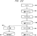
図22は、本発明の好ましい実施例に対応する動作テストベンチ・コンパイラ(behavioral testbench compiler)により作成されたソフトウェア−ハードウェア・モデルの編集に必要なステップの順序を示すフロー図である。
図22aは、本発明の好ましい実施例のLCMメモリ・ジェネレータ(memory generator)によって生成され得るメモリ回路の例を示すブロック図である。
図23は、本発明の好ましい実施例に対応するマイクロプロセッサのイベント同期バス(microprocessor event synchronaization)の共同シミュレーション・ロジック(co-simulation logic)の特別な接続を表現するために作成されたネットリスト構造のブロック図である。
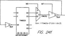
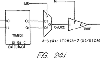
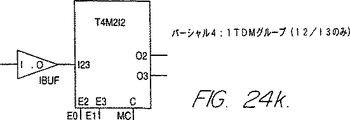
図24aは、本発明の好ましい実施例におけるロジック・チップのI/Oピンの種別に応じて挿入される時分割多重セル(time-division-multiplexing cell)の概略図である。
図24bは、本発明の好ましい実施例におけるロジック・チップのI/Oピンの種別に応じて挿入される時分割多重セルの概略図である。
図24cは、本発明の好ましい実施例におけるロジック・チップのI/Oピンの種別に応じて挿入される時分割多重セルの概略図である。
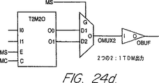
図24dは、本発明の好ましい実施例におけるロジック・チップのI/Oピンの種別に応じて挿入される時分割多重セルの概略図である。
図24eは、本発明の好ましい実施例におけるロジック・チップのI/Oピンの種別に応じて挿入される時分割多重セルの概略図である。
図24fは、本発明の好ましい実施例におけるロジック・チップのI/Oピンの種別に応じて挿入される時分割多重セルの概略図である。
図24gは、本発明の好ましい実施例におけるロジック・チップのI/Oピンの種別に応じて挿入される時分割多重セルの概略図である。
図24hは、本発明の好ましい実施例におけるロジック・チップのI/Oピンの種別に応じて挿入される時分割多重セルの概略図である。
図24iは、本発明の好ましい実施例におけるロジック・チップのI/Oピンの種別に応じて挿入される時分割多重セルの概略図である。
図24jは、本発明の好ましい実施例におけるロジック・チップのI/Oピンの種別に応じて挿入される時分割多重セルの概略図である。
図24kは、本発明の好ましい実施例におけるロジック・チップのI/Oピンの種別に応じて挿入される時分割多重セルの概略図である。
図25は、本発明の好ましい実施例のイベント検出セル(event detection cell)のブロック図である。
図26は、本発明の一実施例に対応する特別なイベント多重セル(special event-multiplexing cell)を用いて1組ごとに時間多重化されるANDツリーの出力状態を示す概略図である。
図27は、本発明の好ましい実施例のイベント検出ダウンロード回路(event detector download)のブロック図である。
図面の詳細な説明
以下に、図面を参照しながら、現時点において好ましい本発明の装置及び方法を説明する。
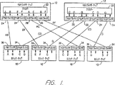
図1は、本発明のハードウェア・エミュレーション・システムの好ましい実施例のパーシャル・クロスバー・インターコネクション(partial crossbar interconnect)の一部を示したものである。パーシャル・クロスバー・インターコネクションのアーキテクチャの実施例は、本発明の譲受人と同一の譲受人に譲渡されたButts等による米国特許No.5,036,473号、5,448,496号、5,452,231号に開示されている。米国特許No.5,036,473号、5,448,496号、5,452,231号の開示内容を完全な形での参照により組み込む。パーシャル・クロスバー・インターコネクションでは、各ロジック・チップの入力/出力ピンは、各ロジック・チップで同一の分割手法を用いて適当なサブセットに分割される。各マルチプレクサ・チップ(Mux chip)(クロスバー・チップとも呼ばれる)は、各ロジック・チップの同一のサブセットに接続される。このためクロスバー・チップ‘n’は、各ロジック・チップのピンのサブセット‘n’に接続される。サブセットと同じ数のクロスバー・チップが用いられ、各クロスバー・チップは、サブセットのピンの数にロジック・チップの数を乗算した数のピンを有する。各ロジック・チップ/クロスバー・チップの組は、各サブセットのピンと同じ数の、経路と呼ばれるワイヤによって相互接続される。
図1のパーシャル・クロスバー・インターコネクションは、多くの再プログラム可能な相互接続ブロック12、好ましい実施例ではマルチプレクサ・チップ(Mux chip)により構成される。図1のパーシャル・クロスバー・インターコネクションは、さらに、複数の再プログラム可能な構成ロジック・チップ(reprogrammable configurable chip)10、現時点での好ましい実施例ではフィールド・プログラマブル(field-programmable)・ゲート・アレイ(FPGA)により構成される。各マルチプレクサ・チップ12は、各ロジック・チップ10に対して1つ又は複数の接続を有する。Buttsが開示している好ましい実施例では、ロジック・チップからマルチプレクサ・チップに向かう各設計信号は、1つの物理的相互接続を必要とする。換言すれば、ロジック・チップ10の1つのピン上の1つの信号は、マルチプレクサ・チップ12の1つのピンに相互接続される。本発明の実施例では、パーシャル・クロスバー・アーキテクチャにおける各物理的相互接続は、1つ又は複数の設計信号を表わす。
各マルチプレクサ・チップ12は、クロスバー22、複数の入力デマルチプレクサ24及び複数の出力マルチプレクサ26を有する。入力デマルチプレクサ24は、時間多重入力信号を1つ又は複数のコンポーネント信号に分割する。コンポーネント信号は、クロスバー22を介して分離して伝送される。これらの信号は、出力マルチプレクサ回路26によって、同一又は異なる組み合わせにおいて再び多重化される。好ましい実施例では、時間多重信号は、マルチプレクサ・チップ・クロスバー22を経由して伝送されない。時間多重信号をマルチプレクサ・チップ、クロスバー22を経由して伝送しないことによって、マルチプレクサ・チップに対する入力信号及び出力信号が異なる組み合わせで組み合わされるため、パーシャル・クロスバー・ネットワークをルーティング(routing)する柔軟性が向上する。これは、時間多重周波数がコンポーネント信号の平均スイッチング比よりも格段に高いため、マルチプレクサ・チップの消費電力を削減する。
ロジック・チップ10は、また、複数の入力デマルチプレクサ34及び出力マルチプレクサ36を有する。出力マルチプレクサ36は、1つ又は複数のロジック・チップ10の信号を1つの物理的相互接続に組み合わせる。入力デマルチプレクサ34は、時間多重信号を1つ又は複数の内部ロジック・チップ10の信号に分割する。現時点で好ましい実施例では、これらのマルチプレクサ36及びデマルチプレクサ34は、商業的に入手可能な既製のFPGAの内部的に構成可能なロジック・ブロックを使用して構成される。しかしながら、これらは、エミュレーションのために注文設計された再プログラム可能なロジック・チップの入力/出力ブロックを用いて構成することもできる。
図1は、専ら説明のためのものであるが、それぞれ4つのピンを有する2つのマルチプレクサ・チップ12及びそれぞれ2つのピンを有する4つのロジック・チップ10を示している。好ましいハードウェア・エミュレーション・システムの現実的な実施例では、より多くの種類のチップを有し、各チップはより多くのピンを有するであろう。マルチプレクサ・チップ12、ロジック・チップ10の実際の数及び各チップのピンの数は、純粋に設計上の選択の問題であり、達成すべき望ましいゲート容量に依存する。現時点における好ましい実施例では、各プリント回路基板は、54個のマルチプレクサ・チップ及び37個のロジック・チップ10を含む。現時点において好ましいロジック・チップ10は、4036XL FPGA(“ロジック・セル・アレイ”とも呼ばれる)であり、Xilinx Corporationによって製造されたものである。しかしながら、Altera Corporation、Lucent Technologies、Actel Corporation等によって提供される他の再プログラム可能なロジック・チップも使用可能であることに注意すべきである。現時点における好ましい実施例では、36個のロジック・チップ10が54個のマルチプレクサ・チップ12の各々に5つの接続を持っている。これは、これらの36個のロジック・チップ10の各々の5つのピンが54個のマルチプレクサ・チップ12の各々の5つのピンに対する物理的、電気的な接続を有している。37番目のロジック・チップ10は、54個のマルチプレクサ・チップのそれぞれに対して3つの接続を持っている。これは、37番目のロジック・チップ10の3つのピンが、54個のマルチプレクサ・チップ12の各々の3個のピンに物理的、電気的に接続されていることを意味する。
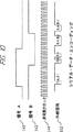
図2は、2対1の時間多重エミュレーション・システムのタイミング図であり、内部ロジック・チップ信号A40及び内部ロジック・チップ信号B42が単一の出力信号46に多重化される。多重クロック信号44は、分周クロック信号50を生成するために2分周される。同期信号48は、多重クロック分周器68(図3参照)を同期させる。すなわち、同期信号48がローレベルの時、多重クロック44の立下りエッジによって分周クロック信号50をゼロに設定する。分周クロック50は、各立ち上がりエッジで内部信号A40をサンプリングする。このサンプルは、フリップ・フロップ又はラッチ(図3参照)のような格納エレメントに格納される。同じ分周クロック信号50は、各立ち下りエッジで内部信号B42をサンプリングするために使用される。このサンプルは、他のフリップ・フロップ又はラッチ(図3参照)に格納される。好ましい実施例では、多重クロック信号44は、信号A40及び信号B42に対して非同期であってもよい。分周クロック信号50の値がハイレベルの時には、先にサンプリングされた信号A40は出力信号46に転送される。分周クロック信号50がローレベルの時には、先にサンプリングされた信号B42は出力信号46に転送される。
図3を参照すると、現時点で好ましい実施例のFPGA10内に設けられ、図2に示す信号のタイミングを作成するロジックの詳細が示されている。2対1のクロック分周器68は、多重クロック信号44を分周して分周クロック信号50を生成する。クロック分周器68は、フリップ・フロップ68a、ANDゲート68bとインバータ68cを有する。分周クロック信号50は、出力マルチプレクサ66(図1のマルチプレクサ36参照)及び入力デマルチプレクサ64(図1のデマルチプレクサ34参照)に入力される。クロック分周器68は、システム内のすべてのクロック分周器が同期化されるのを補償するために、同期信号48によって周期的にリセットされる。入力デマルチプレクサ64は、2つのフリップ・フロップ65a及び65bを有する。フリップ・フロップ65a及び65bは、多重クロック44が供給される。1つのフリップ・フロップ(例えば65b)は、分周クロック信号50がハイレベルの時にイネーブルされ、他のフリップ・フロップ(例えば65a)は、分周クロック信号50がローレベルの時にイネーブルされる。分周クロック信号50は、FPGA10の低スキュー・ライン(low-skew line)を維持するために、入力デマルチプレクサ64及び出力マルチプレクサ66のフリップ・フロップ65a、65bに対するクロックとしては直接に使用されない。フリップ・フロップ65a又は65bのいずれかの出力は、静的にデマルチプレクスされた設計信号をFPGA10のコア62(FPGA10のコア62は、ユーザー設計のロジック機能を実現するために使用される構成可能なエレメントを有する。)に供給する。出力マルチプレクサ66は、多重クロック44が供給される2つのフリップ・フロップ67a、67bを有する。出力マルチプレクサ66は、2対1のマルチプレクサ67cも有する。一方のフリップ・フロップ(例えば、フリップ・フロップ67b)は、分周クロック信号50がハイレベルの時にイネーブルされ、他のフリップ・フロップ(例えば、フリップ・フロップ67a)は、分周クロック信号50がローレベルの時にイネーブルされる。2対1のマルチプレクサ67cは、フリップ・フロップ67a又はフリップ・フロップ67bのいずれかの出力Qを選択し、出力ピンに出力する。
マルチプレクサ・チップ12に対応する回路を図4に示す。ロジック・チップ10の回路とは異なり、マルチプレクサ・チップ12の出力マルチプレクサ76(図1のマルチプレクサ26参照)は、フリップ・フロップを備えてなく、そのため、2対1のマルチプレクサ76aを有している。これは、好ましい実施例では、マルチプレクサ・チップ12を介した遅延が小さいので実現可能である。付加的なロジックを省略するために、入力デマルチプレクサ74(図1のデマルチプレクサ24参照)のフリップ・フロップ74a、74bは、イネーブル入力を持たない。その代わり、分周クロック信号50がフリップ・フロップ74a、74bに直接に供給される。クロック分周器78は、好ましくは、フリップ・フロップ78a、ANDゲート78b及びインバータ78cを有する。クロック分周器78、入力デマルチプレクサ74、出力マルチプレクサ76は、図3の対応するエレメントと同様に動作する。
マルチプレクス・チップ12の入力/出力(“I/O”)ピンが与えられた設計に対して入力又は出力となるかは前もって分からないため、マルチプレクサ・チップ12の全てのI/Oピンは、入力デマルチプレクサ74及び出力マルチプレクサの両方を含んでいる。
本発明の概念を利用することにより、ピンが、ある時点では入力となり、ある時点では出力となる、4対1の時間多重を行うことが可能である。図5は、4対1の時間多重のタイミング図を示すものである。2対1の時間多重の場合と同様に、多重クロック信号44及び同期信号48が存在する。多重クロック信号44は、分周クロック信号50を生成するために2分周される。分周器は、同期信号がローレベルで、多重クロック信号44が立ち下がった時にリセットされる。これらに加えて、分周クロック信号50をさらに2分周した追加の方向信号80が存在する。方向信号80は、各時点においてピンが入力であるか出力であるかを制御する。4つのイネーブル信号E0−90、E1−92、E2−94及びE3−96は、後述するように、ロジック・チップ10の各フリップ・フロップをイネーブルするために使用される。これらの4つの信号は、分周クロック信号50及び方向信号80から形成される。
分周クロック信号50は、外部信号98をサンプリングし、方向信号80がローレベルの時に、内部入力信号E−86及びF−88を生成する。方向信号80がローレベルの時には、ピンが入力方向で動作していることを示す。内部入力信号E−86は、分周クロック信号50の立ち上がりエッジでサンプリングによって生成される。内部入力信号F−88は、分周クロック信号50の立ち下りエッジでサンプリングによって生成される。方向信号80がハイレベルの時には、これを受信したピンは出力として動作する。内部出力信号C−82は、分周クロック信号がローレベルの時に外部信号98に出力され、分内部出力信号D(84)は、分周クロック信号50がハイレベルの時に出力される。
図6を参照すると、図5のタイミング信号を生成するためにロジック・チップ10に設けられたロジックの詳細が示されている。クロック分周器104は、多重クロック信号44を分周し、分周クロック信号50及び方向信号80を生成する。クロック分周器104は、フリップ・フロップ104a、104b、ANDゲート104c、104d、インバータ104e、イクスクルーシブORゲート(exclusive-or gate)104f、ANDゲート104g〜104jを有する。クロック・分周器104は、システム内の全てのクロック分周器104が同期されるのを補償するために、同期信号48によって周期的にリセットされる。これらに加えて、クロック分周回路104は、また、イネーブル信号E0−90、E1−92、E2−94及びE3−96を生成する。これらの信号は、入力/出力マルチプレクサ回路100及び102においてイネーブルとして使用される。
入力/出力マルチプレクサ回路100は、図5に対応するタイミングを有している。外部信号98は、方向信号80がローレベルの時に入力となる。信号E−86及び信号F−88は、イネーブル信号E0−90及びイネーブル信号E1−92がアクティブである時に外部信号98からサンプリングされ、それぞれフリップ・フロップ100a及び100bに置かれる。信号D−84及びC−82は、イネーブル信号E2−94及びE1−92がアクティブである時に、フリップ・フロップ100c及び100dにセーブされる。好ましい入力/出力マルチプレクサ回路100は、また、マルチプレクサ100e及びバッファ100fを有する。これらの構成により、フリップ・フロップ100c及び100dに予めセーブされた信号D−84及びC−82は、方向信号80がハイレベルの時に外部信号98に連続して出力される。
入力/出力のマルチプレクサ回路102は、方向信号80がローレベルの時に信号106が出力となるようにタイミングが変更されている点を除いて、同様の構成である。入力/出力マルチプレクサ102は、好ましくは、フリップ・フロップ102a〜102d、マルチプレクサ102e、バッファ102fを有する。ここで、入力/出力マルチプレクサ100を“インアウト”マルチプレクサ(inout multiplexer)と呼び、マルチプレクサ102を“アウトイン”マルチプレクサ(outin multiplexer)と呼ぶものとする。ピンがシステム内で互いに接続されている時、一方のピンがドライブ(drive)し、他方のピンが読み取る(即ち、信号の受信準備ができている又は信号を受信中)ことができるように、インアウト・ピンは常にアウトイン・ピンに接続されている必要がある。
対応する4線(4-way)の時間多重回路を、図7にマルチプレクサ・チップ12として示す。クロック分周器132は、分周クロック信号50及び方向信号80を生成する。クロック分周器132は、フリップ・フロップ132a、132b、ANDゲート132c、132d、インバータ132e及びイクスクルーシブORゲート132fを有する。ロジック・チップ10と同様に、インアウト・マルチプレクサ120及びアウトイン・マルチプレクサ122が存在する。インアウト・マルチプレクサ120は、好ましくは、フリップ・フロップ120a、120b、2対1マルチプレクサ120c及びバッファ120dを有する。インアウト・マルチプレクサ120は、図5に示すタイミングを有する。外部信号98は、方向信号80がローレベルの時に入力となり、方向信号80がハイレベルの時に出力となる。内部信号124及び126は、方向信号80がローレベルの時に外部信号98からサンプリングされる。内部信号128及び130は、方向信号80がハイレベルの時に外部信号98に出力される。
アウトイン・マルチプレクサ回路122は、信号134が、方向信号80がハイレベルの時に入力となり、方向信号80がローレベルの時に出力となるようにタイミングが変更されている点を除いて、同様の構成である。アウトイン・マルチプレクサ122は、好ましくは、フリップ・フロップ122a、122b、2対1のマルチプレクサ122c及びバッファ122dを有する。マルチプレクサ・チップ12のアウトイン・ピンは、他のマルチプレクサ・チップ12又はロジック・チップ10のインアウト・ピンに接続する必要がある。付加的な構成ビット(configuration bit)(図7に図示していない)により、マルチプレクス・チップ12の任意のピンを、多重化(non-multiplexed)されていない入力又は出力、2対1に多重化された入力又は出力としても、4対1に多重化されたインアウト・ピン又はアウトイン・ピンとしてもプログラム可能に構成することができる。これは、選択的に、方向信号80を常にローレベル(2対1入力に対応)、常にハイレベル(2対1出力に対応)、非反転状態(120のようなアウトイン・4対1ピンに対応)とし、又は反転状態(122のようなアウトイン・4対1ピンに対応)とすることによって実現される。これらに加えて、外部信号98は、非多重化入力に対応して、コア信号124に直接に接続することができる。コア出力128及び130は、非多重化入力に対応して、バッファ120dの入力及びイネーブル・ピンに直接に接続することができる。
好ましい実施例では2対1及び4対1の時間多重を採用しているが、ここに開示された技術は、設計者によって選択されるあらゆる他の要因による多重化についても拡張して適用することができる。一般的には、高度に多重化を行うと、エミュレーション速度は低下するが、物理的なワイヤ及びピンをより多くのロジック設計信号間で共有することができるため、ハードウェアを簡略化することができ、低コストとなる。
さらに、エミュレーション・システムに使用可能な、情報の複数のビットを1つの物理的ワイヤに多重化する多くの他の方法が存在する。これらの技術の例としては、パルス幅変調、位相変調及びシリアル・データ・エンコーディング等がある。特定の実施例どの方法を選択するかは、設計者の選択の問題であり、動作速度、コスト、消費電力及び必要とされるロジックの複雑さの間での相対関係に依存する。
ハードウェア・エミュレーション・システムにおいて重要となるこれらのさらに複雑なエンコーディング手法の一側面は、消費電力を低減することができることである。ハードウェア・エミュレーション・システムは、通常、数千の相互接続経路を有している。システムを通じた遅延を最小化するために、これらの相互接続経路を異なるロジック設計信号の間でできるだけ速く切り替えることが望ましい。しかしながら、システムの消費電力は、相互接続経路が切り替えられる速度に大きく依存している。大規模なシステムでは、電力の生成及び分配とこれに伴う発熱の除去のために、システムの複雑さとコストが大きく増大する。このため、高速で動作するが、大きな電力を必要としない多重方式を採用することが望ましい。消費電力を最小化する方法の1つとして、設計信号を連続して転送するのではなく、設計データが変更された時にのみ設計信号情報を転送するものがある。この方法は、現時点での好ましい実施例で採用されている。
エンコーディング方法を選択する時に考慮すべき他の重要な観点は、相互に非同期で又はマスタ・多重クロック(master multiplexing clock)に非同期で動作する相互接続を有することができることである。前記した、現時点での好ましい実施例に対応する時間多重の簡単な形式では、マスタ・多重クロックを、低スキュー(low skew)でシステム内の全てのロジック・チップ10及びマルチプレクス・チップ12に分配する必要がある。これに加えて、マスタ・多重クロックは、システム内の最も長い相互接続上を信号が通過可能であるように十分に低い速度とする必要がある。同時に、システム内の最も短い相互接続においてホールドタイム違反(hold-time violation)が発生してはならない。ホールドタイム違反は、受信装置がデータ信号をフリップ・フロップ又はラッチに適切にセーブする前に、送信装置がデータ信号を除去することによって生じ得る。低スキューの、マスタ・クロックに対する要求によって、エミュレーション・システムの複雑さとコストは大幅に増大する。これに加えて、想定可能な最短データ経路上でのホールドタイム違反を防止するとともに、想定可能な最長データ経路上を信号が通過するのに十分な時間を確保することは、多重クロックが比較的低速で動作しなければならないことを意味する。すでに説明したとおり、これは、エミュレーション・システムの実効的な動作速度を限定するため、好ましくない。
前記した、時間多重の最も簡単な形式に関する発明の概念は、より複雑なエンコーディング方法にも同様に適用可能である。以下に、それを説明する。パルス幅変調、位相シフト変調及びシリアル・エンコーディングを用いたエンコーディング方法は、消費電力を低減し、最も簡単な形式の時間多重に本質的な問題である比較的低い動作速度を増加させることができる。これらのすべての手法の欠点(簡単な時間多重に関して)は、これらが格段に多くのエンコーディング・ロジック及びデコーディング・ロジックを必要とすることである。このため、現時点での好ましい実施例では、簡単な時間多重が用いられていた。デジタル・ロジックのコストが物理的なピンや回路基板経路(circuit board trace)のコストに比較して減少するにつれ、将来的には、1つ又は複数のこれらのより複雑なエンコーディング手法が使用されることとなろう。
図8を参照すると、ハードウェア・エミュレーション・システムに適すると思われるパルス幅変調の1つの形式が示されている。外部信号146は、通常はローレベルである。設計信号140又は142が変化すると、パルスが外部信号146に出力される。高速の非同期クロック信号144は、システム内の全てのチップに分配される。図2を参照して述べた多重クロック44とは異なり、非同期クロック信号144は、システム内の任意の2つのチップ間、又は同じチップの2つのピンの間であっても同期化する必要がない。そのため、図2を参照して述べた同期信号48は必要ない。また、非同期クロック144は、外部信号144に生成される最小パルス幅が品質の劣化を伴わずに相互接続を介して通過することができる限り、任意の速度で動作させることができる。外部信号146に出力されるパルスは、2つの設計信号140及び142の信号変化時点における値が00、01、10又は11であるか否かに応じて、1つ、2つ、3つ又は4つのクロックの幅を有する。しかしながら、非同期クロック信号144は、情報が失われることがないように、設計信号140及び142の連続するエッジの間に常に5つのクロック・サイクルが経過するよう十分に高速でなければならない。データ信号140及び142は、外部信号146がハイレベルとなるたびに発生する非同期クロック144のサイクル数をカウントすることにより、外部信号146から再生することができる。現実の実施例では、非同期クロック144は、再生された信号が明確に判別できるように、ここに示す速度の2倍又は3倍の速度で動作することになるであろう。また、付加的な回路は、設計信号が変化しない場合でも設計を適正に初期化できるようにするために、周期的にデータを転送するための付加回路が加えられる。
設計信号140及び142は、非同期クロック144と平均的に比較して比較的頻繁には変化しないため、消費電力は、前記した連続的な時間多重に比べて低くなる。それに加えて、このエンコーディング手法は、送信回路及び受信回路の間の遅延量の変化の影響を受けない。
このパルス幅エンコーディング手法を実現するために必要なロジック回路は、回路設計の分野における当業者によって設計が可能である。ここでは、これ以上論じない。しかしながら、当業者は、同じ機能を実現する、多くの異なった種類のロジック回路を設計することができることに注意すべきである。例えば、2つではなく、3つの設計信号を1つの外部信号146にエンコードすることができる。また、設計信号140及び142の異なるエンコード手法を用いることができ、又は外部信号146のデフォルト値を0ではなく1とすることもできる。
図8に示したパルス幅変調エンコーディング手法は、以下の制約がある。パルス幅変調エンコード手法では、パルス幅は、外部信号146の立ち上がりエッジから外部信号146の立ち下りエッジの間で測定される。しかしながら、信号がルーティング・チップ(routing chips)の多くのレベルを通過する時、立ち上がりエッジは、しばしば、立ち下りエッジとは異なる遅延が発生する。このため、信号多重の速度は、ルーティング・チップの多くのレベルを通過した後でも信号の値を判別することができるように、低速化する必要がある。また、図8の変調手法は、避けることのできない一時的な信号の変化又は外部信号146のグリッチに敏感である。このため、誤った信号の値が送信される可能性がある。
図9を参照すると、ハードウェア・エミュレーション・システムに適していると思われる位相変調の一方式を示す。内部の位相ロックループ(“PLL”)回路は、入力として非同期クロック144を用い、連続的に0から3までカウントする(図9のPLLカウント150参照)。このPLL回路は、一般的にデジタル位相ロックループ(“DPLL”)と呼ばれるもので、相補型の金属酸化半導体(“CMOS”)集積回路技術を用いて比較的簡単に構成することができる。設計信号の140又は142に変化が生じると、外部信号152は、設計信号140及び142の値に依存した時間に変化する。例えば、信号A−140の最初の変化の後では、信号A−140及び信号B−142の両方がハイレベルとなる。そのため、外部信号152は、PLLがカウント3の状態(A、B=11)の時に変化する。その後、信号B−142の変化の後で、信号A140がハイレベルとなり、信号B−142がローレベルとなる。このため、外部信号152は、PLLがカウント2の状態(A、B=10)の時に変化する。
受信回路は、転送すべきデータがない時に定期的に送信される同期パルスによって送信PLLとの同期状態を保持される、マッチングPLLを有する。同期パルスは、送信PLLの時間0及び時間2において発生する2つの変化により構成される。1つのPLLサイクル内で外部信号152に2つの変化が生ずるのは同期パルスが送信される時のみであるため、同期パルスは、受信PLLによって認識することができる。同期パルスによって受信PLLのカウントが除々に調整され、いくつかの同期パルスが発生した後に受信PLLは送信PLLと同期状態となる。同期パルスは、信号A−140及び信号B−142の変化に比べて比較的少ない頻度で発生させれば充分であるため、消費電力は大きくは増加しない。現実の実施例では、非同期クロック144は、外部信号152の異なるエッジ変化時間の間を明確に区別するのに十分な分解能を持たせるために、図9に示す速度の2倍又は3倍の相対速度で動作させることになるであろう。代わりに、分解能を向上させるために、位相ロックループを非同期クロック144の周波数の数倍の速度で動作させることもできる。また、設計信号A−140及び設計信号B−142が変化していない場合でもその値を定期的に送信する回路を付加し、設計が適正に初期化されるようにすることもできる。
この位相エンコード手法で用いられる、デジタル位相ロックループを構成するために必要な回路、送信及び受信回路は、回路設計の技術分野における当業者によって設計可能であり、ここでは、これ以上論じない。
前記した位相変調エンコード手法は、これまでに論じたパルス幅変調手法(図8参照)に対していくつかの利点を有する。図8の外部信号146の場合に比べて、信号A−140及び信号B−142の値を送信するために必要な外部信号152の変化が少ない。これにより、システムによって消費される電力が低減される。また、故障(glitch)パルス又は短パルスは同期パルスとして扱われ、PLLカウント150は除々に影響を受けるのみであるため、ノイズに対する回路の感度を引き下げることができる。これに加えて、同期パルスは常に1つの立ち上がりエッジと1つの立ち下りエッジを有しているため、立ち上がりエッジと立ち下りエッジを計時するために別個のPLLカウンタを使用することができる。立ち上がりエッジと立ち下りエッジを個別に計時することにより、非同期クロック144は、非常に高い周波数で動作することができるとともに、信号A−140及び信号B−142の再生の信頼性に影響を与えることなく、外部信号152を中間のルーティング・チップを介して通過させることができる。しかしながら、位相変調の主な欠点は、比較的大量のデジタル・ロジックを組み込む必要があることである。
ここに開示した位相変調エンコード手法については、本発明の趣旨を逸脱することなく様々な変更を加えることができる。例えば、PLLは、4つ以外の8又は16の変化時点を認識することができる。また、設計信号に変化が発生する毎に外部信号152に複数のエッジを作成することによって、付加的な設計信号を送信することができる。例えば、設計信号A及びBは、外部信号152の最初のエッジで送信することができ、設計信号C及びDは、外部信号152の2番目のエッジで送信することができる。これにより、外部信号152でより多くのデータを送信できるという効果を生じるが、速度は低くなる。
図10を参照すると、ハードウェア・エミュレーション・システムに使用可能と思われる、変調の他の形式が示されている。この技術は、シリアル・データ・エンコーディングと呼ばれている。RS232C等の多くの一般的なプロトコルでは、シリアル・データ・エンコーディングの変形を使用している。設計信号A−140又は設計信号B−142が変化すると、データのシリアル・ストリング(serial string)が外部信号162に送信される。常に0であるスタート・ビットは、送信が開始されることを示す。次に、信号A−140及び信号B−142の値が連続して送信される。最後に、常に1であるストップ・ビットが送信される。受信回路は、信号A−140を再生するために外部信号162をサンプリングする前に、非同期クロック信号144を使ってスタート・ビットの立ち下りエッジから1及び1.5クロックだけ遅延させる。そして、信号B−142を再生するために外部信号162をサンプリングする前に、さらに1クロック遅延させる。現実の実施例では、信号A−140及び信号B−142が送信されている時、外部信号162をその中央点で正確にサンプリングするために、非同期クロック144は、図10に示す周波数より数倍高い周波数で動作することになろう。
シリアル・データ・エンコード手法を構成するために必要な回路は、回路設計の技術分野における当業者によって設計可能であり、ここでは、これ以上論じない。
シリアル・データ・エンコーディングは、比較的簡単なデジタル・ロジックを使用できるという利点がある。しかしながら、設計信号A−140及び設計信号B−142に対する変化を送信する毎に外部信号162に複数のエッジが必要であるという欠点がある。これは、データ・レートが比較的低く、他の技術に比較して消費電力が比較的に高いことを意味する。
ここで開示したシリアル・データ・エンコード手法については、本発明の趣旨を逸脱することなく様々な変更を加えることができる。例えば、設計信号が変化した時毎に、2つ以上の設計信号の値を送信することもできる。
図8〜10に示す各エンコード手法は、いくるかの形式のエラー・チェック技術を追加することによってさらに改良することができる。設計データは設計信号が変化したときにのみ送信されるため、送信エラーが発生すると、受信回路によって誤ったデータ値がラッチされることになり、またエミュレーションが誤動作する可能性がある。パリティ・チェックや巡回型冗長性チェック(CRC)等の一般的なエラー検出を用いることができる。
好ましい実施例のシステム面をさらに詳細に開示する。図11を参照すると、ロジック・チップ(現時点での好ましい実施例ではFPGA)及びマルチプレクサ・チップ12を組み込んだ、好ましい実施例のロジック・ボード200のブロック図が示されている。ロジック・ボード200は、Buttsらによって開示されたものに類似するパーシャル・クロスバー・インターコネクションを有している。主な相違点は、本発明の現時点での好ましい実施例のパーシャル・クロスバーは、後述するロジック・チップ204に接続されているマルチプレクサの数が他のロジック・チップより少ないため、完全に同型(uniform)になっていないことである。現時点での好ましい実施例では、それぞれが260個のI/Oピンを有する54個のマルチプレクサ・チップ12及びそれぞれが270個のI/Oピンを有する36個のロジック・チップ(FPGA)がある。現時点での好ましい実施例では、Xilinx Corporation,San Jose,California,U.S.A.により製造された部品番号XC4036XLのFPGAをロジック・チップ10として使用する。36個のロジック・チップ10の各々は、54個のマルチプレクス・チップ12の各々との間に5つの接続を有している。37番目のロジック・チップ204は、ここでは共同シミュレーション(co-simulation)(CoSim)として知られているが、54個のマルチプレクサ・チップの各々との間に3つの接続を有している。現時点での好ましい実施例では、37番目のロジック・チップ204も、Xilinxによって製造された部品番号4036XLのFPGAである。マルチプレクサ・チップ12及びロジック・チップ10、204の追加のピン(図示していない)は、ダウンロード、クロック分配及び他のシステム機能のために確保されている。以下に、CoSimロジック・チップの目的を説明する。任意のマルチプレクサ・チップ12からロジック・チップ10への接続は、マルチプレクサ・チップ12及びロジック・チップ10を適当にプログラムすることにより、非多重、2対1の多重、4対1の多重とすることができる。
前記した相互接続に加え、CoSimロジック・チップ204も、プロセッサ206と電気的に通信を行う。現時点での好ましい実施例では、プロセッサ206は、IBM Corporationから入手可能なPowerPC 403GCチップである。プロセッサ206は、共同シミュレーションのために使用される。これは、Sampleらによる「Method And Apparatus For Design Verification using Emulation And Simulation」という名称の米国特許第5,841,967号に開示されている。参考のため、米国特許第5,841,967号の開示内容をここに組み入れる。プロセッサ206は、診断機能や、マルチプレクサ・チップ12、ロジック・チップ10、204、RAM208(以下に説明する)及びSGRAM210(以下に説明する)への情報のダウンロードに使用される。プロセッサ206は、VMEインターフェース(図示していない)を介してバックプレーン・コネクタ(backplane connector)220に接続される。また、12個のロジック・チップ10は、32個の静的・ランダム・アクセス・メモリ(static randomacess memory)(RAM)・チップ208によって32Kに接続される。このRAMチップ208は、エミュレートされる回路の一部となり得る大きなメモリを構成するために使用される。また、RAM208は、ロジック・チップ10をマルチプレクサ・チップ12に接続している線の一部に取り付けられる。このようにして、RAMが使用されていない場合には、ロジック・チップ10からマルチプレクサ・チップ12への接続は、通常の相互接続機能として使用することが可能であり、これらが失われることはない。RAM208が特定のネットリストの一部のメモリを構成するために必要とされる場合には、それと通信するロジック・チップ10にはRAMコントローラ機能がプログラムされる。
マルチプレクサ・チップ12は、バック・プレーン・コネクタ220及びターボ・コネクタ(turbo connector)202との間にも接続を有している。バック・プレーン及びターボとの接続は、非多重、2対1の多重あるいは4対1の多重のいずれでもよい。ターボ・コネクタ202は、2つのロジック・ボード200をサンドウィッチの形で電気的に接続するために使用される。2つのロジック・ボードを1組として直接に接続することにより、特定の設計について必要とされるバックプレーン接続が軽減される。バックプレーン・コネクタは、ロジック・ボードの一辺に沿って適合するものでなければならず、可能なバックプレーン接続の数は利用可能なコネクタの種類によって限定される。不十分なバックプレーン接続が存在する場合には、パーティショニング・ソフトウェア(partitioning software)は、効率的に動作することができず、ボードのロジック容量は低下する。サンドウィッチ状に接続された2つのエミュレーション・ボードを図13に示す。2つより少ないエミュレーション・ボードから成る小規模なエミュレーション・システムが要求される場合には、ロジック回路が配設されていない特別のターボ・ループバック・ボード(turbo loopback board)が使用される。このようなシステムでは、この特別なターボ・ループバック・ボードは、ターボ・コネクタ202からバック・プレーン・コネクタ220に信号をルーティング(route)する。ターボ・ループバック・ボードを使用した構成の例を図15に示す。
これに加えて、マルチプレクス・チップ12は、1組の同期グラフィックRAM(SGRAM)210に対する8つの接続を有する。これらのSGRAM210は、分配されたロジック・アナライザのデータ経路を形成するために使用される。設計信号は、ロジック・チップ10及びCoSimロジック・チップ204でサンプリングされ、マルチプレクサ・チップ12を介してルーティングされ、そしてユーザによる将来的な解析のためにSGRAM210にセーブされる。ロジック・アナライザについて、以下で説明する。
ロジック・チップ10及びCoSimロジック・チップ204は、また、イベント・バス212及びクロック入力・バス214が設けられている。イベント・バスは、イベント信号をロジック・チップ10及びCoSimロジック・チップ204内からロジック・アナライザ制御回路(以下に説明する図20a参照)にルーティングする。イベント・バスは、4つの信号により構成され、8つの信号を供給するために2対1に時間多重化される。イベント・バス212の信号は、バッファに格納され、そしてバックプレーン・コネクタ220上の付加ピン(図示していない)にルーティングされる。
バス214のクロックは、すべてのロジック・チップ10及びCoSimロジック・チップ204(以下に説明する)にルーティングされる8つの低スキューの特別目的のクロック・ネット(clock net)により構成される。バス214のクロックは、米国特許No.5,475,830号に説明されているように、クロック信号を分配するために使用される。バス214のクロックからのクロックは、バック・プレーン・コネクタ220上の付加ピン(図示していない)に接続される信号218からバッファ216を介して直接的に送られ、又は主クロック信号をCoSimロジック・チップ204内のロジックと組み合わせることによって作成される。CoSimロジック・チップ204がクロック・ロジックを供給するために使用されている場合には、米国特許No.5,475,830号説明されているように、“クロック生成FPGA”として動作する。
図12参照すると、ボード間の相互接続が示されている。ロジック・ボードは、ターボ・コネクタ202を介して接続される一対として組み立てられる。ロジック・ボードは、また、バックプレーン・コネクタ220(図11参照)介してスイッチング・バックプレーン420に接続される。スイッチング・バックプレーン420は、ロジック・ボードに直角に配設されたマルチプレクサ・ボード400により構成される。ロジック・ボード及びスイッチング・ボードの配置は、本発明の譲受人と同一の譲受人であるSampleらに譲渡された米国特許No.5,352,123号に開示されている。米国特許No.5,352,123号は、参考のために、ここに完全な形で組み込まれる。スイッチング・バックプレーン420は、また、I/Oボード300に接続されている(図12では、1つのI/Oボードのみが示されている。しかしながら、複数のI/Oボード300を使用することも、本発明の一部であると考えられる。)。I/Oボード300は、コア・ボード500又は外部システム540に含まれる外部装置からの信号をルーティングするとともにバッファする機能を提供する。また、これらは、すべての外部ピンに対して刺激信号(stimulus signal)を提供する能力を有している。それによって、エミュレートされる設計は、外部装置又は外部システムが無い場合でも動作可能である。
I/Oボード300は、コア・ボード500及びリピータ・ポッド520を介して外部システム540に接続される。簡略化のため、図12では、現実のボード及び接続の数より低減されている。現時点における好ましい実施例では、22個のマルチプレクサ・ボード400、1から10対のロジック・ボード200及び最大8個のI/Oボード300が存在する。現時点における好ましい実施例では、2以上のI/Oボードが使用されると、一対のロジック・ボード200は、追加のI/Oボード300の対の各々について失われる。現時点における好ましい実施例では、各I/Oボード300は、ケーブルに取り付けられる、最大7つのリピータ・ポッド520を有するコア・ボード500を1つ有している。現時点における好ましい実施例における各リピータ・ポッドは、88の双方向信号をバッファする。
図13は、好ましい実施例のシステムの物理的な構成を示したものである。マルチプレクサ・ボード400は、ロジック・ボード200及びI/Oボード300に対して直角に設けられている。バックプレーン800は、一方側にマルチプレクサ・ボード400に対するコネクタを有し、他方側にロジック・ボード200又はI/Oボード300に対するコネクタを有する。図面の簡略化のため、1つのマルチプレクサ400及び3対のロジック・ボード200のみを示している。しかしながら、現時点における好ましい実施例では、現実には、22個のマルチプレクサ・ボード400及び最大7対までのロジック・ボード200又はI/Oボード300が存在する。I/Oボード300は、コネクタ330を介してコア・ボード500に取り付けられている。コア・ボード500は、外部コネクタ510を有している。外部コネクタ510は、ケーブルを介してリピータ・ポッド520及び外部システム540(図13に示していない)に装着される。電源ボード240は、48VのDC主電源を、ロジック・ボードの電源供給のために必要な3.3Vに変換する。この種の分配電源変換は、時間多重回路の電源に対する高い要求によって必要となる。これに加えて、システムは、コントロール・ボード600及びCPUボード700(図20参照)を含む。現時点での好ましい実施例では、CPUボード700は、Themis Computerやその他から入手可能な、VMEバス対応のPower-PCプロセッサ・ボードである。他の同様なプロセッサボードを利用することも可能である。使用する特定のプロセッサボードの選択は、コスト、速度、RAM容量及びその他の要因の間での相対関係に依存する。CPUボード700は、ネットワーク・インターフェースを提供し、エミュレーション・システムを総合的に制御する。コントロール・ボード600は、クロック分配、ダウンロード及び他のボードのテスト機能を提供するとともに、ロジック・アナライザ及びパターン・ジェネレータ(構造及び機能は以下で説明する)の集中化機能を提供する。
また、現時点において好ましいエミュレーション・システムの縮小バージョンを構成することもできる。このシステムのブロック図を図14に示す。縮小されたシステムは、スイッチング・バックプレーン420を持たない。その代わり、ロジック・ボード200は、互いに直接に接続され、またI/Oボード300に接続される。これは、システムのサイズが二対のロジック・ボード200及び一対のI/Oボード300に限定されため、可能である。バックプレーン接続は、図14の上部に示される。各バックプレーン・コネクタ220からのピン(図11に示されている)は、4つの等しいグループに分割される。各グループは、バックプレーンを介して、同一の対に含まれない2つのロジック・ボード200の1つ及び各I/Oボード300にルーティングされる。接続は、ロジック・ボード200の場合にはターボ・コネクタ202を介して提供され、I/Oボード300の場合には接続を必要としないため、同一の対に含まれる他のロジック・ボード200又はI/Oボードに対してはバックプレーンを介して接続する必要はない。図14に示す接続パターンは、ボード間の十分に余裕のあるルータビリティ(routability)を提供するが、スイッチング・バックプレーン420が高価となるのを避ける。大規模なシステムでは、I/Oボードは、コア・ボード500及びリピータ・ポッド520を通じて外部システム540に接続される。図面の簡略化のために、第2のボードに対して、コア・ボード500、リピータ・ポッド520及び外部システム540が現実には存在するが、示していない。追加のボードの組を、そうしなければ使われることのないバックプレーン及びターボ・コネクタの間を接続するために使用することにより、小規模なシステムのバージョンは、1から4個のロジック・ボード200及び1個又は2個のI/Oボード300のいずれかによって構成することができる。これらの追加ボードは、図15に示されているターボ・ループバック・ボード260及びバックプレーン・ループバック・ボード280である。これらのボードのいずれもデジタル・ロジックを有していない。これらは、コネクタ間で信号をルーティングするに過ぎない。
1つのロジック・ボード及び1つのI/Oボードを有する小規模なシステムの物理的な図を図15に示す。バックプレーン802は、これまでに図14を参照しながら説明した接続を提供する。I/Oボードは、コネクタ330を介してコア・ボード500に接続される。コア・ボード500は、ケーブルを介してリピータ・ポッド520及び外部システム540(図15には図示していない)を装着する外部コネクタ510を有する。電源ボードは240、48VのDC主電源をロジック・ボードの電源供給のために必要な3.3Vに変換する。これに加え、小規模なシステムは、これまでに図13を参照して説明した大規模システムのように、コントロール・ボード600及びCPUボード700を含む。4個以下のロジック・ボードが使用される時、ルーティング接続を確保するために、ターボ・ループバック・ボード260は、ロジック・ボード200の使用されていないターボ・コネクタ202(図11に示されている)からの信号をバック・プレーン802に接続する。ターボ・ループバック・ボード260は、システム内の1つ又は3つのロジック・ボード200が存在する場合に使用される。追加のバックプレーン・ループバック・ボード280の対は、使用されていないロジック・ボード・スロットがある時に、バックプレーンを介したルーティング接続を確保するために使用される。これは、システム内に1つ又は2つのロジック・ボードが存在する場合に発生する。バックプレーン・ループバック・ボード280は、バック・プレーン信号(図4に示されている)のグループを互いに接続して、空のバックプレーン・コネクタが存在する時に信号が失われないようにする。
図16に、I/Oボード300及びコア・ボード500のブロック図を示す。マルチプレクサ・チップ12の第1列301は、I/Oボード300のバックプレーン・コネクタ320に装着される。図の簡略化のため、3つのマルチプレクサ・チップ12のみが第1列301に示されている。しかしながら、現時点における好ましい実施例では、最初の列301には14個のマルチプレクサ・チップ12が存在する。マルチプレクサ・チップ12の第2列303は、マルチプレクサ・チップ12の第1列に接続されるとともに、電界効果型トランジスタ(FET)308及びロジック・チップ304に接続される。ここでも、図面は、簡略化されて、2つのマルチプレクサ・チップ12だけが示されている。現時点における好ましい実施例では、第2列303には12個のマルチプレクサ・チップ12が存在する。マルチプレクサ・チップ12の2つの列301、302は、ルーティングにおける十分な柔軟性を達成することが要求される。それにより、任意の外部信号を、コア・ボード500のリピータ・ケーブル・コネクタ510の任意のピンに接続することができる。ロジック・チップ304も、同期グラフィックRAM(SGRAM)302に装着される。現時点における好ましい実施例では、ロジック・チップ304は、FPGAである。1つのロジック・チップ304と1つのSGRAM302のみが示されているが、現時点における好ましい実施例では、I/Oボード300には6個のロジック・チップ304及び3個のSGRAM302が存在する。ロジック・チップ304及びSGRAM302は、刺激ベクトル(stimulus vector)を外部接続ピン上のエミュレータにドライブする能力を提供する。刺激ベクトルをドライブする時には、FET308はターンオフされる(即ち、開放される)。これにより、刺激が、リピータ・ポッド520を介してコネクタ510に装着することのできる外部システムからの信号と競合を生じないようにする。刺激ベクトルをドライブしない時には、ロジック・チップ304のピンは、トライステートされ(tristate)、FET308がターンオンされる(即ち、閉じられる)。これにより、コネクタ510の信号は、第2列のマルチプレクサ・チップ303からの信号をドライブ又は受信することができる。現時点における好ましい実施例では、ロジック・チップ304は、Xilinx Corporation,San Jose,Californiaから入手可能なXC5215であるが、他のプログラム可能なロジック・チップを使用することによっても満足すべき結果を得ることができる。図16に示す部品に加えて、I/Oボード300は、VMEインターフェースを通じてバックプレーン・コネクタ320に接続されるプロセッサ・チップ(図示していない)を含む。現時点における好ましい実施例では、このプロセッサ・チップは、IBM Corporationから入手可能なPowerPC 403GCであるが、他のマイクロプロセッサ・チップを用いることによっても満足すべき結果を得ることができる。プロセッサのチップは、プロセッサ・バス310を介してロジック・チップ304に装着される。プロセッサ・バス310は、刺激情報をSGRAM302にアップロードする働きをする。プロセッサは、診断機能のため、マルチプレクサ・チップ12、ロジック・チップ304及びSGRAM302からの情報をアップロード及びダウンロードするために使用される。
コネクタ330は、コア・ボード500をI/Oボードに装着する。FET308から送られるロジック信号に加えて、このコネクタ330は、JTAG信号を受信し、電気的にVMEバスに接続される。JTAG信号は、コネクタ510に差し込むことのできるリピーター・ポッド520をダウンロード及びテストするためのものである。現時点における好ましい実施例では、VMEバスは、コア・ボードと共に使用されていない。しかしながら、VMEバスは、コネクタ330に差し込むことができる他の種類のボードとともに使用することが考えられる。例えば、大容量のメモリ・ボードをコネクタ330に差し込んで、RAM208に収納可能なメモリよりも大きなメモリをエミュレートする能力を提供することが考えられる(図11に示されている)。
図17を参照すると、マルチプレクサ・ボードのブロック図が示されている。マルチプレクサ・チップ12は、バックプレーン・コネクタ420に対して分配される形で装着される。図17の簡略化のために、4つのマルチプレクサ・チップ12のみが示されている。しかしながら、現時点における好ましい実施例では、実際には、マルチプレクス・ボード400には7個のマルチプレクサ・チップが存在する。さらに、マルチプレクサ12への接続は、図17に示されている数よりはるかに多く存在する。これらの追加の接続は、図示されたものと同様に配置される。図17に示すマルチプレクサ・チップ12に加えて、マルチプレクサ・ボード400は、バックプレーン・コネクタ420に装着され、マルチプレクサ・チップ12にダウンロードし又はテストするJTAGインターフェース(図示していない)を含んでいる。
図17のマルチプレクサ・ボードは、拡張性のないエミュレーション・システムに適している。しかしながら、いくつかのエミュレーション・システムを互いに接続することによって、大容量のエミュレーション・システムを構成することが、しばしば要望される。この場合には、拡張性のあるマルチプレクサ・ボード400が使用される。拡張可能なマルチプレクサ・チップ・ボード402のブロック図を図18に示す。マルチプレクサ・チップ12の第1列404は、バックプレーン・コネクタ420に電気的に接続されている。図面の簡略化のため、第1列404には、4つのマルチプレクサ・チップ12のみが示されている。しかしながら、現時点における好ましい実施例では、第1列404には、10個のマルチプレクサ・チップ12が存在する。マルチプレクサ・チップ12の第1列404は、マルチプレクサ・チップ12の第2列406及びターボ・コネクタ430に電気的に接続される。マルチプレクサ・チップ12の第2列406は、また、ターボ・コネクタ430及び外部コネクタ440に電気的に接続される。図18には、第2列には、2つのマルチプレクサ・チップ12のみが示されており、そして2つの外部コネクタ440のみが示されている。しかしながら、現時点における好ましい実施例では、第2列406には、5個のマルチプレクサ・チップ12が存在する。さらに、現時点における好ましい実施例では、6個の外部コネクタ440が存在する。現時点における好ましい実施例の各外部コネクタ440は、92個のI/Oピンを有している。マルチプレクサ・ボード402は、ターボ・コネクタ430を介して互いに結合された対に組み立てられる。ターボ・コネクタ430は、マルチプレクサ・ボード402の対とロジック・ボード200の対の間の有効な交差領域(intersection area)を拡張する役割を果たす。ターボ・コネクタ430が無い場合には、交差領域が小さくなりすぎて、外部コネクタ440とロジック・ボード200の間での有効なルーティング性能(routability)を確保することができない。
図19を参照すると、エミュレーション・システム内におけるユーザ・クロックの分配方法が示されている。ユーザ・クロックの分配は、エミュレーション・システムの設計において重要である。米国特許No.5,475,830号に開示されているように、ユーザ・クロックは、ユーザー・クロック及びデータ信号が外部システム540(外部システムは、図12及び14に示されている。)内で同時に変化すると仮定すると、データ信号の前にエミュレーション・ボード200のロジック・チップ10に到達する必要がある。この要求は、データ信号を遅延させることにより満足させることができる。しかしながら、この解決方法では、エミュレーション・システムの最大動作速度が低下する。より好ましい代替案は、ユーザ・クロックの分配ネットワークをできる限り高速とし、データ信号に遅延を付加する必要があるとしても、遅延を最小限とすることである。
図19に、好ましいハードウェア・エミュレーション・システムに対するクロックの分配を示す。クロックは、コントロール・ボード600のクロック・コネクタ620を介して、コントロール・ボード600のマルチ・ボックス・クロック・コネクタ630を介して、又はコア・ボード500のコネクタ510の通常の信号としてのいずれかによってシステムに入力することができる。前述したように、コア・ボード500は、I/Oボード300に装着されている。簡略のため、図19には、1つのコネクタのみが示されている。しかしながら、現時点における好ましい実施例では、各コア・ボード500には7つのコネクタ510が存在する。また、システムは、複数のI/Oボードとコア・ボードの組み合わせを含めてもよい。これまでに図12及び14を参照して説明したように、コネクタ510は、外部システム540に接続されるリピータ・ポッド520に装着されている。クロック・コネクタがクロックを入力するために使用される場合には、コネクタ620も、ケーブルを通じて外部システム540に装着されるであろう。クロック・コネクタ620は、クロックをエミュレーション・システムに入れるための速い方法を提供し、コア・ボード500のコネクタ510は、より簡単な方法をユーザーに提供する。
コア・ボード500のコネクタ510は、これまでに図16を参照して説明したように、コネクタ330及びFET308を介してI/Oボード300上のマルチプレクサ・チップ12の第2列に接続される。マルチプレクサ・チップ12の第2列303は、これまでに説明した他の接続に加えて、バックプレーン・コネクタ320の専用クロック・ピンに接続される。現時点における好ましい実施例では、これらのピンは16本存在する。I/Oボードのバックプレーン・コネクタ320から、クロックは、バックプレーン800又は802を介してコントロール・ボード(図13参照)に接続する。コントロール・ボード600では、マルチプレクサ・チップ12は、異なる可能性を有する全てのソースの中から1つのクロックの組み合わせを選択するために用いられる。システムは、最大32まで別個のクロック・ソースを有することができる。これらの中の任意の8つを、一対のエミュレーション・ボード200上で使用することができる。これにより、必要に応じ、例えば、複数のチップの設計が1つのハードウェア・エミュレーション・システム内でエミュレートされる場合には、エミュレーション・ボード200の異なる対が異なるクロックを持つことができる。クロックは、プログラム可能な遅延エレメント604及びバッファ614を介し、そしてバックプレーン800又は802を介してエミュレーション・ボード200にルーティングされる。これまでに図11を参照しながら説明したとおり、エミュレーション・ボード200のクロックは、ロジック・チップ10に到達する前に、バッファ216又はクロック生成ロジック・チップ204(即ち、CoSimロジック・チップ)のいずれを介してルーティングされてもよい。
コントロール・ボード600のロジック・アナライザのクロック生成ロジック・チップ602によりクロックを生成してもよい。これは、一般的には、システムをテスト・ベクトルで動作させる場合に起こる。クロックRAM612からのデータは、ロジック・アナライザのクロック生成ロジック・チップ602内にプログラムされ、リターン・トゥ・ゼロ(return-to-zero)、ノン・リターン・トゥ・ゼロ(non-return-to-zero)、2位相ノン・オーバーラッピング(two-phase non-overlapping)等の異なるクロック・パターンを生成するステート・マシン(state machine)に入力される。このようなステート・マシンの設計は、制御ロジック設計の当業者によって十分に理解することができるため、ここではこれ以上説明しない。ロジック・アナライザのクロック生成ロジック・チップ602から生成された32種のクロックは、クロック選択・マルチプレクサ・チップ12に通信される。現時点における好ましい実施例では、ロジック・アナライザのクロック生成ロジック・チップは、Xilinx Corporationによって製造されたXC4036XLを使用しているが、他のプログラム可能なロジック・デバイスを用いても満足できる結果を得ることができる。
マルチ・ボックス・クロック・コネクタ(multi-box clock connector)630は、入力クロックに対しても、出力クロックに対しても動作することができる。方向は、バッファ608によって制御される。マルチボックス・エミュレーション・システム、即ち、複数の孤立した(stand alone)エミュレーション・システムによって構成されるエミュレーション・システムでは、1つのボックスがマスタとして指定され、他のボックスはスレーブ(slave)として指定される。マスタ・ボックスは、そのマルチ・ボックス・クロック・コネクタ630でクロックを生成し、次にこれがマルチボックス・クロック・コネクタ630を通じて全ての他のスレーブ・エミュレーション・システムに入力される。マルチ・ボックス・システムでは、マスタ・ボックス内に遅延エレメント604がプログラムされ、マスタ・ボックスとスレーブ・ボックスの間での避けることのできないケーブルによる遅延を補償する。
当業者であれば、図19は、明瞭にするために大幅に簡略化されており、多くの相互接続及び構成部品が示されていないことを認識できる。これらの追加の構成部品及び相互接続に対する要求は、設計上の選択の問題である。
図20を参照すると、ハードウェア・エミュレーション・システムの制御構造が示されている。従来のハードウェア・エミュレーション・システムでは、一般的に不十分な処理能力が問題となっていた。このため、システムに又はシステムからデータを転送する時、設計データをシステムにロードする時、ハードウェア診断を動作させる時に、長い遅延を生じていた。本発明の好ましい実施例では、この問題を軽減するために、2つのレベルのプロセッサ・アーキテクチャが使用される。メイン・プロセッサ700は、コントロール・ボード600に装着される。現時点における好ましい実施例では、プロセッサ700は、Themis Computerから入手可能な、Power PCのVME準拠プロセッサ・カードであるが、他の類似のカードを用いても満足な結果を得ることができる。プロセッサ700は、イーサネット及びコントロール・ボード600のVMEバス650に電気的に接続される。VMEバス650は、インターフェース(図20には図示していない)を介してバックプレーン800又は802に電気的に接続され、次いでロジック・ボード200及びI/Oボード300に接続される。VMEバスは650は、また、コントロール・ボード600のJTAGインターフェース660及びバックプレーン800を介してマルチプレクサ・ボード400に接続される。
各ロジック・ボード200及びI/Oボード300は、VMEインターフェース及びメモリを備えたローカル・プロセッサを有している。類似する回路が各I/Oボード300に存在するが、ロジック・ボード200を参照しながら、この回路を論じる。プロセッサ206(これまでに図11に示した)は、VMEインターフェース222を通じてバックプレーン800又は802のVMEバス650に電気的に接続される。これは、また、コントローラ221にも電気的に接続される。好ましい実施例では、コントローラ221は、Xilinx Corporationの複数個のpXC5215 FPGAによって構成される。コントローラ221は、JTAGのテスト信号をロジック・ボード200の他の部品に供給する。これに加えて、フラッシュEEPROM224やダイナミックRAM226等のような種々の装置がプロセッサ206に接続される。プロセッサ206は、ボードレベルでの診断を実行する時、ロジック・チップ10内に構成データをロードする時、メモリ208及び210(これまでに図11に示した)に又はメモリ208及び210からデータを伝送する時に、独立して動作する。
図20aを参照しながら、好ましい実施例のシステムのロジック・アナライザ回路を詳細に論じる。ロジック・アナライザは、分配される。これは、ロジック・アナライザの部分が各ロジック・ボード200に含まれ、集中化された機能がコントロール・ボード600に含まれることを意味する。イベント、即ち、エミュレーションを受けている設計内の信号ステート(signal state)の組み合わせは、ロジック・ボード200のロジック・チップ10及び204の内部で生成される。これらは、一対に結合されて信号236上に出力され、そして特別なイベント・ロジック・チップ232(図20aでANDゲート232として示されている)で共にAND(論理積)される。この結果得られる結合イベント信号は、フリップ・フロップ230(簡略のため、図20aには2つのフリップ・フロップのみが示されている)によって8つの信号に分離される。分離されたイベント信号240は、次に、バックプレーン800又は802(図20aには示されていない)を介してコントロール・ボード600に送られ、そこで他のボード又は他のボックスからのイベントと再びANDゲート678(ロジック・チップの一部)でAND(論理積)される。コネクタ670は、他のエミュレーション・ボックスからのイベント情報を与えてもよい。最後のイベント信号は、トリガ条件及び条件付き読み込み条件(conditional acquisition condition)を計算し、またロジック・ボード200上のデータの読み込み(acquisition)を制御する読み込みイネーブル信号238を生成するためのコントロール・ボード600上のトリガ・生成ロジック・チップに674に伝達される。トリガ生成ロジック・チップ674の出力は、バッファ671を介してコネクタ672に送出され、また遅延エレメント676を通る。遅延エレメント676の出力は、バッファ673によりバッファされ、バックプレーン800又は802を介してロジック・ボード200上のロジック・アナライザのメモリ・コントローラ234に送られる。コントロール・ボード600は、また、経路、機能テスト・クロック及び他のロジック・アナライザ/パターン生成信号を発生する。
図20bを参照すると、ロジック・アナライザのデータ経路が示されている。データ信号は、ロジック・チップ10及び204内にラッチされ、エミュレーション・ボード200の同期グラフィックRAM(SGRAM)210にスキャン出力される。ロジック・アナライザのデータ経路は、すべてのロジック・ボード200に渡って分配される。ロジック・ボード200の各マルチプレクサ・チップ12は、256K×32のSGRAMに接続された8つのピンを持っている。SGRAM210は、エミュレーションがロジック・アナライザのデータをセーブしている時に高速で動作する。データは、望ましいロジック解析速度、チャンネルの深さ及びプローブ信号(probed signal)の数に応じて、以下の表に示すように、2対1から64対1のいずれかによって時間多重化される。

例えば、図20dでは、プローブされた信号Eは、格納エレメントB、C、D及び設計入力Aで終了する組み合わせロジック・コーンを抽出することにより算出される。信号Eの式は、信号A、B、C、Dが変化したときに評価される。信号Eの波形は、物理的なプローブが置かれているかのように、正確に表示される。この完全な視認性により、複雑な設計上の問題に対するデバッグが格段に高速化される。この完全な視認性は、ロジック・チップ10又は204あたりのフリップ・フロップの数が限定されている場合には、より高い周波数でも確保される。
より高い速度、即ち、0.5MHzより高い速度では、ユーザは、プローブする信号を指定しなければならない。しかしながら、各ロジック・ボード200は、それぞれ自身のロジック・アナライザ・メモリ210を有しているため、プローブされている信号の切り替えは速い。この理由は、従来のエミュレーション・システムのように、プローブがバックプレーンの上をルーティングされる必要がないことによる。
図20bを再び参照すると、各ロジック・チップ10又は204の内部には、追加のロジック回路2000が、ロジック・チップ10又は204内にプログラムされているユーザの設計に追加される。注文設計のロジック・チップが使用される場合には、このロジック回路2000をチップの中に設計(即ち、ハード・ワイヤ(hard-wired)することができる。専用スキャン・レジスタの数は、プローブすべき信号の数に応じて追加される。スキャン・レジスタの最大の深さは、上記の表に従って決定される。各専用スキャン・レジスタは、スキャン・チェーン(scan chain)として知られている。各スキャン・フリップ・フロップ2004の間には、2対1のマルチプレクサ2005が配置されている。各マルチプレクサ2005の出力は、これに続くスキャン・フリップ・フロップ2004のD入力に与えられる。各マルチプレクサ2005への最初の入力は、ユーザの設計内ノードによって供給される。各マルチプレクサ2005への2番目の入力は、その前のスキャン・フリップ・フロップ2004によって供給される。マルチプレクサ2005への選択入力は、トレース・クロック2002であり、その機能は以下に説明する。スキャン・フリップ・フロップ2004は、多重クロック信号44によってクロックされる。一連のスキャン・フリップ・フロップ2004及びマルチプレクサ2005は、全体としてスキャン・レジスタ又はスキャン・チェーンを構成する。スキャン・チェーンの長さ及びプローブすべき信号の数に応じて、各ロジック・チップ10又は204は、0、1又は複数のスキャン・チェーンを有する。任意のチップ内のスキャン・チェーンの数は、プローブすべきフリップ・フロップ又信号の数に依存する。後に説明するように、ソフトウェアは、スキャン・チェーンに信号を割り当てることにより、チェーンの数を最小化し、チップのルーティングを簡素化する。好ましい実施例では、エミュレートされる設計内のすべてのフリップ・フロップ又はラッチをプローブするために、ロジック・チップ10又は204の1個当り、最大12個のスキャン・チェーン及び12個のI/Oピンが必要である。ロジック・アナライザの動作速度を最大限に高めるため、スキャン・チェーン及びSGRAM210は、時間多重周波数の2倍の速度で動作する。時間多重クロックの各サイクルごとに、各スキャン出力ピン2006に1ビットのデータが出力される。
図20cを参照すると、ロジック・アナライザのイベントは、ロジック・ボード200の上に分配される。これにより、イベントに寄与する設計信号をバックプレーン800又は802にルーティングする必要がない。イベントは、ロジック・ボード200上の各ロジック・チップ10又は204に挿入された追加専用のロジック2000を用いて検出される。
イベントに寄与する信号(Signal Contributing to event)は、ロジック・アナライザのデータについて使用され、またこれまでに図20bに示した、同一のスキャン・フリップ・フロップ2004によってラッチされる。これらの信号は、CLBメモリ2018(CLBメモリは、ロジック・チップ10、204において利用可能)を構成するJTAGプログラマブル・エッジ検出器にルーティングされ、次いで、8つのイベント信号を形成するためにワイドなエッジ・デコーダ(wide edge decoder)2012を使って一緒にANDされる。各ロジック・チップ10、204内の8つのイベント信号は、マルチプレクサ2020を使って2つずつ1つのピンに組み合わされ、エミュレーション・ボードに対してイベント信号236(同じく図2oaに示されている)として出力される。これらは、そこで他のFPGAからのイベント信号と再びANDされる。ボード・レベルのイベント信号は、バックプレーンを渡ってコントロール・ボードに送信される。これらは、そこで他のエミュレーション・ボード又は他のボックスからのイベント信号とANDされる。結果として得られるシステムのワイドなイベント信号(wide event signal)は、コントロール・ボードのトリガ・ロジック・チップ674に送られ、読み取りイネーブル(acquisition enable)その他のロジック・アナライザ制御信号を生成するために利用される。
イベントに寄与する信号は、ワークステーションがエミュレーション・システムに接続されるのに先だってユーザに対して表示される形式を整理することにより、編集の前にエミュレーション・システムのユーザによって定義される。これが行われると、ロジック・チップ10、204内の十分に構成可能なロジック・ブロックは(configurable logic blocks)(CLB)(CLBは、ロジック・チップ10、204内の機能性を実現するために用いられる論理構築ブロック(logical building block)である)、全ての必要なイベント・ロジックを適合させるための編集処理の間予約される。容量にほとんど影響を与えることなく、任意の数の信号を予め定義することができる(信号あたり、概略4つのCLB)。コンパイルが全て完了した後でも、新しい信号を加えることが可能である。このためには、インクリメンタルな再編集を行って、再びダウン・ロードして追加のエッジ検出器を作成して新しい信号をルーティングする必要がある。イベントに寄与する信号がすべて定義されると、ユーザは、エミュレーションの実行中に素早くイベントの条件を変更することのできる総合的な柔軟性を得ることができる。ブレーク・ポイント、トリガ条件及び条件付き読み取り条件は修正が可能であり、エミュレーションを停止することなくロジック・アナライザを再スタートさせることができる。これは、イベント・ロジックの設定にJTAGプログラミングを用いることによって可能となる。
図20cに、すべてのイベント及びスキャン・ロジックを挿入したロジック・チップ10又は204を示す。設計は、スキャン・フリップ・フロップ2004及びマルチプレクサ2005によって構成されるスキャン・レジスタと、フリップ・フロップ2010、JTAGインターフェース2016及び2014、1組のエッジ検出器2018及びワイドなエッジ・デコーダ2012により構成されるイベント・レジスタとに分割される。
イベント信号は、ロジック・アナライザのデータがシフト出力される時に内容が変化するため、スキャン・フリップ・フロップ2004内にはセーブすることができない。このため、イベント・フリップ・フロップ2010を使って、イベントに寄与するすべての信号についての現在及び過去の状態(state)を記憶する。イベント・レジスタ2010は、スキャン・レジスタ2004がトレース・クロック信号2002(以下で説明する)によってロードされた後の次のスキャン・クロックによって1回クロックされる。代わりに、スキャン・レジスタ2004は、平行なシャドウ・レジスタ(parallel shadow register)として使用することができ、トライステート・バッファは、スキャン・データをスキャン出力ピンにロードするために使用することができるであろう。
イベント・フリップ・フロップ2010からの出力は、エッジ検出器2018への入力として使用される。エッジ検出器2018は、デュアル・ポートCLBメモリにより構成される。各CLBメモリは、ロードされて、2つの入力信号に対して所望のレベル/エッジ検出を行い、1つのイベント出力を生成する。1つのイベントに属するすべてのCLBメモリからの出力は、組み付けのワイドなデコーダ2012を使ってANDされ、このロジック・チップ10についての1つのイベント信号を形成する。次に、イベント信号はマルチプレクサ2020を使って結合され、I/Oピンの場所のトライステート・バッファ2022に出力される。ユーザの信号がいずれかのイベントで必要とされるたびに、8つのイベントのすべてについてこれが添付され、イベントの定義を稼動中に変更することができるようになっている。
エッジ検出器2018の内部で使用されるCLBメモリは、JTAGバス上でプログラムされる。これは、好ましい実施例のロジック・チップ10、204のデュアル・ポート・メモリの性質を使ってカウンタ2016及びデコーダ2014によって実現される。イベント回路の数が多い場合には、デコーダ2014からの選択信号の作成及びルーティングに、ロジック・チップ10のゲート容量のかなりの部分を費やすことになる。代わりに、すべてのエッジ検出器メモリ2018を含むシフト・レジスタを作成する方法がある。しかしながら、この代替案では、ランダムなアクセスを行うことができない。
イベントに寄与する各信号は、概略4つのCLBとJTAGインターフェースのための小さなオーバーヘッドを必要とする。信号が追加されるたびに、8つのイベントのすべて又は一部として使用できるように必要なロジックが挿入されることが想定される。ユーザーが、どのイベントについてその信号が使用されるのかを正確に指定した場合には、CLBの2分の1が必要とされるに過ぎない。しかしながら、この方法では、エミュレーションの実行中にイベントの条件に変更を加える能力を著しく制限することとなる。
各信号/イベントの組み合わせに対するエッジ検出メモリ2018は、次の条件のうちの1つを検出するようにプログラムされる。
ロジック・アナライザのデータは、各エミュレーション・ボードのRAM内に格納される。これまでに述べたように、各ロジック・ボード200は、54個のマルチプレクサ・チップ12を有している。また、各マルチプレクサ・チップは、SGRAM210に接続される8本のピンを有している。このため、RAMには54×8=432のデータ・チャンネルが存在する。ロジック・アナライザのデータは、フレームと呼ばれる基本単位に格納される。1つのフレームは、各トレース・クロック2002の後に生成され、ロジック・チップ10又は204のスキャン・チェーンから一度シフト出力(shift out)されたすべてのデータにより構成される。フレームは、2から64までのRAM位置を満たし、また生成のために2から64の多重クロック信号(MUXCLK)を必要とする。典型的なフレームは、以下のようなものである。
データ・チャンネル(432)
フレーム0 データ0
データ1
データ2
データ3
フレーム1 データ0
データ1
データ2
データ3
最小のフレームでは、2つのRAM位置だけを必要とする。フレームの長さは常に2の倍数である。このため、有効な長さは、2、4、8、・・・64のRAM位置である。SGRAM210のタイミング要求を満たすために、1つのフレーム内のシーケンシャルな書き込みは、メモリの反対側のバンクに行われる。最小サイズのフレームの場合、データの1つのワードが低いRAMのバンクに格納され、また1つのワードが高いRAMのバンクに格納される。
ロジック・ボードのメモリは、256Kワードの容量(deep)を有している。メモリは、32の独立したブロックに等しく分割される。各ブロックは、8192のワードの大きさであり、フレームの長さに応じて4096から128のフレームを含むことができる。ブロックは、固定した長さを有しており、常に8Kワードの境界から開始する。1つのブロック内では、フレームは、ランダムな順序で格納されるが、ブロック間でのフレームの重なりは発生しない。後のブロックにある全てのフレームは、前のブロックにある全てのフレームよりも新しいタイムスタンプ値(timestamp value)を有している。
ロジック・ボードのメモリ210の深さは、設計者の設計者の選択及び利用可
ロジック・ボードのメモリ210の深さは、設計者の設計者の選択及び利用可能なメモリ・チップの深さに依存する。将来的には、より深いメモリが使用可能となり、より大きなSGRAMが利用可能となろう。
タイムスタンプ値は、フレームがロジック・ボード200にセーブされる毎に、コントロール・ボード600のクロックRAM612(図19に示されている)にセーブされる。
ロジック・アナライザは、条件付き読み取りのオプションをサポートする。これは、個々のフレームは、1つのイベント信号の値及び/又はトリガ・ステート・マシンの現在の状態(current state)に応じてメモリに書き込まれ又は書き込まれないということを意味している。条件付き読み取りによって、重要なデータだけをセーブすることができるため、メモリをより効率的に利用することができる。条件付き読み取りは、コントロール・ボード600で生成される読み取りイネーブル信号238によって制御される。トレース・クロック2002の後で読み取りイネーブル信号が生成されるまでに、概略トレース・クロック4個のパイプライン遅延(pipeline delay)が存在する。
遅延された読み取りイネーブル信号のために、データが利用可能になった時点では、そのデータをセーブすべきであるか否かを決定することができない。このため、常にデータをメモリにセーブし、遅延された読み取りイネーブル信号が、それが正しい信号でないことを示している場合には、後で上書きする。これにより、データは、基本的にメモリ内にランダムな順序でセーブされる。正しいデータの順序は、ロジック・アナライザが停止した後に、クロックRAM612にセーブされたタイムスタンプをソートし、そして各ロジック・ボード・プロセッサ206に対する1組のポインタをソートすることによって回復される。ポインタは、各シーケンシャル・データ・サンプルの物理的なメモリ位置を示す。メモリ・アドレス・カウンタの重ね合わせ(wraparound)を処理する必要があるため、規定外(out-of-order)のデータは、メモリの1つのブロックに限定される。アドレス・カウンタがブロックの先頭位置に再び書き込みを行うと、直ちに最も古いブロックのデータを破棄する必要がある。
コントロール・ボードのロジック・アナライザ・コントロール・ロジック・チには、各ブロックが書き込まれた後に、データの5ビットがセーブされる(合計160ビット)。これらのビットのうち4ビットは、最後に書き込まれた4つのフレームの各々についての読み取りイネーブル信号の値である。特定の1ビットは、そのブロックがソートされた順に書き込まれたかどうかを示す。これは、実質的に、ブロック中の各トレース・クロックについての読み取りイネーブルが有効であったことを示す。
ブロックがオーバーラップされないようにするために、読み取りイネーブル信号の状態に関係なく、各ブロック内の最後の4つのフレームは常に書き込まれ。これらの最後の4つのフレームは、有効なデータを含む場合と含まない場合がある。コントロール・モジュールのプロセッサは、ブロック・レジスタ内の対応する読み取りイネーブル・ビットを調べて、データが有効であるか否かを判断する。このため、1つのブロック内の実際のデータ・フレームの数は、4つまでの誤差がある。
エミュレーション・ボードについてのポインタのセットを作成する場合には、これを考慮する必要がある。ロジック・アナライザが停止する前の最後の4つのデータのワードは、有効なデータを含んでいる場合と含んでいない場合とがある。これは、ロジック・アナライザが停止した後、読み取りイネーブル・パイプラインをブロック・レジスタに流し込むことによって決定される。
コントロール・モジュール・プロセッサ700は、ロジック・アナライザが停止する前に最後に格納したフレームのアドレスを、ロジック・アナライザのコントロール・チップ674から読み取ることができる。これは、最後に書き込まれたデータ・ブロックを決定するために使用される。最初のデータ・ブロックは、アドレス・カウンタがオーバー・ランしていない場合にはブロック0であり、そうでない場合には次の高いブロックである。アドレス・カウンタが初めてオーバーランする時にセットされる追加のステータス・ビットが必要である。
ロジック・アナライザが停止した時に書き込まれている最後のデータ・ブロックは、多分、アドレス・カウンタのその前のラップアラウンドの間に書き込まれたいくつかの古いフレームを含んでいるであろう。これらは、破棄する必要がある。破棄すべきフレームは、タイムスタンプ値をソートし、そして最初のデータ・ブロック内の最も古いタイムスタンプ値より前のタイムスタンプを有するフレームを破棄することによって決定される。
例えば、フレーム長が1(2から64ではなく)であると仮定すると、ブロック当り8つのフレーム(4096ではない)が存在し、メモリは24の深さ(262,144ではない)を有することになる。ロジック・ボード及びコントロール・ボードのメモリは、ロジック・アナライザが停止した後では以下のデータを有する可能性がある。
ソースのネットリストは、ネットリスト・インポータ1000によって直接にインポート(import)することができ、Quickturn Design Systems,Inc.から入手可能なHDL-ICETMブランドのロジック合成ソフトウェアのようなロジック合成プログラム1002又は動作テストベンチ・コンパイラ(behavioraltestbench compiler)1004によって生成することができる。ネットリスト・インポータ1000は、ゲート・レベルのテキスト形式のネットリストをEDIFやVerilogのような種々のフォーマットに取り入れることができる。また、ネットリストを、階層的に定義されたセル、一般的なセル、特別なハードウェア・セルを含むデータ・ベース・ロジカル・ライブラリ(data base logical library)によって表現する内部データベース・ネットリスト・フォーマットに変換することができる。特別なハードウェア・セルには、メモリ仕様セル(memoryspecification cells)、マイクロプロセッサ・セル、部品アダプタ・セルが含まれる。階層的に定義されたセルの一部には、チップ間をルーティングする時のタイミング問題を避けるために、これらのロジック・チップの間で平坦化されまた分割されるのを防止するフラグを持っている。ネットリストのインポート・ソフトウェアの選択と設計は、設計上の選択の問題であり、これ以上論じない。前述したように平坦化されたセルは、階層構造のセルを含んでいない。これは、簡単なロジック・ゲートのような最も基本的な部品のみを含む。
HDL-ICETMブランドのロジック・シンセサイザ1002は、現時点における好ましいロジック・シンセサイザ1002であり、レジスタ転送レベル(register-transfer-level)(RTL)のVerilog又はVDHHLネットリストを受け取り、それらをロジック合成プロセスを通じてネットリスト・インポータ又は他のコンパイル・ステップ(compilation step)で使用されるデータベース・フォーマットに変換する。他の好適な合成のための製品がSynopsys Corporation及びその他から商業的に入手可能であるが、HDL-ICETMブランドのロジック・シンセサイザは、より良い集積化やより高い動作速度などのいくつかの利点を有している。
動作テストベンチ・コンパイラ1004は、Verilog又はVHDLで記述された動作テストベンチをエミュレートすることができる。1又は複数のロジック・ボード200のプロセッサ206で並列に実行されるコードは、共同ミュレーションのロジック・チップ204を通じて、ネットリスト・インポート・プログラム1000又はHDL-ICETMブランドのロジック・シンセサイザに対応可能な他のロジックチップと緊密に結合される。プロセッサ206で実行中のコードは、ロジック設計の動作(合成不可能)表現であるかもしれないが、他のロジックは、ゲート・レベルの(合成可能)RTL表現である。
ロジック・セル・メモリ(LCM)・ジェネレータ1006は、ロジック・チップ内に組み込まれたメモリを使用するように供給されるユーザ設計からのメモリ仕様セルを、ロジック・チップ10内の構成可能なロジック・ブロック及び各ロジック・チップ内の相対的な位置へのマッピングを含むメモリ・セルの供給を定義する階層的に定義されたセル(ハード・マクロ)に置き換える。
ユーザ・データ入力プログラム1008により、設計のコンパイルに必要な、クロック情報、プローブ情報、特別のネット情報等を入力することができる。この情報は、特別な方法で処理しない時、エミュレーション中に問題を起こす可能性のある任意の条件を処理する際にエミュレーション・システムを支援する。
データ・クオリフィケーション・プログラム(data qualification program)1010は、ネットリスト及びユーザ・データが正確であるか否かを確認する。これは、ドライブされない入力又は複数の出力がネットに割り当てられている場合などの一般的なネットリストのエラーを検出する。
クロック・ツリー抽出プログラム1012は、階層的なネットリストからクロックのツリーを抽出し、設計階層の全てのレベルのクロックの末端(terminal)を特定する。このステップの動作は、米国特許No.5,475,830号に詳細に開示されている。
階層的パーティション計画プログラム(Hierarchical partition planning program)(HPP)1014は、物理的なモジュール・チップのパーティショニングのアルゴリズムである。これは、各ロジック・ボード200に割当てられる(map)設計の部分を特定する。
パーティションDBセットアップ1016は、HPP1014によって特定された各部分について、チップ・パーティショニング・プログラムを並列に動作させるためのデータベースを準備する。
チップ・パーティショニング・プログラム1018は、別個のロジック・チップ10の各々において実現されるロジックのクラスタ(cluster)を特定する。
NGD出力プログラム1020は、チップの分割(パーティショニング)の結果に基づいて、各チップに対応するNGDファイルを作成する。NGDは、Xilinx Corporationから入手可能な種々のソフトウェア・プログラムに共通するファイル・フォーマットである。NGDファイルは、ロジック・チップ内にロジック設計を組み込むために必要なロジック及びルーティングの情報を含む。前述したように、現時点における好ましい実施例では、Xilinxのロジック・チップが用いられている。NGD出力プログラム1020は、データ・ベースの情報をNGDフォーマットに翻訳する。また、NGD出力プログラムは、任意のピン割り当てがなされた個々のロジック・チップ10に対して、並列パーティショニング、配置及びルーティング(PPR)ジョブ1022を開始する。PPRプログラム1022は、Xilinx Corporationから商業的に入手可能なプログラムであり、Xilinxが製造するFPGAについてのプログラミング・ファイルを生成する。
物理的DB生成プログラム1026は、ボード・パーティショニング・プログラムで用いられる物理的データ・ベースを準備する。物理的データ・ベースは、システム中の各ボードのロジック・チップ10及びマルチプレクサ・チップ12の間での物理的接続についての情報を含む。
ボード・パーティショニング・プログラム1028は、各ロジック・ボード対内のロジック・チップ10へのロジック・ゲートの配置を特定する。これは、各ロジック・ボード200で実現可能なメモリ・インスタンス(memory instance)の制約、ロジック・アナライザのプローブ・チャンネルの制約、ボード当りのマイクロプロセッサの制約とともに、バックプレーン及びターボ・コネクタの制約を考慮する。
EBMコンパイル・プログラム1030は、同一のロジック・ボード200に割り当てられたメモリ仕様セルをRAM208(これまでに図11に示されている)に対応する最大12のグループに結合する。SRAMチップ208に接続するI/O信号208は、対応するピン番号のマークが付されている。
システム・ルーティング・モジュール1032は、物理的なネット及び時分割多重(TDM)位相を選択して、チップの境界(boundary)を超えた論理的なネットを実現する。これは、ピン番号及びTDM位相を全てのチップI/Oピンに割り当てる。これは、また、マルチプレクサ・チップ12及びリピータ・ポッド520のプログラミング・データを生成する。
NGD更新プログラム1034は、各ロジック・チップに対する最終的なインクリメンタルPPRジョブ1036を開始し、TDMロジック及びI/O割り当ての最終的な接続性を提供する。ジョブが正常に完了すると、コンパイルは終了する。
種々のプログラムの機能性の詳細をさらに説明する。
図22を参照すると、動作テストベンチ・コンパイラ1004によって作成されるソフトウェア−ハードウェア・モデルのコンパイルに必要なステップのシーケンスが示されている。コンパイルは、Velilog又はVHDLのユーザのソース・コードから開始する。インポート・プロセス1100の結果として、動作データベース表現1102が作成される。モデルのコンパイルが終了すると、エミュレーション・モデル1114の論理表現及びこれまでに図20に示したロジック・モジュール・プロセッサDRAM226にダウンロード可能な実行可能形式(executable)1112のセットが生成される。
動作テストベンチ・コンパイラ・ソフトウェア1004は、4つの実行可能形式及び1つのランタイム・サポート・ライブラリ(runtime support library)を含む。
インポータ1100は、ユーザのVerilog又はVHDLソース・ファイルを処理し、動作データ・ベース・ライブラリ1102を作成する。これは、ソース・ファイル名、位置及びライブラリのファイル名のリストを受け入れ、未定義のモジュール・リファレンスの問題を解決する。ソース・ファイル名は、Velilog又はVHDLで使用されるファイル名である。
プリプロセッサ(preprocessor)1104は、インポータ1100によって作成された動作データベース・ライブラリ1102を新しい動作データベース・ライブラリ1106に変換する。これは、動作コードを各利用可能なプロセッサ206での実行を目的とするクラスタ(パーティションとも呼ばれる)にパーティショニング(分割)し、コード・フラグメント(code fragment)の実行順序及びパーティションにおける変数の場所を決定する。コード・フラグメントは、プロセッサ206で並列に実行できる独立したコードの片(piece)をいう。また、プリプロセッサは、ホールド・タイム違反がないモデルを作成するために必要なすべての変換を行う。例えば、Priceらによる米国特許No.5,259,006号を参照されたい。参考のために、これによる開示をここに完全な形で組み込む。
コード・ジェネレータ1110は、プリプロセッサ1104で変換された動作データベース・ライブラリ1106を読み込み、プリプロセッサ1104によって特定される各クラスタに対してダウンロード可能な実行可能形式を生成する。これらの実行可能形式は、プロセッサ206の実行のためDRAM226にダウンロードされる。
ネットリスト・ジェネレータ1108は、プリプロセッサ1104によって変換された動作データベース・ライブラリを読み込み、他のコンパイラ・プログラム1006〜1036によるさらなる処理のために論理的データベース・ライブラリ1114を生成する。共同シミュレーション・ロジック・チップ204のマイクロプロセッサのバス及びイベント同期バス(図11参照)に対する特別な接続を表現するために、ネットリスト・ジェネレータ1108は、図23に示すようなネットリスト構造を作成する。MPセル1200は、プロセッサ206に対応する特別なセルであり、パーティショニング・プログラム1018(LBMセル・インスタンスに類似する)によってはクラスタに分割されない。ペリフェラル・コントローラ・セル1202は、ライブラリ・コンポーネントのインスタンスを含む通常のセルであり、共同シミュレーション・ロジック・チップ204内に配置される。マイクロプロセッサのバスと直接にやりとりを行う、このセル1202には、最小限のロジックのみが配置される。ペリフェラル・コントロール・セル1202内に最小限のロジックを配置することにより、待ち状態のプログラミング(wait state programming)の必要性がなくなる。ペリフェラル・コントロール・セル1202は、チップ・パーティショニング・プログラム1018がそれをいくつかのロジック・チップ10に分割するのを防止するためのフラグが付されている。このセルの容量が1つのロジック・チップ204を超えないように、またこのセルとネットリストの他の部分の間の接続の数が共同シミュレーション・ロジック・チップ204及びマルチプレクサ・チップ12の間の接続の数を超えないように、ネットリスト・ジェネレータ1108の責任によって管理される。これまでに開示したように、共同シミュレーション・ロジック・チップ204は、54個のマルチプレクサ・チップ12の各々と電気的な通信を行う3つのピンを持っている。これは、図11に示すように、共同シミュレーション・ロジック・チップ204とマルチプレクサ・チップ12との間に162(3×54=162)の接続が可能であることを意味する。ネットリスト・ジェネレータ1108は、また、特別なネットをマーク(mark)する。このネットは、共同シミュレーション・ロジック・チップ204に対する正しい物理的接続を生成するようにシステム・ルータ(system router)をガイドする、対応するピン番号を有するMPセル1200に接続する。これは、プロセッサ206と共同シミュレーション・ロジック・チップ204との間の接続がロジック・チップ204の特定のピンに接続されるために必要である。
動作テストベンチ・コンパイラ1004は、Sampleらによる、名称が「Method And Apparatus For Design Verification Using Emulation And Simulation」である、米国特許第5,841,967号に十分に開示されている。参考のために、これをここに完全な形で組み込む。
ロジック・チップ・メモリ(LCM)・ジェネレータ1006は、Xilinxのrelationally placed macros(rpms)を用いて、浅いが高度にポートされた(highly ported)メモリを実現する。これは、最大14までの書き込みポート、任意の数の読み取りポート及びデバッグ時のアクセスのための追加の1つの読み取り/書き込みポートをサポートする。これは、ロジック・チップ10の一部として利用可能な同期型のデュアル・ポートRAMの基本要素(primitives)を使用している。
図22aに、ロジック・チップ10内に配置するためにLCMメモリ・ジェネレータ1006によって生成されるメモリ回路の例を示す。図22aのメモリ回路は、以下の部品によって構成される。
書き込みイネーブルのサンプラ及びアービトレータ(arbitrator)1050は、書き込みイネーブル信号を高速なクロックに同期化する。また、いくつかのポートからのリクエストが同時に発生した場合に、メモリ回路の書き込み動作の優先順位を決定する。書き込みイネーブル・サンプラ及びアービトレータ1050は、書き込みアドレス/データ、マルチプレクサ選択及び書き込みイネーブル信号を出力する。書き込みイネーブル・サンプラ及びアービトレータのセルは、2から16までの種々の書き込みポート構造を有するハード・マクロ(hard macros)の形式でリファレンス・ライブラリにプリコンパイル(precompile)されている。
図22aのメモリ回路は、また、読み取りカウンタ1052を有する。読み取りカウンタ1052は、実現されるメモリの読み取りポートを循環(cycle)するために使用される。これらのカウンタは、また、種々のカウント長を持ったハード・マクロ・セルとしてリファレンス・ライブラリにプリコンパイルされる。
図22aのメモリ回路は、また、読み取りカウンタ1052又は書き込みイネーブル・サンプラ及びアービトレータ1050のいずれかをその出力に配置するマルチプレクサ1053を有している。マルチプレクサ1053の出力は、スロット選択信号SLOT_SELであり、16のスロット(又はポート)のうちの任意の1つを選択することができる4つのワイヤによって構成されている。
図22aのメモリ回路は、また、アドレス・マルチプレクサ及びデータ・マルチプレクサ1056を有する。アドレス・マルチプレクサ及びデータ・マルチプレクサ1056は、適当なスロット又はポート時間になると、ポートの書き込み/読み取りのアドレス・データ及びポートの書き込みデータを選択するために使用される。スロット選択信号SLOT_SELは、この機能を実行するために、アドレス・マルチプレクサ及びデータ・マルチプレクサ1056の選択入力に入力される。
図22aのメモリ回路は、また、メモリ1058を有する。メモリ1058は、1つ又は複数のXilinxの、構成可能なロジック・ブロック(CLB)部分として利用可能なスタティックRAMメモリである。
図22aのメモリ回路は、また、読み取りスロット・デコーダ1054を有する。読み取りスロット・デコーダ1054は、スロット選択信号SLOT_SELを(ここでは4つ存在する)を最大16の別個のワイヤにデコードする。ワイヤは、出力レジスタ1060に対するクロック・イネーブル入力として使用される。
図21を参照すると、LCMメモリ生成プログラム1006によって生成されるポートの幅、深さ及び数は、ネットリスト・インポート・プログラム1000、HDL-ICETMブランドの合成プログラム1002又は動作テストベンチ・プログラム1004によって生成されるネットリストの要求に依存する。Xilinxのrelationally placed macros(RPMS)は、一般的なセル・インスタンス及びロジック・チップ10の特定のロジック・モジュールへのメモリ回路のマッピングを制御する特別なFMAPとHMAPのセルのインスタンスによって定義されたデータベース・セルを用いて作成される。FMAP及びHMAPのセルは、Xilinx PPRプログラム1022の動作を制御するための特別の基本部品である。これまでに論じたように、現時点における好ましい実施例では、これらは、XilinxのFPGA内のCLBである。これらのインスタンスは、また、ロジックを配置するロジック・モジュール(現時点における好ましい実施例ではCLB)の相対的な位置を指定するRLOC特性を持っている。
RPMセルには、チップ・パーティショニング・プログラム1018がそれらをいくつかのロジック・チップ間に分割するのを防ぐために、フラグ(現時点における好ましい実施例では、このフラグは“NOFLAT”と呼ばれる)を付加しなければならない。RPMセルは、また、予め計算された容量値及びその大きさ(垂直及び水平方向に用いられるロジック・モジュール、すなわちCLBの数)を含む特性を持っていなければならない。
FMAP及びHMAPの基本要素(プリミティブ)とロジック基本要素との間のパラレル接続は設計ルール違反を生じることがあるため、データ判定プログラム1010は、RAMセル内のネットリストの確認を行わない。NGD出力プログラム1020は、各RAMインスタンス内の全ての基本要素のRLOCの値を保持する。これにより、PPR1022は、RLOCの特性によって定義される制約を満たすような形でRPMをチップ内に配置することができる。
ユーザデータ入力プログラム1008は、ユーザによるクロック及び他の設計情報の入力を可能とするのみならず、グローバルなプローブ多重係数を計算する。プローブは、設計をデバッグ中に観察される、ネットリスト内部の点である。プローブ多重係数は、ロジック・チップ10に付加されるスキャン・チェーンの長さを決定する。ユーザは、プローブを表にするか、全体表示モードをリクエストすることができる。全体を表示する場合には、多重係数は64となる。ユーザが、信号の指定リストのみを目で見たい場合には、多重係数は、以下のように計算される。
(プローブの数)×(偏差係数)/(432×ロジック・ボードの数)
ロジック・ボード200の数は、計算が行われるときに知られていなければならない。偏差係数は、実験的に決定される係数であり、プローブされる信号がロジック・ボード200の間で均一に分配されない場合に考慮されるものである。確率的な理論を考慮に入れれば、大きいシステムに対する1.4と2枚のボードのシステムに対する1.7の間となる。B枚のボードを有するシステムに対しては、概略、1/(1−0.29)sqrt(B/(B−1)))である。この係数をさらに大きくすることによって、複数のロジック・ボード200のリコンパイルを必要とせずにプローブを増加的に加算するためのルーム(room)を提供する。
好ましい実施例のシステムにおけるロジック・アナライザのイベントは、ロジック・ボード200のロジック・チップ10内で、プログラム可能なロジックによって計算される。それゆえ、イベントの計算のために、ロジック・チップ10内に容量を確保する必要がある。この結果として、ユーザが、信号及びイベントの定義を設計のコンパイル後まで遅らせると、影響を受けるチップのインクリメンタルな再コンパイルを行う必要が生ずる。あるチップについて確保された容量が十分でない場合には、図20cで示したように、他のロジック・チップ10でイベント検出器を構成するに十分な容量があるものに信号をルートしなければならない。この場合には、より長いコンパイル時間を要する。イベントを作成するために使用される全ての信号をコンパイル前に指定することによって、コンパイル時間が長くなるのを防ぐことができる。この段階では、実際にイベント又はトリガを定義する必要はない。なぜなら、このような定義は容量に影響を与えないためである。イベント・ロジック機能自体は、コントローラ221に接続されたJTAGバス(図20及び20cに示す)を使って動作中にロジック・チップ10にダウンロードすることができる。
最後に、このユーザデータ入力ステップ1008の間では、ユーザーは、クリティカルでない(non-critical)信号に対する時間多重係数を選択しなければならない。前述したように、時間多重係数は、1、2又は4のいずれにも設定できる。
チップ・パーティショニング・プログラム1016及び1018は、クラスタリングの基礎アルゴリズム(a clustering based algorithm)を使用する。類似するアルゴリズムの例としては、Quick Turn Design Systems,Inc.のSystem RealizerTM等のハードウェア・エミュレーション・システムがある。しかしながら、現時点における好ましい実施例では、種々の相違点がある。これらの相違点を、以下に詳しく説明する。
1)特定の種類のセルでは、不適正なパーティショニングやクラスタリング等を防止するために特別な注意を払わなければならない。ノー・タッチ(“No-touch”)セルは、ロジックと一緒にクラスタすることができない特定のセルである。ノー・タッチ・セルの例としては、図23に示すMPセルがある。ノー・フラット(“No-flat”)セルは、いくつかのチップの間に分割することができないセルである。ノー・フラット・セルの例としては、ラッチ及びハード・マクロがある。これらでは、分割によってタイミングの問題を生ずる。
2)ある特別なネットは、ドライバを持ってなく、任意に切断することができない。POWER及びGROUNDに加え、ロジック・ゲートが接続される特別のネットのような例が多重クロック信号44である。特に、動作テストベンチ・コンパイラ1004、EBMコンパイラ1030及びLCMコンパイラ1006は、時間多重クロックに接続されるロジックを作成する。
3)ピン出力の制約によって、クラスタが有するネットの最大数が制御される。ロジックのクラスタがRIレギュラー外部入力ネット、ROレギュラー外部出力ネット、CNクリティカル外部ネット、Pプローブ信号(P probed signals)を有し、プローブに対する時分割多重係数がTであると仮定すると、このクラスタを1つのチップの上に実現するために必要なピンの数は、以下のように計算される(すべての分割動作は、四捨五入のない純粋な整数型の分割である)。
a.ロジック信号について時間多重を行わない場合には、ピンの数は、RI+RO+CN+(P+T−1)/Tで与えられる。
b.ロジック信号について2対1の時間多重を行う場合には、ピンの数は、(RI+1)/2+(RO+1)/2+CN+(P+T−1)/Tで与えられる。
c.ロジック信号について4対1の時間多重を行う場合には、ピンの数は、max((RI+1)/2)、(RO+1)/2)+CN+(P+T−1)/Tで与えられる。
注)ユーザーによって完全表示モードが選択された場合には、プローブPの数は、フリップ・フロップ及びラッチの数と等しいものとされる。
4)クラスタに許される最大サイズは、特定のロジック・チップ10のゲート容量に依存する。このロジック・ゲートに加え、時分割多重、プローブ及びイベント検出回路について、追加の容量が必要となる。ロジックのクラスタは、RN個のレギュラー(ノン・クリティカル)外部ネット(RN=RI+RO)、P個のプローブ信号、E個のイベント検出で使用される検出信号を仮定すると、時間分割マルチプレクシング、プローブ及びイベント検出の回路における追加される容量は以下のように与えられる。
a.ロジック信号について時間多重を行わない場合には、ロジック・アナライザにおける追加の容量は以下で与えられる。
フリップ・フロップ: P+2×E+logE
ゲート: C1×P+C2×((E+1)/2)×8
現時点における好ましい実施例では、定数は、C1=2、C2=4である。これらは、実験の結果に応じて後で修正される。
b.任意の種類の時間多重(2:1、4:1又は他の処理)を有し、ロジック・アナライザで必要とされるものに加えてRN個のフリップ・フロップの追加が必要となる。
5)米国特許No.5,475,830号に説明されているように、クロック・ツリーを正確に実現する必要性から、パーティショニングが制御される。設計内の各ネットは、CLKMASKと呼ばれる16ビット整数型のプロパティを割り当てられる。CLKMASKのビットiは、ユーザー・クロックiが直接(非反転)の位相でネットに到達する場合にセットする必要がある。ビット8+iは、ユーザー・クロックiが反転された位相でこのネットに到達する場合にセットする必要がある。この情報は、PPRプログラム1022に渡されて、必要な遅延の調整を行う。
NGD出力プログラム1020は、PPRプログラム1022での処理に適したフォーマットでネットリストを出力する。これに加え、これは、いくつかのロジックの修正に関係する、時間領域マルチプレクス又はロジックのデバッグを行う。これらの関数としては、以下のものがある。
・関連配置(RP)マクロの保存:
データベース内の関連配置マクロは、PPRに渡されるNGDファイルに保存される。RPマクロは、XilinxのFPGAの中の固定的なCLBのパターンにマップされたロジック・ゲートのマクロである。RPマクロは、後続のソフトウェアのステップで再びパーティションされることはなく、そのタイミング特性は保存される。
・TDMセル挿入:時分割多重セルは、マルチプレクサ・チップ12に接続される各ロジック・チップ10の境界(バウンダリ)に追加される。予め定められたセルは、多重化されているI/Oピンの組に対して相対的に配置されて使用される。図24a〜24kは、このI/Oピンの種類に応じて挿入される種々の異なるTDMセルを示したものである。時分割多重のために、ロジック・チップ10及びマルチプレクサ・チップ12の端子は、特別なRPMセルを使用して図24a〜24kに示すように、4つのグループに分割される。残りの端子、2つのグループは使用され、又はレギュラーな非多重I/Oはすでにロジック・チップ10又はマルチプレクサ・チップ12で使用されている。非多重I/Oは、常に、クリティカルなネットに対して使用される。
・TDM制御ロジック挿入:TDM制御ロジックは、TDM制御信号であるMC、MS、MT、E0、E1、E2及びE3を生成し、図24a〜24kに示す回路に分配する。これらの信号は、図24a〜24kに示すロジックに加えて、各ロジック・チップ10に挿入される3つの特別な制御セルの中の1つによって生成される。これらの信号の生成は、図6に示すロジック104又は図3に示すロジック68によって行われる。MCはマルチプレクサ・クロック信号44であり、MSは分周クロック信号50であり、MTは方向信号80であり、E0〜E3はそれぞれイネーブル信号90、92、94、96である。特別なセルは、ロジック・チップ10の固定入力ピンに接続される2つの入力MUXCLK及び同期48を有している。ある種類の制御セル(図示していない)は、TDMを使用しないが、多重クロック信号(MUXCLK)44に接続されるチップに対して使用される。このセルは、マルチプレクサ・クロック信号(MUXCLK)44のみを出力する。第2の種類は(図3に示すロジック68)は、2対1のTDMを有する設計に対して使用される。これは、多重クロック信号(MUXCLK)44及びMS(分周クロック)信号50を出力する。第三の種類の制御セル(図6のロジック104)は、4対1の時間多重に使用される。これは、マルチプレクサ・クロック信号(MUXCLK)44、MS(分周クロック)50、MT(方向)80、E0 90、E1 92、E2 94、E3 96を生成する。
・プローブされた信号へのスキャン・セル挿入:プローブされた信号の各々は、プローブ・セルのデータ入力に接続する必要がある。プローブ・セルは出力を持っておらず、他の2つの入力を持っている。これらの入力のうちの1つは、多重クロック信号(MUXCLK)44である。他の入力は、チップの入力からのトレース・クロック信号2002に接続されている。プローブ・セルは、図20b及び図20cに示すように、フリップ・フロップ2004及びマルチプレクサ2005を有している。
・スキャン・チェーン指定ファイルの生成:プローブ・セルのすべてのインスタンスは、スキャン・チェーン指定ファイルにリストされている。チップのスキャン出力2006(図20b参照)も、リストに加えておく必要がある。これらの出力は、チップ・ロジックのクラスタのデータベース・モデルに挿入される。これにより、システムのルータは、これを参照して、適切な接続を生成する。出力の数は、(P+T−1)/Tで与えられ、ここで、Pはプローブ・セルの数、Tはプローブ・信号の時分割多重係数である。
・イベントに寄与する信号についてのイベント検出セルの挿入:イベントに寄与する信号は、一対ごとに分割される。各対は、図25に示すように、イベント検出セル1300の8つのコピー(copy)のうちのI0及びI1に接続される。イベント検出セルの好ましい実施例は、図20cに示されている。イベント検出セル1300は、4つのフリップ・フロップ2010及びCLBメモリ2018によって構成される。4つのマルチプレクサ2020及び4つの出力バッファ2022は、4つの多重化されたイベント信号236を生成するために使用される(図20c及び20aに示されている)。信号の数が奇数の場合には、各イベント検出セルに対する入力のうちの1つは、対応する8つのセルについて使用されないままとなる。
・イベント検出器の出力に対する8つのバランスされたANDツリーの生成及び8つのANDツリーの出力を4つの指定されたイベントピンに接続するTDMロジック:イベント検出セル1300の出力は、直前のステップで作成された8つのツリーの1つのコピーが各ツリーに存在するように、8つのバランスされたANDツリーを用いて結合される。ツリーの出力は、図26に示されているように、特別なイベント多重セルを用いて一対ごとに時間多重化される。この回路は、図20cを参照して説明されている。ANDゲート2012は、図20cに示されているように、ワイド・エッジ・デコーダ2012を用いて構成される。図26に、この回路をさらに詳細に示す。
・イベント検出器のダウンロード経路の生成及びバウンダリ・スキャン・コントローラ:イベント検出器ダウンロード回路1500を図27に示す。これは、カウンタ2016、シフト・レジスタ2014及びJTAGコントローラ1150により構成される。JTAGコントローラ1150は、Xilinxのロジック・チップ10の標準的な部分として利用可能である。この回路は、また、スキャン・レジスタ及びイベント検出器とともに図20cに示されている。イベント検出器のダウンロード回路1500は、WA1502、WE1504、DRCLK1508及びTDI1506信号をすべてのイベント検出器に対して生成する(図20cにも示されている)。イベント検出器のカウンタ2016は、WA信号1502及びシフト・レジスタ2014に対するクロックを生成する。シフト・レジスタ2014の長さは、イベント・デーコーダ回路の数に依存する。この回路を、図20c及び27に示されている。好ましい実施例では、シフト・レジスタ2014は、イベント検出器の数に応じて作成される。しかしながら、これは、チップあたりのイベント検出器の最大数を限定し、シフト・レジスタ2014の設計を決定するものであり受容される。PPRプログラム1022は、使用されないロジックのほとんどを整理する。
図21を参照して、ボード・パーティショニングのステップ1024を説明する。ボード・パーティショニングのステップ1024では、1つのロジック・ボード200(37チップ)又は一対のロジック・ボード(74チップ)のロジック・チップ10及び204のチップの数を超えない最大のチップ数を持ったチップ・クラスタチップのクラスタ(1つのクラスタは、相互接続された部品の集合である)を、以下の条件で検索する。
1.入力(ingoing)又は出力(outgoing)のネットの総数は、図11に示す一対のロジック・ボード200に対する2つのバックプレーン・コネクタ220のI/O接続の数にバックプレーン利用係数(backplane utilization coefficient)を乗じた数を超えてはならない。ターゲットのバックプレーン利用係数は、実験的に決定され、システムのルーティング・プログラム1032が平均的にどの程度成功するかに依存する。ターゲットのバックプレーン利用係数は、90%程度になると予想される。
2.ロジック・アナライザのチャンネルとしてマークされたチップの出力の総数は、864を超えてはならない(54個のマルチプレクサ・チップ12の数に8個のSGRAM210のピンの数8を乗じ、その総数は、1つのモジュール内の2つのロジック・ボード200の数2を乗じたものである。)。
3.EBMメモリのインスタンスのフル・セットは、24チップ(サイズが半分のモジュールでは12)以下でなければならず(図11を参照して説明したように、1つのロジック・ボード200には12のRAM208があり、また一対のロジック・ボードには24個存在する)、そして、EBMメモリについて必要とされるロジック・チップの数は総数である74(サイズが半分のモジュールでは37)から減算される。
4.CPUセルのインスタンス(即ち、ユーザの設計からのCPUインスタンスの数)は2を超えてはならない(サイズが半分のモジュールでは1)(図11を参照して説明したように、ロジック・ボード200当り1つのプロセッサ206があり、一対のロジック・ボードには2個存在する。)。
5.74の(サイズが半分のモジュールでは37)チップのうち2(サイズが半分のモジュールでは1)つのチップ204は、クロック・ジェネレーション・ロジック・チップとして使用でき又はマイクロプロセッサのセルに装着して使用することができる。マイクロプロセッサのセルが存在する場合には、クロック・ジェネレーション・チップは使用することができず、その逆も成立する。これは、CoSimロジック・チップ204が、チップでは同時に1つの機能にしか使用できないためである。しかしながら、どちらの機能も使用されない場合がある。このような場合には、72(1つのロジック・ボード200では36)の最大容量のロジック・チップ10しか使用できない。クラスタのI/Oピンの数が162以下のときには、2つの追加のCoSimロジック・チップ204(サイズが半分のモジュールでは1つ)を追加されるユーザー・ロジックを実現するために使用することができる(図11参照)。
適当なクラスタが特定されると、フル・サイズのクラスタは、ボード間の相互接続が1868(ターボ・コネクタ202のピンの数)以内の条件で、2つのエミュレーション・ボードに分割される。各ボードは、クリティカルなクラスタのリソースの総数の半分(1804入力又は出力ネット、12のEBMメモリ、432のロジック・アナライザ・チャンネル、37のロジック・チップ10、204)を超えてはならない。
EBMのコンパイル・ステップ1030では、エミュレーション・ブロック・メモリ(EBM)として実現されるメモリ・セルのインスタンスを作成する。これらは、チップのパーティショニングの間は、どのロジック・クラスタにも含められない特別なセルとして作成される。評価サブルーチンによって、任意のメモリ・インスタンスのセットとして、いくつのEBMチップ208(図11参照)が必要となるかが評価される。このサブルーチンは、階層パーティション・プランニング・プログラム(hierarchial partition planning program)(HPP)1014(この接続は図21に表示しない)からコールされ、ボード・パーティショニング・プログラム1028が、1つのボードに実現される1組のメモリ・インスタンスを適当に決定し、また、メモリ制御回路で使用されるロジック・チップ10の数を決定する。ボード・パーティショニング・プロセスが完了すると、EBMメモリ・コンパイラ1030は、ロジック・ボード200の各RAMチップ208に関連するロジック・クラスタを作成する。RAMチップ208に接続される配線には、NGD出力プログラム1020がこれらに時間多重を組み込まないように、すべて、“クリティカル”の表示が付される。これらは、また、システム・ルータ1032が正しいI/Oの制約を生成できるよう、それぞれのロジック・チップ10のピン番号を含むプロパティを持っている。EBMロジック・クラスタは、ユーザーによってはアクセスできない自動的に生成されるロジックを含んでいるため、EBMロジック・クラスタにプローブ信号を含めることができず、EBMロジック・クラスタは、イベントを生成することができない。
好ましい実施例では、EBMロジック・クラスタは、プリコンパイルされる。これにより、これらのクラスタ配置とルーティングの時間がセーブされる。EBMメモリ・コンパイラ1030は、米国特許第5,841,967号に完全に開示されている。
システム・ルータ1032は、ロジック・チップ10、204、マルチプレクサ・チップ12及びロジック・ボード200に物理的なワイヤをロジック・ネット(又はエミュレートされる設計の信号)、一対のロジック・ネット(2対1マルチプレクス)及び4つのネットからなるグループ(4対1マルチプレクス)に割り当てる。次いで、ロジック・チップ10のピン及び時分割多重(TDM)の位相をロジック・チップ10及び204に入り又はこれらから出る信号に割り当てる。
システムのルーティングを行う時には、信号の遅延を最小限に抑えるように、時間多重信号を最適にルーティングすることが重要である。このためのアルゴリズムを以下に示す。
1.2対1時分割多重(2−1TDM)
最適なルートは、各マルチプレクス・チップ12内のTDM位相をスイッチするが、物理的ネットのソースから物理的ネットの目的地(destination)にはルーティングしない。最適なルートの例としては以下のものがある。
alpha/output/even-beta/input/even-beta/output/odd-alpha/input/odd,又は、
alpha/output/even-beta/input/even-beta/output/odd-muxbeta/input/odd-muxbeta/output/evenbeta/input/even-beta/output/odd-alpha/input/odd
この記述では、alphaチップはロジック・チップ10又は204に相当し、betaチップはマルチプレクサ・チップ12に等価となる。これにより、2つのロジック・チップ10又は204の間での遅延は、最小値である1サイクルとなる。この遅延を、図3及び図4の回路について調べれば、2分の1サイクルになるとも思える。実際には、これはちょうど1サイクルかかる。これは、ロジック・チップ10、204内のデマルチプレクサ34は、2分の1サイクルの終わりに近い部分で信号をクロックするため、データが受信されても2分の1サイクルにわたって、そのまま変化しないからである。ルータ1032によって最適なルートが見つからない場合には、即ち、適当なマルチプレクサ出力が利用可能でないか、適当な位相のマルチプレクサ出力が利用可能でないか適当なフェーズでのロジック・チップ10又は204の入力が利用可能でないときは、信号はさらに2分の1サイクルの遅延を失う。ルータは、可能な限り、同じネットについてのミスを重ねないように努める。クリティカルなネットは、遅延を最小化するため、マルチプレクスされない。
2.4対1時分割多重(4−1TDM)
各物理的ネットは、常に、1つのインアウト・ピン(IIOOシーケンス)及び1つのアウトイン・ピン(OOIIシーケンス)を有している。ここでも、最適なルートは、各マルチプレクス・チップ12内の時分割多重(TDM)位相をスイッチするが、物理的ネットのソースから物理的ネットの目的値にはルートしない。最適なルートの例としては以下のものがある。
alpha/OI/O1-beta/IO/I1-beta/OI/O2-alpha/IO/2alpha/OI/02-beta/I0I2-beta/IO/O3-alpha/OI/I3alpha/OI/O1-beta/IO/I1-beta/OI/O2-muxbeta/IO/I2-muxbeta/IO/O3-beta/OI/I3-beta/IO/O4-alpha/OI/I4
これにより、最小限の2分の1サイクルの遅延alpha-to-alphaが得られる。しかしながら、4対1時分割多重(4−1TDM)の2分の1サイクルは、2対1時分割多重(2−1TDM)の1サイクルと同じ期間となる。このため、全てのネットが最適にルーティングされたと仮定すれば、4対1時分割多重(4−1TDM)では、2対1時分割多重(2−1TDM)に比べて速度が損なわれることはない。しかしながら、4対1時分割多重(4−1TDM)におけるミス(すなわち、前記した、最適ルートの検索に失敗する)は、2対1時分割多重(2−1TDM)における場合よりも重大な影響を及ぼす。例えば、経路:alpha/OI/O1-beta/IO/I1-beta/OI/O1-alpha/IO/I1は、信号を1.25[4対1時分割多重(4−1TDM)サイクル](又は2.5[2対1時分割多重(2−1TDM)サイクル]遅延させる。これは、最適な遅延に比べ1.5倍悪い。マルチプレクサ・チップ12、ルータ1032を通じた行程ごとに、ルータ1032が選択した入力−出力対に応じて4対1時分割多重サイクルの0、1/4、1/2又は3/4倍の遅延が生じる。このように、クリティカルなネットは、遅延を最小限とするために多重化すべきではない。
一部のロジック・チップ10又は204は、特定のピンに固定された入力/出力のネットを有している。例としては、多重クロック信号(MUXCLK)44、トレース・クロック信号2002、共同シミュレーション・ロジック・チップ204とプロセッサ206(図11参照)との間の接続、メモリ・コントロール・ロジック・チップ10とRAMチップ208との間の接続、イベント信号出力236等がある。これらの接続は、ルートする必要はないが、ロジック・チップ10、204のピンの制約のデータに含める必要がある。
制御モジュール600(図19に示されている)のクロック分配回路(マルチプレクサ・チップ12)については、追加のプログラムが必要とされる。これは、各ロジック・モジュールに到達する最大8つまでのユーザ・クロックを選択するためのクロック回路の一部である。
NGDアップデート・プログラム1034は、システム・ルータ1032によって生成された実際のピンI/O割り当てについての情報を、最終のパラレルパーティション・配置・ルート(PPR)ソフトウェア1036に供給する。これは、非時分多重化されない設計に対しては、I/Oパッドへの信号の割り当てと同じである。時分多重化される設計に対しては、ロジック・チップ10、204及びマルチプレクサ・チップ12の周辺にTDMロジックも追加される。
最終のパラレルパーティション・配置及びルート(PPR)プログラム1036は、PPRプログラムをインクリメンタル・モードに戻してチップの周辺においてI/Oピンを再ルートする。これまでに述べたとおり、PPRプログラムはXilinx Corporationから入手可能である。この再ルーティングにより、ロジック・チップ10、204の構成ファイル(configuration file)は、その前に準備PPRステップ1022で作成されたロジック・チップ10、204のコンフィギュレーション・ファイルが変更され、ピン出力はシステム・ルーティング・ステップ1032で決定されて固定される。
以上のように、集積回路をエミュレートし、検証し、解析するための好ましい方法及び装置について説明した。本発明の実施例及び応用例を示し、説明したが、当業者であれば、ここに開示した発明の概念を逸脱することなく種々の実施例及び応用例が可能であることは明らかであろう。それゆえ、本発明は、添付した請求の範囲の精神を除いては限定されるべきではない。 TECHNICAL FIELD OF THE INVENTION
The present invention relates generally to an apparatus for verifying electronic circuit designs, and more particularly, a plurality of design signals are transmitted between programmable logic chips with a single physical connection. It relates to a hardware emulation system.
Background of the Invention
A hardware emulation system is a device designed to verify an electronic circuit design prior to the manufacture of a chip or printed circuit board. These systems are typically built with programmable logic chips (logic chips) and programmable interconnect chips (interconnect chips). Here, the term “chip” refers to an integrated circuit. Examples of logic chips include reprogrammable logic circuits such as field-programmable gate arrays (“FPGAs”), including off-the-shelf and custom-made items It is. Examples of interconnect chips include reprogrammable FPGAs, multiplexer chips, crosspoint switch chips, and the like. The interconnect chip can be either a ready-made product or a custom designed product.
Conventional emulation systems typically map each signal in an electronic circuit design being emulated to one or more physical metal wires ("wires") in a logic chip. Was designed to be. Signals exchanged between logic chips are one or more physical paths on a printed circuit board including one or more physical pins on one logic chip and the logic and interconnect chips. Had been mapped to.
Due to the one-to-one mapping of the design signals to the physical pins and paths of the design signal in a conventional emulation system, the emulation system has at least the same number of logic chip pins and design chip connections between the logic chips. A printed circuit board path is required. According to such a configuration, a very complicated and expensive integrated circuit package, a printed circuit board, and a circuit board connector are required to configure the emulation system. Because these components are expensive, hardware logic emulation systems are also increasingly expensive, limiting the number of designers, thereby limiting system benefits and hardware emulation.・ The advantage of the system was a limiting factor.
In addition, with the progress of integrated circuit manufacturing technology, it has become possible to use a miniaturized size rapidly. This dramatically increased the logic density of the logic chip (ie, the number of logic gates that can be provided in the logic chip). However, the increase in the number of logic gates provided or emulated on a single logic chip is due to the number of pins (ie, leads) available for chip package input, output, clock, etc. Does not lead to an increase in The number of pins in an integrated circuit package is limited by the available peripheral length of the chip. In addition, the ability of wire bond assembly equipment used to connect bond pads on integrated circuit dice to pins on a package has slowly improved over time. For this reason, the discrepancy between the number of logic available on a single logic chip and the number of pins available to connect these logics to the outside becomes increasingly significant. This results in low average utilization of the logical capacity of the logic chip, which increases the cost of the hardware emulation system required to emulate any circuit design of any size It has become.
Time-multiplexing is a technique that has been used to share a single physical wire or pin among multiple logical signals in certain types of systems where the cost of each physical connection is very high. It is. Such systems include telecommunications systems. However, since the operation speed of the emulated circuit is greatly reduced in the conventional time multiplexing technique method, time multiplexing is performed by hardware emulation provided by Quickturn Design Systems, Inc., Mentor Graphics Corporation, Aptix Corporation and others. It was not generally used in the system. Furthermore, with conventional time multiplexing techniques, it is difficult to properly maintain the asynchronous operation of the embedded design in a hardware emulation system.
As described above, one function of the hardware emulation system is to verify the function of the integrated circuit. Typically, when a circuit designer or engineer designs an integrated circuit, the design is represented in the form of a “netlist” description of the design. A netlist description (or “netlist” as called by those skilled in the art) describes the components of an integrated circuit and the electrical interconnections between the components. These components include all the circuit elements (eg, gates) and sequential logic (eg, flip-flops and latches) necessary to supply the logic circuit. In the conventional emulation system, the netlist of the user's circuit is analyzed before the netlist is supplied to the hardware emulation system. This analysis involved separating the various circuit paths of the design into clock paths, clock qualifiers, and data paths. A method for performing this analysis and separation is described in US Pat. No. 5,475,830. This patent is assigned to the same assignee as the assignee of the present invention. Here, for reference, US Pat. The disclosure of US Pat. No. 5,475,830 is incorporated in its entirety. U.S. Pat. The technology disclosed in US Pat. No. 5,475,830 is a System Realizer of Quickturn Design Systems, Inc., Mountain View, California.TMIt has been used in conventional emulation systems such as brand hardware emulation systems. However, the technique disclosed therein is not used in combination with any kind of time multiplexing.
Virtual Machine Works (now IKOS), ARKOS (now Synopsis) and traditional hardware emulation systems from IBM reduce hardware costs for any size electronic design being emulated. Attempts have been made to time multiplex design signals onto single physical logic chip pins and printed circuit boards. However, in these conventional emulation systems, the clock path is altered or re-synthesized to maintain correct circuit operation. These modification or re-synthesis processes perform predictable operations for synchronous designs. However, asynchronous designs can result in inaccurate or incorrect emulation results. Since many circuit designs employ an asynchronous clock structure, the need for clock path change or resynthesis is a major drawback.
In addition, conventional hardware emulation equipment using time multiplexing suffers from low operating speeds. This is due to clock path resynthesis. These devices require multiple internal machine cycles to emulate one clock cycle for the design. Thus, the effective operating speed of the emulated design is usually much slower than the maximum clock rate of the emulation system itself. If the emulated design includes multiple asynchronous clocks, the slowdown of the operating speed is usually more severe, because the state of the emulated design must be evaluated between the edges of each set of input clocks. Become.
In traditional hardware emulation systems using time multiplexing, complex software to synchronize the flow of many design signals in a single physical logic chip pin or printed circuit board trace is required. Each design signal needs to be managed in time in other parts of the system so that it has an accurate value at the time it is needed to calculate the other design signal. This timing analysis software (also called scheduling software) increases the complexity of the emulator and increases the time required to compile the circuit design into the emulator.
In addition, conventional hardware emulation equipment using time multiplexing only needs to use a simple form of time multiplexing that requires minimal hardware, but with large power consumption (eg, current) and complexity. System design is required.
For these reasons, there is a need for a hardware emulation system that has a very large logical capacity, a short editing time, is not complicated software, and has a simplified machine design and low power consumption.
Summary of the Invention
Multiplex design signals are time multiplexed onto multiple physical logic chip pins and multiple printed circuit board traces, reducing hardware costs and limiting limitations such as low operating speed and low asynchronous operability No new type of hardware emulation system is disclosed and claimed. Also disclosed is an additional method that is suitable for hardware emulation, but that time-multiplexes multiple signals into a single physical interconnect without the disadvantages of commodity power and complex system design.
In the preferred embodiment, time multiplexing is performed on the clock qualifier path under design (clock qualifier refers to all signals used to gate the clock signal) and the data path. The clock path (the clock path is a path between the clock signal and the clock resource that generates the clock signal) is not executed.
The reconfigurable logic system of the present invention is composed of a plurality of reconfigurable logic devices. Each logic device has internal circuitry that can be reprogrammable to provide at least a combinational logic element and a storage element. The programmable logic device also has input / output terminals that can be reprogrammably interconnected to one functional element selected from among the functional elements of the logic device. Yes. The reprogrammable logic device has an input demultiplexer and an output multiplexer provided at each input / output terminal. The input demultiplexer receives the time multiplexed signal and splits it into one or more internal signals. The output multiplexer combines one or more internal signals into a single physical interconnect.
The present invention also comprises a plurality of reprogrammable interconnect devices. Each interconnect device has internal circuitry that can be reprogrammable to provide an interconnect between the input / output terminals and the selected input / output terminals. The reprogrammable interconnect device also has an input demultiplexer and an output multiplexer provided at each input / output terminal. The input demultiplexer receives the time multiplexed input signal and splits it into one or more component signals. The output multiplexer combines one or more component signals as a second single physical interconnect.
The present invention also provides a set of fixed electrical conductors that connect programmable input / output terminals on a reprogrammable logic device to input / output terminals on a reprogrammable interconnect device. Including.
In another aspect of the invention, a logic analyzer is integrated into a logic emulation system that provides full visibility of the design undergoing emulation. The logic analyzer of the present invention is distributed such that its components are integrated into many resources of the emulation system. The logic analyzer of the present invention has at least scan chains that are programmed into each logic chip of the logic board. The scan chain is composed of at least one flip-flop. The scan chain can be programmably connected to a selected subset of sequential logic elements in the design undergoing emulation.
The logic analyzer further includes a memory device that communicates with the scan chain. The memory device stores data from sequential logic elements of the logic design undergoing emulation. The control circuit communicates with the emulation system logic chip to generate a logic analyzer clock signal which is the clock of the scan chain. The control circuit also generates a trigger signal when a predetermined combination of signals occurs in the logic chip.
These and other preferred features of the present invention, including various novel details of element supply and combination, are more fully described with reference to the accompanying drawings and pointed out in the claims. It should be understood that the particular methods and circuits embodying the invention are shown by way of illustration and not as limitations on the scope of the invention. As will be appreciated by those skilled in the art, the principles and features of the present invention may be used in many different and many embodiments without departing from the spirit of the present invention.
[Brief description of the drawings]
The novel features and advantages will become apparent with reference to the accompanying drawings, which illustrate embodiments for illustrating various aspects of the present invention.
FIG. 1 is a block diagram illustrating a partial crossbar network incorporating time multiplexing.
FIG. 2 is a timing diagram showing the relationship of signals in 2: 1 time multiplexing.
FIG. 3 is a block diagram showing a circuit required in the FPGA for performing the time-to-one multiplexing of 2: 1.
FIG. 4 is a block diagram showing an equivalent circuit in a chip that performs multiplexing.
FIG. 5 is a timing diagram showing the relationship of signals necessary for performing 4: 1 time multiplexing.
FIG. 6 is a block diagram showing the logic required in the FPGA to perform 4: 1 time multiplexing.
FIG. 7 is a block diagram showing an equivalent circuit in a chip that performs multiplexing.
FIG. 8 is a timing diagram showing signal relationships for pulse width encoding processing suitable for a hardware emulation system.
FIG. 9 is a timing diagram showing signal relationships for phase encoding processing suitable for a hardware emulation system.
FIG. 10 is a timing diagram showing the relationship of signals for serial data encoding processing suitable for a hardware emulation system.
FIG. 11 is a block diagram of the logic board of the preferred embodiment of the present invention.
FIG. 12 is a block diagram illustrating the interconnection between the various circuit boards of the preferred embodiment of the present invention.
FIG. 13 is a diagram showing the physical configuration of a preferred embodiment of the present invention.
FIG. 14 is a block diagram of the interconnections between the various circuit boards of the presently preferred version of the emulation system with less logic capacity.
FIG. 15 is a diagram showing a physical configuration of the emulation system shown in FIG. 14 having one logic board and one I / O board.
FIG. 16 is a block diagram of an I / O board and a core board.
FIG. 17 is a block diagram of a multiplexer board (mux board).
FIG. 18 is a block diagram of an expandable multiplexer board.
FIG. 19 is a block diagram showing a user clock distribution state in the preferred hardware emulation system of the present invention.
FIG. 20 is a block diagram showing a control structure of a preferred hardware emulation system of the present invention.
FIG. 20a is a block diagram of a preferred embodiment logic analyzer of the present invention.
FIG. 20b is a block diagram illustrating the data path of the logic analyzer signal of the preferred embodiment of the present invention.
FIG. 20c is a block diagram illustrating the distribution of logic analyzer events within a logic chip in a preferred embodiment of the present invention.
FIG. 20d is a logic diagram illustrating a state in which a probe signal is calculated from a storage element and an external input value.
FIG. 21 is a flow chart diagram illustrating the state of programming the preferred hardware emulation system of the present invention.
FIG. 22 is a flow diagram illustrating the sequence of steps required to edit the software-hardware model created by the behavioral testbench compiler corresponding to the preferred embodiment of the present invention.
FIG. 22a is a block diagram illustrating an example of a memory circuit that can be generated by the LCM memory generator of the preferred embodiment of the present invention.
FIG. 23 is a netlist structure created to represent a special connection of the microprocessor event synchronization bus co-simulation logic corresponding to the preferred embodiment of the present invention. FIG.
FIG. 24a is a schematic diagram of a time-division-multiplexing cell inserted according to the type of I / O pin of the logic chip in the preferred embodiment of the present invention.
FIG. 24b is a schematic diagram of a time division multiplexed cell inserted according to the type of I / O pin of the logic chip in the preferred embodiment of the present invention.
FIG. 24c is a schematic diagram of a time division multiplexed cell inserted according to the type of I / O pin of the logic chip in the preferred embodiment of the present invention.
FIG. 24d is a schematic diagram of a time division multiplexed cell inserted according to the type of I / O pin of the logic chip in the preferred embodiment of the present invention.
FIG. 24e is a schematic diagram of a time division multiplex cell inserted according to the type of I / O pin of the logic chip in the preferred embodiment of the present invention.
FIG. 24f is a schematic diagram of a time division multiplexed cell inserted according to the type of I / O pin of the logic chip in the preferred embodiment of the present invention.
FIG. 24g is a schematic diagram of a time division multiplexed cell inserted according to the type of I / O pin of the logic chip in the preferred embodiment of the present invention.
FIG. 24h is a schematic diagram of a time division multiplexed cell inserted according to the type of I / O pin of the logic chip in the preferred embodiment of the present invention.
FIG. 24i is a schematic diagram of a time division multiplexed cell inserted according to the type of I / O pin of the logic chip in the preferred embodiment of the present invention.
FIG. 24j is a schematic diagram of a time division multiplexed cell inserted according to the type of I / O pin of the logic chip in the preferred embodiment of the present invention.
FIG. 24k is a schematic diagram of a time division multiplexed cell inserted according to the type of I / O pin of the logic chip in the preferred embodiment of the present invention.
FIG. 25 is a block diagram of an event detection cell according to a preferred embodiment of the present invention.
FIG. 26 is a schematic diagram illustrating an output state of an AND tree that is time-multiplexed for each set using a special event-multiplexing cell corresponding to an embodiment of the present invention.
FIG. 27 is a block diagram of the event detector download circuit of the preferred embodiment of the present invention.
Detailed description of the drawings
The presently preferred apparatus and method of the present invention will now be described with reference to the drawings.
FIG. 1 shows a portion of a partial crossbar interconnect of a preferred embodiment of the hardware emulation system of the present invention. An example of a partial crossbar interconnection architecture is shown in U.S. Pat. Nos. 5,036,473, 5,448,496, and 5,452,231. U.S. Pat. The disclosures of 5,036,473, 5,448,496, 5,452,231 are incorporated by reference in their entirety. In partial crossbar interconnection, the input / output pins of each logic chip are divided into appropriate subsets using the same partitioning technique in each logic chip. Each multiplexer chip (also called a crossbar chip) is connected to the same subset of each logic chip. For this reason, the crossbar chip 'n' is connected to a subset of pins 'n' of each logic chip. The same number of crossbar chips as the subset is used, each crossbar chip having a number of pins that is the number of pins in the subset multiplied by the number of logic chips. Each logic chip / crossbar chip pair is interconnected by as many wires, called paths, as there are pins in each subset.
The partial crossbar interconnection of FIG. 1 comprises a number of reprogrammable interconnect blocks 12, in the preferred embodiment, a Mux chip. The partial crossbar interconnection of FIG. 1 further includes a plurality of reprogrammable
Each
The
FIG. 1 is for illustration only and shows two
FIG. 2 is a timing diagram of a two-to-one time multiplexed emulation system in which internal logic chip signal A 40 and internal logic chip signal B 42 are multiplexed into a
Referring to FIG. 3, details of the logic provided within the
A circuit corresponding to the
Since it is not known in advance whether the input / output ("I / O") pins of the
By using the concept of the present invention, it is possible to perform a 4: 1 time multiplexing, in which a pin becomes an input at some point and an output at some point. FIG. 5 shows a timing diagram of 4: 1 time multiplexing. Similar to the case of 2-to-1 time multiplexing, there are multiple clock signals 44 and synchronization signals 48. The
The divided clock signal 50 samples the
Referring to FIG. 6, details of the logic provided in the
The input /
The input /
A corresponding 4-way time multiplexing circuit is shown in FIG. The
The out-in
Although the preferred embodiment employs two-to-one and four-to-one time multiplexing, the techniques disclosed herein can be extended and applied to multiplexing by any other factor selected by the designer. Can do. In general, higher multiplexing reduces emulation speed, but simplifies hardware because physical wires and pins can be shared among more logic design signals. And low cost.
In addition, there are many other ways to multiplex multiple bits of information onto a single physical wire that can be used in an emulation system. Examples of these techniques include pulse width modulation, phase modulation and serial data encoding. Which method to choose for a particular embodiment is a matter of designer choice and depends on the relative relationship between operating speed, cost, power consumption and required logic complexity.
One aspect of these more complex encoding techniques that are important in hardware emulation systems is the ability to reduce power consumption. A hardware emulation system typically has thousands of interconnect paths. It is desirable to switch these interconnect paths as quickly as possible between different logic design signals to minimize delay through the system. However, the power consumption of the system is highly dependent on the speed at which the interconnect path is switched. In large scale systems, the complexity and cost of the system is greatly increased due to the generation and distribution of power and the associated heat removal. For this reason, it is desirable to employ a multiplexing system that operates at high speed but does not require large power. One method of minimizing power consumption is to transfer design signal information only when design data is changed, instead of transferring design signals continuously. This method is employed in the presently preferred embodiment.
Another important aspect to consider when choosing an encoding method is that it can have interconnects that operate asynchronously to each other or asynchronously to a master multiplexing clock. In the simple form of time multiplexing corresponding to the presently preferred embodiment described above, the master multiplex clock is distributed to all
The inventive concept relating to the simplest form of time multiplexing described above is equally applicable to more complex encoding methods. This will be described below. Encoding methods using pulse width modulation, phase shift modulation and serial encoding can reduce power consumption and increase the relatively low operating speed, which is an inherent problem with the simplest form of time multiplexing. The disadvantage of all these approaches (for simple time multiplexing) is that they require much more encoding and decoding logic. For this reason, simple time multiplexing has been used in the presently preferred embodiment. In the future, one or more of these more complex encoding techniques will be used as the cost of digital logic decreases relative to the cost of physical pins and circuit board traces. It will be.
Referring to FIG. 8, one form of pulse width modulation that may be suitable for a hardware emulation system is shown. The
Since the design signals 140 and 142 do not change relatively frequently as compared with the
The logic circuit necessary to realize this pulse width encoding method can be designed by those skilled in the art of circuit design. I will not discuss it any further here. However, it should be noted that one skilled in the art can design many different types of logic circuits that implement the same function. For example, three design signals can be encoded into one
The pulse width modulation encoding method shown in FIG. 8 has the following restrictions. In the pulse width modulation encoding method, the pulse width is measured between the rising edge of the
Referring to FIG. 9, one phase modulation scheme that may be suitable for a hardware emulation system is shown. The internal phase-locked loop (“PLL”) circuit uses the
The reception circuit has a matching PLL that is kept in synchronization with the transmission PLL by a synchronization pulse periodically transmitted when there is no data to be transferred. The synchronization pulse is composed of two changes occurring at
The circuitry required for constructing the digital phase-locked loop, the transmit and receive circuitry used in this phase encoding approach can be designed by those skilled in the art of circuit design and will not be discussed further here.
The phase modulation encoding technique described above has several advantages over the pulse width modulation technique discussed above (see FIG. 8). Compared to the case of the
Various modifications can be made to the phase modulation encoding method disclosed herein without departing from the spirit of the present invention. For example, the PLL can recognize 8 or 16 change points other than four. Further, an additional design signal can be transmitted by creating a plurality of edges in the
Referring to FIG. 10, there is shown another form of modulation that may be used in a hardware emulation system. This technique is called serial data encoding. Many common protocols, such as RS232C, use a variant of serial data encoding. When the design signal A-140 or the design signal B-142 changes, a serial string of data is transmitted to the
The circuitry required to construct the serial data encoding scheme can be designed by those skilled in the art of circuit design and will not be discussed further here.
Serial data encoding has the advantage that relatively simple digital logic can be used. However, there is a drawback that the
Various changes can be made to the serial data encoding method disclosed herein without departing from the spirit of the present invention. For example, two or more design signal values can be transmitted each time the design signal changes.
Each encoding technique shown in FIGS. 8-10 can be further improved by adding some form of error checking technique. Since the design data is transmitted only when the design signal is changed, if a transmission error occurs, an erroneous data value is latched by the receiving circuit, and the emulation may malfunction. Common error detection such as parity check and cyclic redundancy check (CRC) can be used.
The system aspects of the preferred embodiment are disclosed in further detail. Referring to FIG. 11, a block diagram of a preferred
In addition to the interconnections described above, the
In addition, the
The
The
Referring to FIG. 12, the interconnection between the boards is shown. The logic boards are assembled as a pair connected via a
The I /
FIG. 13 shows the physical configuration of the system of the preferred embodiment. The
It is also possible to construct a reduced version of the currently preferred emulation system. A block diagram of this system is shown in FIG. The reduced system does not have a switching
A physical diagram of a small system with one logic board and one I / O board is shown in FIG. The
FIG. 16 shows a block diagram of the I /
The
Referring to FIG. 17, a block diagram of the multiplexer board is shown. The
The multiplexer board of FIG. 17 is suitable for a non-expandable emulation system. However, it is often desirable to configure a large capacity emulation system by connecting several emulation systems together. In this case, a
Referring to FIG. 19, a method for distributing user clocks within an emulation system is shown. User clock distribution is important in the design of emulation systems. U.S. Pat. As disclosed in US Pat. No. 5,475,830, the user clock is the same as the user clock and data signals change simultaneously in the external system 540 (the external system is shown in FIGS. 12 and 14). Assuming that it is necessary to reach the
FIG. 19 illustrates clock distribution for a preferred hardware emulation system. The clock is either via the
The
The clock may be generated by the clock
The
Those skilled in the art will recognize that FIG. 19 has been greatly simplified for clarity and that many interconnects and components are not shown. The requirement for these additional components and interconnects is a matter of design choice.
Referring to FIG. 20, the control structure of the hardware emulation system is shown. In conventional hardware emulation systems, generally insufficient processing power has been a problem. This caused long delays when transferring data to or from the system, loading design data into the system, and operating hardware diagnostics. In the preferred embodiment of the present invention, a two level processor architecture is used to alleviate this problem. The
Each
Referring to FIG. 20a, the logic analyzer circuit of the preferred embodiment system will be discussed in detail. The logic analyzer is distributed. This means that a logic analyzer portion is included in each
Referring to FIG. 20b, the logic analyzer data path is shown. The data signal is latched in the logic chips 10 and 204 and scanned out to the synchronous graphic RAM (SGRAM) 210 of the
For example, in FIG. 20d, the probed signal E is calculated by extracting combinational logic cones that terminate at storage elements B, C, D and design input A. The equation for signal E is evaluated when signals A, B, C, and D change. The waveform of signal E is displayed accurately as if a physical probe is placed. This complete visibility significantly speeds up debugging for complex design problems. This complete visibility is ensured even at higher frequencies if the number of flip-flops per
At higher speeds, ie higher than 0.5 MHz, the user must specify the signal to probe. However, since each
Referring back to FIG. 20b, within each
Referring to FIG. 20 c, logic analyzer events are distributed on the
The signal contributing signal (Signal Contributing to event) is used for the logic analyzer data and is latched by the same scan flip-
The signal contributing to the event is defined by the user of the emulation system prior to editing by organizing the format displayed to the user prior to the workstation being connected to the emulation system. When this is done, fully configurable logic blocks (CLB) in the logic chips 10, 204 (CLB is used to implement the functionality in the logic chips 10, 204. Reserved during the editing process to adapt all necessary event logic. Any number of signals can be pre-defined with little impact on capacity (approximately 4 CLBs per signal). It is possible to add new signals even after the compilation is complete. This requires incremental re-editing and downloading again to create additional edge detectors and route new signals. Once all the signals that contribute to the event are defined, the user has the total flexibility to quickly change the event conditions during emulation. Breakpoints, trigger conditions and conditional read conditions can be modified and the logic analyzer can be restarted without stopping the emulation. This is possible by using JTAG programming to set the event logic.
FIG. 20c shows the
The event signal cannot be saved in the scan flip-
The output from the event flip-
The CLB memory used inside the
Each signal contributing to the event requires a small overhead for roughly four CLB and JTAG interfaces. As each signal is added, it is assumed that the necessary logic is inserted so that it can be used as all or part of the eight events. If the user has specified exactly which event the signal is used for, then only half of the CLB is required. However, this method severely limits the ability to change event conditions during emulation.
The
The logic analyzer data is stored in the RAM of each emulation board. As described above, each
Data channel (432)
For the smallest frame, only two RAM locations are required. The frame length is always a multiple of two. Thus, the effective length is 2, 4, 8,... 64 RAM locations. In order to meet the timing requirements of
The logic board memory has a capacity of 256K words. The memory is equally divided into 32 independent blocks. Each block is 8192 words in size and can contain 4096 to 128 frames depending on the length of the frame. The block has a fixed length and always starts on an 8K word boundary. Within one block, frames are stored in a random order, but there is no overlap of frames between blocks. All frames in the later block have a new timestamp value than all frames in the previous block.
The depth of the
The depth of the
The time stamp value is saved to the clock RAM 612 (shown in FIG. 19) of the
The logic analyzer supports a conditional read option. This means that individual frames are or are not written to memory depending on the value of one event signal and / or the current state of the trigger state machine. Conditional reading allows only important data to be saved, thus making more efficient use of memory. Conditional reading is controlled by a read enable
Because of the delayed read enable signal, when data becomes available, it cannot be determined whether the data should be saved. Thus, data is always saved to memory and overwritten later if the delayed read enable signal indicates that it is not the correct signal. Thereby, the data is basically saved in random order in the memory. The correct data order is restored by sorting the time stamps saved in
The control board logic analyzer control logic chip saves 5 bits of data (160 bits total) after each block is written. Of these bits, 4 bits are the value of the read enable signal for each of the four last written frames. A specific bit indicates whether the block was written in sorted order. This effectively indicates that the read enable for each trace clock in the block was valid.
To prevent the blocks from overlapping, the last four frames in each block are always written regardless of the state of the read enable signal. These last four frames may or may not contain valid data. The control module processor examines the corresponding read enable bit in the block register to determine whether the data is valid. Thus, the actual number of data frames in a block has up to 4 errors.
This must be taken into account when creating a set of pointers for the emulation board. The last four data words before the logic analyzer stops may or may not contain valid data. This is determined by flowing the read enable pipeline into the block register after the logic analyzer has stopped.
The
The last data block that is being written when the logic analyzer is stopped will probably contain some old frames that were written during the previous wraparound of the address counter. These need to be discarded. The frames to be discarded are determined by sorting the timestamp values and discarding frames with timestamps that are earlier than the oldest timestamp value in the first data block.
For example, assuming that the frame length is 1 (not 2 to 64), there are 8 frames per block (not 4096) and the memory has a depth of 24 (not 262,144). Become. The logic board and control board memory may have the following data after the logic analyzer is stopped.
The source netlist can be directly imported by the
HDL-ICETMThe
The operation
The logic cell memory (LCM)
The user
A
The clock
Hierarchical partition planning program (HPP) 1014 is a physical module chip partitioning algorithm. This identifies the part of the design that is assigned to each
The
The
The
The physical
The
The
The
The
Details of the functionality of the various programs are further described.
Referring to FIG. 22, the sequence of steps required to compile the software-hardware model created by the operational
The operational test
The
A
The code generator 1110 reads the
The
The operational
Logic chip memory (LCM)
FIG. 22 a shows an example of a memory circuit generated by the
A write enable sampler and
The memory circuit of FIG. 22a also has a read
The memory circuit of FIG. 22a also includes a
The memory circuit of FIG. 22a also includes an address multiplexer and
The memory circuit of FIG. 22a also has a
The memory circuit of FIG. 22a also has a read
Referring to FIG. 21, the width, depth, and number of ports generated by the LCM
The RPM cell has a flag (in the currently preferred embodiment, this flag is called “NOFLAT”) to prevent the
Since the parallel connection between the basic elements (primitives) of FMAP and HMAP and the basic logic elements may cause a design rule violation, the
The user
(Number of probes) x (deviation coefficient) / (432 x number of logic boards)
The number of
Logic analyzer events in the preferred embodiment system are calculated by programmable logic within the
Finally, during this user
The
1) Special care must be taken in certain types of cells to prevent improper partitioning, clustering, etc. A “No-touch” cell is a specific cell that cannot be clustered with logic. An example of a no-touch cell is the MP cell shown in FIG. A “No-flat” cell is a cell that cannot be divided between several chips. Examples of no flat cells are latches and hard macros. In these cases, division causes timing problems.
2) Certain special nets do not have drivers and cannot be disconnected arbitrarily. In addition to POWER and GROUND, an example such as a special net to which logic gates are connected is the
3) The maximum number of nets that the cluster has is controlled by the pin output constraint. Assuming that the cluster of logic has RI regular external input net, RO regular external output net, CN critical external net, P probed signals, and the time division multiplexing coefficient for the probe is T The number of pins required to be implemented on a single chip is calculated as follows (all split operations are pure integer type splits without rounding):
a. When time multiplexing is not performed on the logic signal, the number of pins is given by RI + RO + CN + (P + T-1) / T.
b. When 2-to-1 time multiplexing is performed on a logic signal, the number of pins is given by (RI + 1) / 2 + (RO + 1) / 2 + CN + (P + T-1) / T.
c. In the case of 4-to-1 time multiplexing of logic signals, the number of pins is given by max ((RI + 1) / 2), (RO + 1) / 2) + CN + (P + T-1) / T.
Note) When the full display mode is selected by the user, the number of probes P is equal to the number of flip-flops and latches.
4) The maximum size allowed for the cluster depends on the gate capacitance of the
a. If time multiplexing is not performed on the logic signal, additional capacity in the logic analyzer is given by:
Flip flop: P + 2 × E + logE
Gate: C1 × P + C2 × ((E + 1) / 2) × 8
In the presently preferred embodiment, the constants are C1 = 2 and C2 = 4. These will be corrected later depending on the results of the experiment.
b. It has any kind of time multiplexing (2: 1, 4: 1 or other processing) and requires the addition of RN flip-flops in addition to those required by the logic analyzer.
5) U.S. Pat. As described in US Pat. No. 5,475,830, partitioning is controlled from the need to accurately implement the clock tree. Each net in the design is assigned a 16-bit integer type property called CLKMASK. Bit i of CLKMASK needs to be set when user clock i reaches the net with a direct (non-inverted) phase.
The
-Saving related placement (RP) macros:
Related placement macros in the database are stored in an NGD file that is passed to the PPR. The RP macro is a logic gate macro mapped to a fixed CLB pattern in a Xilinx FPGA. The RP macro is not repartitioned in subsequent software steps, and its timing characteristics are preserved.
TDM cell insertion: Time division multiplexed cells are added to the boundary of each
TDM control logic insertion: TDM control logic generates TDM control signals MC, MS, MT, E0, E1, E2, and E3 and distributes them to the circuits shown in FIGS. These signals are generated by one of three special control cells inserted into each
Scan cell insertion into the probed signal: Each probed signal must be connected to the data input of the probe cell. The probe cell does not have an output and has the other two inputs. One of these inputs is a multiple clock signal (MUXCLK) 44. The other input is connected to the
Scan chain specification file generation: All instances of probe cells are listed in the scan chain specification file. The chip scan output 2006 (see FIG. 20b) also needs to be added to the list. These outputs are inserted into the database model of the cluster of chip logic. Thereby, the router of the system refers to this and generates an appropriate connection. The number of outputs is given by (P + T-1) / T, where P is the number of probe cells and T is the time division multiplexing factor of the probe signal.
-Insertion of event detection cells for signals that contribute to the event: The signals that contribute to the event are split into pairs. Each pair is connected to I0 and I1 of the eight copies of the
Generation of eight balanced AND trees for the output of the event detector and TDM logic connecting the outputs of the eight AND trees to the four specified event pins: The output of the
Event Detector Download Path Generation and Boundary Scan Controller: An event
The board partitioning step 1024 will be described with reference to FIG. The board partitioning step 1024 had the maximum number of chips not exceeding the number of
1. The total number of ingoing or outgoing nets is the number of I / O connections of the two
2. The total number of outputs of the chips marked as logic analyzer channels must not exceed 864 (the number of 54
3. The full set of EBM memory instances must be no more than 24 chips (12 for half-sized modules) (as described with reference to FIG. 11, one
4). The number of CPU cell instances (ie, the number of CPU instances from the user's design) must not exceed 2 (1 for a half-sized module) (as described with reference to FIG. 11 per logic board 200). There is one
Of the 5.74 chips (37 for half-sized modules), two chips 204 (1 for half-sized modules) can be used as clock generation logic chips or mounted in a microprocessor cell. Can be used. If a microprocessor cell is present, the clock generation chip cannot be used and vice versa. This is because the
Once a suitable cluster has been identified, the full size cluster is split into two emulation boards, provided that the interconnection between boards is within 1868 (the number of pins on the turbo connector 202). Each board must not exceed half the total number of critical cluster resources (1804 input or output nets, 12 EBM memories, 432 logic analyzer channels, 37
The
In the preferred embodiment, the EBM logic cluster is precompiled. This saves these cluster placement and routing times. The
The
When routing a system, it is important to optimally route time multiplexed signals so as to minimize signal delay. The algorithm for this is shown below.
1.2: 1 time division multiplexing (2-1 TDM)
The optimal route switches the TDM phase within each
alpha / output / even-beta / input / even-beta / output / odd-alpha / input / odd, or
alpha / output / even-beta / input / even-beta / output / odd-muxbeta / input / odd-muxbeta / output / evenbeta / input / even-beta / output / odd-alpha / input / odd
In this description, the alpha chip corresponds to the
2.4 to 1 time division multiplexing (4-1 TDM)
Each physical net always has one in-out pin (IIOO sequence) and one out-in pin (OOII sequence). Again, the optimal route switches the time division multiplexing (TDM) phase within each
alpha / OI / O1-beta / IO / I1-beta / OI / O2-alpha / IO / 2alpha / OI / 02-beta / I0I2-beta / IO / O3-alpha / OI / I3alpha / OI / O1-beta / IO / I1-beta / OI / O2-muxbeta / IO / I2-muxbeta / IO / O3-beta / OI / I3-beta / IO / O4-alpha / OI / I4
This results in a minimum half cycle delay alpha-to-alpha. However, a half cycle of 4-to-1 time division multiplexing (4-1 TDM) is the same period as one cycle of 2-to-1 time division multiplexing (2-1 TDM). For this reason, assuming that all nets are optimally routed, the 4: 1 time division multiplexing (4-1 TDM) does not lose the speed compared to the 2: 1 time division multiplexing (2-1 TDM). . However, mistakes in 4-to-1 time division multiplexing (4-1 TDM) (ie, failure to find the optimal route described above) have a more significant impact than in 2-to-1 time division multiplexing (2-1 TDM). Effect. For example, the path: alpha / OI / O1-beta / IO / I1-beta / OI / O1-alpha / IO / I1 is 1.25 [4 to 1 time division multiplexed (4-1 TDM) cycles] (or 2.5 [2 to 1 time division multiplexed (2-1 TDM) cycles] delay, which is 1.5 times worse than the optimal delay, for each pass through
Some logic chips 10 or 204 have input / output nets fixed to specific pins. Examples include multiple clock signal (MUXCLK) 44,
For the clock distribution circuit (multiplexer chip 12) of the control module 600 (shown in FIG. 19), additional programs are required. This is part of a clock circuit for selecting up to eight user clocks to reach each logic module.
The
The final Parallel Partition Place and Route (PPR)
Thus, a preferred method and apparatus for emulating, verifying, and analyzing an integrated circuit has been described. While embodiments and applications of the present invention have been shown and described, it will be apparent to those skilled in the art that various embodiments and applications are possible without departing from the inventive concepts disclosed herein. . Therefore, the invention should not be limited except in the spirit of the appended claims.
Claims (17)
ロジック・ボードを備え、
前記少なくとも1つのユーザ・クロック信号の各々と非同期の多重クロック信号を生成する多重クロック信号ソースを備え、
出力マルチプレクサ用回路及び入力デマルチプレクサ用回路を有する回路に電気的に接続された複数の入力/出力ピンを有する複数のプログラム可能なロジック装置を備え、前記出力マルチプレクサ用回路及び入力デマルチプレクサ用回路は前記多重クロック信号によって制御されるものであり、
出力マルチプレクサ用回路及び入力デマルチプレクサ用回路を有する回路に電気的に接続された複数の入力/出力ピンを有する複数のプログラム可能な相互接続装置を備え、前記出力マルチプレクサ用回路及び入力デマルチプレクサ用回路は前記多重クロック信号によって制御され、プログラム可能なロジック装置は複数のプログラム可能な相互接続装置の少なくとも1つのプログラム可能な相互接続装置を使用して相互接続されるものであり、
前記ロジック・ボードは、パーシャル・クロスバー・インターコネクションの配置において、前記プログラム可能なロジック装置の入力/出力ピンを前記プログラム可能な相互接続装置の前記入力/出力ピンに接続する1組の固定された電気導体をさらに備え、前記導体は、前記プログラム可能なロジック装置の前記入力/出力ピンと前記プログラム可能な相互接続装置の前記入力/出力ピンとの間に時間多重化信号を伝達する、
ことを特徴とするエミュレーション・システム。 An electrically reconfigurable hardware emulation system configured to implement a user design comprised of digital logic, the user design utilizing at least one user clock signal Yes,
With logic board,
A multiple clock signal source for generating a multiple clock signal that is asynchronous with each of the at least one user clock signal;
A plurality of programmable logic devices having a plurality of input / output pins electrically connected to a circuit having an output multiplexer circuit and an input demultiplexer circuit, the output multiplexer circuit and the input demultiplexer circuit comprising: Controlled by the multiple clock signal,
A plurality of programmable interconnect devices having a plurality of input / output pins electrically connected to a circuit having an output multiplexer circuit and an input demultiplexer circuit, the output multiplexer circuit and the input demultiplexer circuit Controlled by the multiple clock signals, and the programmable logic device is interconnected using at least one programmable interconnect device of a plurality of programmable interconnect devices,
The logic board is a set of fixed connections that connect the input / output pins of the programmable logic device to the input / output pins of the programmable interconnect device in a partial crossbar interconnection arrangement. Electrical conductors, said conductors carrying time multiplexed signals between said input / output pins of said programmable logic device and said input / output pins of said programmable interconnect device;
An emulation system characterized by that .
Applications Claiming Priority (3)
| Application Number | Priority Date | Filing Date | Title |
|---|---|---|---|
| US08/865,741 US5960191A (en) | 1997-05-30 | 1997-05-30 | Emulation system with time-multiplexed interconnect |
| US08/865,741 | 1997-05-30 | ||
| PCT/US1998/010171 WO1998054664A1 (en) | 1997-05-30 | 1998-05-18 | Emulation system with time-multiplexed interconnect |
Publications (3)
| Publication Number | Publication Date |
|---|---|
| JP2002507294A JP2002507294A (en) | 2002-03-05 |
| JP2002507294A5 JP2002507294A5 (en) | 2005-12-08 |
| JP4424760B2 true JP4424760B2 (en) | 2010-03-03 |
Family
ID=25346124
Family Applications (1)
| Application Number | Title | Priority Date | Filing Date |
|---|---|---|---|
| JP50074799A Expired - Fee Related JP4424760B2 (en) | 1997-05-30 | 1998-05-18 | Emulation system using time-multiplexed interconnection |
Country Status (10)
| Country | Link |
|---|---|
| US (4) | US5960191A (en) |
| EP (1) | EP0983562B1 (en) |
| JP (1) | JP4424760B2 (en) |
| KR (1) | KR20010013190A (en) |
| AT (1) | ATE225058T1 (en) |
| CA (1) | CA2291738A1 (en) |
| DE (1) | DE69808286T2 (en) |
| IL (1) | IL132983A (en) |
| TW (1) | TW440796B (en) |
| WO (1) | WO1998054664A1 (en) |
Families Citing this family (318)
| Publication number | Priority date | Publication date | Assignee | Title |
|---|---|---|---|---|
| US5802348A (en) * | 1995-12-18 | 1998-09-01 | Virtual Machine Works, Inc. | Logic analysis system for logic emulation systems |
| GB2321322B (en) | 1996-10-28 | 2001-10-10 | Altera Corp | Remote software technical support |
| US5960191A (en) * | 1997-05-30 | 1999-09-28 | Quickturn Design Systems, Inc. | Emulation system with time-multiplexed interconnect |
| US6286114B1 (en) * | 1997-10-27 | 2001-09-04 | Altera Corporation | Enhanced embedded logic analyzer |
| US6370662B2 (en) * | 1998-03-16 | 2002-04-09 | S3 Incorporated | Modifying circuit designs running from both edges of clock to run from positive edge |
| US6662327B1 (en) * | 1998-05-13 | 2003-12-09 | Janusz Rajski | Method for clustered test pattern generation |
| US6240376B1 (en) | 1998-07-24 | 2001-05-29 | Mentor Graphics Corporation | Method and apparatus for gate-level simulation of synthesized register transfer level designs with source-level debugging |
| US6336087B2 (en) * | 1998-07-24 | 2002-01-01 | Luc M. Burgun | Method and apparatus for gate-level simulation of synthesized register transfer level design with source-level debugging |
| KR100308189B1 (en) * | 1998-09-17 | 2001-11-30 | 윤종용 | Boundless scan circuit for increased testability of core cell based integrated circuits |
| WO2000049653A1 (en) * | 1999-02-17 | 2000-08-24 | Hitachi, Ltd. | Storage medium and method of fabricating semiconductor integrated circuit |
| US6820051B1 (en) * | 1999-02-19 | 2004-11-16 | Texas Instruments Incorporated | Software emulation monitor employed with hardware suspend mode |
| US6622233B1 (en) | 1999-03-31 | 2003-09-16 | Star Bridge Systems, Inc. | Hypercomputer |
| US6353915B1 (en) * | 1999-04-01 | 2002-03-05 | Unisys Corporation | Methods for evaluating systems of electronic components |
| US6473726B1 (en) * | 1999-09-24 | 2002-10-29 | Frederic Reblewski | Method and apparatus for concurrent emulation of multiple circuit designs on an emulation system |
| US6947882B1 (en) * | 1999-09-24 | 2005-09-20 | Mentor Graphics Corporation | Regionally time multiplexed emulation system |
| US7072817B1 (en) * | 1999-10-01 | 2006-07-04 | Stmicroelectronics Ltd. | Method of designing an initiator in an integrated circuit |
| EP1226526A2 (en) * | 1999-10-22 | 2002-07-31 | Mentor Graphics Corporation | An emulation system having a efficient emulation signal routing architecture |
| US6633838B1 (en) * | 1999-11-04 | 2003-10-14 | International Business Machines Corporation | Multi-state logic analyzer integral to a microprocessor |
| US6262594B1 (en) * | 1999-11-05 | 2001-07-17 | Ati International, Srl | Apparatus and method for configurable use of groups of pads of a system on chip |
| US7356786B2 (en) * | 1999-11-30 | 2008-04-08 | Synplicity, Inc. | Method and user interface for debugging an electronic system |
| US6931572B1 (en) | 1999-11-30 | 2005-08-16 | Synplicity, Inc. | Design instrumentation circuitry |
| US7065481B2 (en) * | 1999-11-30 | 2006-06-20 | Synplicity, Inc. | Method and system for debugging an electronic system using instrumentation circuitry and a logic analyzer |
| US7072818B1 (en) | 1999-11-30 | 2006-07-04 | Synplicity, Inc. | Method and system for debugging an electronic system |
| US7240303B1 (en) | 1999-11-30 | 2007-07-03 | Synplicity, Inc. | Hardware/software co-debugging in a hardware description language |
| US6581191B1 (en) * | 1999-11-30 | 2003-06-17 | Synplicity, Inc. | Hardware debugging in a hardware description language |
| US6823497B2 (en) | 1999-11-30 | 2004-11-23 | Synplicity, Inc. | Method and user interface for debugging an electronic system |
| US6647525B1 (en) * | 1999-12-16 | 2003-11-11 | Texas Instruments Incorporated | Electronics testing circuit and method |
| US6434735B1 (en) * | 1999-12-16 | 2002-08-13 | Lsi Logic Corporation | Method for programming an FPGA and implementing an FPGA interconnect |
| US6633181B1 (en) * | 1999-12-30 | 2003-10-14 | Stretch, Inc. | Multi-scale programmable array |
| US6539536B1 (en) * | 2000-02-02 | 2003-03-25 | Synopsys, Inc. | Electronic design automation system and methods utilizing groups of multiple cells having loop-back connections for modeling port electrical characteristics |
| US6754862B1 (en) | 2000-03-09 | 2004-06-22 | Altera Corporation | Gaining access to internal nodes in a PLD |
| US6961691B1 (en) * | 2000-03-30 | 2005-11-01 | Mentor Graphics Corporation | Non-synchronized multiplex data transport across synchronous systems |
| US6980563B2 (en) * | 2000-04-13 | 2005-12-27 | International Business Machines Corporation | Method and system for fast ethernet serial port multiplexing to reduce I/O pin count |
| US6654919B1 (en) * | 2000-04-17 | 2003-11-25 | Lsi Logic Corporation | Automated system for inserting and reading of probe points in silicon embedded testbenches |
| US6473889B1 (en) * | 2000-04-29 | 2002-10-29 | Hewlett-Packard Company | Method of automatically generating repeater blocks in HDL and integrating them into a region constrained chip design |
| US7379859B2 (en) * | 2001-04-24 | 2008-05-27 | Mentor Graphics Corporation | Emulator with switching network connections |
| US6826717B1 (en) * | 2000-06-12 | 2004-11-30 | Altera Corporation | Synchronization of hardware and software debuggers |
| US6751723B1 (en) * | 2000-09-02 | 2004-06-15 | Actel Corporation | Field programmable gate array and microcontroller system-on-a-chip |
| US6681373B1 (en) * | 2000-10-02 | 2004-01-20 | Lsi Logic Corporation | Method and apparatus for dynamic buffer and inverter tree optimization |
| US8149048B1 (en) | 2000-10-26 | 2012-04-03 | Cypress Semiconductor Corporation | Apparatus and method for programmable power management in a programmable analog circuit block |
| US8160864B1 (en) | 2000-10-26 | 2012-04-17 | Cypress Semiconductor Corporation | In-circuit emulator and pod synchronized boot |
| US8103496B1 (en) | 2000-10-26 | 2012-01-24 | Cypress Semicondutor Corporation | Breakpoint control in an in-circuit emulation system |
| US7188063B1 (en) * | 2000-10-26 | 2007-03-06 | Cypress Semiconductor Corporation | Capturing test/emulation and enabling real-time debugging using an FPGA for in-circuit emulation |
| US7765095B1 (en) | 2000-10-26 | 2010-07-27 | Cypress Semiconductor Corporation | Conditional branching in an in-circuit emulation system |
| US6724220B1 (en) | 2000-10-26 | 2004-04-20 | Cyress Semiconductor Corporation | Programmable microcontroller architecture (mixed analog/digital) |
| US8176296B2 (en) | 2000-10-26 | 2012-05-08 | Cypress Semiconductor Corporation | Programmable microcontroller architecture |
| US7024653B1 (en) * | 2000-10-30 | 2006-04-04 | Cypress Semiconductor Corporation | Architecture for efficient implementation of serial data communication functions on a programmable logic device (PLD) |
| DE00976075T1 (en) * | 2000-11-24 | 2004-04-15 | Italtel S.P.A. | PROTOTYPE SYSTEM |
| US7222315B2 (en) | 2000-11-28 | 2007-05-22 | Synplicity, Inc. | Hardware-based HDL code coverage and design analysis |
| US6857110B1 (en) * | 2001-01-30 | 2005-02-15 | Stretch, Inc. | Design methodology for merging programmable logic into a custom IC |
| US20020133325A1 (en) * | 2001-02-09 | 2002-09-19 | Hoare Raymond R. | Discrete event simulator |
| US6493850B2 (en) * | 2001-02-16 | 2002-12-10 | Texas Instruments Incorporated | Integrated circuit design error detector for electrostatic discharge and latch-up applications |
| KR20010067730A (en) * | 2001-03-14 | 2001-07-13 | 박규호 | Method for authenticating a user in a picture telephone |
| RU2273965C2 (en) * | 2001-04-30 | 2006-04-10 | Хуавей Текнолоджиз Ко., Лтд. | Method for transferring data along circuit of connecting panel with multiplexing with time separation and a bridge connector |
| US6605962B2 (en) * | 2001-05-06 | 2003-08-12 | Altera Corporation | PLD architecture for flexible placement of IP function blocks |
| US20040023558A1 (en) * | 2001-06-07 | 2004-02-05 | Fowler Michael L. | Mid-connect architecture with point-to-point connections for high speed data transfer |
| US20030002541A1 (en) * | 2001-06-07 | 2003-01-02 | Fowler Michael L. | Mid-connect architecture with point-to-point connections for high speed data transfer |
| US20030046492A1 (en) * | 2001-08-28 | 2003-03-06 | International Business Machines Corporation, Armonk, New York | Configurable memory array |
| JP2003085001A (en) * | 2001-09-12 | 2003-03-20 | Toshiba Corp | Source code debugger, debugging method and debugging program |
| US6681377B2 (en) | 2001-09-18 | 2004-01-20 | Quickturn Design Systems, Inc. | Timing resynthesis in a multi-clock emulation system |
| EP1302775A1 (en) * | 2001-10-16 | 2003-04-16 | Italtel s.p.a. | A clock generation system for a prototyping apparatus |
| US7406674B1 (en) | 2001-10-24 | 2008-07-29 | Cypress Semiconductor Corporation | Method and apparatus for generating microcontroller configuration information |
| US6888371B2 (en) * | 2001-10-29 | 2005-05-03 | Leopard Logic, Inc. | Programmable interface for field programmable gate array cores |
| US7130788B2 (en) * | 2001-10-30 | 2006-10-31 | Mentor Graphics Corporation | Emulation components and system including distributed event monitoring, and testing of an IC design under emulation |
| US7305633B2 (en) * | 2001-10-30 | 2007-12-04 | Mentor Graphics Corporation | Distributed configuration of integrated circuits in an emulation system |
| US7035787B2 (en) * | 2001-10-30 | 2006-04-25 | Mentor Graphics Corporation | Emulation components and system including distributed routing and configuration of emulation resources |
| US8078970B1 (en) | 2001-11-09 | 2011-12-13 | Cypress Semiconductor Corporation | Graphical user interface with user-selectable list-box |
| US8042093B1 (en) | 2001-11-15 | 2011-10-18 | Cypress Semiconductor Corporation | System providing automatic source code generation for personalization and parameterization of user modules |
| US7770113B1 (en) * | 2001-11-19 | 2010-08-03 | Cypress Semiconductor Corporation | System and method for dynamically generating a configuration datasheet |
| US7774190B1 (en) | 2001-11-19 | 2010-08-10 | Cypress Semiconductor Corporation | Sleep and stall in an in-circuit emulation system |
| US8069405B1 (en) | 2001-11-19 | 2011-11-29 | Cypress Semiconductor Corporation | User interface for efficiently browsing an electronic document using data-driven tabs |
| US6971004B1 (en) | 2001-11-19 | 2005-11-29 | Cypress Semiconductor Corp. | System and method of dynamically reconfiguring a programmable integrated circuit |
| US7844437B1 (en) | 2001-11-19 | 2010-11-30 | Cypress Semiconductor Corporation | System and method for performing next placements and pruning of disallowed placements for programming an integrated circuit |
| US20030105617A1 (en) * | 2001-12-05 | 2003-06-05 | Nec Usa, Inc. | Hardware acceleration system for logic simulation |
| US6686769B1 (en) * | 2001-12-14 | 2004-02-03 | Altera Corporation | Programmable I/O element circuit for high speed logic devices |
| US7114135B1 (en) * | 2002-01-11 | 2006-09-26 | Lsi Logic Corporation | Routing of test signals of integrated circuits |
| US6996443B2 (en) * | 2002-01-11 | 2006-02-07 | Bae Systems Information And Electronic Systems Integration Inc. | Reconfigurable digital processing system for space |
| US20030188278A1 (en) * | 2002-03-26 | 2003-10-02 | Carrie Susan Elizabeth | Method and apparatus for accelerating digital logic simulations |
| TW552535B (en) * | 2002-03-27 | 2003-09-11 | Via Tech Inc | Method of integrated circuit design flow |
| US8103497B1 (en) * | 2002-03-28 | 2012-01-24 | Cypress Semiconductor Corporation | External interface for event architecture |
| US7117458B1 (en) * | 2002-04-30 | 2006-10-03 | Unisys Corporation | Identifying specific netlist gates for use in code coverage testing |
| US7308608B1 (en) | 2002-05-01 | 2007-12-11 | Cypress Semiconductor Corporation | Reconfigurable testing system and method |
| US7827510B1 (en) | 2002-06-07 | 2010-11-02 | Synopsys, Inc. | Enhanced hardware debugging with embedded FPGAS in a hardware description language |
| US6704909B1 (en) * | 2002-06-19 | 2004-03-09 | Hewlett-Packard Development Company, L.P. | Reduction of storage elements in synthesized synchronous circuits |
| FR2841668B1 (en) * | 2002-06-26 | 2006-08-11 | Emulation And Verification Eng | METHOD AND SYSTEM FOR EMULATING A TEST CIRCUIT ASSOCIATED WITH A TEST ENVIRONMENT |
| US7017140B2 (en) * | 2002-08-29 | 2006-03-21 | Bae Systems Information And Electronic Systems Integration Inc. | Common components in interface framework for developing field programmable based applications independent of target circuit board |
| US20040045007A1 (en) * | 2002-08-30 | 2004-03-04 | Bae Systems Information Electronic Systems Integration, Inc. | Object oriented component and framework architecture for signal processing |
| US7761845B1 (en) | 2002-09-09 | 2010-07-20 | Cypress Semiconductor Corporation | Method for parameterizing a user module |
| US6965972B2 (en) * | 2002-09-25 | 2005-11-15 | International Business Machines Corporation | Real time emulation of coherence directories using global sparse directories |
| US20040078179A1 (en) * | 2002-10-17 | 2004-04-22 | Renesas Technology Corp. | Logic verification system |
| US6816814B2 (en) * | 2002-11-12 | 2004-11-09 | Sonics, Inc. | Method and apparatus for decomposing and verifying configurable hardware |
| US7036046B2 (en) * | 2002-11-14 | 2006-04-25 | Altera Corporation | PLD debugging hub |
| US7051229B2 (en) * | 2002-12-03 | 2006-05-23 | Alcatel Canada Inc. | Logical bus overlay for increasing the existing system bus data rate |
| US7069523B2 (en) * | 2002-12-13 | 2006-06-27 | Lsi Logic Corporation | Automated selection and placement of memory during design of an integrated circuit |
| US7260794B2 (en) * | 2002-12-20 | 2007-08-21 | Quickturn Design Systems, Inc. | Logic multiprocessor for FPGA implementation |
| US7539915B1 (en) * | 2003-01-07 | 2009-05-26 | Marvell Israel (Misl) Ltd. | Integrated circuit testing using segmented scan chains |
| US7007254B1 (en) * | 2003-01-17 | 2006-02-28 | Synplicity, Inc. | Method and apparatus for the design and analysis of digital circuits with time division multiplexing |
| US7440884B2 (en) * | 2003-01-23 | 2008-10-21 | Quickturn Design Systems, Inc. | Memory rewind and reconstruction for hardware emulator |
| EP1450278B1 (en) | 2003-01-23 | 2013-04-24 | Cadence Design Systems, Inc. | Methods and apparatus for verifying the operation of a circuit design |
| US7146480B2 (en) * | 2003-01-23 | 2006-12-05 | Hewlett-Packard Development Company, L.P. | Configurable memory system |
| US7076751B1 (en) | 2003-01-24 | 2006-07-11 | Altera Corporation | Chip debugging using incremental recompilation |
| US7228265B2 (en) * | 2003-05-02 | 2007-06-05 | Egenera, Inc. | System and method for emulating serial port communication |
| US6894527B1 (en) * | 2003-05-12 | 2005-05-17 | Xilinx, Inc. | Evolved circuits for bitstream protection |
| US20040228411A1 (en) * | 2003-05-12 | 2004-11-18 | Sony Corporation | Method and system for decoder clock control in presence of jitter |
| US7584392B2 (en) * | 2003-05-23 | 2009-09-01 | Cadence Design Systems, Inc. | Test compaction using linear-matrix driven scan chains |
| US20040242261A1 (en) * | 2003-05-29 | 2004-12-02 | General Dynamics Decision Systems, Inc. | Software-defined radio |
| US7286976B2 (en) * | 2003-06-10 | 2007-10-23 | Mentor Graphics (Holding) Ltd. | Emulation of circuits with in-circuit memory |
| US7120571B2 (en) * | 2003-06-16 | 2006-10-10 | Fortelink, Inc. | Resource board for emulation system |
| US7539900B1 (en) | 2003-07-29 | 2009-05-26 | Altera Corporation | Embedded microprocessor for integrated circuit testing and debugging |
| US7512851B2 (en) * | 2003-08-01 | 2009-03-31 | Syntest Technologies, Inc. | Method and apparatus for shifting at-speed scan patterns in a scan-based integrated circuit |
| US20050050503A1 (en) * | 2003-08-25 | 2005-03-03 | Keller S. Brandon | Systems and methods for establishing data model consistency of computer aided design tools |
| WO2005038676A2 (en) * | 2003-10-17 | 2005-04-28 | University Of Delaware | Method and apparatus for emulation of logic circuits |
| US7086025B1 (en) * | 2003-10-23 | 2006-08-01 | Adaptec, Inc. | Programmable logic device partitioning method for application specific integrated circuit prototyping |
| US7594197B2 (en) * | 2003-11-12 | 2009-09-22 | Paul Mack | Semiconductor device having predictable electrical properties |
| US7657809B1 (en) | 2003-11-19 | 2010-02-02 | Cadence Design Systems, Inc. | Dual scan chain design method and apparatus |
| US8694976B2 (en) * | 2003-12-19 | 2014-04-08 | Intel Corporation | Sleep state mechanism for virtual multithreading |
| US7206967B1 (en) | 2004-02-09 | 2007-04-17 | Altera Corporation | Chip debugging using incremental recompilation and register insertion |
| US7109752B1 (en) * | 2004-02-14 | 2006-09-19 | Herman Schmit | Configurable circuits, IC's, and systems |
| US7425841B2 (en) | 2004-02-14 | 2008-09-16 | Tabula Inc. | Configurable circuits, IC's, and systems |
| US7167025B1 (en) * | 2004-02-14 | 2007-01-23 | Herman Schmit | Non-sequentially configurable IC |
| US7284222B1 (en) * | 2004-06-30 | 2007-10-16 | Tabula, Inc. | Method and apparatus for identifying connections between configurable nodes in a configurable integrated circuit |
| US7126381B1 (en) | 2004-02-14 | 2006-10-24 | Herman Schmit | VPA interconnect circuit |
| US7193440B1 (en) * | 2004-02-14 | 2007-03-20 | Herman Schmit | Configurable circuits, IC's, and systems |
| US7552024B2 (en) * | 2004-03-08 | 2009-06-23 | Kelbon Richard G | Circuit board diagnostic operating center |
| US7295049B1 (en) | 2004-03-25 | 2007-11-13 | Cypress Semiconductor Corporation | Method and circuit for rapid alignment of signals |
| WO2005096500A1 (en) | 2004-03-30 | 2005-10-13 | Nec Corporation | Circuit testing apparatus, circuit testing method, and signal distributing method therefor |
| US7698118B2 (en) * | 2004-04-15 | 2010-04-13 | Mentor Graphics Corporation | Logic design modeling and interconnection |
| US7640155B2 (en) * | 2004-06-01 | 2009-12-29 | Quickturn Design Systems, Inc. | Extensible memory architecture and communication protocol for supporting multiple devices in low-bandwidth, asynchronous applications |
| US7721036B2 (en) * | 2004-06-01 | 2010-05-18 | Quickturn Design Systems Inc. | System and method for providing flexible signal routing and timing |
| US7606697B2 (en) * | 2004-06-01 | 2009-10-20 | Quickturn Design Systems, Inc. | System and method for resolving artifacts in differential signals |
| US7440866B2 (en) * | 2004-06-01 | 2008-10-21 | Quickturn Design Systems Inc. | System and method for validating an input/output voltage of a target system |
| US7439766B2 (en) * | 2004-06-30 | 2008-10-21 | Tabula, Inc. | Configurable logic circuits with commutative properties |
| US7312630B2 (en) * | 2004-06-30 | 2007-12-25 | Tabula, Inc. | Configurable integrated circuit with built-in turns |
| US7449915B2 (en) * | 2004-06-30 | 2008-11-11 | Tabula Inc. | VPA logic circuits |
| US7282950B1 (en) * | 2004-11-08 | 2007-10-16 | Tabula, Inc. | Configurable IC's with logic resources with offset connections |
| US7408382B2 (en) * | 2004-06-30 | 2008-08-05 | Tabula, Inc. | Configurable circuits, IC's, and systems |
| US7145361B1 (en) * | 2004-06-30 | 2006-12-05 | Andre Rohe | Configurable integrated circuit with different connection schemes |
| US8073672B2 (en) * | 2004-07-06 | 2011-12-06 | Mentor Graphics Corporation | Managing communication bandwidth in co-verification of circuit designs |
| US8286125B2 (en) | 2004-08-13 | 2012-10-09 | Cypress Semiconductor Corporation | Model for a hardware device-independent method of defining embedded firmware for programmable systems |
| US8069436B2 (en) | 2004-08-13 | 2011-11-29 | Cypress Semiconductor Corporation | Providing hardware independence to automate code generation of processing device firmware |
| US7259587B1 (en) | 2004-11-08 | 2007-08-21 | Tabula, Inc. | Configurable IC's with configurable logic resources that have asymetric inputs and/or outputs |
| US7268586B1 (en) | 2004-11-08 | 2007-09-11 | Tabula, Inc. | Method and apparatus for accessing stored data in a reconfigurable IC |
| US7224181B1 (en) * | 2004-11-08 | 2007-05-29 | Herman Schmit | Clock distribution in a configurable IC |
| US7276933B1 (en) | 2004-11-08 | 2007-10-02 | Tabula, Inc. | Reconfigurable IC that has sections running at different looperness |
| US7317331B2 (en) | 2004-11-08 | 2008-01-08 | Tabula, Inc. | Reconfigurable IC that has sections running at different reconfiguration rates |
| US20070244958A1 (en) * | 2004-11-08 | 2007-10-18 | Jason Redgrave | Configurable IC's with carry bypass circuitry |
| US7342415B2 (en) | 2004-11-08 | 2008-03-11 | Tabula, Inc. | Configurable IC with interconnect circuits that also perform storage operations |
| US7301368B2 (en) * | 2005-03-15 | 2007-11-27 | Tabula, Inc. | Embedding memory within tile arrangement of a configurable IC |
| US7242216B1 (en) | 2004-11-08 | 2007-07-10 | Herman Schmit | Embedding memory between tile arrangement of a configurable IC |
| US7743085B2 (en) | 2004-11-08 | 2010-06-22 | Tabula, Inc. | Configurable IC with large carry chains |
| US7295037B2 (en) * | 2004-11-08 | 2007-11-13 | Tabula, Inc. | Configurable IC with routing circuits with offset connections |
| US7330050B2 (en) | 2004-11-08 | 2008-02-12 | Tabula, Inc. | Storage elements for a configurable IC and method and apparatus for accessing data stored in the storage elements |
| US7917559B2 (en) * | 2004-11-08 | 2011-03-29 | Tabula, Inc. | Configurable IC's with configurable logic circuits that perform adder and/or subtractor operations |
| US7573296B2 (en) * | 2004-11-08 | 2009-08-11 | Tabula Inc. | Configurable IC with configurable routing resources that have asymmetric input and/or outputs |
| US7424416B1 (en) | 2004-11-09 | 2008-09-09 | Sun Microsystems, Inc. | Interfacing hardware emulation to distributed simulation environments |
| US8046729B1 (en) | 2004-11-24 | 2011-10-25 | Altera Corporation | Method and apparatus for composing and decomposing low-skew networks |
| US7236009B1 (en) | 2004-12-01 | 2007-06-26 | Andre Rohe | Operational time extension |
| US7461192B2 (en) | 2004-12-15 | 2008-12-02 | Rambus Inc. | Interface for bridging out-of-band information and preventing false presence detection of terminating devices |
| US7750669B2 (en) * | 2005-01-06 | 2010-07-06 | Justin Martin Spangaro | Reprogrammable integrated circuit |
| US7809991B2 (en) * | 2005-01-11 | 2010-10-05 | Hewlett-Packard Development Company, L.P. | System and method to qualify data capture |
| US7228472B2 (en) * | 2005-01-11 | 2007-06-05 | Hewlett-Packard Development Company, L.P. | System and method to control data capture |
| US7348799B2 (en) * | 2005-01-11 | 2008-03-25 | Hewlett-Packard Development Company, L.P. | System and method for generating a trigger signal |
| US7752016B2 (en) * | 2005-01-11 | 2010-07-06 | Hewlett-Packard Development Company, L.P. | System and method for data analysis |
| US7480609B1 (en) | 2005-01-31 | 2009-01-20 | Sun Microsystems, Inc. | Applying distributed simulation techniques to hardware emulation |
| US7332976B1 (en) | 2005-02-04 | 2008-02-19 | Cypress Semiconductor Corporation | Poly-phase frequency synthesis oscillator |
| US7353162B2 (en) * | 2005-02-11 | 2008-04-01 | S2C, Inc. | Scalable reconfigurable prototyping system and method |
| US20070244959A1 (en) * | 2005-03-15 | 2007-10-18 | Steven Teig | Configurable IC's with dual carry chains |
| US7224182B1 (en) * | 2005-03-15 | 2007-05-29 | Brad Hutchings | Hybrid configurable circuit for a configurable IC |
| US7230869B1 (en) | 2005-03-15 | 2007-06-12 | Jason Redgrave | Method and apparatus for accessing contents of memory cells |
| US7825684B2 (en) * | 2005-03-15 | 2010-11-02 | Tabula, Inc. | Variable width management for a memory of a configurable IC |
| US7298169B2 (en) * | 2005-03-15 | 2007-11-20 | Tabula, Inc | Hybrid logic/interconnect circuit in a configurable IC |
| US7530033B2 (en) | 2005-03-15 | 2009-05-05 | Tabula, Inc. | Method and apparatus for decomposing functions in a configurable IC |
| US7310003B2 (en) * | 2005-03-15 | 2007-12-18 | Tabula, Inc. | Configurable IC with interconnect circuits that have select lines driven by user signals |
| US8145469B2 (en) | 2005-04-06 | 2012-03-27 | Quickturn Design Systems, Inc. | System and method for providing compact mapping between dissimilar memory systems |
| US7577558B2 (en) * | 2005-04-06 | 2009-08-18 | Quickturn Design Systems, Inc. | System and method for providing compact mapping between dissimilar memory systems |
| US7818705B1 (en) * | 2005-04-08 | 2010-10-19 | Altera Corporation | Method and apparatus for implementing a field programmable gate array architecture with programmable clock skew |
| US8205186B1 (en) | 2005-04-11 | 2012-06-19 | Synopsys, Inc. | Incremental modification of instrumentation logic |
| US7349670B2 (en) * | 2005-04-12 | 2008-03-25 | Azimuth Systems Inc. | Modular wireless test architecture and method |
| US20060247909A1 (en) * | 2005-04-27 | 2006-11-02 | Desai Madhav P | System and method for emulating a logic circuit design using programmable logic devices |
| US7400183B1 (en) | 2005-05-05 | 2008-07-15 | Cypress Semiconductor Corporation | Voltage controlled oscillator delay cell and method |
| US7751436B2 (en) * | 2005-05-24 | 2010-07-06 | Sony Corporation | System and method for dynamically establishing PLL speed based on receive buffer data accumulation for streaming video |
| EP1886240A2 (en) | 2005-06-03 | 2008-02-13 | Quickturn Design Systems, Inc. | System and method for analyzing power consumption of electronic design undergoing emulation or hardware based on simulation acceleration |
| US8089461B2 (en) | 2005-06-23 | 2012-01-03 | Cypress Semiconductor Corporation | Touch wake for electronic devices |
| US20070073999A1 (en) * | 2005-09-28 | 2007-03-29 | Verheyen Henry T | Hardware acceleration system for logic simulation using shift register as local cache with path for bypassing shift register |
| US7265556B2 (en) * | 2005-09-28 | 2007-09-04 | Lucent Technologies Inc. | System and method for adaptable testing of backplane interconnections and a test tool incorporating the same |
| US20070074000A1 (en) * | 2005-09-28 | 2007-03-29 | Liga Systems, Inc. | VLIW Acceleration System Using Multi-state Logic |
| US7444276B2 (en) * | 2005-09-28 | 2008-10-28 | Liga Systems, Inc. | Hardware acceleration system for logic simulation using shift register as local cache |
| US7765249B1 (en) | 2005-11-07 | 2010-07-27 | Tabula, Inc. | Use of hybrid interconnect/logic circuits for multiplication |
| US7818361B1 (en) | 2005-11-07 | 2010-10-19 | Tabula, Inc. | Method and apparatus for performing two's complement multiplication |
| US8463836B1 (en) | 2005-11-07 | 2013-06-11 | Tabula, Inc. | Performing mathematical and logical operations in multiple sub-cycles |
| US7372297B1 (en) | 2005-11-07 | 2008-05-13 | Tabula Inc. | Hybrid interconnect/logic circuits enabling efficient replication of a function in several sub-cycles to save logic and routing resources |
| US7461362B1 (en) | 2005-12-01 | 2008-12-02 | Tabula, Inc. | Replacing circuit design elements with their equivalents |
| US20070129926A1 (en) * | 2005-12-01 | 2007-06-07 | Verheyen Henry T | Hardware acceleration system for simulation of logic and memory |
| US7489162B1 (en) | 2005-12-01 | 2009-02-10 | Tabula, Inc. | Users registers in a reconfigurable IC |
| US20070129924A1 (en) * | 2005-12-06 | 2007-06-07 | Verheyen Henry T | Partitioning of tasks for execution by a VLIW hardware acceleration system |
| US7679401B1 (en) * | 2005-12-01 | 2010-03-16 | Tabula, Inc. | User registers implemented with routing circuits in a configurable IC |
| US8085067B1 (en) | 2005-12-21 | 2011-12-27 | Cypress Semiconductor Corporation | Differential-to-single ended signal converter circuit and method |
| US20070150702A1 (en) * | 2005-12-23 | 2007-06-28 | Verheyen Henry T | Processor |
| WO2007096376A1 (en) * | 2006-02-21 | 2007-08-30 | Mentor Graphics Corporation | Communication scheme between programmable sub-cores in an emulation environment |
| WO2007095996A1 (en) * | 2006-02-23 | 2007-08-30 | Mentor Graphics Corp. | Cross-bar switching in an emulation environment |
| WO2007098804A1 (en) * | 2006-02-28 | 2007-09-07 | Mentor Graphics Corp. | Memory-based trigger generation scheme in an emulation environment |
| EP1864219A1 (en) | 2006-02-28 | 2007-12-12 | Mentor Graphics Corporation | Monitoring physical parameters in an emulation environment |
| US7797497B1 (en) * | 2006-03-08 | 2010-09-14 | Tabula, Inc. | System and method for providing more logical memory ports than physical memory ports |
| US7694083B1 (en) * | 2006-03-08 | 2010-04-06 | Tabula, Inc. | System and method for providing a virtual memory architecture narrower and deeper than a physical memory architecture |
| US7609085B1 (en) | 2006-03-08 | 2009-10-27 | Tabula, Inc. | Configurable integrated circuit with a 4-to-1 multiplexer |
| US7555424B2 (en) | 2006-03-16 | 2009-06-30 | Quickturn Design Systems, Inc. | Method and apparatus for rewinding emulated memory circuits |
| US8067948B2 (en) | 2006-03-27 | 2011-11-29 | Cypress Semiconductor Corporation | Input/output multiplexer bus |
| US7669097B1 (en) | 2006-03-27 | 2010-02-23 | Tabula, Inc. | Configurable IC with error detection and correction circuitry |
| KR101282963B1 (en) * | 2006-05-12 | 2013-07-08 | 삼성전자주식회사 | Emulation system and method thereof |
| US7725304B1 (en) * | 2006-05-22 | 2010-05-25 | Cadence Design Systems, Inc. | Method and apparatus for coupling data between discrete processor based emulation integrated chips |
| US8775147B1 (en) | 2006-05-31 | 2014-07-08 | The Mathworks, Inc. | Algorithm and architecture for multi-argument associative operations that minimizes the number of components using a latency of the components |
| US20070294519A1 (en) * | 2006-06-19 | 2007-12-20 | Miller Laura F | Localized Control Caching Resulting In Power Efficient Control Logic |
| US20080229074A1 (en) * | 2006-06-19 | 2008-09-18 | International Business Machines Corporation | Design Structure for Localized Control Caching Resulting in Power Efficient Control Logic |
| US7472370B1 (en) | 2006-08-11 | 2008-12-30 | Xilinx, Inc. | Comparing graphical and netlist connections of a programmable logic device |
| US7451420B1 (en) | 2006-08-11 | 2008-11-11 | Xilinx, Inc. | Determining reachable pins of a network of a programmable logic device |
| US7451423B1 (en) | 2006-08-11 | 2008-11-11 | Xilinx, Inc. | Determining indices of configuration memory cell modules of a programmable logic device |
| US7451425B1 (en) | 2006-08-11 | 2008-11-11 | Xilinx, Inc. | Determining controlling pins for a tile module of a programmable logic device |
| US7451424B1 (en) | 2006-08-11 | 2008-11-11 | Xilinx, Inc. | Determining programmable connections through a switchbox of a programmable logic device |
| US7584448B1 (en) * | 2006-08-11 | 2009-09-01 | Xilinx, Inc. | Constructing a model of a programmable logic device |
| US7536668B1 (en) * | 2006-08-11 | 2009-05-19 | Xilinx, Inc. | Determining networks of a tile module of a programmable logic device |
| US7847730B2 (en) * | 2006-09-27 | 2010-12-07 | Bae Systems Information And Electronic Systems Integration, Inc. | Software defined navigation signal generator |
| US8232991B1 (en) * | 2006-11-03 | 2012-07-31 | Nvidia Corporation | Z-test result reconciliation with multiple partitions |
| US7930666B1 (en) | 2006-12-12 | 2011-04-19 | Tabula, Inc. | System and method of providing a memory hierarchy |
| US7877720B2 (en) * | 2007-01-08 | 2011-01-25 | International Business Machines Corporation | Method and tool for designing electronic circuits on a printed circuit board |
| WO2008115243A2 (en) * | 2007-03-20 | 2008-09-25 | Tabula, Inc. | Configurable ic having a routing fabric with storage elements |
| US7610566B1 (en) | 2007-03-22 | 2009-10-27 | Tabula, Inc. | Method and apparatus for function decomposition |
| US8092083B2 (en) | 2007-04-17 | 2012-01-10 | Cypress Semiconductor Corporation | Temperature sensor with digital bandgap |
| US8040266B2 (en) | 2007-04-17 | 2011-10-18 | Cypress Semiconductor Corporation | Programmable sigma-delta analog-to-digital converter |
| US8516025B2 (en) | 2007-04-17 | 2013-08-20 | Cypress Semiconductor Corporation | Clock driven dynamic datapath chaining |
| US8130025B2 (en) | 2007-04-17 | 2012-03-06 | Cypress Semiconductor Corporation | Numerical band gap |
| US9564902B2 (en) | 2007-04-17 | 2017-02-07 | Cypress Semiconductor Corporation | Dynamically configurable and re-configurable data path |
| US7737724B2 (en) | 2007-04-17 | 2010-06-15 | Cypress Semiconductor Corporation | Universal digital block interconnection and channel routing |
| US8026739B2 (en) | 2007-04-17 | 2011-09-27 | Cypress Semiconductor Corporation | System level interconnect with programmable switching |
| US9720805B1 (en) | 2007-04-25 | 2017-08-01 | Cypress Semiconductor Corporation | System and method for controlling a target device |
| US8065653B1 (en) | 2007-04-25 | 2011-11-22 | Cypress Semiconductor Corporation | Configuration of programmable IC design elements |
| US8266575B1 (en) | 2007-04-25 | 2012-09-11 | Cypress Semiconductor Corporation | Systems and methods for dynamically reconfiguring a programmable system on a chip |
| US8049569B1 (en) | 2007-09-05 | 2011-11-01 | Cypress Semiconductor Corporation | Circuit and method for improving the accuracy of a crystal-less oscillator having dual-frequency modes |
| EP2201569A4 (en) | 2007-09-06 | 2011-07-13 | Tabula Inc | Configuration context switcher |
| US7925940B2 (en) * | 2007-10-17 | 2011-04-12 | Synopsys, Inc. | Enhancing speed of simulation of an IC design while testing scan circuitry |
| US8352235B1 (en) | 2007-10-31 | 2013-01-08 | Cadence Design Systems, Inc. | Emulation of power shutoff behavior for integrated circuits |
| US7983893B2 (en) | 2008-01-08 | 2011-07-19 | Mentor Graphics Corporation | Fault support in an emulation environment |
| US7782084B1 (en) * | 2008-02-04 | 2010-08-24 | Netlogic Microsystems, Inc. | Integrated circuit with reconfigurable inputs/outputs |
| US8863067B1 (en) | 2008-02-06 | 2014-10-14 | Tabula, Inc. | Sequential delay analysis by placement engines |
| US7930165B2 (en) * | 2008-02-07 | 2011-04-19 | Accemic Gmbh & Co. Kg | Procedure and device for emulating a programmable unit providing system integrity control |
| US8214192B2 (en) | 2008-02-27 | 2012-07-03 | Mentor Graphics Corporation | Resource remapping in a hardware emulation environment |
| US7944234B2 (en) * | 2008-03-19 | 2011-05-17 | Micron Technology, Inc. | Programmable on-chip logic analyzer apparatus, systems, and methods |
| US8214195B2 (en) | 2008-03-21 | 2012-07-03 | Mentor Graphics Corporation | Testing in a hardware emulation environment |
| US20090248390A1 (en) * | 2008-03-31 | 2009-10-01 | Eric Durand | Trace debugging in a hardware emulation environment |
| US20090259457A1 (en) * | 2008-04-14 | 2009-10-15 | Mentor Graphics Corporaton | Trace Routing Network |
| KR101524828B1 (en) * | 2008-04-23 | 2015-06-02 | 삼성전자주식회사 | Emulation system and driving method thereof |
| US8108194B2 (en) | 2008-04-25 | 2012-01-31 | Cadence Design Systems, Inc. | Peak power detection in digital designs using emulation systems |
| US8166435B2 (en) * | 2008-06-26 | 2012-04-24 | Tabula, Inc. | Timing operations in an IC with configurable circuits |
| US8674721B2 (en) | 2008-09-17 | 2014-03-18 | Tabula, Inc. | Controllable storage elements for an IC |
| JP5347482B2 (en) * | 2008-12-18 | 2013-11-20 | 富士通セミコンダクター株式会社 | Performance evaluation apparatus, performance evaluation method, and simulation program |
| WO2010097875A1 (en) * | 2009-02-24 | 2010-09-02 | パナソニック株式会社 | Data processing device and method |
| US9448964B2 (en) | 2009-05-04 | 2016-09-20 | Cypress Semiconductor Corporation | Autonomous control in a programmable system |
| US8145466B1 (en) * | 2009-05-21 | 2012-03-27 | Xilinx, Inc. | Clustering of electronic circuit design modules for hardware-based and software-based co-simulation platforms |
| US8532975B2 (en) * | 2009-06-12 | 2013-09-10 | Cadence Design Systems, Inc. | System and method implementing a simulation acceleration capture buffer |
| US8724665B2 (en) * | 2009-07-20 | 2014-05-13 | Synopsys, Inc. | Pseudo-synchronous time division multiplexing |
| US8473661B2 (en) * | 2009-08-14 | 2013-06-25 | Cadence Design Systems, Inc. | System and method for providing multi-process protection using direct memory mapped control registers |
| US8327198B2 (en) * | 2009-08-14 | 2012-12-04 | Intel Corporation | On-die logic analyzer for semiconductor die |
| US8108821B2 (en) * | 2010-01-12 | 2012-01-31 | International Business Machines Corporation | Reduction of logic and delay through latch polarity inversion |
| US9324718B2 (en) * | 2010-01-29 | 2016-04-26 | Hewlett Packard Enterprise Development Lp | Three dimensional multilayer circuit |
| US8839179B2 (en) | 2010-02-12 | 2014-09-16 | Synopsys Taiwan Co., LTD. | Prototype and emulation system for multiple custom prototype boards |
| US8196081B1 (en) * | 2010-03-31 | 2012-06-05 | Xilinx, Inc. | Incremental placement and routing |
| WO2011123151A1 (en) | 2010-04-02 | 2011-10-06 | Tabula Inc. | System and method for reducing reconfiguration power usage |
| JP5884729B2 (en) * | 2010-04-27 | 2016-03-15 | 日本電気株式会社 | Logic circuit emulator and control method of logic circuit emulator |
| US8269524B2 (en) * | 2010-04-27 | 2012-09-18 | Atmel Corporation | General purpose input/output pin mapping |
| TWI450118B (en) * | 2010-11-02 | 2014-08-21 | Global Unichip Corp | Hybrid electronic design system and reconfigurable connection matrix thereof |
| US8707113B1 (en) * | 2011-01-25 | 2014-04-22 | Agilent Technologies, Inc. | Method for modeling a device and generating test for that device |
| US8726109B2 (en) * | 2011-05-02 | 2014-05-13 | New York University | Architecture, system, method, and computer-accessible medium for eliminating scan performance penalty |
| WO2012154596A1 (en) | 2011-05-06 | 2012-11-15 | Xcelemor, Inc. | Computing system with data and control planes and method of operation thereof |
| US8941409B2 (en) | 2011-07-01 | 2015-01-27 | Tabula, Inc. | Configurable storage elements |
| US9148151B2 (en) | 2011-07-13 | 2015-09-29 | Altera Corporation | Configurable storage elements |
| US9583190B2 (en) | 2011-11-11 | 2017-02-28 | Altera Corporation | Content addressable memory in integrated circuit |
| US8959010B1 (en) | 2011-12-08 | 2015-02-17 | Cadence Design Systems, Inc. | Emulation system with improved reliability of interconnect and a method for programming such interconnect |
| US8743735B1 (en) | 2012-01-18 | 2014-06-03 | Cadence Design Systems, Inc. | Emulation system for verifying a network device |
| US9230046B2 (en) | 2012-03-30 | 2016-01-05 | International Business Machines Corporation | Generating clock signals for a cycle accurate, cycle reproducible FPGA based hardware accelerator |
| US8595683B1 (en) | 2012-04-12 | 2013-11-26 | Cadence Design Systems, Inc. | Generating user clocks for a prototyping environment |
| US9703579B2 (en) | 2012-04-27 | 2017-07-11 | Mentor Graphics Corporation | Debug environment for a multi user hardware assisted verification system |
| FR2991476B1 (en) * | 2012-06-01 | 2022-04-22 | Flexras Tech | MULTI-FPGA PROTOTYPING OF AN ASIC CIRCUIT |
| US9129072B2 (en) * | 2012-10-15 | 2015-09-08 | Qualcomm Incorporated | Virtual GPIO |
| US9240545B2 (en) | 2012-11-05 | 2016-01-19 | Cisco Technology, Inc. | Dynamic state machine |
| US8949752B2 (en) * | 2012-12-01 | 2015-02-03 | Synopsys, Inc. | System and method of emulating multiple custom prototype boards |
| JP6247452B2 (en) * | 2013-05-02 | 2017-12-13 | キヤノン株式会社 | Recording head and recording apparatus |
| EP2871589B1 (en) | 2013-11-08 | 2019-06-26 | Synopsys, Inc. | Method and system for generating a circuit description for a multi-die field-programmable gate array |
| US9747244B2 (en) | 2013-11-22 | 2017-08-29 | Qualcomm Incorporated | Clockless virtual GPIO |
| US9846587B1 (en) * | 2014-05-15 | 2017-12-19 | Xilinx, Inc. | Performance analysis using configurable hardware emulation within an integrated circuit |
| US9292639B1 (en) | 2014-10-30 | 2016-03-22 | Cadence Design Systems Inc. | Method and system for providing additional look-up tables |
| US10082538B2 (en) | 2014-11-14 | 2018-09-25 | Cavium, Inc. | Testbench builder, system, device and method |
| US9647688B1 (en) | 2014-12-19 | 2017-05-09 | Cadence Design Systems, Inc. | System and method of encoding in a serializer/deserializer |
| US9379846B1 (en) | 2014-12-19 | 2016-06-28 | Cadence Design Systems, Inc. | System and method of encoding in a serializer/deserializer |
| US9405877B1 (en) | 2014-12-22 | 2016-08-02 | Cadence Design Systems, Inc. | System and method of fast phase aligned local generation of clocks on multiple FPGA system |
| US9495492B1 (en) | 2015-01-05 | 2016-11-15 | Cadence Design Systems, Inc. | Implementing synchronous triggers for waveform capture in an FPGA prototyping system |
| US9294094B1 (en) | 2015-01-08 | 2016-03-22 | Cadence Design Systems, Inc. | Method and apparatus for fast low skew phase generation for multiplexing signals on a multi-FPGA prototyping system |
| US10282315B2 (en) | 2015-03-27 | 2019-05-07 | Cavium, Llc | Software assisted hardware configuration for software defined network system-on-chip |
| US10146727B2 (en) * | 2015-04-14 | 2018-12-04 | Qualcomm Incorporated | Enhanced virtual GPIO with multi-mode modulation |
| ITUB20150760A1 (en) | 2015-05-25 | 2016-11-25 | St Microelectronics Srl | PROCEDURE FOR RECONFIGURING CORRESPONDING DIGITAL UNITS, SYSTEM, EQUIPMENT AND IT PRODUCT |
| US9684743B2 (en) * | 2015-06-19 | 2017-06-20 | Synopsys, Inc. | Isolated debugging in an FPGA based emulation environment |
| US9702933B1 (en) | 2015-10-22 | 2017-07-11 | Cadence Design Systems, Inc. | System and method for concurrent interconnection diagnostics field |
| US9697324B1 (en) | 2015-11-05 | 2017-07-04 | Cadence Design Systems, Inc. | System for concurrent target diagnostics field |
| US10176100B1 (en) | 2015-12-21 | 2019-01-08 | Cadence Design Systems, Inc. | Cache coherency process |
| US10198538B1 (en) * | 2015-12-28 | 2019-02-05 | Cadence Design Systems, Inc. | Relocate targets to different domains in an emulator |
| US10068041B2 (en) | 2016-02-01 | 2018-09-04 | King Fahd University Of Petroleum And Minerals | Multi-core compact executable trace processor |
| US10783283B1 (en) * | 2017-02-28 | 2020-09-22 | Cadence Design Systems, Inc. | Systems and methods for performing a reset sequence simulation in an electronic design |
| US10198539B1 (en) | 2017-03-02 | 2019-02-05 | Cadence Design Systems, Inc. | Systems and methods for dynamic RTL monitors in emulation systems |
| US10796048B1 (en) * | 2017-06-16 | 2020-10-06 | Synopsys, Inc. | Adding delay elements to enable mapping a time division multiplexing circuit on an FPGA of a hardware emulator |
| US20190069394A1 (en) * | 2017-08-23 | 2019-02-28 | Teradyne, Inc. | Reducing timing skew in a circuit path |
| US10841246B2 (en) | 2017-08-30 | 2020-11-17 | Arista Networks, Inc. | Distributed core switching with orthogonal fabric card and line cards |
| US11138356B1 (en) * | 2018-08-17 | 2021-10-05 | Synopsys, Inc. | Dedicated reconfigurable IP for emulation-based power estimation |
| US11190857B2 (en) | 2018-09-18 | 2021-11-30 | Leidos, Inc. | Sensor array multiplexer |
| US10922203B1 (en) * | 2018-09-21 | 2021-02-16 | Nvidia Corporation | Fault injection architecture for resilient GPU computing |
| US11243856B1 (en) * | 2018-12-12 | 2022-02-08 | Cadence Design Systems, Inc. | Framing protocol supporting low-latency serial interface in an emulation system |
| US20200195586A1 (en) * | 2018-12-18 | 2020-06-18 | Arista Networks, Inc. | Network devices with multiple switch cards |
| US10986423B2 (en) | 2019-04-11 | 2021-04-20 | Arista Networks, Inc. | Network device with compact chassis |
| US11266007B2 (en) | 2019-09-18 | 2022-03-01 | Arista Networks, Inc. | Linecard system using riser printed circuit boards (PCBS) |
| CN114265079B (en) * | 2021-12-23 | 2023-04-11 | 西南交通大学 | Time division multiplexing Doppler velocity measurement system adopting erbium-doped fiber amplifier |
| CN114330191B (en) * | 2022-03-08 | 2022-06-10 | 上海国微思尔芯技术股份有限公司 | Method and device for signal multiplexing transmission |
Family Cites Families (182)
| Publication number | Priority date | Publication date | Assignee | Title |
|---|---|---|---|---|
| NL134125C (en) * | 1958-04-25 | |||
| US3287703A (en) * | 1962-12-04 | 1966-11-22 | Westinghouse Electric Corp | Computer |
| US3287702A (en) * | 1962-12-04 | 1966-11-22 | Westinghouse Electric Corp | Computer control |
| US3473160A (en) * | 1966-10-10 | 1969-10-14 | Stanford Research Inst | Electronically controlled microelectronic cellular logic array |
| US3485953A (en) * | 1966-12-06 | 1969-12-23 | Control Data Corp | Asynchronous time-sharing of multi-carrier channels |
| US3541524A (en) * | 1968-03-14 | 1970-11-17 | Ibm | Time division communications processor |
| US4315315A (en) * | 1971-03-09 | 1982-02-09 | The Johns Hopkins University | Graphical automatic programming |
| DE2158433C3 (en) * | 1971-11-25 | 1975-07-31 | Ibm Deutschland Gmbh, 7000 Stuttgart | Method and device for error checking and error localization in a modular data processing system |
| GB1444084A (en) | 1972-06-21 | 1976-07-28 | Honeywell Inf Systems | Generalized logic device |
| US3955180A (en) * | 1974-01-02 | 1976-05-04 | Honeywell Information Systems Inc. | Table driven emulation system |
| DE2412962B2 (en) * | 1974-03-18 | 1976-02-26 | Siemens AG, 1000 Berlin und 8000 München | METHOD FOR TIME MULTIPLEX TRANSMISSION OF DATA |
| NL7408823A (en) * | 1974-07-01 | 1974-09-25 | ||
| US4020469A (en) * | 1975-04-09 | 1977-04-26 | Frank Manning | Programmable arrays |
| CH584488A5 (en) * | 1975-05-05 | 1977-01-31 | Ibm | |
| US4290133A (en) * | 1977-10-25 | 1981-09-15 | Digital Equipment Corporation | System timing means for data processing system |
| US4306286A (en) * | 1979-06-29 | 1981-12-15 | International Business Machines Corporation | Logic simulation machine |
| US4357678A (en) * | 1979-12-26 | 1982-11-02 | International Business Machines Corporation | Programmable sequential logic array mechanism |
| US4386403A (en) * | 1979-12-31 | 1983-05-31 | International Business Machines Corp. | System and method for LSI circuit analysis |
| JPS57105898A (en) * | 1980-12-23 | 1982-07-01 | Fujitsu Ltd | Field programmable element |
| US4404635A (en) * | 1981-03-27 | 1983-09-13 | International Business Machines Corporation | Programmable integrated circuit and method of testing the circuit before it is programmed |
| FR2508669A1 (en) * | 1981-06-24 | 1982-12-31 | Fordahl | PROGRAMMABLE LOGIC DEVICE FOR TAKING, PROCESSING AND TRANSMITTING DATA |
| US4488354A (en) * | 1981-11-16 | 1984-12-18 | Ncr Corporation | Method for simulating and testing an integrated circuit chip |
| US4503386A (en) * | 1982-04-20 | 1985-03-05 | International Business Machines Corporation | Chip partitioning aid (CPA)-A structure for test pattern generation for large logic networks |
| US4656580A (en) * | 1982-06-11 | 1987-04-07 | International Business Machines Corporation | Logic simulation machine |
| US4525789A (en) * | 1982-07-16 | 1985-06-25 | At&T Bell Laboratories | Programmable network tester with data formatter |
| JPS5916050A (en) * | 1982-07-16 | 1984-01-27 | Nec Corp | Dynamic gate array |
| US4539564A (en) * | 1982-08-04 | 1985-09-03 | Smithson G Ronald | Electronically controlled interconnection system |
| US4527249A (en) * | 1982-10-22 | 1985-07-02 | Control Data Corporation | Simulator system for logic design validation |
| US4613940A (en) * | 1982-11-09 | 1986-09-23 | International Microelectronic Products | Method and structure for use in designing and building electronic systems in integrated circuits |
| US4527115A (en) * | 1982-12-22 | 1985-07-02 | Raytheon Company | Configurable logic gate array |
| US4578761A (en) * | 1983-03-25 | 1986-03-25 | At&T Bell Laboratories | Separating an equivalent circuit into components to detect terminating networks |
| US4791602A (en) * | 1983-04-14 | 1988-12-13 | Control Data Corporation | Soft programmable logic array |
| US4583169A (en) * | 1983-04-29 | 1986-04-15 | The Boeing Company | Method for emulating a Boolean network system |
| US4612618A (en) * | 1983-06-10 | 1986-09-16 | Rca Corporation | Hierarchical, computerized design of integrated circuits |
| US4621339A (en) * | 1983-06-13 | 1986-11-04 | Duke University | SIMD machine using cube connected cycles network architecture for vector processing |
| US4587625A (en) * | 1983-07-05 | 1986-05-06 | Motorola Inc. | Processor for simulating digital structures |
| US4593363A (en) * | 1983-08-12 | 1986-06-03 | International Business Machines Corporation | Simultaneous placement and wiring for VLSI chips |
| US4524240A (en) * | 1983-08-17 | 1985-06-18 | Lucasfilm Ltd. | Universal circuit prototyping board |
| US4577276A (en) * | 1983-09-12 | 1986-03-18 | At&T Bell Laboratories | Placement of components on circuit substrates |
| US4600846A (en) * | 1983-10-06 | 1986-07-15 | Sanders Associates, Inc. | Universal logic circuit modules |
| EP0138535A3 (en) * | 1983-10-13 | 1987-01-28 | British Telecommunications Plc | Visual display logic simulation system |
| NL8303536A (en) * | 1983-10-14 | 1985-05-01 | Philips Nv | LARGE-INTEGRATED CIRCULATION WHICH IS DIVIDED IN ISOCHRONIC AREAS, METHOD FOR DESIGNING SUCH AN INTEGRATED CIRCUIT, AND METHOD FOR TESTING SUCH AS INTEGRATED CIRCUIT. |
| WO1985002033A1 (en) * | 1983-11-03 | 1985-05-09 | Prime Computer, Inc. | Digital system simulation method and apparatus |
| US4870302A (en) * | 1984-03-12 | 1989-09-26 | Xilinx, Inc. | Configurable electrical circuit having configurable logic elements and configurable interconnects |
| US4782461A (en) * | 1984-06-21 | 1988-11-01 | Step Engineering | Logical grouping of facilities within a computer development system |
| US4695999A (en) * | 1984-06-27 | 1987-09-22 | International Business Machines Corporation | Cross-point switch of multiple autonomous planes |
| JPS6124250A (en) | 1984-07-13 | 1986-02-01 | Nippon Gakki Seizo Kk | Semiconductor integrated circuit device |
| JPS6142040A (en) * | 1984-08-03 | 1986-02-28 | Nec Corp | Logical simulator |
| US4695950A (en) * | 1984-09-17 | 1987-09-22 | International Business Machines Corporation | Fast two-level dynamic address translation method and means |
| US4713557A (en) * | 1984-09-26 | 1987-12-15 | Xilinx, Inc. | Bidirectional buffer amplifier |
| US4695740A (en) * | 1984-09-26 | 1987-09-22 | Xilinx, Inc. | Bidirectional buffer amplifier |
| US4642487A (en) * | 1984-09-26 | 1987-02-10 | Xilinx, Inc. | Special interconnect for configurable logic array |
| US5023775A (en) | 1985-02-14 | 1991-06-11 | Intel Corporation | Software programmable logic array utilizing "and" and "or" gates |
| US4706216A (en) * | 1985-02-27 | 1987-11-10 | Xilinx, Inc. | Configurable logic element |
| US4697241A (en) * | 1985-03-01 | 1987-09-29 | Simulog, Inc. | Hardware logic simulator |
| JPS61199166A (en) * | 1985-03-01 | 1986-09-03 | Nec Corp | Device for retrieving wiring path |
| US4937827A (en) * | 1985-03-01 | 1990-06-26 | Mentor Graphics Corporation | Circuit verification accessory |
| US4766569A (en) * | 1985-03-04 | 1988-08-23 | Lattice Semiconductor Corporation | Programmable logic array |
| US4761768A (en) * | 1985-03-04 | 1988-08-02 | Lattice Semiconductor Corporation | Programmable logic device |
| US4814646A (en) * | 1985-03-22 | 1989-03-21 | Monolithic Memories, Inc. | Programmable logic array using emitter-coupled logic |
| JPS61226844A (en) * | 1985-03-30 | 1986-10-08 | Nec Corp | Simulation control method for logic circuit |
| US4819150A (en) * | 1985-04-05 | 1989-04-04 | Unisys Corporation | Array for simulating computer functions for large computer systems |
| US4674089A (en) * | 1985-04-16 | 1987-06-16 | Intel Corporation | In-circuit emulator |
| JPH0668756B2 (en) * | 1985-04-19 | 1994-08-31 | 株式会社日立製作所 | Circuit automatic conversion method |
| DE3520003A1 (en) * | 1985-06-04 | 1986-12-04 | Texas Instruments Deutschland Gmbh, 8050 Freising | ELECTRICALLY PROGRAMMABLE LINK MATRIX |
| DE3630835C2 (en) * | 1985-09-11 | 1995-03-16 | Pilkington Micro Electronics | Integrated semiconductor circuit arrangements and systems |
| US4725835A (en) * | 1985-09-13 | 1988-02-16 | T-Bar Incorporated | Time multiplexed bus matrix switching system |
| JPH0756656B2 (en) * | 1985-09-26 | 1995-06-14 | 株式会社日立製作所 | Gate logic automatic update method |
| JPS6274158A (en) * | 1985-09-27 | 1987-04-04 | Hitachi Ltd | Circuit converting system |
| US4722084A (en) * | 1985-10-02 | 1988-01-26 | Itt Corporation | Array reconfiguration apparatus and methods particularly adapted for use with very large scale integrated circuits |
| ATE77184T1 (en) | 1985-10-23 | 1992-06-15 | Pilkington Micro Electronics | INTEGRATED SWITCHED TRANSMISSION CIRCUIT. |
| US4700187A (en) * | 1985-12-02 | 1987-10-13 | Concurrent Logic, Inc. | Programmable, asynchronous logic cell and array |
| US4845633A (en) * | 1985-12-02 | 1989-07-04 | Apple Computer Inc. | System for programming graphically a programmable, asynchronous logic cell and array |
| US4769817A (en) * | 1986-01-31 | 1988-09-06 | Zycad Corporation | Concurrent fault simulation for logic designs |
| JPS62182939A (en) * | 1986-02-07 | 1987-08-11 | Hitachi Ltd | Logic simulation method for information processor |
| JPS63137A (en) * | 1986-02-17 | 1988-01-05 | Mitsubishi Electric Corp | Processor for determining wiring region |
| US4744084A (en) * | 1986-02-27 | 1988-05-10 | Mentor Graphics Corporation | Hardware modeling system and method for simulating portions of electrical circuits |
| JPH0770598B2 (en) * | 1986-03-20 | 1995-07-31 | 株式会社東芝 | Wiring method for semiconductor integrated circuit device |
| JPH0731615B2 (en) * | 1986-04-18 | 1995-04-10 | 日本電気株式会社 | Information processing equipment |
| US4862347A (en) * | 1986-04-22 | 1989-08-29 | International Business Machine Corporation | System for simulating memory arrays in a logic simulation machine |
| US4777606A (en) * | 1986-06-05 | 1988-10-11 | Northern Telecom Limited | Method for deriving an interconnection route between elements in an interconnection medium |
| US4787061A (en) * | 1986-06-25 | 1988-11-22 | Ikos Systems, Inc. | Dual delay mode pipelined logic simulator |
| US5126966A (en) | 1986-06-25 | 1992-06-30 | Ikos Systems, Inc. | High speed logic simulation system with stimulus engine using independent event channels selectively driven by independent stimulus programs |
| US4787062A (en) * | 1986-06-26 | 1988-11-22 | Ikos Systems, Inc. | Glitch detection by forcing the output of a simulated logic device to an undefined state |
| US5261116A (en) * | 1986-07-02 | 1993-11-09 | Advanced Micro Devices, Inc. | Programmable, expandable controller with flexible I/O |
| GB8621357D0 (en) * | 1986-09-04 | 1986-10-15 | Mcallister R I | Hinged barrier semiconductor integrated circuits |
| US5083083A (en) | 1986-09-19 | 1992-01-21 | Actel Corporation | Testability architecture and techniques for programmable interconnect architecture |
| US4758745B1 (en) * | 1986-09-19 | 1994-11-15 | Actel Corp | User programmable integrated circuit interconnect architecture and test method |
| US4736338A (en) * | 1986-10-07 | 1988-04-05 | Silicon Solutions Corporation | Programmable look up system |
| JPH07120359B2 (en) | 1986-10-21 | 1995-12-20 | 日本電気株式会社 | Simulation method in hardware simulator |
| US4768196A (en) * | 1986-10-28 | 1988-08-30 | Silc Technologies, Inc. | Programmable logic array |
| US4918440A (en) * | 1986-11-07 | 1990-04-17 | Furtek Frederick C | Programmable logic cell and array |
| US4811214A (en) * | 1986-11-14 | 1989-03-07 | Princeton University | Multinode reconfigurable pipeline computer |
| US4786904A (en) * | 1986-12-15 | 1988-11-22 | Zoran Corporation | Electronically programmable gate array having programmable interconnect lines |
| US4849928A (en) * | 1987-01-28 | 1989-07-18 | Hauck Lane T | Logic array programmer |
| JPS63204441A (en) | 1987-02-20 | 1988-08-24 | Fujitsu Ltd | System for processing processor exclusive for logical simulation |
| JP2699377B2 (en) * | 1987-02-25 | 1998-01-19 | 日本電気株式会社 | Hardware logic simulator |
| US4827427A (en) * | 1987-03-05 | 1989-05-02 | Hyduke Stanley M | Instantaneous incremental compiler for producing logic circuit designs |
| JPS63223869A (en) | 1987-03-13 | 1988-09-19 | Hitachi Ltd | Program producing method |
| US4965739A (en) | 1987-03-26 | 1990-10-23 | Vlsi Technology, Inc. | Machine process for routing interconnections from one module to another module and for positioning said two modules after said modules are interconnected |
| US4908772A (en) * | 1987-03-30 | 1990-03-13 | Bell Telephone Laboratories | Integrated circuits with component placement by rectilinear partitioning |
| US5329471A (en) | 1987-06-02 | 1994-07-12 | Texas Instruments Incorporated | Emulation devices, systems and methods utilizing state machines |
| US4849904A (en) * | 1987-06-19 | 1989-07-18 | International Business Machines Corporation | Macro structural arrangement and method for generating macros for VLSI semiconductor circuit devices |
| US4815003A (en) * | 1987-06-19 | 1989-03-21 | General Electric Company | Structured design method for high density standard cell and macrocell layout of VLSI chips |
| US5093920A (en) | 1987-06-25 | 1992-03-03 | At&T Bell Laboratories | Programmable processing elements interconnected by a communication network including field operation unit for performing field operations |
| JPS6425399A (en) | 1987-07-21 | 1989-01-27 | Fujitsu Ltd | Programmable device and its test method |
| FR2618624B1 (en) * | 1987-07-24 | 1992-04-30 | Michel Servel | HYBRID TIME MULTIPLEX SWITCHING SYSTEM WITH OPTIMIZED BUFFER MEMORY |
| DE3853860D1 (en) | 1987-09-22 | 1995-06-29 | Siemens Ag | Device for producing a test-compatible, largely fault-tolerant configuration of redundantly implemented systolic VLSI systems. |
| US4855669A (en) * | 1987-10-07 | 1989-08-08 | Xilinx, Inc. | System for scan testing of logic circuit networks |
| US4901260A (en) * | 1987-10-28 | 1990-02-13 | American Telephone And Telegraph Company At&T Bell Laboratories | Bounded lag distributed discrete event simulation method and apparatus |
| JP2541248B2 (en) * | 1987-11-20 | 1996-10-09 | 三菱電機株式会社 | Programmable logic array |
| FR2623653B1 (en) | 1987-11-24 | 1992-10-23 | Sgs Thomson Microelectronics | METHOD FOR TESTING ELECTRICALLY PROGRAMMABLE MEMORY CELLS AND CORRESPONDING INTEGRATED CIRCUIT |
| JP2564344B2 (en) | 1987-12-23 | 1996-12-18 | 株式会社日立製作所 | Design method of semiconductor integrated circuit |
| US4922432A (en) * | 1988-01-13 | 1990-05-01 | International Chip Corporation | Knowledge based method and apparatus for designing integrated circuits using functional specifications |
| US4931946A (en) * | 1988-03-10 | 1990-06-05 | Cirrus Logic, Inc. | Programmable tiles |
| JP2563451B2 (en) | 1988-03-10 | 1996-12-11 | 松下電器産業株式会社 | Logic simulation method and logic simulation device |
| US5253363A (en) | 1988-03-15 | 1993-10-12 | Edward Hyman | Method and apparatus for compiling and implementing state-machine states and outputs for a universal cellular sequential local array |
| US5377123A (en) | 1992-06-08 | 1994-12-27 | Hyman; Edward | Programmable logic device |
| US4914612A (en) * | 1988-03-31 | 1990-04-03 | International Business Machines Corporation | Massively distributed simulation engine |
| US4854039A (en) * | 1988-05-04 | 1989-08-08 | The Technology Congress, Ltd. | Prototype circuit board and method of testing |
| US5003487A (en) | 1988-06-28 | 1991-03-26 | International Business Machines Corporation | Method and apparatus for performing timing correction transformations on a technology-independent logic model during logic synthesis |
| US4901259A (en) * | 1988-08-15 | 1990-02-13 | Lsi Logic Corporation | Asic emulator |
| JPH0650514B2 (en) | 1988-09-30 | 1994-06-29 | 日本電気株式会社 | Automatic logic circuit synthesis method |
| EP0651343B1 (en) | 1988-10-05 | 2004-04-28 | Quickturn Design Systems, Inc. | Method of using electronically reconfigurable gate array logic and apparatus formed thereby |
| US5452231A (en) | 1988-10-05 | 1995-09-19 | Quickturn Design Systems, Inc. | Hierarchically connected reconfigurable logic assembly |
| US5329470A (en) | 1988-12-02 | 1994-07-12 | Quickturn Systems, Inc. | Reconfigurable hardware emulation system |
| US5109353A (en) | 1988-12-02 | 1992-04-28 | Quickturn Systems, Incorporated | Apparatus for emulation of electronic hardware system |
| US5140526A (en) | 1989-01-06 | 1992-08-18 | Minc Incorporated | Partitioning of Boolean logic equations into physical logic devices |
| GB8902982D0 (en) | 1989-02-10 | 1989-03-30 | Plessey Co Plc | Machine for circuit design |
| US5031129A (en) | 1989-05-12 | 1991-07-09 | Alcatel Na Network Systems Corp. | Parallel pseudo-random generator for emulating a serial pseudo-random generator and method for carrying out same |
| US5051938A (en) | 1989-06-23 | 1991-09-24 | Hyduke Stanley M | Simulation of selected logic circuit designs |
| US5172011A (en) | 1989-06-30 | 1992-12-15 | Digital Equipment Corporation | Latch circuit and method with complementary clocking and level sensitive scan capability |
| US5068812A (en) | 1989-07-18 | 1991-11-26 | Vlsi Technology, Inc. | Event-controlled LCC stimulation |
| US5231588A (en) | 1989-08-15 | 1993-07-27 | Advanced Micro Devices, Inc. | Programmable gate array with logic cells having symmetrical input/output structures |
| US5644496A (en) * | 1989-08-15 | 1997-07-01 | Advanced Micro Devices, Inc. | Programmable logic device with internal time-constant multiplexing of signals from external interconnect buses |
| US5233539A (en) | 1989-08-15 | 1993-08-03 | Advanced Micro Devices, Inc. | Programmable gate array with improved interconnect structure, input/output structure and configurable logic block |
| US5377124A (en) | 1989-09-20 | 1994-12-27 | Aptix Corporation | Field programmable printed circuit board |
| US5621650A (en) * | 1989-10-30 | 1997-04-15 | Advanced Micro Devices, Inc. | Programmable logic device with internal time-constant multiplexing of signals from external interconnect buses |
| US5081602A (en) | 1989-11-07 | 1992-01-14 | Amp Incorporated | Computer simulator for electrical connectors |
| JPH03180976A (en) | 1989-12-11 | 1991-08-06 | Hitachi Ltd | Method for allocating input/output terminal |
| US5128871A (en) | 1990-03-07 | 1992-07-07 | Advanced Micro Devices, Inc. | Apparatus and method for allocation of resoures in programmable logic devices |
| US5084824A (en) | 1990-03-29 | 1992-01-28 | National Semiconductor Corporation | Simulation model generation from a physical data base of a combinatorial circuit |
| EP0453171A3 (en) | 1990-04-18 | 1992-11-19 | Quickturn Systems Inc | Method for substantially eliminating hold time violations in implementing high speed logic circuits or the like |
| US5259006A (en) | 1990-04-18 | 1993-11-02 | Quickturn Systems, Incorporated | Method for substantially eliminating hold time violations in implementing high speed logic circuits or the like |
| US5276854A (en) | 1990-08-17 | 1994-01-04 | Cray Research, Inc. | Method of multiple CPU logic simulation |
| US5224056A (en) | 1991-10-30 | 1993-06-29 | Xilinx, Inc. | Logic placement using positionally asymmetrical partitioning algorithm |
| US5345580A (en) | 1990-11-29 | 1994-09-06 | Kabushiki Kaisha Toshiba | Microprocessor device and emulator device thereof |
| FR2670299B1 (en) | 1990-12-07 | 1993-01-22 | Thomson Composants Militaires | INTEGRATED CIRCUIT WITH PERIPHERAL TEST CONTROLLER. |
| US5114353A (en) | 1991-03-01 | 1992-05-19 | Quickturn Systems, Incorporated | Multiple connector arrangement for printed circuit board interconnection |
| US5321828A (en) | 1991-06-07 | 1994-06-14 | Step Engineering | High speed microcomputer in-circuit emulator |
| JP2941135B2 (en) | 1992-01-24 | 1999-08-25 | 富士通株式会社 | Pseudo LSI device and debug device using the same |
| US5475830A (en) | 1992-01-31 | 1995-12-12 | Quickturn Design Systems, Inc. | Structure and method for providing a reconfigurable emulation circuit without hold time violations |
| US5475624A (en) | 1992-04-30 | 1995-12-12 | Schlumberger Technologies, Inc. | Test generation by environment emulation |
| JP3620860B2 (en) | 1992-06-05 | 2005-02-16 | 株式会社メガチップス | Simulation device |
| US5352123A (en) | 1992-06-08 | 1994-10-04 | Quickturn Systems, Incorporated | Switching midplane and interconnection system for interconnecting large numbers of signals |
| US5339262A (en) | 1992-07-10 | 1994-08-16 | Lsi Logic Corporation | Method and apparatus for interim, in-situ testing of an electronic system with an inchoate ASIC |
| US5331571A (en) | 1992-07-22 | 1994-07-19 | Nec Electronics, Inc. | Testing and emulation of integrated circuits |
| WO1994003856A1 (en) | 1992-08-07 | 1994-02-17 | Massachusetts Institute Of Technology | Column-associative cache |
| US5572710A (en) | 1992-09-11 | 1996-11-05 | Kabushiki Kaisha Toshiba | High speed logic simulation system using time division emulation suitable for large scale logic circuits |
| US5425036A (en) | 1992-09-18 | 1995-06-13 | Quickturn Design Systems, Inc. | Method and apparatus for debugging reconfigurable emulation systems |
| US5452239A (en) | 1993-01-29 | 1995-09-19 | Quickturn Design Systems, Inc. | Method of removing gated clocks from the clock nets of a netlist for timing sensitive implementation of the netlist in a hardware emulation system |
| US5483178A (en) | 1993-03-29 | 1996-01-09 | Altera Corporation | Programmable logic device with logic block outputs coupled to adjacent logic block output multiplexers |
| US5596742A (en) | 1993-04-02 | 1997-01-21 | Massachusetts Institute Of Technology | Virtual interconnections for reconfigurable logic systems |
| US5381058A (en) * | 1993-05-21 | 1995-01-10 | At&T Corp. | FPGA having PFU with programmable output driver inputs |
| TW253031B (en) * | 1993-12-27 | 1995-08-01 | At & T Corp | |
| US5448522A (en) | 1994-03-24 | 1995-09-05 | Quickturn Design Systems, Inc. | Multi-port memory emulation using tag registers |
| US5761484A (en) * | 1994-04-01 | 1998-06-02 | Massachusetts Institute Of Technology | Virtual interconnections for reconfigurable logic systems |
| US5426378A (en) * | 1994-04-20 | 1995-06-20 | Xilinx, Inc. | Programmable logic device which stores more than one configuration and means for switching configurations |
| US5551013A (en) | 1994-06-03 | 1996-08-27 | International Business Machines Corporation | Multiprocessor for hardware emulation |
| US5655113A (en) * | 1994-07-05 | 1997-08-05 | Monolithic System Technology, Inc. | Resynchronization circuit for a memory system and method of operating same |
| WO1996013902A1 (en) | 1994-11-01 | 1996-05-09 | Virtual Machine Works, Inc. | Programmable multiplexing input/output port |
| US5659716A (en) * | 1994-11-23 | 1997-08-19 | Virtual Machine Works, Inc. | Pipe-lined static router and scheduler for configurable logic system performing simultaneous communications and computation |
| US6049223A (en) * | 1995-03-22 | 2000-04-11 | Altera Corporation | Programmable logic array integrated circuit with general-purpose memory configurable as a random access or FIFO memory |
| US5649176A (en) | 1995-08-10 | 1997-07-15 | Virtual Machine Works, Inc. | Transition analysis and circuit resynthesis method and device for digital circuit modeling |
| US5574388A (en) | 1995-10-13 | 1996-11-12 | Mentor Graphics Corporation | Emulation system having a scalable multi-level multi-stage programmable interconnect network |
| US5754827A (en) * | 1995-10-13 | 1998-05-19 | Mentor Graphics Corporation | Method and apparatus for performing fully visible tracing of an emulation |
| US5804986A (en) * | 1995-12-29 | 1998-09-08 | Cypress Semiconductor Corp. | Memory in a programmable logic device |
| US5977791A (en) * | 1996-04-15 | 1999-11-02 | Altera Corporation | Embedded memory block with FIFO mode for programmable logic device |
| US5801955A (en) * | 1996-05-31 | 1998-09-01 | Mentor Graphics Corporation | Method and apparatus for removing timing hazards in a circuit design |
| US5841967A (en) | 1996-10-17 | 1998-11-24 | Quickturn Design Systems, Inc. | Method and apparatus for design verification using emulation and simulation |
| US5960191A (en) * | 1997-05-30 | 1999-09-28 | Quickturn Design Systems, Inc. | Emulation system with time-multiplexed interconnect |
| US6535505B1 (en) * | 1998-09-30 | 2003-03-18 | Cisco Technology, Inc. | Method and apparatus for providing a time-division multiplexing (TDM) interface among a high-speed data stream and multiple processors |
-
1997
- 1997-05-30 US US08/865,741 patent/US5960191A/en not_active Expired - Lifetime
-
1998
- 1998-05-18 DE DE69808286T patent/DE69808286T2/en not_active Expired - Lifetime
- 1998-05-18 KR KR19997011175A patent/KR20010013190A/en not_active Application Discontinuation
- 1998-05-18 WO PCT/US1998/010171 patent/WO1998054664A1/en not_active Application Discontinuation
- 1998-05-18 CA CA002291738A patent/CA2291738A1/en not_active Abandoned
- 1998-05-18 JP JP50074799A patent/JP4424760B2/en not_active Expired - Fee Related
- 1998-05-18 AT AT98923498T patent/ATE225058T1/en not_active IP Right Cessation
- 1998-05-18 EP EP98923498A patent/EP0983562B1/en not_active Expired - Lifetime
- 1998-05-18 IL IL13298398A patent/IL132983A/en not_active IP Right Cessation
- 1998-05-29 TW TW087108460A patent/TW440796B/en not_active IP Right Cessation
-
1999
- 1999-08-13 US US09/374,444 patent/US6377912B1/en not_active Expired - Lifetime
-
2001
- 2001-08-02 US US09/922,113 patent/US6732068B2/en not_active Expired - Lifetime
-
2002
- 2002-04-22 US US10/128,178 patent/US7739097B2/en not_active Expired - Lifetime
Also Published As
| Publication number | Publication date |
|---|---|
| CA2291738A1 (en) | 1998-12-03 |
| ATE225058T1 (en) | 2002-10-15 |
| US20030074178A1 (en) | 2003-04-17 |
| WO1998054664A1 (en) | 1998-12-03 |
| IL132983A0 (en) | 2001-03-19 |
| US7739097B2 (en) | 2010-06-15 |
| US6377912B1 (en) | 2002-04-23 |
| IL132983A (en) | 2002-07-25 |
| EP0983562B1 (en) | 2002-09-25 |
| KR20010013190A (en) | 2001-02-26 |
| EP0983562A1 (en) | 2000-03-08 |
| DE69808286D1 (en) | 2002-10-31 |
| US5960191A (en) | 1999-09-28 |
| TW440796B (en) | 2001-06-16 |
| JP2002507294A (en) | 2002-03-05 |
| US6732068B2 (en) | 2004-05-04 |
| US20020161568A1 (en) | 2002-10-31 |
| DE69808286T2 (en) | 2003-07-31 |
Similar Documents
| Publication | Publication Date | Title |
|---|---|---|
| JP4424760B2 (en) | Emulation system using time-multiplexed interconnection | |
| JP4225583B2 (en) | Distributed logic analyzer for use in hardware logic emulation systems | |
| US6694464B1 (en) | Method and apparatus for dynamically testing electrical interconnect | |
| JP3354143B2 (en) | A method for constructing a logic configuration using an electrically reconfigurable gate array | |
| US20010010036A1 (en) | Logic analysis system for logic emulation systems | |
| US8352242B2 (en) | Communication scheme between programmable sub-cores in an emulation environment | |
| US7822909B2 (en) | Cross-bar switching in an emulation environment | |
| KR100928134B1 (en) | Custom DCC Systems and Methods | |
| Sarker et al. | Synthesis of VHDL code for FPGA design flow using Xilinx PlanAhead tool | |
| WO2002041167A2 (en) | Method and apparatus for dynamically testing electrical interconnect |
Legal Events
| Date | Code | Title | Description |
|---|---|---|---|
| A521 | Request for written amendment filed |
Free format text: JAPANESE INTERMEDIATE CODE: A523 Effective date: 20050513 |
|
| A621 | Written request for application examination |
Free format text: JAPANESE INTERMEDIATE CODE: A621 Effective date: 20050513 |
|
| A131 | Notification of reasons for refusal |
Free format text: JAPANESE INTERMEDIATE CODE: A131 Effective date: 20081028 |
|
| A977 | Report on retrieval |
Free format text: JAPANESE INTERMEDIATE CODE: A971007 Effective date: 20081017 |
|
| A601 | Written request for extension of time |
Free format text: JAPANESE INTERMEDIATE CODE: A601 Effective date: 20090127 |
|
| A602 | Written permission of extension of time |
Free format text: JAPANESE INTERMEDIATE CODE: A602 Effective date: 20090309 |
|
| A521 | Request for written amendment filed |
Free format text: JAPANESE INTERMEDIATE CODE: A523 Effective date: 20090302 |
|
| TRDD | Decision of grant or rejection written | ||
| A01 | Written decision to grant a patent or to grant a registration (utility model) |
Free format text: JAPANESE INTERMEDIATE CODE: A01 Effective date: 20091117 |
|
| A01 | Written decision to grant a patent or to grant a registration (utility model) |
Free format text: JAPANESE INTERMEDIATE CODE: A01 |
|
| A61 | First payment of annual fees (during grant procedure) |
Free format text: JAPANESE INTERMEDIATE CODE: A61 Effective date: 20091208 |
|
| R150 | Certificate of patent or registration of utility model |
Free format text: JAPANESE INTERMEDIATE CODE: R150 |
|
| FPAY | Renewal fee payment (event date is renewal date of database) |
Free format text: PAYMENT UNTIL: 20121218 Year of fee payment: 3 |
|
| FPAY | Renewal fee payment (event date is renewal date of database) |
Free format text: PAYMENT UNTIL: 20121218 Year of fee payment: 3 |
|
| FPAY | Renewal fee payment (event date is renewal date of database) |
Free format text: PAYMENT UNTIL: 20131218 Year of fee payment: 4 |
|
| LAPS | Cancellation because of no payment of annual fees |