JP4421641B2 - Driving method of light emitting device - Google Patents
Driving method of light emitting device Download PDFInfo
- Publication number
- JP4421641B2 JP4421641B2 JP2007228870A JP2007228870A JP4421641B2 JP 4421641 B2 JP4421641 B2 JP 4421641B2 JP 2007228870 A JP2007228870 A JP 2007228870A JP 2007228870 A JP2007228870 A JP 2007228870A JP 4421641 B2 JP4421641 B2 JP 4421641B2
- Authority
- JP
- Japan
- Prior art keywords
- electrode
- period
- transistor
- electrically connected
- light emitting
- Prior art date
- Legal status (The legal status is an assumption and is not a legal conclusion. Google has not performed a legal analysis and makes no representation as to the accuracy of the status listed.)
- Expired - Fee Related
Links
Images


Description
本発明は、エレクトロルミネッセンス(Electro Luminescence:EL)素子および
、薄膜トランジスタ(以下TFTと表記)を基板上に作り込んで形成された発光装
置の駆動方法に関する。また発光装置を表示部に用いた電子機器に関する。ここ
では発光素子の代表的なものとして、EL素子を例に挙げて述べる。
The present invention relates to a driving method of a light-emitting device formed by forming an electroluminescence (EL) element and a thin film transistor (hereinafter referred to as TFT) on a substrate. Further, the present invention relates to an electronic device using the light emitting device for a display portion. Here, an EL element will be described as an example of a typical light-emitting element.
なお、本明細書中では、EL素子とは、一重項励起子からの発光(蛍光)を利用
するものと、三重項励起子からの発光(燐光)を利用するものの両方を示すものと
する。
Note that in this specification, an EL element refers to both an element that uses light emission (fluorescence) from a singlet exciton and an element that uses light emission (phosphorescence) from a triplet exciton.
近年、発光素子として、EL素子を有した発光装置の開発が活発化している。発
光装置は、液晶表示装置と異なり自発光型である。EL素子は一対の電極(陽極
と陰極)間にEL層が挟まれた構造となっているが、EL層は通常、積層構造と
なっている。代表的には、コダック・イーストマン・カンパニーのTangらが提案
した「正孔輸送層/発光層/電子輸送層」という積層構造が挙げられる。この構
造は非常に発光効率が高く、現在、研究開発が進められているEL表示装置はほ
とんどこの構造を採用している。
In recent years, development of a light-emitting device having an EL element as a light-emitting element has been activated. Unlike the liquid crystal display device, the light emitting device is a self-luminous type. An EL element has a structure in which an EL layer is sandwiched between a pair of electrodes (anode and cathode), and the EL layer usually has a laminated structure. A typical example is a “hole transport layer / light emitting layer / electron transport layer” stacked structure proposed by Tang et al. Of Kodak Eastman Company. This structure has very high luminous efficiency, and most EL display devices currently under research and development employ this structure.
また他にも、陽極上に正孔注入層/正孔輸送層/発光層/電子輸送層の順に積
層する構造、または正孔注入層/正孔輸送層/発光層/電子輸送層/電子注入層
の順に積層する構造でも良い。発光層に対して蛍光性色素等をドーピングしても
良い。
In addition, a structure in which a hole injection layer / a hole transport layer / a light emitting layer / an electron transport layer are stacked in this order on the anode, or a hole injection layer / a hole transport layer / a light emitting layer / an electron transport layer / an electron injection. A structure in which layers are stacked may be employed. You may dope a fluorescent pigment | dye etc. with respect to a light emitting layer.
ここでは、陰極と陽極の間に設けられる全ての層を総称してEL層と呼ぶ。よ
って上述した正孔注入層、正孔輸送層、発光層、電子輸送層、電子注入層等は、
全てEL層に含まれる。
Here, all layers provided between the cathode and the anode are collectively referred to as an EL layer. Therefore, the above-described hole injection layer, hole transport layer, light emitting layer, electron transport layer, electron injection layer, etc.
All are included in the EL layer.
そして、上記構造でなるEL層に一対の電極(両電極)間に所定の電圧をかけ、
それにより発光層においてキャリアの再結合が起こって発光する。この時、EL
素子の発光輝度はEL素子に流れる電流に比例する。
Then, a predetermined voltage is applied between the pair of electrodes (both electrodes) to the EL layer having the above structure,
Thereby, recombination of carriers occurs in the light emitting layer to emit light. At this time, EL
The light emission luminance of the element is proportional to the current flowing through the EL element.
EL素子を用いた発光装置においては、素子自体の劣化により一定電流を流し
ても輝度が変化してしまう。このような劣化が生ずると、EL素子を発光装置と
して用いた場合、表示パターンの焼きつきを生じたり、正確な階調表示が出来な
くなったりしてしまう。
In a light emitting device using an EL element, the luminance changes even when a constant current is passed due to deterioration of the element itself. When such deterioration occurs, when an EL element is used as a light emitting device, a display pattern is burned out or accurate gradation display cannot be performed.
特に、「初期劣化」と呼ばれる、初期点灯時におけるEL素子自体の劣化によ
る輝度変化は著しい。そこで、EL素子自体の劣化を抑えるためにEL素子に逆
方向バイアスを印加する方法が、特開2001−109432号公報、特開20
01−222255号公報等にて提案されている。ここでは、EL素子に電流が
流れるように陽極・陰極間に電圧を印加した状態、すなわち、陽極の電位が陰極
の電位よりも高い状態を順方向バイアス、逆に、陰極の電位が陽極の電位よりも
高い状態を逆方向バイアスとしている。順方向バイアスを印加した場合、その電
圧に応じた電流がEL素子に流れて発光する。逆方向バイアスを印加した場合、
EL素子には電流が流れず、発光しない。
In particular, a change in luminance due to deterioration of the EL element itself during initial lighting, which is called “initial deterioration”, is remarkable. Therefore, methods for applying a reverse bias to the EL element in order to suppress degradation of the EL element itself are disclosed in Japanese Patent Laid-Open Nos. 2001-109432 and 20.
This is proposed in Japanese Patent Application No. 01-222255. Here, a state in which a voltage is applied between the anode and the cathode so that a current flows through the EL element, that is, a state in which the anode potential is higher than the cathode potential is a forward bias, and conversely, the cathode potential is the anode potential. The higher state is the reverse bias. When a forward bias is applied, a current corresponding to the voltage flows through the EL element to emit light. When reverse bias is applied,
No current flows through the EL element and no light is emitted.
さらに、EL素子に、順方向バイアスと逆方向バイアスとを周期的に切り替え
て印加し、駆動する方法を、ここでは交流駆動と定義している。
Further, a method for driving the EL element by periodically switching and applying a forward bias and a reverse bias is defined as AC driving.
発光装置の型式としては、パッシブマトリクス型とアクティブマトリクス型と
があるが、高解像度化に伴う画素数の増加や動画表示のため、高速な動作が要求
されるものに関しては、アクティブマトリクス型が向いている。
There are two types of light-emitting devices: passive matrix type and active matrix type. The active matrix type is suitable for those that require high-speed operation because of the increase in the number of pixels and the display of moving images as resolution increases. ing.
また、アクティブマトリクス型発光装置の駆動方法として、駆動TFTの特性
バラツキの影響を受けにくいデジタル時間階調方式がある。
As a driving method of the active matrix light emitting device, there is a digital time gray scale method which is not easily affected by variation in characteristics of the driving TFT.
更に、特開2001−343933号公報で開示されているように、デジタル
時間階調方式で各画素に、駆動用TFT・スイッチング用TFTの他に消去用T
FTを用いることで高精度の多階調表示を実現することが出来る。以後本明細書
ではこの駆動方式をSES(Simultaneous Erase Scan)駆動と表記する。
Further, as disclosed in Japanese Patent Application Laid-Open No. 2001-343933, each pixel is erased in addition to the driving TFT / switching TFT by the digital time gray scale method.
By using FT, high-precision multi-gradation display can be realized. Hereinafter, in this specification, this driving method is referred to as SES (Simultaneous Erase Scan) driving.
前述のように、EL素子自体の劣化が生ずると、各画素に同じ電流を流しても
、劣化の程度に応じてそれぞれの画素の輝度に差が生じてしまい、表示パターン
がやきついてしまったり、正確な階調表示が出来なくなったりしてしまう。
As described above, when the degradation of the EL element itself occurs, even if the same current is supplied to each pixel, the luminance of each pixel varies depending on the degree of degradation, and the display pattern becomes tight. Accurate gradation display cannot be performed.
特に、「初期劣化」と呼ばれる、初期点灯時におけるEL素子自体の劣化によ
る輝度変化は著しい。そこで、EL素子自体の劣化を抑えるためにEL素子に逆
方向バイアスを印加する方法が提案されている。
In particular, a change in luminance due to deterioration of the EL element itself during initial lighting, which is called “initial deterioration”, is remarkable. Therefore, a method of applying a reverse bias to the EL element has been proposed in order to suppress degradation of the EL element itself.
本発明では、アクティブマトリクス型ELパネルにおいて、SES駆動を採用
し、更にEL素子自体の劣化を低減するために逆方向バイアスを印加する場合の
具体的な画素構成と駆動方法を提案することを課題とする。
It is an object of the present invention to propose a specific pixel configuration and driving method in the case of adopting SES driving in an active matrix EL panel and applying a reverse bias in order to reduce deterioration of the EL element itself. And
本発明は、陽極、陰極共に上下させることなくEL素子に逆方向バイアスを印
加することを特徴とする。具体的には、従来の方法によって逆方向バイアスを印
加する場合、電源電位を変化させることによって行っていたため、その変化に伴
って、他の部分を構成するTFTの耐圧等が問題となりやすかった。本発明にお
いては、新たに逆方向バイアス用の電位を有する電源線を設け、専用のTFTの
ON、OFFによって逆方向バイアス印加のタイミングが決定される。さらに、
前記専用のTFTによって、1行ごとに逆方向バイアス印加のタイミングを決定
することが可能となる。
よって、各ラインの消去期間中と逆方向バイアス期間を同期させることができ、
高デューティ比を実現することが出来る。
The present invention is characterized in that a reverse bias is applied to the EL element without raising and lowering both the anode and the cathode. Specifically, when the reverse bias is applied by the conventional method, it is performed by changing the power supply potential, and accordingly, withstands the breakdown voltage of the TFTs constituting other parts, which tends to be a problem. In the present invention, a power supply line having a reverse bias potential is newly provided, and the reverse bias application timing is determined by turning on and off a dedicated TFT. further,
With the dedicated TFT, it is possible to determine the reverse bias application timing for each row.
Therefore, the reverse bias period can be synchronized with the erase period of each line,
A high duty ratio can be realized.
さらに、順方向バイアスよりも逆方向バイアスを小さくすることにより、逆方
向バイアスを印加することによる劣化防止の効果を十分に得て、かつ消費電流や
、TFTおよびEL素子の耐圧等にも問題のない構成とすることが出来る。
Furthermore, by making the reverse bias smaller than the forward bias, the effect of preventing deterioration by applying the reverse bias can be sufficiently obtained, and there is also a problem in the consumption current, the breakdown voltage of the TFT and the EL element, and the like. There can be no configuration.
本発明の構成を以下に記す。 The configuration of the present invention will be described below.
本発明の発光装置は、
発光素子が設けられた複数の画素がマトリクス状に配置された画素部と、前記
画素部を駆動するソース信号線駆動回路およびゲート信号線駆動回路とが設けら
れたパネルと、
前記ソース信号線駆動回路およびゲート信号線駆動回路を駆動するタイミング
信号および映像信号を生成する第1の手段と、
前記パネルにおいて用いられる所望の電源を供給する第2の手段とを有する発
光装置であって、
前記複数の画素はそれぞれ、
画素への映像信号の入力を制御する第3の手段と、
入力された映像信号に従って、前期発光素子の発光もしくは非発光を決定し、
前記発光素子の発光時に、前記発光素子の第1の電極と第2の電極との間に順方
向バイアスを印加し、電流を供給する第4の手段と、
前記発光素子に供給される電流を強制的に遮断する第5の手段と、
前記発光素子の第1の電極と第2の電極との間に逆方向バイアスを印加する第
6の手段とを有することを特徴としている。
The light emitting device of the present invention is
A panel provided with a pixel portion in which a plurality of pixels provided with light-emitting elements are arranged in a matrix, a source signal line driver circuit and a gate signal line driver circuit for driving the pixel portion,
First means for generating a timing signal and a video signal for driving the source signal line driving circuit and the gate signal line driving circuit;
A light emitting device having a second means for supplying a desired power source used in the panel,
Each of the plurality of pixels is
A third means for controlling the input of the video signal to the pixel;
According to the input video signal, determine whether the previous light emitting element emits light or not,
A fourth means for supplying a current by applying a forward bias between the first electrode and the second electrode of the light emitting element when the light emitting element emits light;
A fifth means for forcibly cutting off the current supplied to the light emitting element;
And a sixth means for applying a reverse bias between the first electrode and the second electrode of the light emitting element.
ここで、第1の手段および第2の手段は、前記パネルに一体形成されていても
良い。さらに、第3乃至第6の手段は、映像信号を制御信号とし、同通、非導通
が選択出来るものであれば良い。
Here, the first means and the second means may be integrally formed with the panel. Further, the third to sixth means may be any means that uses a video signal as a control signal and can select the same or non-conduction.
本発明の発光装置は、
発光素子が設けられた複数の画素を有する発光装置であって、
前記複数の画素はそれぞれ、
ソース信号線と、第1乃至第3のゲート信号線と、第1乃至第3の電源線と、
第1乃至第4のトランジスタと、前記発光素子とを有し、
前記第1のトランジスタのゲート電極は、前記第1のゲート信号線と電気的に
接続され、第1の電極は、前記ソース信号線と電気的に接続され、第2の電極は
、前記第2のトランジスタの第1の電極および、前記第3のトランジスタのゲー
ト電極と電気的に接続され、
前記第2のトランジスタのゲート電極は、前記第2のゲート信号線と電気的に
接続され、第2の電極は、前記第1の電源線と電気的に接続され、
前記第3のトランジスタの第1の電極は、前記第1の電源線と電気的に接続さ
れ、第2の電極は、前記発光素子の第1の電極および、前記第4のトランジスタ
の第1の電極と電気的に接続され、
前記第4のトランジスタのゲート電極は、前記第3のゲート信号線と電気的に
接続され、第2の電極は、前記第2の電源線と電気的に接続され、
前記発光素子の第2の電極は、前記第3の電源線と電気的に接続されているこ
とを特徴としている。
The light emitting device of the present invention is
A light emitting device having a plurality of pixels provided with a light emitting element,
Each of the plurality of pixels is
A source signal line, first to third gate signal lines, first to third power supply lines,
Having first to fourth transistors and the light emitting element;
A gate electrode of the first transistor is electrically connected to the first gate signal line, a first electrode is electrically connected to the source signal line, and a second electrode is connected to the second gate signal line. Electrically connected to the first electrode of the transistor and the gate electrode of the third transistor;
A gate electrode of the second transistor is electrically connected to the second gate signal line; a second electrode is electrically connected to the first power supply line;
The first electrode of the third transistor is electrically connected to the first power supply line, and the second electrode includes the first electrode of the light emitting element and the first electrode of the fourth transistor. Electrically connected to the electrode,
A gate electrode of the fourth transistor is electrically connected to the third gate signal line; a second electrode is electrically connected to the second power supply line;
The second electrode of the light emitting element is electrically connected to the third power supply line.
本発明の発光装置は、
発光素子が設けられた複数の画素を有する発光装置であって、
前記複数の画素はそれぞれ、
ソース信号線と、第1、第2のゲート信号線と、第1乃至第3の電源線と、第
1乃至第4のトランジスタと、前記発光素子とを有し、
前記第1のトランジスタのゲート電極は、前記第1のゲート信号線と電気的に
接続され、第1の電極は、前記ソース信号線と電気的に接続され、第2の電極は
、前記第2のトランジスタの第1の電極および、前記第3のトランジスタのゲー
ト電極と電気的に接続され、
前記第2のトランジスタのゲート電極は、前記第2のゲート信号線と電気的に
接続され、第2の電極は、前記第1の電源線と電気的に接続され、
前記第3のトランジスタの第1の電極は、前記第1の電源線と電気的に接続さ
れ、第2の電極は、前記発光素子の第1の電極および、前記第4のトランジスタ
の第1の電極と電気的に接続され、
前記第4のトランジスタのゲート電極は、前記第2のゲート信号線と電気的に
接続され、第2の電極は、前記第2の電源線と電気的に接続され、
前記発光素子の第2の電極は、前記第3の電源線と電気的に接続されているこ
とを特徴としている。
The light emitting device of the present invention is
A light emitting device having a plurality of pixels provided with a light emitting element,
Each of the plurality of pixels is
A source signal line, first and second gate signal lines, first to third power supply lines, first to fourth transistors, and the light emitting element;
A gate electrode of the first transistor is electrically connected to the first gate signal line, a first electrode is electrically connected to the source signal line, and a second electrode is connected to the second gate signal line. Electrically connected to the first electrode of the transistor and the gate electrode of the third transistor;
A gate electrode of the second transistor is electrically connected to the second gate signal line; a second electrode is electrically connected to the first power supply line;
The first electrode of the third transistor is electrically connected to the first power supply line, and the second electrode includes the first electrode of the light emitting element and the first electrode of the fourth transistor. Electrically connected to the electrode,
A gate electrode of the fourth transistor is electrically connected to the second gate signal line; a second electrode is electrically connected to the second power supply line;
The second electrode of the light emitting element is electrically connected to the third power supply line.
本発明の発光装置は、
発光素子が設けられた複数の画素を有する発光装置であって、
前記複数の画素はそれぞれ、
ソース信号線と、第1乃至第3のゲート信号線と、第1乃至第3の電源線と、
第1乃至第4のトランジスタと、前記発光素子とを有し、
前記第1のトランジスタのゲート電極は、前記第1のゲート信号線と電気的に
接続され、第1の電極は、前記ソース信号線と電気的に接続され、第2の電極は
、前記第2のトランジスタのゲート電極と電気的に接続され、
前記第2のトランジスタの第1の電極は、前記第1の電源線と電気的に接続さ
れ、第2の電極は、前記第3のトランジスタの第1の電極と電気的に接続され、
前記第3のトランジスタのゲート電極は、前記第2のゲート信号線と電気的に
接続され、第2の電極は、前記第4のトランジスタの第1の電極および、前記発
光素子の第1の電極と電気的に接続され、
前記第4のトランジスタのゲート電極は、前記第3のゲート信号線と電気的に
接続され、第2の電極は、前記第2の電源線と電気的に接続され、
前記発光素子の第2の電極は、前記第3の電源線と電気的に接続されているこ
とを特徴としている。
The light emitting device of the present invention is
A light emitting device having a plurality of pixels provided with a light emitting element,
Each of the plurality of pixels is
A source signal line, first to third gate signal lines, first to third power supply lines,
Having first to fourth transistors and the light emitting element;
A gate electrode of the first transistor is electrically connected to the first gate signal line, a first electrode is electrically connected to the source signal line, and a second electrode is connected to the second gate signal line. Electrically connected to the gate electrode of the transistor of
A first electrode of the second transistor is electrically connected to the first power supply line; a second electrode is electrically connected to a first electrode of the third transistor;
The gate electrode of the third transistor is electrically connected to the second gate signal line, and the second electrode includes the first electrode of the fourth transistor and the first electrode of the light emitting element. Electrically connected with
A gate electrode of the fourth transistor is electrically connected to the third gate signal line; a second electrode is electrically connected to the second power supply line;
The second electrode of the light emitting element is electrically connected to the third power supply line.
本発明の発光装置は、
発光素子が設けられた複数の画素を有する発光装置であって、
前記複数の画素はそれぞれ、
ソース信号線と、第1、第2のゲート信号線と、第1乃至第3の電源線と、第
1乃至第4のトランジスタと、前記発光素子とを有し、
前記第1のトランジスタのゲート電極は、前記第1のゲート信号線と電気的に
接続され、第1の電極は、前記ソース信号線と電気的に接続され、第2の電極は
、前記第2のトランジスタのゲート電極と電気的に接続され、
前記第2のトランジスタの第1の電極は、前記第1の電源線と電気的に接続さ
れ、第2の電極は、前記第3のトランジスタの第1の電極と電気的に接続され、
前記第3のトランジスタのゲート電極は、前記第2のゲート信号線と電気的に
接続され、第2の電極は、前記第4のトランジスタの第1の電極および、前記発
光素子の第1の電極と電気的に接続され、
前記第4のトランジスタのゲート電極は、前記第2のゲート信号線と電気的に
接続され、第2の電極は、前記第2の電源線と電気的に接続され、
前記発光素子の第2の電極は、前記第3の電源線と電気的に接続されているこ
とを特徴としている。
The light emitting device of the present invention is
A light emitting device having a plurality of pixels provided with a light emitting element,
Each of the plurality of pixels is
A source signal line, first and second gate signal lines, first to third power supply lines, first to fourth transistors, and the light emitting element;
A gate electrode of the first transistor is electrically connected to the first gate signal line, a first electrode is electrically connected to the source signal line, and a second electrode is connected to the second gate signal line. Electrically connected to the gate electrode of the transistor of
A first electrode of the second transistor is electrically connected to the first power supply line; a second electrode is electrically connected to a first electrode of the third transistor;
The gate electrode of the third transistor is electrically connected to the second gate signal line, and the second electrode includes the first electrode of the fourth transistor and the first electrode of the light emitting element. Electrically connected with
A gate electrode of the fourth transistor is electrically connected to the second gate signal line; a second electrode is electrically connected to the second power supply line;
The second electrode of the light emitting element is electrically connected to the third power supply line.
本発明の発光装置の駆動方法は、
発光素子が設けられた複数の画素を有し、前記発光素子の発光時間の差を制御
して階調の表現を行う発光装置の駆動方法であって、
1フレーム期間は、n個(nは自然数、2<n)のサブフレーム期間を有し、
前記サブフレーム期間はそれぞれ、
映像信号の画素への書き込みを行うアドレス(書き込み)期間と、
前記画素に書き込まれた映像信号に基づき、前記発光素子の発光、非発光を制
御して表示を行う、サステイン(発光)期間とを有し、
前記n個のサブフレーム期間より選ばれたm個(mは自然数、0<m≦n−1)
のサブフレーム期間はそれぞれ、
前記サステイン(発光)期間の終了後、画素にリセット信号の書き込みを行う、
互いに期間の重複しないm個のリセット期間と、
前記リセット信号が書き込まれた行において、前記発光素子の状態を強制的に
非発光状態とする、互いに期間の重複しないm個の消去期間とを有し、
前記m個のサブフレーム期間より選ばれたk個(kは自然数、0<k≦m)のサ
ブフレーム期間はそれぞれ、
前記発光素子の発光時に、前記発光素子の第1の電極と第2の電極間に印加さ
れている順方向バイアス電圧に対し、その極性の反転した逆方向バイアス電圧を
印加する、互いに期間の重複しないk個の逆方向バイアス期間と、
前記逆方向バイアス期間において印加された逆方向バイアス電圧が前記発光素
子の第1の電極と第2の電極間に印加され続けるk個の逆方向バイアス印加期間
とを有し、
前記アドレス(書き込み)期間、前記サステイン(発光)期間、前記リセット期間
、前記消去期間、前記逆方向バイアス期間、および前記逆方向バイアス印加期間
は、それぞれが互いに一部重複する期間を有し、
かつ、ある特定のサブフレーム期間において、前記逆方向バイアス印加期間は
、前記消去期間中に設けられていることを特徴としている。
The driving method of the light emitting device of the present invention is as follows:
A driving method of a light emitting device having a plurality of pixels provided with a light emitting element, and expressing gradation by controlling a difference in light emission time of the light emitting element,
One frame period has n (n is a natural number, 2 <n) subframe periods,
Each of the subframe periods is
An address (write) period during which video signals are written to pixels, and
Based on the video signal written to the pixel, the display is controlled by controlling light emission and non-light emission of the light emitting element, and has a sustain (light emission) period,
M selected from the n subframe periods (m is a natural number, 0 <m ≦ n−1)
Each subframe period of
After the end of the sustain (light emission) period, a reset signal is written to the pixel.
M reset periods whose periods do not overlap each other;
In the row in which the reset signal is written, the light emitting element is forced to be in a non-light emitting state, and there are m erasing periods that do not overlap each other,
Each of the k subframe periods (k is a natural number, 0 <k ≦ m) selected from the m subframe periods,
When the light emitting element emits light, a reverse bias voltage having an inverted polarity is applied to a forward bias voltage applied between the first electrode and the second electrode of the light emitting element, and the periods overlap each other. Not k reverse bias periods;
K reverse bias application periods in which the reverse bias voltage applied in the reverse bias period is continuously applied between the first electrode and the second electrode of the light emitting element;
The address (write) period, the sustain (light emission) period, the reset period, the erase period, the reverse bias period, and the reverse bias application period each have a period that partially overlaps each other,
In the specific subframe period, the reverse bias application period is provided during the erasing period.
また、上記本発明の発光装置の駆動方法において、
前記順方向バイアス電圧をV1、前記逆方向バイアス電圧をV2としたとき、
|V1|≧|V2|を満たすことを特徴としている。
In the driving method of the light emitting device of the present invention,
When the forward bias voltage is V 1 and the reverse bias voltage is V 2 ,
It is characterized by satisfying | V 1 | ≧ | V 2 |.
本発明の発光装置によって、画素電極、対向電極共にその電位を変化させる必
要なく、EL素子に逆方向バイアスを印加することが可能となった。さらに、従
来行われていた逆方向バイアス印加の方法のように、電源線の電位を変化させる
ことによって面内の画素全てを同時に逆方向バイアス印加の状態とするのではな
く、行毎に逆方向バイアスを印加することが出来るため、SES駆動における消
去期間と同期して逆方向バイアス期間を設けることが出来る。よって、新たに期
間を設けてデューティ比の低下を招くことなく、逆方向バイアス期間を設けるこ
とが出来、EL素子の長寿命化に寄与する。
The light emitting device of the present invention makes it possible to apply a reverse bias to the EL element without changing the potential of both the pixel electrode and the counter electrode. Furthermore, unlike the conventional method of applying a reverse bias, the reverse bias is not applied to all the pixels in the plane at the same time by changing the potential of the power supply line, but in reverse direction for each row. Since a bias can be applied, a reverse bias period can be provided in synchronization with the erase period in SES driving. Therefore, a reverse bias period can be provided without newly providing a period and causing a decrease in the duty ratio, which contributes to a longer life of the EL element.
さらに、順方向バイアス電圧よりも逆方向バイアス電圧を小さくすることで、
ゲート信号線駆動回路の電源電圧を大きく上げる必要が無いので、消費電力の面
でも有利となった。
Furthermore, by making the reverse bias voltage smaller than the forward bias voltage,
Since it is not necessary to increase the power supply voltage of the gate signal line driving circuit, it is advantageous in terms of power consumption.
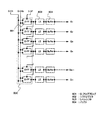
[実施形態1]
図1は、本発明にて交流駆動を行うための画素構成の一実施形態を示している
。
[Embodiment 1]
FIG. 1 shows an embodiment of a pixel configuration for performing AC driving in the present invention.
図1(A)に示すように、各画素はソース信号線(S)101、書込用ゲート信号
線(SEL)102、消去用ゲート信号線(RSE)103、逆方向バイアス用ゲー
ト信号線(RBS)104、第3の手段にあたるスイッチング用TFT105、第
5の手段にあたる消去用TFT106、第4の手段にあたる駆動用TFT107
、第6の手段にあたる逆方向バイアス用TFT108、EL素子109、電流供
給線(VA)111、逆方向バイアス用電源線(VB)112とを有している。EL素
子109の一方の電極(画素電極)は、駆動用TFT107のソース領域もしくは
ドレイン領域のいずれか一方に接続され、他方の電極(対向電極)は、対向電源線
(VC)113に接続されている。
As shown in FIG. 1A, each pixel includes a source signal line (S) 101, a write gate signal line (SEL) 102, an erase gate signal line (RSE) 103, a reverse bias gate signal line ( RBS) 104, switching
, A
(V C ) 113.
図1(A)中、各信号線、電源線に付してある電位は、電源電位もしくは、信号
のLレベル/Hレベルの電位を示す。例えば、ソース信号線101の場合、信号
がLレベルのとき0V、Hレベルのとき7Vである。また、電流供給線111の
電位は6V、逆方向バイアス用電源線112の電位は−14Vである。なお、こ
こに付した電位は一例であり、必ずしもこの電位としなくとも、図1(A)の回路
は動作が可能である。各部のTFTのON、OFFのタイミングと、ゲート・ソ
ース間電圧等を考慮して、適宜決定すれば良い。
In FIG. 1A, the potential attached to each signal line and power supply line indicates the power supply potential or the L level / H level potential of the signal. For example, in the case of the
次に、例としてスイッチング用TFT105、消去用TFT106、逆方向バ
イアス用TFT108がいずれもNチャネル型、駆動用TFT107がPチャネ
ル型、EL素子109において、電流供給線111に接続されている側が陽極、
対向電源線113に接続されている側が陰極である場合の動作について説明する
。
Next, as an example, the switching
The operation when the side connected to the
まず、アドレス(書き込み)期間においては、図1(B)に示すように、書込用ゲ
ート信号線102にパルスが入力され、Hレベル(9V)となり、スイッチング用
TFT105がONし、ソース信号線101に出力されている映像信号が駆動用
TFT107のゲート電極に入力される。ここでは駆動用TFT107がPチャ
ネル型であるため、映像信号がHレベル(7V)のときOFFし、Lレベル(0V)
のときONする。
First, in the address (write) period, as shown in FIG. 1B, a pulse is input to the write
Turns on when.
続いて、サステイン(発光)期間においては、図1(C)に示すように、駆動用TF
T107がONすることによって、電流供給線111の電位(6V)が画素電極に
入力され、対向電源線113の電位(−10V)との電位差によりEL素子109
に順方向バイアスが印加され、EL素子109に電流が流れ発光する。また、駆
動用TFT107がOFFのときは、EL素子109には電流が流れず、非発光
となる。
Subsequently, in the sustain (light emission) period, as shown in FIG.
When T107 is turned ON, the potential (6V) of the
A forward bias is applied to the
続いて、リセット期間においては、図1(D)に示すように、消去用ゲート信号
線103にパルスが入力され、Hレベル(9V)となり、消去用TFT106がO
Nする。消去用TFT106がONすることによって、駆動用TFT107のゲ
ート電極に電流供給線111の電位(6V)が入力され、したがって駆動用TFT
107のゲート・ソース間電圧が0となり、駆動用TFT107がOFFする。
よって、EL素子109は非発光となる。
Subsequently, in the reset period, as shown in FIG. 1D, a pulse is input to the erasing
N. When the erasing
The gate-source voltage of 107 becomes 0, and the driving
Therefore, the
一方、逆方向バイアス期間においては、図1(E)に示すように、逆方向バイア
ス用ゲート信号線104にパルスが入力され、Hレベル(−10V)となり、逆方
向バイアス用TFT108がONする。逆方向バイアス用TFT108がONす
ることによって、画素電極に逆方向バイアス用電源線112の電位(−14V)が
入力される。ここで、逆方向バイアス用電源線112の電位(−14V)を対向電
源線113の電位(−10V)よりも低く設定してあるので、EL素子109には
逆方向バイアスが印加される。逆方向バイアス用ゲート信号線104にHレベル
の電位(−10V)が入力されている間は、EL素子109に逆方向バイアスが印
加され続ける。
On the other hand, in the reverse bias period, as shown in FIG. 1E, a pulse is input to the reverse bias
また、逆方向バイアス用ゲート信号線104にパルス入力が終了し、逆方向バ
イアス用TFT108がOFFしても、EL素子109そのもの、つまりEL素
子109の陽極・陰極間に寄生する容量、もしくは画素電極とある一定電位との
間に設けられた容量によって、画素電極の電荷は保持され、EL素子109には
逆方向バイアスが印加され続ける。
Further, even when the pulse input to the reverse bias
なお、図1に示した構成によると、消去用ゲート信号線と逆方向バイアス用ゲ
ート信号線とは別に設けてあるので、消去期間に対して逆方向バイアス期間を任
意の長さで設定することが出来る。また、逆方向バイアス期間と各ラインの消去
期間とを同じタイミングで設けることによって、ディーティ比を低下させること
なく、交流駆動が可能となる。
According to the configuration shown in FIG. 1, since the erase gate signal line and the reverse bias gate signal line are provided separately, the reverse bias period can be set to an arbitrary length with respect to the erase period. I can do it. Further, by providing the reverse bias period and the erasing period of each line at the same timing, AC driving is possible without reducing the duty ratio.
[実施形態2]
図2は、本発明にて交流駆動を行うための画素構成で、実施形態1とは異なる
一実施形態を示している。
[Embodiment 2]
FIG. 2 shows a pixel configuration for performing AC driving in the present invention, which is an embodiment different from the first embodiment.
図2(A)に示すように、各画素はソース信号線(S)201、書込用ゲート信号
線(SEL)202、消去・逆方向バイアス用ゲート信号線(RSE)203、スイ
ッチング用TFT204、消去用TFT205、駆動用TFT206、逆方向バ
イアス用TFT207、EL素子208、電流供給線(VA)210、逆方向バイ
アス用電源線(VB)211とを有し、EL素子208の一方の電極(画素電極)は
、駆動用TFT206のソース領域もしくはドレイン領域のいずれか一方に接続
され、他方の電極(対向電極)は、対向電源線(VC)212に接続されている。
As shown in FIG. 2A, each pixel includes a source signal line (S) 201, a write gate signal line (SEL) 202, an erase / reverse bias gate signal line (RSE) 203, a switching
図2(A)中、各信号線、電源線に付してある電位は、電源電位もしくは、信号
のLレベル/Hレベルの電位を示す。例えば、ソース信号線201の場合、信号
がLレベルのとき0V、Hレベルのとき7Vである。また、電流供給線210の
電位は6V、逆方向バイアス用電源線211の電位は−14Vである。なお、こ
こに付した電位は一例であり、必ずしもこの電位としなくとも、図2(A)の回路
は動作が可能である。各部のTFTのON、OFFのタイミングと、ゲート・ソ
ース間電圧等を考慮して、適宜決定すれば良い。
In FIG. 2A, the potential attached to each signal line and power supply line indicates the power supply potential or the L level / H level potential of the signal. For example, in the case of the
ここでは、例としてスイッチング用TFT204、消去用TFT205、逆方
向バイアス用TFT207がいずれもNチャネル型、駆動用TFT206がPチ
ャネル型、EL素子208において、電流供給線210に接続されている側が陽
極、対向電源線212に接続されている側が陰極である場合の動作について説明
する。
Here, as an example, the switching
まず、アドレス(書き込み)期間においては、図2(B)に示すように、書込用ゲ
ート信号線202にパルスが入力され、Hレベル(9V)となり、スイッチング用
TFT204がONし、201に出力されている映像信号が駆動用TFT206
のゲート電極に入力される。ここでは駆動用TFT206がPチャネル型である
ため、映像信号がHレベル(7V)のときOFFし、Lレベル(0V)のときONす
る。
First, in the address (write) period, as shown in FIG. 2B, a pulse is input to the write
Are input to the gate electrode. Here, since the driving
続いて、サステイン(発光)期間においては、図2(C)に示すように、駆動用TF
T206がONすることによって、電流供給線210の電位(6V)が画素電極に
入力され、対向電源線212の電位(−10V)との電位差によりEL素子208
に順方向バイアスが印加され、EL素子208に電流が流れ発光する。また、駆
動用TFT206がOFFのときは、EL素子208には電流が流れず、非発光
となる。
Subsequently, in the sustain (light emission) period, as shown in FIG.
When T206 is turned ON, the potential (6V) of the
A forward bias is applied to the
続いて、リセット・逆方向バイアス期間においては、図2(D)に示すように、
消去・逆方向バイアス用ゲート信号線203にパルスが入力され、Hレベル(9
V)となり、消去用TFT205、逆方向バイアス用TFT207がONする。
消去用TFT205がONすることによって、駆動用TFT206のゲート電極
に電流供給線210の電位(6V)が入力され、駆動用TFT206のゲート電極
とソース電極の電位差が0となり、駆動用TFT206がOFFする。
Subsequently, in the reset / reverse bias period, as shown in FIG.
A pulse is input to the
V), and the erasing
When the erasing
同時に、逆方向バイアス用TFT207がONすることによって逆方向バイア
ス用電源線211の電位(−14V)が画素電極に入力される。ここで、逆方向バ
イアス用電源線211の電位(−14V)を対向電源線212の電位(−10V)よ
りも低く設定してあるので、EL素子208には逆方向バイアスが印加される。
消去・逆方向バイアス用ゲート信号線203にHレベルの電位(−10V)が入力
されている間は、EL素子208に逆方向バイアスが印加され続ける。
At the same time, when the reverse bias TFT 207 is turned on, the potential (−14 V) of the reverse bias
While the H-level potential (−10 V) is input to the erase / reverse bias
また、消去・逆方向バイアス用ゲート信号線203にパルス入力が終了し、逆
方向バイアス用TFT207がOFFしても、EL素子208そのものが有する
容量、もしくは画素電極とある一定電位との間に設けられた容量によって、画素
電極の電荷は保持され、EL素子208に逆方向バイアスが印加され続ける。
Further, even when the pulse input to the erase / reverse bias
この時、各ラインの消去期間と逆方向バイアス期間は同一期間となり、高du
ty比を実現出来る。また、消去・逆方向バイアス期間を延長し、任意の長さに
設定するようにしても良い。
At this time, the erase period and the reverse bias period of each line are the same period, and the high du
A ty ratio can be realized. Further, the erase / reverse bias period may be extended and set to an arbitrary length.
[実施形態3]
図3は、本発明にて交流駆動を行うための画素構成で、実施形態1、2とは異
なる一実施形態を示している。
[Embodiment 3]
FIG. 3 shows a pixel configuration for performing AC driving in the present invention, and shows an embodiment different from the first and second embodiments.
図3(A)に示すように、各画素はソース信号線(S)301、書込用ゲート信号
線(SEL)302、消去用ゲート信号線(RSE)303、逆方向バイアス用ゲー
ト信号線(RBS)304、スイッチング用TFT305、駆動用TFT306、
消去用TFT307、逆方向バイアス用TFT308、EL素子309、電流供
給線(VA)311、逆方向バイアス用電源線(VB)312とを有し、EL素子30
9の一方の電極(画素電極)は、駆動用TFT306のソース領域もしくはドレイ
ン領域のいずれか一方に接続され、他方の電極(対向電極)は、対向電源線(VC)
313に接続されている。
As shown in FIG. 3A, each pixel has a source signal line (S) 301, a write gate signal line (SEL) 302, an erase gate signal line (RSE) 303, a reverse bias gate signal line ( RBS) 304, switching
The EL element 30 includes an erasing
One electrode (pixel electrode) 9 is connected to either the source region or the drain region of the driving
313.
図3(A)中、各信号線、電源線に付してある電位は、電源電位もしくは、信号
のLレベル/Hレベルの電位を示す。例えば、ソース信号線301の場合、信号
がLレベルのとき0V、Hレベルのとき7Vである。また、電流供給線311の
電位は6V、逆方向バイアス用電源線312の電位は−14Vである。なお、こ
こに付した電位は一例であり、必ずしもこの電位としなくとも、図3(A)の回路
は動作が可能である。各部のTFTのON、OFFのタイミングと、ゲート・ソ
ース間電圧等を考慮して、適宜決定すれば良い。
In FIG. 3A, the potential attached to each signal line and power supply line indicates the power supply potential or the L level / H level potential of the signal. For example, in the case of the
ここでは、例としてスイッチング用TFT305、逆方向バイアス用TFT3
08がNチャネル型、駆動用TFT306、消去用TFT307がPチャネル型
、EL素子309において、電流供給線311に接続されている側が陽極、対向
電源線313に接続されている側が陰極である場合の動作について説明する。
Here, as an example, switching
In the case where 08 is an N-channel type, driving
まず、アドレス(書き込み)期間においては、図3(B)に示すように、書込用ゲ
ート信号線302にパルスが入力され、Hレベル(9V)となり、スイッチング用
TFT305がONし、ソース信号線301に出力されている映像信号が駆動用
TFT306のゲート電極に入力される。ここでは駆動用TFT306がPチャ
ネル型であるため、映像信号がHレベル(7V)のときOFFし、Lレベル(0V)
のときONする。
First, in the address (write) period, as shown in FIG. 3B, a pulse is input to the write
Turns on when.
また、消去用ゲート信号線303にLレベルの電位(−2V)が入力され、消去
用TFT307がONする。
Further, an L-level potential (−2 V) is input to the erasing
続いて、サステイン(発光)期間においては、図3(C)に示すように、消去用ゲ
ート信号線303に常にLレベルの電位(−2V)が入力され、消去用TFT30
7はONし続ける。更に、駆動用TFT306がONすることによって、電流供
給線311の電位(6V)が画素電極に入力され、対向電源線313の電位(−1
0V)との電位差によりEL素子309に順方向バイアスが印加され、EL素子
309に電流が流れ発光する。また、駆動用TFT306がOFFのときは、E
L素子309に電流は流れず、非発光となる。
Subsequently, in the sustain (light emission) period, as shown in FIG. 3C, the L-level potential (−2 V) is always input to the erase
7 keeps on. Further, when the driving
0V), a forward bias is applied to the EL element 309, and a current flows through the EL element 309 to emit light. When the driving
No current flows through the L element 309 and no light is emitted.
続いて、リセット期間においては、図3(D)に示すように、消去用ゲート信号
線303に常にHレベルの電位(9V)が入力され、消去用TFT307がOFF
し続ける。消去用TFT307がOFFすることによって、電流供給線311か
らEL素子309への電流供給の経路が遮断され、EL素子309は非発光とな
る。実施形態1、2の場合と異なり、ここでは消去用TFT307は、発光期間
を通じてONし続け、消去期間を通じてOFFし続けている。
Subsequently, in the reset period, as shown in FIG. 3D, an H-level potential (9 V) is always input to the erasing
Keep doing. When the erasing
一方、逆方向バイアス期間においては、図3(E)に示すように、逆方向バイア
ス用ゲート信号線304にパルスが入力され、Hレベル(−10V)となり、逆方
向バイアス用TFT308がONする。逆方向バイアス用TFT308がONす
ることによって、画素電極に逆方向バイアス用電源線312の電位(−14V)が
入力される。ここで、逆方向バイアス用電源線312の電位(−14V)を対向電
源線313の電位(−10V)よりも低く設定してあるので、EL素子には逆方向
バイアスが印加される。逆方向バイアス用ゲート信号線304にHレベルの電位
(−10V)が入力されている間は、EL素子309に逆方向バイアスが印加され
続ける。
On the other hand, in the reverse bias period, as shown in FIG. 3E, a pulse is input to the reverse bias
While (−10 V) is input, the reverse bias is continuously applied to the EL element 309.
また、逆方向バイアス用ゲート信号線304にパルス入力が終了し、逆方向バ
イアス用TFT308がOFFしても、EL素子309そのものが有する容量、
もしくは画素電極とある一定電位との間に設けられた容量によって、画素電極の
電荷は保持され、EL素子309には逆方向バイアスが印加され続ける。
Further, even when the pulse input to the reverse bias
Alternatively, the electric charge of the pixel electrode is held by a capacitor provided between the pixel electrode and a certain potential, and a reverse bias is continuously applied to the EL element 309.
消去期間中、消去用TFT307は常にOFFさせる必要があり、逆方向バイ
アス期間図と各ラインの消去期間とを重ねることができ、高duty比が実現出
来る。また、逆方向バイアス期間を任意の長さに設定することが出来る。
During the erasing period, it is necessary to always turn off the erasing
[実施形態4]
図4は、本発明にて交流駆動を行うための画素構成で、実施形態1〜3とは異
なる一実施形態を示している。
[Embodiment 4]
FIG. 4 shows a pixel configuration for performing AC driving in the present invention, which is an embodiment different from the first to third embodiments.
図4(A)に示すように、各画素はソース信号線(S)401、書込用ゲート信号
線(SEL)402、消去・逆方向バイアス用ゲート信号線(RSE)403、スイ
ッチング用TFT404、駆動用TFT405、消去用TFT406、逆方向バ
イアス用TFT407、EL素子408、電流供給線(VA)410、逆方向バイ
アス用電源線(VB)411とを有し、EL素子408の一方の電極(画素電極)は
、駆動用TFT405のソース領域もしくはドレイン領域のいずれか一方に接続
され、他方の電極(対向電極)は、対向電源線(VC)412に接続されている。
As shown in FIG. 4A, each pixel includes a source signal line (S) 401, a write gate signal line (SEL) 402, an erase / reverse bias gate signal line (RSE) 403, a switching
図4(A)中、各信号線、電源線に付してある電位は、電源電位もしくは、信号
のLレベル/Hレベルの電位を示す。例えば、ソース信号線401の場合、信号
がLレベルのとき0V、Hレベルのとき7Vである。また、電流供給線410の
電位は6V、逆方向バイアス用電源線411の電位は−14Vである。なお、こ
こに付した電位は一例であり、必ずしもこの電位としなくとも、図4(A)の回路
は動作が可能である。各部のTFTのON、OFFのタイミングと、ゲート・ソ
ース間電圧等を考慮して、適宜決定すれば良い。
In FIG. 4A, the potential attached to each signal line and power supply line indicates the power supply potential or the L level / H level potential of the signal. For example, in the case of the
ここでは、スイッチング用TFT404、逆方向バイアス用TFT407がN
チャネル型、駆動用TFT405、消去用TFT406がPチャネル型、電流供
給線410を陽極電位、対向電源線412を陰極電位とした場合の駆動について
説明する。EL素子408において、電流供給線410に接続されている側が陽
極、対向電源線412に接続されている側が陰極である場合の動作について説明
する。
Here, the switching
A description will be given of driving when the channel type, driving
まず、アドレス(書き込み)期間においては、図4(B)に示すように、書込用ゲ
ート信号線402にパルスが入力され、Hレベル(9V)となり、スイッチング用
TFT404がONし、401に出力されている映像信号が駆動用TFT405
のゲート電極に入力される。ここでは駆動用TFT405がPチャネル型である
ため、映像信号がHレベル(7V)のときOFFし、Lレベル(0V)のときONす
る。
First, in the address (write) period, as shown in FIG. 4B, a pulse is input to the write
Are input to the gate electrode. Here, since the driving
また、消去・逆方向バイアス用ゲート信号線403にLレベルの電位(−16V)
が入力され、消去用TFT406がONし、逆方向バイアス用TFT407がO
FFする。
The erase / reverse bias
Is input, the erasing
FF.
続いて、サステイン(発光)期間においては、図4(C)に示すように、消去・逆
方向バイアス用ゲート信号線403に常にLレベルの電位(−16V)が入力され
、消去用TFT406はONし続け、逆方向バイアス用TFT407はOFFし
続ける。
Subsequently, in the sustain (light emission) period, as shown in FIG. 4C, an L-level potential (−16 V) is always input to the erase / reverse bias
更に、駆動用TFT405がONすることによって、電流供給線410の電位
(6V)が画素電極に入力され、対向電源線412の電位(−10V)との電位差に
よりEL素子408に順方向バイアスが印加され、EL素子408に電流が流れ
発光する。また、駆動用TFT405がOFFのときは、EL素子408には電
流が流れず、非発光となる。
Further, when the driving
(6V) is input to the pixel electrode, a forward bias is applied to the
続いて、リセット・逆方向バイアス期間においては、図4(D)に示すように、
消去・逆方向バイアス用ゲート信号線403に常にHレベルの電位(9V)が入力
され、消去用TFT406がOFFし、逆方向バイアス用TFT407がONす
る。この動作により、逆方向バイアス用電源線の電位(−14V)が画素電極に入
力される。ここで、逆方向バイアス用電源線411の電位(−14V)を対向電源
線412の電位(−10V)よりも低く設定してあるので、EL素子408には逆
方向バイアスが印加される。消去・逆方向バイアス用ゲート信号線403にHレ
ベルの電位(9V)が入力されている間は、消去用TFT406がOFFし続ける
ことによって電流供給線410からEL素子408への電流供給経路が遮断され
、EL素子408は非発光となり、逆方向バイアス用TFT407がONし続け
ることによってEL素子408に逆方向バイアスが印加され続ける。
Subsequently, in the reset / reverse bias period, as shown in FIG.
An H-level potential (9 V) is always input to the erase / reverse bias
この時、各ラインの消去期間と逆方向バイアス期間は同一期間となり、高du
ty比が実現出来る。また、消去・逆方向バイアス期間を延長し、任意の長さに
設定することが出来る。
At this time, the erase period and the reverse bias period of each line are the same period, and the high du
A ty ratio can be realized. In addition, the erase / reverse bias period can be extended and set to an arbitrary length.
実施形態1〜4の通り、各画素に逆方向バイアス用電源線を設けることで、カ
ラー表示の発光装置において、R、G、BそれぞれのEL素子に合わせた任意の
値の逆方向バイアスを印加することが出来る。
As in
また、R、G、Bの中で最も高い逆方向バイアスを印加する際の電位に合わせ
て逆方向バイアス用電源線の電位を共通化し、隣接する画素で逆方向バイアス用
電源線を共用しても良い。この場合、配線数を減らすことが出来、高開口率が期
待出来る。
Further, the potential of the reverse bias power line is made common to the potential when the highest reverse bias is applied among R, G, and B, and the reverse bias power line is shared by adjacent pixels. Also good. In this case, the number of wirings can be reduced and a high aperture ratio can be expected.
また、実施形態1〜4では、駆動用TFTを線形領域で動作させた場合、すな
わち定電圧駆動方式を例にとって説明しているが、EL素子の寿命を考慮した場
合、駆動用TFTを飽和領域で動作させ、EL素子に一定の電流を供給すること
の出来る定電流駆動を行うことが望ましい。
In the first to fourth embodiments, the case where the driving TFT is operated in the linear region, that is, the constant voltage driving method is described as an example. However, when the lifetime of the EL element is considered, the driving TFT is set in the saturation region. It is desirable to perform constant current driving that can supply a constant current to the EL element.
以下に、本発明の実施例について記載する。 Examples of the present invention will be described below.
図12に示すように、携帯電話等の電子機器の表示部として発光装置が使用され
る場合は、発光装置1201という形で内蔵される。ここで、発光装置1201
とは、パネルと、パネルを駆動するための信号処理用LSI、メモリ等を実装し
た基板とを接続した形態を指す。
As shown in FIG. 12, when a light emitting device is used as a display unit of an electronic device such as a mobile phone, the
The term “panel” refers to a configuration in which a panel and a substrate on which a signal processing LSI, a memory, and the like for driving the panel are mounted are connected.
発光装置1201をブロック図として、図6(A)に示す。発光装置1201は
、パネル650、駆動回路660を有する。
A block diagram of the light-emitting
駆動回路660は信号生成部611、電源部612を有する。電源部612は
、外部バッテリーより供給される電源より、ソース信号線駆動回路、ゲート信号
線駆動回路、発光素子、信号生成部611等に、それぞれ所望の複数の電圧値の
電源を生成し、供給する。信号生成部611には、電源、映像信号、同期信号が
入力され、発光装置650にて処理が出来るように、各種信号の変換を行う他、
ソース信号線駆動回路、ゲート信号線駆動回路を駆動するためのクロック信号等
を生成する。
The drive circuit 660 includes a signal generation unit 611 and a power supply unit 612. The power supply unit 612 generates and supplies power with a plurality of desired voltage values to the source signal line drive circuit, the gate signal line drive circuit, the light emitting element, the signal generation unit 611, and the like from the power supplied from the external battery. To do. The signal generator 611 receives a power source, a video signal, and a synchronization signal, and converts various signals so that the light emitting device 650 can perform processing.
A clock signal and the like for driving the source signal line driver circuit and the gate signal line driver circuit are generated.
また、パネル650は基板上に、画素部601、ソース信号線駆動回路602
、書込用ゲート信号線駆動回路603、消去用ゲート信号線駆動回路604、逆
方向バイアス用ゲート信号線駆動回路605、FPC606等を配置することに
よって構成される。
The panel 650 includes a pixel portion 601 and a source signal line driver circuit 602 over a substrate.
, A write gate signal line drive circuit 603, an erase gate signal line drive circuit 604, a reverse bias gate signal line drive circuit 605, an
基板中央部には、画素部601が配置され、その周辺部には、ソース信号線駆
動回路602、書込用ゲート信号線駆動回路603、消去用ゲート信号線駆動回
路604、逆方向バイアス用ゲート信号線駆動回路605等が配置されている。
EL素子の対向電極は、画素部601全体面に形成されており、FPC606を
通じて、対向電位が与えられる。ソース信号線駆動回路602、書込用ゲート信
号線駆動回路603、消去用ゲート信号線駆動回路604、逆方向バイアス用ゲ
ート信号線駆動回路605を駆動するための信号、及び電源の供給はFPC60
6を通じて、駆動回路660より行われる。
A pixel portion 601 is disposed in the central portion of the substrate, and a source signal line driving circuit 602, a writing gate signal line driving circuit 603, an erasing gate signal line driving circuit 604, and a reverse bias gate are provided in the periphery thereof. A signal line driver circuit 605 and the like are arranged.
The counter electrode of the EL element is formed on the entire surface of the pixel portion 601, and a counter potential is applied through the
6 from the drive circuit 660.
また、図6(B)に示すように、消去期間と逆方向バイアス期間を同じタイミン
グに設ける場合等は、消去・逆方向バイアス用ゲート信号線駆動回路607と、
同一駆動回路を使用することができ、狭額縁化が可能である。
Further, as shown in FIG. 6B, when the erase period and the reverse bias period are provided at the same timing, the erase / reverse bias gate signal line drive circuit 607,
The same drive circuit can be used, and the frame can be narrowed.
本実施例にて示した発光装置1201は、パネル650と、信号生成部611
および電源部612を含む駆動回路660とは独立して作成されているが、これ
らを基板上に一体形成して作製しても良い。
A
In addition, the driving circuit 660 including the power supply unit 612 is formed independently, but these may be formed integrally on a substrate.
デジタル映像信号を用いて映像の表示を行う場合の、ソース信号線駆動回路の
概略図を図7に、ゲート信号線駆動回路の概略図を図8に示す。
FIG. 7 shows a schematic diagram of a source signal line driver circuit and FIG. 8 shows a schematic diagram of a gate signal line driver circuit when displaying a video using a digital video signal.
ソース信号線駆動回路は、D−フリップフロップ701を複数段用いてなるシ
フトレジスタ702、第1のラッチ回路703a、第2のラッチ回路703b、
レベルシフタ704、バッファ705等を有する。外部より入力される信号は、
クロック信号(S−CK)、反転クロック信号(S−CKb)、スタートパルス(S
−SP)、デジタル映像信号(Digital Video Data)である。図7のような構成の
場合、デジタル映像信号は、例えば「最上位ビットの1行目→2行目→・・・最
終行、→第2ビットの1行目→2行目→・・・最終行、→・・・最下位ビットの
1行目→2行目→・・・最終行」というように、直列に入力される。
The source signal line driver circuit includes a
A
Clock signal (S-CK), inverted clock signal (S-CKb), start pulse (S
-SP), a digital video signal. In the case of the configuration as shown in FIG. 7, the digital video signal is, for example, “the first row of the most significant bit → the second row →... The last row, the first row of the second bit → the second row →. The last row,..., The first row of the least significant bit, the second row, and the last row are input in series.
まず、クロック信号、クロック反転信号、およびスタートパルスのタイミング
に従って、シフトレジスタ702より、順次サンプリングパルスが出力される。
続いて、サンプリングパルスは、第1のラッチ回路703aに入力され、サンプ
リングパルスが入力されたタイミングで、ビット毎のデジタル映像信号を取り込
み、保持する。この動作が、1列目から順に行われる。
First, sampling pulses are sequentially output from the
Subsequently, the sampling pulse is input to the
最終段の第1のラッチ回路703aにおいてデジタル映像信号の保持が完了す
ると、水平帰線期間中にラッチパルスが入力され、このタイミングで、第1のラ
ッチ回路703aにおいて保持されているデジタル映像信号は、一斉に第2のラ
ッチ回路703bへと転送される。その後、レベルシフタにおいてパルスの振幅
変換を受け、続いて、バッファにおいて映像信号波形が整形された後、それぞれ
のソース信号線S1〜Sxへと出力される。
When the holding of the digital video signal is completed in the
一方、ゲート信号線駆動回路は、D−フリップフロップ801を複数段用いて
なるシフトレジスタ802、レベルシフタ803、バッファ804等を有する。
外部より入力される信号は、クロック信号(G−CK)、反転クロック信号(G−
CKb)、スタートパルス(G−SP)である。
On the other hand, the gate signal line driver circuit includes a
Signals input from the outside are the clock signal (G-CK) and the inverted clock signal (G-
CKb) and a start pulse (G-SP).
まず、クロック信号、クロック反転信号、およびスタートパルスのタイミング
に従って、シフトレジスタ802より、順次パルスが出力される。続いて、レベ
ルシフタ803によってパルスの振幅変換を受け、続いて、バッファにおいてパ
ルス波形が整形された後、ゲート信号線G1〜Gyを順次選択するパルスとして
、それぞれのゲート信号線へと出力される。最終行Gyでの選択が終了すると、
垂直帰線期間を経たあと、再びシフトレジスタ802よりパルスが出力され、順
にゲート信号線の選択を行う。
First, pulses are sequentially output from the
After the vertical blanking period, a pulse is output again from the
また、実施形態1、3を採用し、消去用ゲート信号線と逆方向バイアス用ゲー
ト信号線に全く同じタイミングのパルスを入力する場合、図9に示すような方法
で、消去用ゲート信号線駆動回路と逆方向バイアス用ゲート信号線駆動回路を同
一にすることができ、狭額縁化が可能である。
Further, when the first and third embodiments are adopted and pulses having exactly the same timing are input to the erase gate signal line and the reverse bias gate signal line, the erase gate signal line is driven by the method shown in FIG. The circuit and the reverse bias gate signal line driving circuit can be made the same, and the frame can be narrowed.
図9のゲート信号線駆動回路は、D−フリップフロップ901を複数段用いて
なるシフトレジスタ902、レベルシフタ903、バッファ904、電圧変換回
路905等を有する。外部より入力される信号は、クロック信号(G−CK)、反
転クロック信号(G−CKb)、スタートパルス(G−SP)である。
9 includes a
動作は前述したゲート信号線駆動回路とほぼ同様である。シフトレジスタ90
2から順次出力されるパルスは、レベルシフタ903による振幅変換、また、バ
ッファ904によってパルス波形の成形を受けた後、そのまま消去用ゲート信号
線G1〜Gyに出力されるものと、電圧変換回路905に入力されるものとに分
かれる。後者は、電圧変換回路905によって、所望の振幅(VH−VL間)を有す
るパルスに変換され、逆方向バイアス用ゲート信号線Gb1〜Gbyに出力され
る。また、電圧変換回路905は消去用ゲート信号線G1〜Gyの側に設けられ
ていても良い。
The operation is almost the same as that of the gate signal line driving circuit described above. Shift register 90
The pulses sequentially output from 2 are subjected to amplitude conversion by the
実施形態に挙げた画素構成をSES駆動し、逆方向バイアスを印加させる場合
の実際の動作タイミングについて、図10、図11を用いて説明する。
The actual operation timing when the pixel configuration described in the embodiment is SES-driven and a reverse bias is applied will be described with reference to FIGS.
まず、通常のSES駆動について、図11を用いて説明する。 First, normal SES driving will be described with reference to FIG.
1フレーム期間は、複数のサブフレーム期間に分割される。ここでは一例とし
て、6つのサブフレーム期間SF1〜SF6に分割している。各サブフレーム期
間は、アドレス(書き込み)期間Taと、サステイン(発光)期間Tsとを有する。
各サブフレーム期間のサステイン(発光)期間は、それぞれの長さが異なっており
、どのサブフレームにおいてEL素子を発光させるかによって、1フレーム期間
あたりの各画素の発光時間が決定し、この長短によって階調表示を行う。
One frame period is divided into a plurality of subframe periods. Here, as an example, it is divided into six subframe periods SF1 to SF6. Each subframe period includes an address (writing) period Ta and a sustain (light emission) period Ts.
The sustain (light emission) period of each subframe period is different in length, and the light emission time of each pixel per frame period is determined depending on which subframe the EL element emits light. Perform gradation display.
ここで、サブフレーム期間の分割数が多いほど、多階調の表示が可能となるが
、一部のサブフレーム期間においては、サステイン(発光)期間がアドレス(書き
込み)期間よりも短くなるものが現れる。この場合、異なるサブフレーム期間が
有するアドレス(書き込み)期間が重複することは出来ないため、さらにリセット
期間Trと、消去期間Teとを有する。
Here, as the number of subframe periods is increased, multi-grayscale display is possible, but in some subframe periods, the sustain (light emission) period is shorter than the address (write) period. appear. In this case, since the address (write) periods included in different subframe periods cannot be overlapped, a reset period Tr and an erase period Te are further provided.
リセット期間TrとはEL素子を強制的に非発光状態にする信号を画素に入力
する期間であり、消去期間Trとはリセット期間に入力された信号に基づいて、
EL素子の非発光状態が続いている期間である。
The reset period Tr is a period during which a signal for forcibly turning off the EL element is input to the pixel, and the erase period Tr is based on the signal input during the reset period.
This is a period during which the non-light emitting state of the EL element continues.
動作としては、まずSF1のアドレス(書き込み)期間Ta1において、1行目
から順に書込用ゲート信号線にパルスが入力され、ソース信号線に出力されてい
るデジタル映像信号を書き込んでいく。デジタル映像信号が書き込まれた行にお
いては直ちにサステイン(発光)期間Ts1へと移る。1行目〜最終行まで書込作
業が完了するとアドレス(書き込み)期間Ta1は終了する。次にサステイン(発
光)期間Ta1が終了した1行目より、書込用ゲート信号線にパルスが入力され
、SF2のアドレス(書き込み)期間Ta2が開始される。
As an operation, first, in the address (write) period Ta1 of SF1, pulses are input to the write gate signal line in order from the first row, and the digital video signal output to the source signal line is written. In the row where the digital video signal is written, the operation immediately proceeds to the sustain (light emission) period Ts1. When the writing operation is completed from the first line to the last line, the address (writing) period Ta1 ends. Next, from the first row where the sustain (light emission) period Ta1 ends, a pulse is input to the write gate signal line, and an address (write) period Ta2 of SF2 is started.
上述の動作を繰り返し、SF2、SF3が終了し、SF4のアドレス(書き込
み)期間Ta4が開始される。ここで、アドレス(書き込み)期間Ta4はサステ
イン(発光)期間Ts4よりも長いため、サステイン(発光)期間Ts4の終了後直
ちに次のアドレス(書き込み)期間Ta5を開始することが出来ない。よって、サ
ステイン(発光)期間Ts4が終了した1行目より、リセット期間Tr4が開始さ
れる。このときの消去期間Te4の長さは、通常、図11(A)のように1行目の
サステイン(発光)期間が終了した後から、最終行のアドレス(書き込み)期間が終
了するまでの長さとなる。
The above operation is repeated, SF2 and SF3 are finished, and an address (write) period Ta4 of SF4 is started. Here, since the address (write) period Ta4 is longer than the sustain (light emission) period Ts4, the next address (write) period Ta5 cannot be started immediately after the end of the sustain (light emission) period Ts4. Therefore, the reset period Tr4 is started from the first row where the sustain (light emission) period Ts4 ends. The length of the erase period Te4 at this time is usually the length from the end of the sustain (light emission) period of the first row to the end of the address (write) period of the last row as shown in FIG. It becomes.
続いて、SF5のアドレス(書き込み)期間Ta5が開始される。SF5、SF
6が終了すると1フレーム期間が終了し、次のフレーム期間となる。
Subsequently, the address (write) period Ta5 of SF5 is started. SF5, SF
When 6 is completed, one frame period ends and the next frame period is reached.
続いて、実施形態1〜4に示した回路における動作タイミングについて、図1
0を用いて説明する。
Next, the operation timing in the circuits shown in
This will be described using 0.
1フレーム期間を6つのサブフレーム期間SF1〜SF6に分割している。各サ
ブフレームはアドレス(書き込み)期間Ta、サステイン(発光)期間Tsを有する
。また、アドレス(書き込み)期間Taがサステイン(発光)期間Tsよりも長いサ
ブフレーム(ここではSF4、SF5、SF6が該当する)はアドレス(書き込み)
期間Ta、サステイン(発光)期間Tsの他に、リセット期間Tr、消去期間Te
、逆方向バイアス期間Tb、逆方向バイアス印加期間Tiを有する。
One frame period is divided into six subframe periods SF1 to SF6. Each sub-frame has an address (writing) period Ta and a sustain (light emission) period Ts. In addition, subframes (here, SF4, SF5, and SF6 correspond) in which the address (write) period Ta is longer than the sustain (light emission) period Ts are address (write).
In addition to the period Ta and the sustain (light emission) period Ts, the reset period Tr and the erase period Te
, A reverse bias period Tb and a reverse bias application period Ti.
アドレス(書き込み)期間Taとは画素にデジタル映像信号を書き込む期間であり
、サステイン(発光)期間Tsとはアドレス(書き込み)期間において、書き込まれ
たデジタル映像信号に基づいて、EL素子が発光、または非発光状態をとる期間
である。どのサブフレーム期間でEL素子が発光するかによって、1フレーム期
間あたりの各画素の発光時間が決まり、この長短によって階調表示を行う。
The address (writing) period Ta is a period in which a digital video signal is written to the pixel, and the sustain (light emission) period Ts is an EL element that emits light based on the written digital video signal in the address (writing) period, or This is a period in which a non-light emitting state is taken. The light emission time of each pixel per frame period is determined depending on which subframe period the EL element emits light, and gradation display is performed based on this length.
リセット期間TrとはEL素子を強制的に非発光状態にする信号を画素に入力
する期間であり、消去期間Trとはリセット期間に入力された信号に基づいて、
ELの非発光状態が続いている期間である。また、逆方向バイアス期間Tbとは
、EL素子に逆方向バイアスを印加するための信号を画素に入力する期間であり
、逆方向バイアス印加期間Tiとは逆方向バイアス期間Tbに入力された信号に
基づいて、EL素子に逆方向バイアスが印加されている状態が続いている期間で
ある。
The reset period Tr is a period during which a signal for forcibly turning off the EL element is input to the pixel, and the erase period Tr is based on the signal input during the reset period.
This is a period during which the non-light emitting state of EL continues. The reverse bias period Tb is a period during which a signal for applying a reverse bias to the EL element is input to the pixel, and the reverse bias application period Ti is a signal input during the reverse bias period Tb. Based on this, this is a period in which the reverse bias is applied to the EL element.
動作としては、まずSF1のアドレス(書き込み)期間Ta1において、1行目か
ら順に書込用ゲート信号線にパルスが入力され、ソース信号線に出力されている
デジタル映像信号を書き込んでいく。デジタル映像信号が書き込まれた行におい
ては直ちにサステイン(発光)期間Ts1へと移る。1行目〜最終行まで書込作業
が完了するとアドレス(書き込み)期間Ta1は終了する。次にサステイン(発光)
期間Ta1が終了した1行目より、書込用ゲート信号線にパルスが入力され、S
F2のアドレス(書き込み)期間Ta2が開始される。
As an operation, first, in the address (write) period Ta1 of SF1, pulses are input to the write gate signal line in order from the first row, and the digital video signal output to the source signal line is written. In the row where the digital video signal is written, the operation immediately proceeds to the sustain (light emission) period Ts1. When the writing operation is completed from the first line to the last line, the address (writing) period Ta1 ends. Next, sustain (emission)
From the first row where the period Ta1 ends, a pulse is input to the write gate signal line, and S
The address (write) period Ta2 of F2 is started.
上述の動作を繰り返し、SF2、SF3が終了し、SF4のアドレス(書き込み)
期間Ta4が開始される。ここで、アドレス(書き込み)期間Ta4はサステイン
(発光)期間Ts4よりも長いため、サステイン(発光)期間Ts4の終了後直ちに
次のアドレス(書き込み)期間Ta5を開始することが出来ない。よって、サステ
イン(発光)期間Ts4が終了した1行目より、リセット期間Tr4が開始される
。このときの消去期間Te4の長さは、通常、図10(A)のように1行目のサス
テイン(発光)期間が終了した後から、最終行のアドレス(書き込み)期間が終了す
るまでの長さとなる。
The above operation is repeated, SF2 and SF3 are completed, and the address of SF4 (writing)
Period Ta4 is started. Here, the address (write) period Ta4 is the sustain period.
Since it is longer than the (light emission) period Ts4, the next address (writing) period Ta5 cannot be started immediately after the end of the sustain (light emission) period Ts4. Therefore, the reset period Tr4 is started from the first row where the sustain (light emission) period Ts4 ends. The length of the erasing period Te4 at this time is usually the length from the end of the sustain (light emission) period of the first row until the end of the address (writing) period of the last row as shown in FIG. It becomes.
このとき、リセット期間Tr4と同時に逆方向バイアス期間Tb4が開始されて
いて、消去期間Te4と逆方向バイアス印加期間が同時となり、各行ごとに逆方
向バイアスが印加されていく。続いて、SF5のアドレス(書き込み)期間Ta5
が開始される。SF5、SF6が終了すると1フレーム期間が終了し、次のフレ
ーム期間となる。
At this time, the reverse bias period Tb4 is started at the same time as the reset period Tr4, the erase period Te4 and the reverse bias application period are simultaneous, and the reverse bias is applied to each row. Subsequently, the address (write) period Ta5 of SF5
Is started. When SF5 and SF6 are finished, one frame period is finished and the next frame period is reached.
図10(B)で示すように、消去・逆方向バイアス印加期間Tei4、Tei5、
Tei6を任意の長さに延長し、EL素子に逆方向バイアスが印加される時間を
調整することも可能である。
As shown in FIG. 10B, the erase / reverse bias application period Tei4, Tei5,
It is also possible to adjust the time during which the reverse bias is applied to the EL element by extending Tei6 to an arbitrary length.
更に、実施形態1、3を採用した場合には、図10(C)で示すように、リセット
期間Tr4と逆方向バイアス期間Tb4を独立させることができ、逆方向バイア
ス印加期間Ti4は消去期間Te4に含まれ、且つ、隣り合う逆方向バイアス期
間Tbが重ならない範囲で任意に設定でき、EL素子に逆方向バイアスが印加さ
れる時間を調整することも可能である。
Further, when the first and third embodiments are adopted, as shown in FIG. 10C, the reset period Tr4 and the reverse bias period Tb4 can be made independent, and the reverse bias application period Ti4 is the erase period Te4. And the reverse bias period Tb adjacent to each other can be arbitrarily set, and the time during which the reverse bias is applied to the EL element can be adjusted.
また、ここではアドレス(書き込み)期間Taがサステイン(発光)期間Tsより
も長いサブフレームのみがリセット期間Tr、消去期間Te、逆方向バイアス期
間Tb、逆方向バイアス印加期間Tiを有する場合を説明したが、アドレス(書
き込み)期間Taがサステイン(発光)期間Tsよりも短い、または同じ長さのサ
ブフレーム期間に各期間を設け、EL素子に逆方向バイアスを印加することも可
能である。
Further, here, the case where only the subframe in which the address (write) period Ta is longer than the sustain (light emission) period Ts has the reset period Tr, the erase period Te, the reverse bias period Tb, and the reverse bias application period Ti has been described. However, the address (write) period Ta is shorter than the sustain (light emission) period Ts, or each period is provided in a subframe period having the same length, and a reverse bias can be applied to the EL element.
また、表示階調数を増やしたい場合は、サブフレーム期間の分割数を増やせば
良いし、サブフレーム期間の順序は必ずしも上位ビット→下位ビットといった順
序である必要はなく、1フレーム期間中、ランダムに並んでいても良い。
In addition, when it is desired to increase the number of display gradations, the number of subframe periods may be increased, and the order of subframe periods does not necessarily have to be the order of upper bits → lower bits, and is random during one frame period. You may line up.
図5(A)に、実施形態1にて示した図1の構成を有する画素を実際に作製した
場合の素子レイアウト例を示す。また、図5(A)において、X−X'で示される
部分の断面図を図5(B)に示す。
FIG. 5A shows an example of an element layout in the case where a pixel having the configuration of FIG. 1 shown in
図5(B)において、500は絶縁表面を有する基板である。基板500上には
、駆動用TFT507等が設けられ、駆動用TFT507のソース・ドレイン領
域を形成する不純物領域に接続されるように、配線材料でなるソース・ドレイン
電極が形成され、そのうちの一方と、画素電極509が、重なり合う部分で接続
するように設けられている。画素電極509上には、有機導電体膜522が設け
られ、さらに有機薄膜(発光層)523が設けられている。有機薄膜(発光層)52
3上には、対向電極524が設けられている。対向電極524は、全ての画素で
共通に接続されるように、ベタ付けの形で形成される。
In FIG. 5B,
3 is provided with a
うち、本文中でEL素子と表記しているものは、図5(B)において、画素電極
509、有機導電体膜522、有機薄膜(発光層)523、対向電極524の積層
体に相当し、画素電極509と対向電極524のうちいずれか一方が陽極、他方
が陰極となる。
Among them, what is described as an EL element in the text corresponds to a stacked body of a
有機薄膜(発光層)523から発せられた光は、画素電極509もしくは対向電
極524のうちいずれかを透過して発せられる。このとき、図5(B)において、
画素電極側、すなわちTFT等が形成されている側に光が発せられる場合を下面
出射、対向電極側に光が発せられる場合を上面出射と呼ぶ。
Light emitted from the organic thin film (light emitting layer) 523 is emitted through either the
The case where light is emitted to the pixel electrode side, that is, the side where the TFT or the like is formed is called bottom emission, and the case where light is emitted to the counter electrode side is called top emission.
下面出射の場合、画素電極509を透明導電膜によって形成される。逆に、上
面出射の場合、対向電極524を透明導電膜によって形成される。
In the case of bottom emission, the
なお、本実施例にて示した構成はあくまで一例であり、画素レイアウト、断面
構成、EL素子の電極の積層順等に関してはこの限りではない。
Note that the structure shown in this embodiment is merely an example, and the pixel layout, the cross-sectional structure, the stacking order of the electrodes of the EL element, and the like are not limited thereto.
また、カラー表示の発光装置においては、R・G・Bそれぞれの発光色を持つ
EL素子を塗りわけても良いし、単色のEL素子をベタ付けの形で塗り、カラー
フィルタによってR・G・Bの発光を得るようにしても良い。
In a light emitting device for color display, EL elements having emission colors of R, G, and B may be separately applied, or a monochrome EL element may be applied in a solid form, and R, G, and B may be applied by a color filter. You may make it obtain light emission.
本実施例においては、発光層として高分子化合物を適用し、さらに陽極と発光
層との間に導電性高分子化合物からなるバッファ層を設けた発光素子において、
直流駆動(常に順方向バイアスを印加)と交流駆動(順方向バイアスと逆方向バイ
アスを一定周期で交互に印加)を行った際の輝度劣化について測定を行った結果
について述べる。
In this example, in a light emitting device in which a polymer compound is applied as a light emitting layer and a buffer layer made of a conductive polymer compound is provided between the anode and the light emitting layer,
The following describes the results of measurement of luminance degradation during direct current drive (always forward bias applied) and alternating current drive (forward bias and reverse bias applied alternately at fixed intervals).
図14(A)(B)は、順方向バイアス:3.7V、逆方向バイアス:1.7V、
デューティ50%、交流周波数60Hzにおいて交流駆動を行った際の信頼性試
験の結果を示している。初期輝度は約400cd/cm2であった。比較用に、直流駆
動(順方向バイアス:3.65V)を行った際の信頼性試験の結果も同時に示した
。結果、直流駆動においては、400時間程度で輝度が半減したのに対し、交流
駆動においては、約700時間経過後も、半減には至らなかった。
14A and 14B show a forward bias: 3.7 V, a reverse bias: 1.7 V,
The result of the reliability test at the time of performing an alternating current drive in 50% duty and 60 Hz alternating frequency is shown. The initial luminance was about 400 cd / cm 2 . For comparison, the results of a reliability test when DC driving (forward bias: 3.65 V) was performed are also shown. As a result, in the direct current drive, the luminance was reduced by half in about 400 hours, whereas in the alternating current drive, even after about 700 hours, the brightness was not reduced to half.
図14(C)(D)は、順方向バイアス:3.8V、逆方向バイアス:1.7V、
デューティ50%、交流周波数600Hzにおいて交流駆動を行った際の信頼性
試験の結果を示している。初期輝度は約300cd/cm2であった。比較用に、直流
駆動(順方向バイアス:3.65V)を行ったさいの信頼性試験の結果も同時に示
した。結果、直流駆動においては、500時間程度で輝度が半減したのに対し、
交流駆動においては、約700時間経過後も、初期輝度の60%程度を保持して
いた。
14C and 14D show the forward bias: 3.8V, the reverse bias: 1.7V,
The result of the reliability test at the time of performing an alternating current drive in 50% duty and 600 Hz alternating frequency is shown. The initial luminance was about 300 cd / cm 2 . For comparison, the results of a reliability test when DC driving (forward bias: 3.65 V) was performed are also shown. As a result, in direct current drive, the brightness was halved in about 500 hours,
In AC driving, about 60% of the initial luminance was maintained after about 700 hours.
発光素子を用いた発光装置は自発光型であるため、液晶ディスプレイに比べ、
明るい場所での視認性に優れ、視野角が広い。従って、様々な電子機器の表示部
に用いることが出来る。
Since the light-emitting device using a light-emitting element is a self-luminous type, compared to a liquid crystal display,
Excellent visibility in bright places and wide viewing angle. Therefore, it can be used for display portions of various electronic devices.
本発明の発光装置を用いた電子機器として、ビデオカメラ、デジタルカメラ、
ゴーグル型ディスプレイ(ヘッドマウントディスプレイ)、ナビゲーションシステ
ム、音響再生装置(カーオーディオ、オーディオコンポ等)、ノート型パーソナル
コンピュータ、ゲーム機器、携帯情報端末(モバイルコンピュータ、携帯電話、
携帯型ゲーム機または電子書籍等)、記録媒体を備えた画像再生装置(具体的には
Digital Versatile Disc(DVD)等の記録媒体を再生し、その画像を表示しうる
ディスプレイを備えた装置)などが挙げられる。特に、斜め方向から画面を見る
機会が多い携帯情報端末は、視野角の広さが重要視されるため、発光装置を用い
ることが望ましい。それら電子機器の具体例を図13に示す。
As an electronic device using the light emitting device of the present invention, a video camera, a digital camera,
Goggle type display (head mounted display), navigation system, sound playback device (car audio, audio component, etc.), notebook type personal computer, game machine, portable information terminal (mobile computer, mobile phone,
A portable game machine or an electronic book), and an image playback device (specifically, a recording medium)
And a device equipped with a display capable of reproducing a recording medium such as a digital versatile disc (DVD) and displaying the image thereof. In particular, it is desirable to use a light-emitting device for a portable information terminal that often has an opportunity to see a screen from an oblique direction because the wide viewing angle is important. Specific examples of these electronic devices are shown in FIGS.
図13(A)はELディスプレイであり、筐体3001、音声出力部3002、
表示部3003等を含む。本発明の発光装置は表示部3003に用いることが出
来る。発光装置は自発光型であるためバックライトが必要なく、液晶ディスプレ
イよりも薄い表示部とすることが出来る。なお、発光素子表示装置は、パソコン
用、TV放送受信用、広告表示用などの全ての情報表示用表示装置が含まれる。
FIG. 13A illustrates an EL display, which includes a
A
また、図13(C)は大型のELディスプレイであり、図13(A)と同様に、筐体
3021、音声出力部3022、表示部3023を含む。本発明の発光装置は表
示部3023に用いることができる。
FIG. 13C illustrates a large EL display, which includes a
図13(B)はモバイルコンピュータであり、本体3011、スタイラス3012
、表示部3013、操作ボタン3014、外部インターフェイス3015等を含
む。本発明の発光装置は表示部3013に用いることが出来る。
FIG. 13B illustrates a mobile computer, which includes a
, A
図13(D)はゲーム機であり、本体3031、表示部3032、操作ボタン3
033等を含む。本発明の発光装置は表示部3032に用いることが出来る。
FIG. 13D illustrates a game machine, which includes a
033 etc. are included. The light-emitting device of the present invention can be used for the
図13(E)は携帯電話であり、本体3041、音声出力部3042、音声入力
部3043、表示部3044、操作スイッチ3045、アンテナ3046等を含
む。本発明の発光装置は表示部3044に用いることが出来る。なお、表示部3
044は黒色の背景に白色の文字を表示することで携帯電話の消費電流を抑える
ことが出来る。
FIG. 13E illustrates a mobile phone, which includes a
No. 044 can suppress current consumption of the mobile phone by displaying white characters on a black background.
なお、将来的に有機発光材料の発光輝度が高くなれば、出力した画像情報を含
む光をレンズ等で拡大投影してフロント型若しくはリア型のプロジェクターに用
いることも可能となる。
If the light emission luminance of the organic light emitting material is increased in the future, the light including the output image information can be enlarged and projected by a lens or the like and used for a front type or rear type projector.
また、上記電子機器はインターネットやCATV(ケーブルテレビ)などの電子
通信回線を通じて配信された情報を表示することが多くなり、特に動画情報を表
示する機会が増してきている。有機発光材料の応答速度は非常に高いため、発光
装置は動画表示に好ましい。
In addition, the electronic devices often display information distributed through electronic communication lines such as the Internet and CATV (cable television), and in particular, opportunities to display moving image information are increasing. Since the organic light emitting material has a very high response speed, the light emitting device is preferable for displaying moving images.
また、発光装置は発光している部分が電力を消費するため、発光部分が極力少
なくなるように情報を表示することが望ましい。従って、携帯情報端末、特に携
帯電話や音響再生装置のような文字情報を主とする表示部に発光装置を用いる場
合には、非発光部分を背景として文字情報を発光部分で形成するように駆動する
ことが望ましい。
In addition, since the light emitting device consumes power in the light emitting portion, it is desirable to display information so that the light emitting portion is minimized. Therefore, when a light emitting device is used for a display unit mainly including character information, such as a portable information terminal, particularly a mobile phone or a sound reproduction device, it is driven so that character information is formed by the light emitting part with the non-light emitting part as the background. It is desirable to do.
以上の様に、本発明の適用範囲は極めて広く、あらゆる分野の電子機器に用い
ることが可能である。また、本実施例の電子機器は実施例1〜5に示したいずれ
の構成の発光装置を用いても良い。
As described above, the applicable range of the present invention is so wide that it can be used for electronic devices in various fields. In addition, the electronic device of this embodiment may use the light emitting device having any structure shown in
101 ソース信号線
102 書込用ゲート信号線
103 消去用ゲート信号線
104 逆方向バイアス用ゲート信号線
105 スイッチング用TFT
106 消去用TFT
107 駆動用TFT
108 逆方向バイアス用TFT
109 EL素子
110 容量
111 電流供給線
112 逆方向バイアス用電源線
113 対向電源線
101
106 TFT for erasing
107 Driving TFT
108 Reverse bias TFT
109
Claims (6)
1フレーム期間は、n個(nは自然数、2<n)のサブフレーム期間を有し、
前記n個のサブフレーム期間はそれぞれ、
前記画素に対する映像信号の書き込みを行うアドレス期間と、
前記映像信号に基づいて前記発光素子が発光または非発光となるサステイン期間と、を有し、
前記n個のサブフレーム期間から選択されたm個(mは自然数、0<m≦n−1)のサブフレーム期間はそれぞれ、
前記画素に書き込まれるリセット信号に基づいて、前記発光素子が非発光となる消去期間を有し、
前記m個のサブフレーム期間から選択されたk個(kは自然数、0<k≦m)のサブフレーム期間はそれぞれ、
前記画素に書き込まれる逆方向バイアス電圧を印加するための信号に基づいて、前記発光素子に逆方向バイアス電圧が印加される逆方向バイアス印加期間を有し、
前記消去期間と前記逆方向バイアス印加期間は重なることを特徴とする発光装置の駆動方法。 A driving method of a light emitting device having a pixel including a light emitting element,
One frame period has n (n is a natural number, 2 <n) subframe periods,
Each of the n subframe periods is
An address period for writing video signals to the pixels;
A sustain period during which the light emitting element emits light or does not emit light based on the video signal,
The m subframe periods (m is a natural number, 0 <m ≦ n−1) selected from the n subframe periods are respectively
Based on a reset signal written to the pixel, the light emitting element has an erasing period in which the pixel does not emit light,
Each of the k subframe periods (k is a natural number, 0 <k ≦ m) selected from the m subframe periods,
A reverse bias application period in which a reverse bias voltage is applied to the light emitting element based on a signal for applying a reverse bias voltage written to the pixel;
A driving method of a light emitting device, wherein the erasing period and the reverse bias application period overlap.
前記発光素子が発光するときに前記発光素子に印加される順方向バイアス電圧V1と、前記順方向バイアス電圧に対して極性の反転した前記逆方向バイアス電圧V2は、|V1|≧|V2|を満たすことを特徴とする発光装置の駆動方法。 Oite to claim 1,
Wherein a forward bias voltage V 1 applied to the light emitting element when the light emitting element emits light, the reverse bias voltage V 2 polarity inverted with respect to the forward bias voltage, | V 1 | ≧ | A driving method of a light-emitting device characterized by satisfying V 2 |.
前記第1のトランジスタのゲート電極は、第1のゲート信号線と電気的に接続され、第1の電極は、ソース信号線と電気的に接続され、第2の電極は、前記第2のトランジスタの第1の電極及び前記第3のトランジスタのゲート電極と電気的に接続され、
前記第2のトランジスタのゲート電極は、第2のゲート信号線と電気的に接続され、第2の電極は、第1の電源線と電気的に接続され、
前記第3のトランジスタの第1の電極は、前記第1の電源線と電気的に接続され、第2の電極は、前記発光素子の第1の電極及び前記第4のトランジスタの第1の電極と電気的に接続され、
前記第4のトランジスタのゲート電極は、第3のゲート信号線と電気的に接続され、第2の電極は、第2の電源線と電気的に接続され、
前記発光素子の第2の電極は、第3の電源線と電気的に接続され、
1フレーム期間内に、
前記第1のトランジスタがオン、前記第2及び前記第4のトランジスタがオフである第1の期間と、
前記第1、前記第2及び前記第4のトランジスタがオフである第2の期間と、
前記第2のトランジスタがオン、前記第1、前記第3及び前記第4のトランジスタがオフである第3の期間と、
前記第1、前記第2及び前記第3のトランジスタがオフ、前記第4のトランジスタがオンである第4の期間と、を有し、
前記第3の期間において、前記発光素子は発光せず、
前記第4の期間において、前記発光素子に逆方向バイアス電圧が印加されることを特徴とする発光装置の駆動方法。 A driving method of a light emitting device having a pixel including first to fourth transistors and a light emitting element,
The gate electrode of the first transistor is electrically connected to a first gate signal line, the first electrode is electrically connected to a source signal line, and the second electrode is connected to the second transistor. Electrically connected to the first electrode and the gate electrode of the third transistor,
A gate electrode of the second transistor is electrically connected to a second gate signal line; a second electrode is electrically connected to the first power supply line;
The first electrode of the third transistor, said the first power supply line and electrically connected to the second electrode, the first of the first electrode 及 beauty said fourth transistor of said light emitting element Electrically connected to the electrode,
A gate electrode of the fourth transistor is electrically connected to a third gate signal line; a second electrode is electrically connected to a second power supply line;
A second electrode of the light emitting element is electrically connected to a third power supply line;
Within one frame period
A first period in which the first transistor is on, and the second and fourth transistors are off;
A second period in which the first, second, and fourth transistors are off;
A third period in which the second transistor is on, and the first, third, and fourth transistors are off;
A fourth period in which the first, second and third transistors are off and the fourth transistor is on;
In the third period, the light emitting element does not emit light,
A driving method of a light-emitting device, wherein a reverse bias voltage is applied to the light-emitting element in the fourth period.
前記第1のトランジスタのゲート電極は、第1のゲート信号線と電気的に接続され、第1の電極は、ソース信号線と電気的に接続され、第2の電極は、前記第2のトランジスタの第1の電極及び前記第3のトランジスタのゲート電極と電気的に接続され、
前記第2のトランジスタのゲート電極は、第2のゲート信号線と電気的に接続され、第2の電極は、第1の電源線と電気的に接続され、
前記第3のトランジスタの第1の電極は、前記第1の電源線と電気的に接続され、第2の電極は、前記発光素子の第1の電極及び前記第4のトランジスタの第1の電極と電気的に接続され、
前記第4のトランジスタのゲート電極は、前記第2のゲート信号線と電気的に接続され、第2の電極は、第2の電源線と電気的に接続され、
前記発光素子の第2の電極は、第3の電源線と電気的に接続され、
1フレーム期間内に、
前記第1のトランジスタがオン、前記第2及び前記第4のトランジスタがオフである第1の期間と、
前記第1、前記第2及び前記第4のトランジスタがオフである第2の期間と、
前記第1及び前記第3のトランジスタがオフ、前記第2及び前記第4のトランジスタがオンである第3の期間と、を有し、
前記第3の期間において、前記発光素子に逆方向バイアス電圧が印加されることを特徴とする発光装置の駆動方法。 A driving method of a light emitting device having a pixel including first to fourth transistors and a light emitting element,
The gate electrode of the first transistor is electrically connected to a first gate signal line, the first electrode is electrically connected to a source signal line, and the second electrode is connected to the second transistor. Electrically connected to the first electrode and the gate electrode of the third transistor,
A gate electrode of the second transistor is electrically connected to a second gate signal line; a second electrode is electrically connected to the first power supply line;
The first electrode of the third transistor, said the first power supply line and electrically connected to the second electrode, the first of the first electrode 及 beauty said fourth transistor of said light emitting element Electrically connected to the electrode,
A gate electrode of the fourth transistor is electrically connected to the second gate signal line; a second electrode is electrically connected to the second power supply line;
A second electrode of the light emitting element is electrically connected to a third power supply line;
Within one frame period
A first period in which the first transistor is on, and the second and fourth transistors are off;
A second period in which the first, second, and fourth transistors are off;
A third period in which the first and third transistors are off, and the second and fourth transistors are on,
A driving method of a light emitting device, wherein a reverse bias voltage is applied to the light emitting element in the third period.
前記第1のトランジスタのゲート電極は、第1のゲート信号線と電気的に接続され、第1の電極は、ソース信号線と電気的に接続され、第2の電極は、前記第2のトランジスタのゲート電極と電気的に接続され、
前記第2のトランジスタの第1の電極は、第1の電源線と電気的に接続され、第2の電極は、前記第3のトランジスタの第1の電極と電気的に接続され、
前記第3のトランジスタのゲート電極は、第2のゲート信号線と電気的に接続され、第2の電極は、前記第4のトランジスタの第1の電極及び前記発光素子の第1の電極と電気的に接続され、
前記第4のトランジスタのゲート電極は、第3のゲート信号線と電気的に接続され、第2の電極は、第2の電源線と電気的に接続され、
前記発光素子の第2の電極は、第3の電源線と電気的に接続され、
1フレーム期間内に、
前記第1及び前記第3のトランジスタがオン、前記第4のトランジスタがオフである第1の期間と、
前記第3のトランジスタがオン、前記第1及び前記第4のトランジスタがオフである第2の期間と、
前記第1、前記第3及び前記第4のトランジスタがオフである第3の期間と、
前記第1及び前記第3のトランジスタがオフ、前記第4のトランジスタがオンである第4の期間と、を有し、
前記第3の期間において、前記発光素子は発光せず、
前記第4の期間において、前記発光素子に逆方向バイアス電圧が印加されることを特徴とする発光装置の駆動方法。 A driving method of a light emitting device having a pixel including first to fourth transistors and a light emitting element,
The gate electrode of the first transistor is electrically connected to a first gate signal line, the first electrode is electrically connected to a source signal line, and the second electrode is connected to the second transistor. Electrically connected to the gate electrode of
A first electrode of the second transistor is electrically connected to a first power supply line; a second electrode is electrically connected to a first electrode of the third transistor;
The gate electrode of the third transistor is connected to the second electrically gate signal line, a second electrode, a first electrode of the first electrode 及 beauty the light emitting element of the fourth transistor Electrically connected,
A gate electrode of the fourth transistor is electrically connected to a third gate signal line; a second electrode is electrically connected to a second power supply line;
A second electrode of the light emitting element is electrically connected to a third power supply line;
Within one frame period
A first period in which the first and third transistors are on and the fourth transistor is off;
A second period in which the third transistor is on, and the first and fourth transistors are off;
A third period in which the first, third, and fourth transistors are off;
A fourth period in which the first and third transistors are off and the fourth transistor is on,
In the third period, the light emitting element does not emit light,
A driving method of a light-emitting device, wherein a reverse bias voltage is applied to the light-emitting element in the fourth period.
前記第1のトランジスタのゲート電極は、第1のゲート信号線と電気的に接続され、第1の電極は、ソース信号線と電気的に接続され、第2の電極は、前記第2のトランジスタのゲート電極と電気的に接続され、
前記第2のトランジスタの第1の電極は、第1の電源線と電気的に接続され、第2の電極は、前記第3のトランジスタの第1の電極と電気的に接続され、
前記第3のトランジスタのゲート電極は、第2のゲート信号線と電気的に接続され、第2の電極は、前記第4のトランジスタの第1の電極及び前記発光素子の第1の電極と電気的に接続され、
前記第4のトランジスタのゲート電極は、前記第2のゲート信号線と電気的に接続され、第2の電極は、第2の電源線と電気的に接続され、
前記発光素子の第2の電極は、第3の電源線と電気的に接続され、
1フレーム期間内に、
前記第1及び前記第3のトランジスタがオン、前記第4のトランジスタがオフである第1の期間と、
前記第3のトランジスタがオンであり、前記第1及び前記第4のトランジスタがオフである第2の期間と、
前記第1及び前記第3のトランジスタがオフ、前記第4のトランジスタがオンである第3の期間と、を有し、
前記第3の期間において、前記発光素子に逆方向バイアス電圧が印加されることを特徴とする発光装置の駆動方法。 A driving method of a light emitting device having a pixel including first to fourth transistors and a light emitting element,
The gate electrode of the first transistor is electrically connected to a first gate signal line, the first electrode is electrically connected to a source signal line, and the second electrode is connected to the second transistor. Electrically connected to the gate electrode of
A first electrode of the second transistor is electrically connected to a first power supply line; a second electrode is electrically connected to a first electrode of the third transistor;
The gate electrode of the third transistor is connected to the second electrically gate signal line, a second electrode, a first electrode of the first electrode 及 beauty the light emitting element of the fourth transistor Electrically connected,
A gate electrode of the fourth transistor is electrically connected to the second gate signal line; a second electrode is electrically connected to a second power supply line;
A second electrode of the light emitting element is electrically connected to a third power supply line;
Within one frame period
A first period in which the first and third transistors are on and the fourth transistor is off;
A second period in which the third transistor is on and the first and fourth transistors are off;
A third period in which the first and third transistors are off and the fourth transistor is on,
A driving method of a light-emitting device, wherein a reverse bias voltage is applied to the light-emitting element in the third period.
Priority Applications (1)
| Application Number | Priority Date | Filing Date | Title |
|---|---|---|---|
| JP2007228870A JP4421641B2 (en) | 2007-09-04 | 2007-09-04 | Driving method of light emitting device |
Applications Claiming Priority (1)
| Application Number | Priority Date | Filing Date | Title |
|---|---|---|---|
| JP2007228870A JP4421641B2 (en) | 2007-09-04 | 2007-09-04 | Driving method of light emitting device |
Related Parent Applications (1)
| Application Number | Title | Priority Date | Filing Date |
|---|---|---|---|
| JP2002054886A Division JP4024557B2 (en) | 2002-02-28 | 2002-02-28 | Light emitting device, electronic equipment |
Publications (2)
| Publication Number | Publication Date |
|---|---|
| JP2007328373A JP2007328373A (en) | 2007-12-20 |
| JP4421641B2 true JP4421641B2 (en) | 2010-02-24 |
Family
ID=38928826
Family Applications (1)
| Application Number | Title | Priority Date | Filing Date |
|---|---|---|---|
| JP2007228870A Expired - Fee Related JP4421641B2 (en) | 2007-09-04 | 2007-09-04 | Driving method of light emitting device |
Country Status (1)
| Country | Link |
|---|---|
| JP (1) | JP4421641B2 (en) |
-
2007
- 2007-09-04 JP JP2007228870A patent/JP4421641B2/en not_active Expired - Fee Related
Also Published As
| Publication number | Publication date |
|---|---|
| JP2007328373A (en) | 2007-12-20 |
Similar Documents
| Publication | Publication Date | Title |
|---|---|---|
| JP4024557B2 (en) | Light emitting device, electronic equipment | |
| US7023141B2 (en) | Light emitting device and drive method thereof | |
| US20070035488A1 (en) | Driving method of display device | |
| US20100039356A1 (en) | Driving Method of Display Device | |
| JPWO2003038795A1 (en) | Signal line driving circuit, light emitting device and driving method thereof | |
| JP2008203885A (en) | Semiconductor device | |
| JP4454943B2 (en) | Driving method of light emitting device | |
| US7330162B2 (en) | Method of driving a light emitting device and electronic equipment | |
| JP2006091866A (en) | Display device and electronic appliance | |
| JP2002049354A (en) | Self-luminescence device and electric appliance using the same | |
| JP4421641B2 (en) | Driving method of light emitting device | |
| JP2003323157A (en) | Driving method of light emitting device and electronic equipment | |
| JP4658016B2 (en) | Semiconductor device | |
| JP2004004638A (en) | Driving method for light emitting device | |
| JP4688899B2 (en) | Display device |
Legal Events
| Date | Code | Title | Description |
|---|---|---|---|
| A131 | Notification of reasons for refusal |
Free format text: JAPANESE INTERMEDIATE CODE: A131 Effective date: 20091013 |
|
| A521 | Request for written amendment filed |
Free format text: JAPANESE INTERMEDIATE CODE: A523 Effective date: 20091109 |
|
| TRDD | Decision of grant or rejection written | ||
| A01 | Written decision to grant a patent or to grant a registration (utility model) |
Free format text: JAPANESE INTERMEDIATE CODE: A01 Effective date: 20091201 |
|
| A01 | Written decision to grant a patent or to grant a registration (utility model) |
Free format text: JAPANESE INTERMEDIATE CODE: A01 |
|
| A61 | First payment of annual fees (during grant procedure) |
Free format text: JAPANESE INTERMEDIATE CODE: A61 Effective date: 20091202 |
|
| FPAY | Renewal fee payment (event date is renewal date of database) |
Free format text: PAYMENT UNTIL: 20121211 Year of fee payment: 3 |
|
| R150 | Certificate of patent or registration of utility model |
Ref document number: 4421641 Country of ref document: JP Free format text: JAPANESE INTERMEDIATE CODE: R150 Free format text: JAPANESE INTERMEDIATE CODE: R150 |
|
| FPAY | Renewal fee payment (event date is renewal date of database) |
Free format text: PAYMENT UNTIL: 20121211 Year of fee payment: 3 |
|
| FPAY | Renewal fee payment (event date is renewal date of database) |
Free format text: PAYMENT UNTIL: 20121211 Year of fee payment: 3 |
|
| FPAY | Renewal fee payment (event date is renewal date of database) |
Free format text: PAYMENT UNTIL: 20131211 Year of fee payment: 4 |
|
| R250 | Receipt of annual fees |
Free format text: JAPANESE INTERMEDIATE CODE: R250 |
|
| R250 | Receipt of annual fees |
Free format text: JAPANESE INTERMEDIATE CODE: R250 |
|
| R250 | Receipt of annual fees |
Free format text: JAPANESE INTERMEDIATE CODE: R250 |
|
| R250 | Receipt of annual fees |
Free format text: JAPANESE INTERMEDIATE CODE: R250 |
|
| R250 | Receipt of annual fees |
Free format text: JAPANESE INTERMEDIATE CODE: R250 |
|
| R250 | Receipt of annual fees |
Free format text: JAPANESE INTERMEDIATE CODE: R250 |
|
| LAPS | Cancellation because of no payment of annual fees |