JP4409440B2 - Drive apparatus and method for frame deflection. - Google Patents
Drive apparatus and method for frame deflection. Download PDFInfo
- Publication number
- JP4409440B2 JP4409440B2 JP2004558939A JP2004558939A JP4409440B2 JP 4409440 B2 JP4409440 B2 JP 4409440B2 JP 2004558939 A JP2004558939 A JP 2004558939A JP 2004558939 A JP2004558939 A JP 2004558939A JP 4409440 B2 JP4409440 B2 JP 4409440B2
- Authority
- JP
- Japan
- Prior art keywords
- coil
- driver
- signal
- deflection
- frame
- Prior art date
- Legal status (The legal status is an assumption and is not a legal conclusion. Google has not performed a legal analysis and makes no representation as to the accuracy of the status listed.)
- Expired - Fee Related
Links
Images

Classifications
-
- H—ELECTRICITY
- H04—ELECTRIC COMMUNICATION TECHNIQUE
- H04N—PICTORIAL COMMUNICATION, e.g. TELEVISION
- H04N3/00—Scanning details of television systems; Combination thereof with generation of supply voltages
- H04N3/10—Scanning details of television systems; Combination thereof with generation of supply voltages by means not exclusively optical-mechanical
- H04N3/16—Scanning details of television systems; Combination thereof with generation of supply voltages by means not exclusively optical-mechanical by deflecting electron beam in cathode-ray tube, e.g. scanning corrections
- H04N3/22—Circuits for controlling dimensions, shape or centering of picture on screen
- H04N3/223—Controlling dimensions
-
- H—ELECTRICITY
- H04—ELECTRIC COMMUNICATION TECHNIQUE
- H04N—PICTORIAL COMMUNICATION, e.g. TELEVISION
- H04N3/00—Scanning details of television systems; Combination thereof with generation of supply voltages
- H04N3/10—Scanning details of television systems; Combination thereof with generation of supply voltages by means not exclusively optical-mechanical
- H04N3/16—Scanning details of television systems; Combination thereof with generation of supply voltages by means not exclusively optical-mechanical by deflecting electron beam in cathode-ray tube, e.g. scanning corrections
- H04N3/22—Circuits for controlling dimensions, shape or centering of picture on screen
- H04N3/23—Distortion correction, e.g. for pincushion distortion correction, S-correction
- H04N3/233—Distortion correction, e.g. for pincushion distortion correction, S-correction using active elements
Description
本発明は、例えば、陰極線菅(Cathode Ray Tube, CRT)デバイス、例えば、モニタ或いはTVにおける偏向の補償、より詳細には、回転、台形及び平行四辺形偏向を含む様々な形態の偏向を修正するためのデバイス及び方法に係る。 The present invention corrects various forms of deflection, including, for example, compensation for deflection in Cathode Ray Tube (CRT) devices, eg, monitors or TVs, and more particularly rotation, trapezoidal and parallelogram deflection. Device and method.
CRTデバイスは電磁偏向にて蛍光スクリーン上に集束された電子線を用いて画像を形成する。この偏向は水平及び垂直コイルに鋸歯状波形の電流を加えることで達成される。 A CRT device forms an image using an electron beam focused on a fluorescent screen by electromagnetic deflection. This deflection is achieved by applying a sawtooth waveform of current to the horizontal and vertical coils.
典型的なモニタがこのモニタの所に画像を形成するために必要なビデオ信号と水平及び垂直同期信号とを提供するためにコンピュータに対する周辺デバイスとして用いられる。電子銃はこれらビデオ信号に従って電子ビームを形成する。この電子ビームが正面に位置する蛍光スクリーン上で、水平及び垂直コイルによって、水平及び垂直同期信号に従って、水平及び垂直方向に偏向され、これにより特定の像を表現する。 A typical monitor is used as a peripheral device for the computer to provide the video signals and horizontal and vertical sync signals necessary to form an image at this monitor. The electron gun forms an electron beam according to these video signals. This electron beam is deflected in the horizontal and vertical directions according to the horizontal and vertical synchronization signals by the horizontal and vertical coils on the phosphor screen located in front, thereby expressing a specific image.
地球の磁場は、これら水平及び垂直偏向コイルによる電子ビームの偏向に影響を及ぼし、これにより像はモニタ内のスクリーン上に左或いは右に傾斜して表示される。従来技術においては、補完磁場を生成することによって表示された像の傾きを補完するために、追加のコイルが用いられる。このような追加のコイルは、CRTデバイス内に用いられる陰極菅のファンネル部分に設置され、生成された補完磁場がスクリーン上の像の傾きを時計まわり或いは反時計まわりに動かし、そしてこの傾き補完の度合いは可変とされる。 The earth's magnetic field affects the deflection of the electron beam by these horizontal and vertical deflection coils, so that the image is displayed tilted left or right on the screen in the monitor. In the prior art, additional coils are used to complement the displayed image tilt by generating a complementary magnetic field. Such additional coils are installed in the funnel part of the cathode cage used in the CRT device, and the generated complementary magnetic field moves the image tilt on the screen clockwise or counterclockwise, and this tilt complement The degree is variable.
けれども、補完コイルによって生成される磁場は、像の品質に悪影響を及ぼすことがある。加えて、この実現(方式)は、専用の補完コイルが要求されるという問題を有する。歪みを訂正するための他の従来のデバイスが米国特許第5,953,081号明細書、米国特許第5,686,800号明細書、及び日本特許公開07−107503号公報において開示されている。ここに言及することにより組み込まれた特許文献の米国特許第5,953,081号明細書は、部分的に地球の磁場に起因する表示された像の傾きを修正するためのシステムを開示する。この文献においては、像の傾きは、水平及び垂直コイルにそれぞれ加えられる水平及び垂直鋸歯状波の傾きを制御することで制御されうる。本質的には、水平及び垂直鋸歯状波の振幅及び位相をそれぞれ垂直及び水平位置制御信号にて制御した後でかつこれら水平及び垂直鋸歯状波を垂直出力ユニットと水平発振ユニットとに送る前に、これら水平及び垂直鋸歯状波を合成することで、水平及び垂直の平行四辺形は同時に制御され、これにより、像の傾きが修正される。このような実施においては、2つのそれぞれの鋸歯状信号が、それぞれの水平及び垂直コイルに加えられる。けれども、同一の鋸歯状信号が、これら2つのコイルの各々に加えられる。こうして、これら水平及び垂直コイルの双方の半分は、直列に駆動される。 However, the magnetic field generated by the complementary coil can adversely affect image quality. In addition, this implementation (method) has the problem that a dedicated complementary coil is required. Other conventional devices for correcting distortion are disclosed in US Pat. No. 5,953,081, US Pat. No. 5,686,800, and Japanese Patent Publication No. 07-107503. . The patent document US Pat. No. 5,953,081, incorporated by reference herein, discloses a system for correcting the tilt of a displayed image due in part to the earth's magnetic field. In this document, the tilt of the image can be controlled by controlling the tilt of the horizontal and vertical sawtooth waves applied to the horizontal and vertical coils, respectively. In essence, after controlling the amplitude and phase of horizontal and vertical sawtooth waves with vertical and horizontal position control signals, respectively, and before sending these horizontal and vertical sawtooth waves to the vertical output unit and the horizontal oscillation unit. By combining these horizontal and vertical sawtooth waves, the horizontal and vertical parallelograms are controlled simultaneously, thereby correcting the tilt of the image. In such an implementation, two respective sawtooth signals are applied to each horizontal and vertical coil. However, the same sawtooth signal is applied to each of these two coils. Thus, both halves of these horizontal and vertical coils are driven in series.
本発明の目的は上に列挙された、従来技術の1つ或いは複数の制約を克服する新規の装置及び方法を提供することにある。 It is an object of the present invention to provide a new apparatus and method that overcomes one or more of the limitations of the prior art listed above.
本発明によると、偏向処理装置出力信号を作製する偏向処理装置を有するデバイスのためのフレーム駆動回路は、第一のコアの半分と第二のコアの半分とを有するフレームコイルと、第一のドライバ及び第二のドライバとを備える。偏向処理装置出力信号はこれら第一のドライバ及び第二のドライバの各々に加えられる。これら第一のドライバ及び第二のドライバの各々は、第一のコイル駆動信号と第二のコイル駆動信号を偏向処理装置出力信号の関数としてそれぞれ作成するように互いに独立して選択的に作動する。これら第一のコイル駆動信号及び第二のコイル駆動信号は、上述の第一のコイルの半分及び第二のコイルの半分のそれぞれに加えられる。 In accordance with the present invention, a frame drive circuit for a device having a deflection processor that produces a deflection processor output signal includes a frame coil having a first core half and a second core half; A driver and a second driver. A deflection processor output signal is applied to each of these first and second drivers. Each of the first driver and the second driver selectively operate independently of each other to create a first coil drive signal and a second coil drive signal as a function of the deflection processor output signal, respectively. . These first coil drive signal and second coil drive signal are applied to each of the above-described first coil half and second coil half.
本発明の一つの特徴は、現存のフレームコイル、例えば、水平コイル或いは垂直コイルが、別個のコアの半分に分割され、各々のコアの半分は、従来技術におけるように直列にではなく、別個に駆動されることろにある。これらコアの両半分を別個に駆動することの長所は、より大きな設計の自由度が許されるとともに、歪みの修正を、例えば、従来技術の参照文献において開示されるような追加のハードウェアを用いることなく、達成することが可能となることである。 One feature of the present invention is that existing frame coils, e.g., horizontal or vertical coils, are divided into separate core halves, each of which is not in series as in the prior art, but separately. Being driven. The advantage of driving both halves of these cores separately allows greater design freedom and uses distortion correction, eg, additional hardware as disclosed in prior art references. It is possible to achieve without.
当業者にとって、本発明のこれら及びその他の目的、長所及び特徴が、添付の図面及び添付のクレームと併せて読むことで、以下の模範的な好ましい実施例の説明の検討から容易に明白となるであろう。 These and other objects, advantages and features of the present invention will become readily apparent to those skilled in the art from a consideration of the following description of exemplary preferred embodiments when read in conjunction with the accompanying drawings and appended claims. Will.
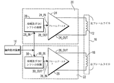
図1を参照すると、CRTデバイス例えばCRTモニタ或いはCRTテレビジョンセットなどに対するフレーム駆動回路10が示され、この駆動回路10は偏向処理装置14とフレームコイル16とを含む。本発明によると、このフレーム駆動回路10は、フレームコイル16の第一のコアの半分12と、第二のコアの半分18と、第一のコイルドライバ20と、第二のコイルドライバ22とを含む。
Referring to FIG. 1, a frame driving circuit 10 for a CRT device such as a CRT monitor or a CRT television set is shown, which includes a
偏向処理装置14は、良く知られているように、偏向処理装置出力信号を作成する。この偏向処理装置出力信号は第一のドライバ20と第二のドライバ22の各々に加えられる。第一のドライバ20と第二のドライバ22の各々は、第一のコイル駆動信号と第二のコイル駆動信号とを、偏向処理装置出力信号の関数としてそれぞれ作成するように互いに独立して選択的に作動する。これら第一のコイル駆動信号と第二のコイル駆動信号は、順番に第一のコイルの半分12と第二のコイルの半分18のそれぞれに加えられる。後に示すように、これら2つのコイル信号は振幅が異なってもよいし、一方は他方に対してDCシフトされてもよい。本発明者は、これら2つのコイルに異なる電流を加えるが、ある高性能なCRTディスプレイシステムにおいて用いられる余分な回転コイルを必要としないで、像の傾きを訂正できることに気付いた。この電流差は、像の台形と、回転と、平行四辺形傾斜との修正を可能にする。それぞれのコイル電流の調節は、ディスプレイの製造時にテストを通じて、或いは直接にユーザによる傾き修正設定の間に実行されてもよい。
The
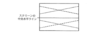
本発明の一つの実施例においては、第一のドライバ20と第二のドライバ22の各々は、偏向処理装置出力信号を、第一のコイル駆動信号と第二のコイル駆動信号の各々を作成するために増幅する。この実施例においては、偏向処理装置出力信号の増幅は、第一のコイル駆動信号と第二のコイル駆動信号が第一のコイルの半分12と第二のコイルの半分18にそれぞれ加えられたとき、図2に最も良く示されるように、それらのコイル駆動信号の合成がCRTモニタの画像の回転を修正するように選択されてもよい。
In one embodiment of the present invention, each of the
この実施例においては、第一のドライバ20と第二のドライバ22の各々による偏向処理装置出力信号の増幅は、CRT画像の回転が一定の周囲の場(constant ambient field)、例えば、地球の磁場によって起こされている場合は、実質的に等しくてもよい。更に、偏向処理装置出力信号の増幅の比も、図4に最も良く示されるように、台形の修正を与えるために選択的に調節されるてもよい。
In this embodiment, the amplification of the deflection processor output signal by each of the
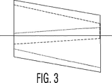
本発明のもう一つの実施例においては、第一のドライバ20と第二のドライバ22の各々は、更に、偏向処理装置出力信号を、第一のコイル駆動信号と第二のコイル駆動信号の各々を作成するために更にDCシフトする。この実施例においては、偏向処理装置出力信号のDCレベルのシフトは、第一のコイル駆動信号と第二のコイル駆動信号とが、それぞれ第一のコイルの半分12と第二のコイルの半分18に加えられたとき、図3に最も良く示されるように、それらのコイル駆動信号の合成がCRTモニタの画像を平行四辺形歪にするように選択されてもよい。
In another embodiment of the present invention, each of the
本発明によると、偏向処理装置出力信号増幅が、独立していようが、ロックステップすなわち比であろうが、DCレベルのシフトと同時であろうが、単独で或いは任意の組合せにて、本発明を実施するために用いられてもよいことが予期される。通常は、CRT画像は幾つかの歪みの形態を示し、これら歪みの訂正は、従来の技術におけるように、歪みの各タイプに対する個別のユーザ設定によって達成される。本発明は、簡素化された装置にてこれら複数のタイプの歪みを同時に訂正することを許す。 In accordance with the present invention, whether the deflection processor output signal amplification is independent, lockstep or ratio, or simultaneous with DC level shifting, either alone or in any combination, the present invention. It is anticipated that it may be used to implement Typically, CRT images exhibit several forms of distortion, and correction of these distortions is achieved by individual user settings for each type of distortion, as in the prior art. The present invention allows these multiple types of distortions to be corrected simultaneously with a simplified apparatus.
したがって、第一のドライバ20と第二のドライバ22の各々は、入力24_IN、26_INと出力24_OUT、26_OUTとを有する増幅器24、26を含む。各々の増幅器24、26の入力24_IN、26_INは、偏向処理装置出力信号を受け取るように適応される。各々の増幅器24、26の出力24_OUT、26_OUTは、第一のコイルの半分12と第二のコイルの半分18のそれぞれに加えるための増幅された信号を作成する。
Accordingly, each of the
第一のドライバ20と第二のドライバ22の各々は、更に、それぞれの入力28_IN、30_INと、それぞれの出力28_OUT、30_OUTとを有するDCレベルシフタ28、30を含んでもよい。各々のDCレベルシフタ28、30の入力28_IN、30_INは偏向処理装置14から偏向処理装置出力信号を受け取るように適応される。各々のDCレベルシフタ28、30の出力28_OUT、30_OUTは、第一のコイルの半分12と第二のコイルの半分18のそれぞれに加えるためのDCレベルシフトされた信号を作成する。各々のドライバ20、22の増幅器24、26とDCレベルシフタ28、30は、直列に接続された別個の要素とすることも、図1に示されるように両方の機能を備えた単一の回路としてもよい。
Each of the
上では本発明の原理に従って構成された新規のフレーム駆動回路が説明された。当業者は、上の説明から、ここに開示された発明の概念から逸脱することなく、上述の実施例の様々な利用、或いはこれらからの離脱を行ってもよい。従って、本発明は、添付のクレームの法的に許される範囲によってのみ記述されるものである。 Above, a novel frame drive circuit constructed in accordance with the principles of the present invention has been described. Those skilled in the art may make various uses of the above-described embodiments or leave them without departing from the inventive concepts disclosed herein from the above description. Accordingly, the invention is to be described only by the legal scope of the appended claims.
Claims (11)
第一のドライバと第二のドライバとを備え、前記偏向処理装置出力信号は前記第一のドライバと第二のドライバの各々に加えられ、前記第一のドライバと第二のドライバの各々は、第一のコイル駆動信号と第二のコイル駆動信号を前記偏向処理装置出力信号の関数としてそれぞれ作成するために互いに独立して選択的に作動し、前記第一のコイル駆動信号と前記第二のコイル駆動信号とはフレームコイルの第一のコイルの半分と第二のコイルの半分のそれぞれに加えられるフレーム駆動回路。A frame driving circuit in a device having a deflection processing device for generating a deflection processing device output signal,
A first driver and a second driver, the deflection processing device output signal is applied to each of the first driver and the second driver, each of the first driver and the second driver, The first coil driving signal and the second coil driving signal are selectively operated independently of each other to create the first coil driving signal and the second coil driving signal as a function of the deflection processing device output signal, The coil drive signal is a frame drive circuit applied to each of the first coil half and the second coil half of the frame coil.
第一のコイル駆動信号と第二のコイル駆動信号を、前記偏向処理装置によって作成される偏向処理装置出力信号の関数として互いに独立して選択的に作成するステップと、
前記第一のコイル駆動信号と前記第二のコイル駆動信号とを前記フレームコイルの第一のコイルの半分と第二のコイルの半分のそれぞれに加えるステップと、
を備える方法。A method for correcting image distortion of a CRT monitor having a deflection processing device and a frame coil, comprising:
Selectively creating a first coil drive signal and a second coil drive signal independently of each other as a function of a deflection processor output signal created by the deflection processor;
Adding the first coil drive signal and the second coil drive signal to each of the first coil half and the second coil half of the frame coil;
A method comprising:
前記偏向処理装置出力信号は前記第一のドライバと前記第二のドライバの各々に加えられ、前記第一のドライバと第二のドライバの各々は、第一のコイル駆動信号と第二のコイル駆動信号を前記偏向処理装置出力信号の関数としてそれぞれ作成するために互いに独立して選択的に作動し、前記第一のコイル駆動信号と前記第二のコイル駆動信号とは前記第一のコイルの半分と前記第二のコイルの半分のそれぞれに加えられることを特徴とするデバイス。A deflection processing device for supplying a deflection processing device output signal, a frame coil having a first coil half and a second coil half, a first driver, and a second driver,
The deflection processing apparatus output signal is applied to each of the first driver and the second driver, and each of the first driver and the second driver includes a first coil driving signal and a second coil driving. Selectively actuated independently of each other to create a signal as a function of the deflection processor output signal, respectively, wherein the first coil drive signal and the second coil drive signal are half of the first coil And a device added to each of the second coil halves.
Applications Claiming Priority (2)
| Application Number | Priority Date | Filing Date | Title |
|---|---|---|---|
| US43134402P | 2002-12-06 | 2002-12-06 | |
| PCT/IB2003/005606 WO2004054236A1 (en) | 2002-12-06 | 2003-12-03 | Drive apparatus for frame deflection and method |
Publications (2)
| Publication Number | Publication Date |
|---|---|
| JP2006509462A JP2006509462A (en) | 2006-03-16 |
| JP4409440B2 true JP4409440B2 (en) | 2010-02-03 |
Family
ID=32507715
Family Applications (1)
| Application Number | Title | Priority Date | Filing Date |
|---|---|---|---|
| JP2004558939A Expired - Fee Related JP4409440B2 (en) | 2002-12-06 | 2003-12-03 | Drive apparatus and method for frame deflection. |
Country Status (8)
| Country | Link |
|---|---|
| US (1) | US8362716B2 (en) |
| EP (1) | EP1570646B8 (en) |
| JP (1) | JP4409440B2 (en) |
| KR (1) | KR20050088098A (en) |
| CN (1) | CN100431334C (en) |
| AU (1) | AU2003283679A1 (en) |
| TW (1) | TW200501739A (en) |
| WO (1) | WO2004054236A1 (en) |
Family Cites Families (15)
| Publication number | Priority date | Publication date | Assignee | Title |
|---|---|---|---|---|
| DE4201700A1 (en) | 1992-01-23 | 1993-07-29 | Thomson Brandt Gmbh | Picture geometry correcting circuit for TV receiver - has prim. winding of transformer connected to output of pulse width modulator with sawtooth and pulse inputs |
| KR970009492B1 (en) * | 1994-05-19 | 1997-06-13 | 삼성전자 주식회사 | Image revising circuit and method in tv |
| US6013989A (en) * | 1996-05-20 | 2000-01-11 | Samsung Electronics Co., Ltd. | Wide-band horizontal linearity correction circuit |
| KR100195907B1 (en) * | 1996-08-27 | 1999-06-15 | 윤종용 | Incline to supplement circuit of screen |
| CN1067198C (en) * | 1996-11-07 | 2001-06-13 | 神达电脑股份有限公司 | Compensation device and method for keystone distortion in north-south direction |
| KR100242839B1 (en) * | 1997-04-14 | 2000-02-01 | 윤종용 | Circuit for controlling screen of monitor |
| KR100242841B1 (en) * | 1997-05-27 | 2000-02-01 | 윤종용 | Circuit for correcting north-south distortion of display apparatus |
| KR100268150B1 (en) * | 1997-05-29 | 2000-10-16 | 윤종용 | Sync-signal regenerating circuit of composite image signal |
| KR100284483B1 (en) * | 1997-12-17 | 2001-03-15 | 이형도 | Misconvergence and geometric distortion correction rules for deflection yokes |
| US6262779B1 (en) * | 1998-02-10 | 2001-07-17 | Hitachi, Ltd | Display apparatus with circuit expanding horizontal retrace interval of horizontal deflection current |
| US6369780B2 (en) * | 1999-09-30 | 2002-04-09 | Thomson Licensing S.A. | Auxiliary deflection winding driver disabling arrangement |
| KR100662573B1 (en) * | 1999-12-23 | 2006-12-28 | 삼성전자주식회사 | A circuit for compensing a horizontal-deflection in a video display system |
| JP2001210255A (en) * | 2000-01-28 | 2001-08-03 | Totoku Electric Co Ltd | Deflection yoke for monochrome tv |
| JP2002094829A (en) * | 2000-09-12 | 2002-03-29 | Mitsubishi Electric Corp | Screen noise removing device and cathode ray tube display unit |
| JP2007107503A (en) | 2005-10-17 | 2007-04-26 | Nissan Diesel Motor Co Ltd | Piston cooling structure |
-
2003
- 2003-12-03 CN CNB2003801049922A patent/CN100431334C/en not_active Expired - Fee Related
- 2003-12-03 AU AU2003283679A patent/AU2003283679A1/en not_active Abandoned
- 2003-12-03 TW TW092134028A patent/TW200501739A/en unknown
- 2003-12-03 WO PCT/IB2003/005606 patent/WO2004054236A1/en active Application Filing
- 2003-12-03 JP JP2004558939A patent/JP4409440B2/en not_active Expired - Fee Related
- 2003-12-03 KR KR1020057010110A patent/KR20050088098A/en not_active Application Discontinuation
- 2003-12-03 US US10/537,673 patent/US8362716B2/en not_active Expired - Fee Related
- 2003-12-03 EP EP03775660A patent/EP1570646B8/en not_active Expired - Lifetime
Also Published As
| Publication number | Publication date |
|---|---|
| US20110007038A1 (en) | 2011-01-13 |
| EP1570646B8 (en) | 2012-12-19 |
| CN1720714A (en) | 2006-01-11 |
| CN100431334C (en) | 2008-11-05 |
| AU2003283679A1 (en) | 2004-06-30 |
| EP1570646A1 (en) | 2005-09-07 |
| US8362716B2 (en) | 2013-01-29 |
| KR20050088098A (en) | 2005-09-01 |
| JP2006509462A (en) | 2006-03-16 |
| EP1570646B1 (en) | 2012-10-24 |
| WO2004054236A1 (en) | 2004-06-24 |
| TW200501739A (en) | 2005-01-01 |
Similar Documents
| Publication | Publication Date | Title |
|---|---|---|
| JP4409440B2 (en) | Drive apparatus and method for frame deflection. | |
| JP2000134507A (en) | Gamma correction circuit | |
| JP2004048758A (en) | Crt focus correction device and method | |
| US5416818A (en) | X-ray TV camera having function to switch a visual field of X-ray image | |
| KR19990016555A (en) | Loupe control of television screen | |
| US6377317B1 (en) | Method and apparatus for correcting color component focusing in a rear-projection television set | |
| US6795065B2 (en) | Display apparatus | |
| US6979944B2 (en) | Display device shared between digital-to-analog converter for outputting convergence signal and dynamic focus signal | |
| KR100265167B1 (en) | Contratst deviation compensation device of display apparatus | |
| KR100265168B1 (en) | Contrast deviation compensation device of display apparatus | |
| US6522091B1 (en) | Circuit and method that allows the amplitudes of vertical correction signal components to be adjusted independently | |
| US7129655B2 (en) | Image distortion correction apparatus capable of correcting misconvergence using an amplifier | |
| KR100263092B1 (en) | Display apparatus of revision device to brightness deflection | |
| US6674253B2 (en) | Scan velocity modulation technique | |
| JP3407677B2 (en) | Speed modulation circuit | |
| EP1565005A1 (en) | Convergence control apparatus for video display | |
| US7158193B2 (en) | Image misconvergence correction apparatus for less switching noise influence | |
| EP1523197A2 (en) | Apparatus and method for adjusting convergence of protection television | |
| JPH11341308A (en) | Image quality adjustment circuit | |
| JPH0779363A (en) | Television video signal processing unit | |
| JPH05161028A (en) | Dynamic focus circuit | |
| JPS60160268A (en) | Color video picture quality adjusting device | |
| JP2004177465A (en) | Crt display | |
| JPH06261219A (en) | Display monitor | |
| JPH08294015A (en) | Cathode ray tube display device |
Legal Events
| Date | Code | Title | Description |
|---|---|---|---|
| A621 | Written request for application examination |
Free format text: JAPANESE INTERMEDIATE CODE: A621 Effective date: 20061201 |
|
| A711 | Notification of change in applicant |
Free format text: JAPANESE INTERMEDIATE CODE: A711 Effective date: 20080619 |
|
| TRDD | Decision of grant or rejection written | ||
| A01 | Written decision to grant a patent or to grant a registration (utility model) |
Free format text: JAPANESE INTERMEDIATE CODE: A01 Effective date: 20091016 |
|
| A01 | Written decision to grant a patent or to grant a registration (utility model) |
Free format text: JAPANESE INTERMEDIATE CODE: A01 |
|
| A61 | First payment of annual fees (during grant procedure) |
Free format text: JAPANESE INTERMEDIATE CODE: A61 Effective date: 20091111 |
|
| R150 | Certificate of patent or registration of utility model |
Free format text: JAPANESE INTERMEDIATE CODE: R150 |
|
| FPAY | Renewal fee payment (event date is renewal date of database) |
Free format text: PAYMENT UNTIL: 20121120 Year of fee payment: 3 |
|
| FPAY | Renewal fee payment (event date is renewal date of database) |
Free format text: PAYMENT UNTIL: 20121120 Year of fee payment: 3 |
|
| S111 | Request for change of ownership or part of ownership |
Free format text: JAPANESE INTERMEDIATE CODE: R313113 |
|
| FPAY | Renewal fee payment (event date is renewal date of database) |
Free format text: PAYMENT UNTIL: 20121120 Year of fee payment: 3 |
|
| R350 | Written notification of registration of transfer |
Free format text: JAPANESE INTERMEDIATE CODE: R350 |
|
| FPAY | Renewal fee payment (event date is renewal date of database) |
Free format text: PAYMENT UNTIL: 20131120 Year of fee payment: 4 |
|
| S111 | Request for change of ownership or part of ownership |
Free format text: JAPANESE INTERMEDIATE CODE: R313113 |
|
| R350 | Written notification of registration of transfer |
Free format text: JAPANESE INTERMEDIATE CODE: R350 |
|
| R250 | Receipt of annual fees |
Free format text: JAPANESE INTERMEDIATE CODE: R250 |
|
| LAPS | Cancellation because of no payment of annual fees |