JP4409244B2 - Optical filter and optical apparatus - Google Patents
Optical filter and optical apparatus Download PDFInfo
- Publication number
- JP4409244B2 JP4409244B2 JP2003354027A JP2003354027A JP4409244B2 JP 4409244 B2 JP4409244 B2 JP 4409244B2 JP 2003354027 A JP2003354027 A JP 2003354027A JP 2003354027 A JP2003354027 A JP 2003354027A JP 4409244 B2 JP4409244 B2 JP 4409244B2
- Authority
- JP
- Japan
- Prior art keywords
- refractive index
- layer
- index layer
- outermost
- laminated
- Prior art date
- Legal status (The legal status is an assumption and is not a legal conclusion. Google has not performed a legal analysis and makes no representation as to the accuracy of the status listed.)
- Expired - Fee Related
Links
- 230000003287 optical effect Effects 0.000 title claims description 70
- 239000000758 substrate Substances 0.000 claims description 64
- 239000010409 thin film Substances 0.000 claims description 28
- 239000012788 optical film Substances 0.000 claims description 19
- 230000008859 change Effects 0.000 claims description 7
- 230000007423 decrease Effects 0.000 claims description 4
- 238000010030 laminating Methods 0.000 claims description 4
- 238000010521 absorption reaction Methods 0.000 description 33
- 230000005540 biological transmission Effects 0.000 description 33
- 239000010408 film Substances 0.000 description 23
- 230000003595 spectral effect Effects 0.000 description 17
- 230000005284 excitation Effects 0.000 description 13
- 239000012528 membrane Substances 0.000 description 13
- 238000002834 transmittance Methods 0.000 description 10
- 230000000694 effects Effects 0.000 description 5
- 239000011521 glass Substances 0.000 description 5
- 238000001514 detection method Methods 0.000 description 4
- 239000006185 dispersion Substances 0.000 description 4
- 230000035945 sensitivity Effects 0.000 description 3
- 230000015572 biosynthetic process Effects 0.000 description 2
- 238000005259 measurement Methods 0.000 description 2
- 238000000034 method Methods 0.000 description 2
- VYPSYNLAJGMNEJ-UHFFFAOYSA-N Silicium dioxide Chemical compound O=[Si]=O VYPSYNLAJGMNEJ-UHFFFAOYSA-N 0.000 description 1
- GWEVSGVZZGPLCZ-UHFFFAOYSA-N Titan oxide Chemical compound O=[Ti]=O GWEVSGVZZGPLCZ-UHFFFAOYSA-N 0.000 description 1
- PNEYBMLMFCGWSK-UHFFFAOYSA-N aluminium oxide Inorganic materials [O-2].[O-2].[O-2].[Al+3].[Al+3] PNEYBMLMFCGWSK-UHFFFAOYSA-N 0.000 description 1
- 239000012472 biological sample Substances 0.000 description 1
- 230000000903 blocking effect Effects 0.000 description 1
- 239000000470 constituent Substances 0.000 description 1
- ORUIBWPALBXDOA-UHFFFAOYSA-L magnesium fluoride Chemical compound [F-].[F-].[Mg+2] ORUIBWPALBXDOA-UHFFFAOYSA-L 0.000 description 1
- 229910001635 magnesium fluoride Inorganic materials 0.000 description 1
- 239000000463 material Substances 0.000 description 1
- 238000012986 modification Methods 0.000 description 1
- 230000004048 modification Effects 0.000 description 1
- BPUBBGLMJRNUCC-UHFFFAOYSA-N oxygen(2-);tantalum(5+) Chemical compound [O-2].[O-2].[O-2].[O-2].[O-2].[Ta+5].[Ta+5] BPUBBGLMJRNUCC-UHFFFAOYSA-N 0.000 description 1
- 230000000737 periodic effect Effects 0.000 description 1
- 230000035699 permeability Effects 0.000 description 1
- 230000008569 process Effects 0.000 description 1
- 230000000630 rising effect Effects 0.000 description 1
- 229910052814 silicon oxide Inorganic materials 0.000 description 1
- 238000004088 simulation Methods 0.000 description 1
- 238000004544 sputter deposition Methods 0.000 description 1
- 229910001936 tantalum oxide Inorganic materials 0.000 description 1
- OGIDPMRJRNCKJF-UHFFFAOYSA-N titanium oxide Inorganic materials [Ti]=O OGIDPMRJRNCKJF-UHFFFAOYSA-N 0.000 description 1
Images


Classifications
-
- G—PHYSICS
- G02—OPTICS
- G02B—OPTICAL ELEMENTS, SYSTEMS OR APPARATUS
- G02B21/00—Microscopes
- G02B21/16—Microscopes adapted for ultraviolet illumination ; Fluorescence microscopes
-
- G—PHYSICS
- G02—OPTICS
- G02B—OPTICAL ELEMENTS, SYSTEMS OR APPARATUS
- G02B5/00—Optical elements other than lenses
- G02B5/20—Filters
- G02B5/28—Interference filters
- G02B5/285—Interference filters comprising deposited thin solid films
-
- G—PHYSICS
- G02—OPTICS
- G02B—OPTICAL ELEMENTS, SYSTEMS OR APPARATUS
- G02B5/00—Optical elements other than lenses
- G02B5/20—Filters
- G02B5/28—Interference filters
- G02B5/289—Rugate filters
Description
本発明は、光学フィルタ及び光学機器に関する。 The present invention relates to an optical filter and an optical apparatus.
生体試料の観察などに用いられる光学機器である蛍光顕微鏡は、染色処理した細胞などの被検体へ励起光を当てた際に被検体が発する蛍光を観察することにより、被検体の構造や性質を解析することができる。
近年のゲノム解析用としては、例えば、502nmの波長を有する励起光で526nmにピークを有する蛍光を観察するというニーズがある。この場合、励起光と蛍光の波長が近いので、蛍光を効率よく検出するために励起光を阻止帯域でカットし蛍光観察波長の光を透過帯域で透過させる光学フィルタが、蛍光測定の感度と精度を決める非常に重要なキーパーツとして用いられている。
A fluorescence microscope, which is an optical instrument used to observe biological samples, observes the fluorescence emitted by the subject when the excitation light is applied to the subject, such as stained cells. Can be analyzed.
For recent genome analysis, for example, there is a need to observe fluorescence having a peak at 526 nm with excitation light having a wavelength of 502 nm. In this case, since the excitation light and the fluorescence wavelength are close to each other, an optical filter that cuts the excitation light in the stop band and transmits the light of the fluorescence observation wavelength in the transmission band in order to efficiently detect the fluorescence is sensitive and accurate in fluorescence measurement. It is used as a very important key part.
この光学フィルタには、透過帯域と阻止帯域の境界で分光特性の急峻な立ち上がりをもち、かつ、透過帯域でほぼ100%の光を透過する性能が要求されている。
このような、所定の波長帯域の光を遮断し、その他の波長の光を透過する光学フィルタはマイナスフィルタと呼ばれ、基板上に高屈折率層と低屈折率層を交互に積層した多層膜で作製される。
This optical filter is required to have a sharp rise in spectral characteristics at the boundary between the transmission band and the stop band and to transmit almost 100% of light in the transmission band.
Such an optical filter that blocks light of a predetermined wavelength band and transmits light of other wavelengths is called a minus filter, and is a multilayer film in which high refractive index layers and low refractive index layers are alternately stacked on a substrate. It is made with.
この光学フィルタは、膜の屈折率を膜厚方向に周期的かつ連続的に変化させ、その屈折率分布をWavelet(波束)と呼ばれる形状にすると、透過帯域における透過率の周期的な変動(リップル)を原理的になくすことができるとともに、上述の層数を増やすほど透過帯域と阻止帯域の境界の立ち上がりを急峻にすることができる(例えば、非特許文献1参照。)。この原理を適用したものを図14(a)に示す。
ただし、実際の成膜時に膜の屈折率を連続的に変化させるのは非常に困難である。そこで、連続的な屈折率分布を階段状に分割して近似して変化させたものが各種提案されている(例えば、特許文献1参照。)。この原理を適用したものを図15(a)に示す。
However, it is very difficult to continuously change the refractive index of the film during actual film formation. Various proposals have been made in which a continuous refractive index distribution is divided into steps and approximated and changed (see, for example, Patent Document 1). An application of this principle is shown in FIG.
しかしながら、上記従来の光学フィルタにおいては、図14(b)及び図15(b)に示すように、阻止帯域近傍の透過帯域において、依然として透過帯域でのリップルが少なからず残存する問題があった。
本発明は上記事情に鑑みて成されたものであり、阻止帯域と透過帯域との境界における分光特性の立ち上がりが急峻で透過帯域でのリップルを抑制して光学特性を安定化した光学フィルタ、及びその光学フィルタを用いることにより、蛍光などでの検出感度を向上した光学機器を提供することを目的とする。
However, in the conventional optical filter, as shown in FIGS. 14 (b) and 15 (b), there is still a problem that ripples in the transmission band still remain in the transmission band near the stop band.
The present invention has been made in view of the above circumstances, an optical filter that stabilizes optical characteristics by suppressing the ripple in the transmission band with a sharp rise in spectral characteristics at the boundary between the stop band and the transmission band, and It is an object of the present invention to provide an optical apparatus having improved detection sensitivity for fluorescence or the like by using the optical filter.
本発明は、上記課題を解決するため、以下の手段を採用する。
本発明に係る光学フィルタは、基板と、該基板上に形成された薄膜とを備え、該薄膜が、前記基板の屈折率よりも低い屈折率を有する光学媒質に接触される最外層部と、屈折率が前記光学媒質の屈折率よりも高い低屈折率層と屈折率が前記低屈折率層の屈折率よりも相対的に高い高屈折率層とが前記基板側に向かって交互に積層されて構成される屈折率変動部とを備え、前記最外層部が、前記光学媒質に接触されるとともに前記光学媒質の屈折率よりも高い屈折率とされる最外低屈折率層と、前記最外低屈折率層に積層され前記最外低屈折率層の屈折率よりも高い屈折率を有する第1の最外高屈折率層と、該第1の最外高屈折率層に積層され前記第1の最外高屈折率層の屈折率よりも高い屈折率を有する第2の最外高屈折率層とを備え、前記屈折率変動部が、前記最外層部に前記低屈折率層が積層され、前記高屈折率層の屈折率が前記第2の最外高屈折率層よりも高い屈折率から前記基板側に向かって漸次高く変化する第1の積層部と、該第1の積層部の基板側に積層され、前記高屈折率層の屈折率が前記基板側に向かって漸次低く変化する第2の積層部と、前記第1の積層部と前記第2の積層部との間に積層され、前記高屈折率層の屈折率が前記第1の積層部を構成する高屈折率層のうち最も高い屈折率と同一である第3の積層部とを備え、前記屈折率変動部が、前記基板側に向かって複数隣接して積層され、複数の前記屈折率変動部の何れか二つを第1の屈折率変動部及び第2の屈折率変動部とするとき、前記第1の屈折率変動部における前記高屈折率層の光学膜厚、前記第1の屈折率変動部における前記低屈折率層の光学膜厚、前記第2の屈折率変動部における前記高屈折率層の光学膜厚、及び前記第2の屈折率変動部における前記低屈折率層の光学膜厚のうち、少なくとも一つが他と異なる膜厚とされていることを特徴とする。
The present invention employs the following means in order to solve the above problems.
An optical filter according to the present invention comprises a substrate and a thin film formed on the substrate, and the thin film is in contact with an optical medium having a refractive index lower than the refractive index of the substrate; A low refractive index layer whose refractive index is higher than the refractive index of the optical medium and a high refractive index layer whose refractive index is relatively higher than the refractive index of the low refractive index layer are alternately laminated toward the substrate side. An outermost low refractive index layer that is in contact with the optical medium and has a refractive index higher than the refractive index of the optical medium; and A first outermost high refractive index layer laminated on the outer low refractive index layer and having a refractive index higher than the refractive index of the outermost low refractive index layer, and laminated on the first outermost high refractive index layer. A second outermost high refractive index layer having a refractive index higher than the refractive index of the first outermost high refractive index layer, The refractive index variable portion is formed by laminating the low refractive index layer on the outermost layer portion, and the refractive index of the high refractive index layer is higher than that of the second outermost high refractive index layer from the refractive index toward the substrate side. A first stacked portion that gradually increases and a second stacked portion that is stacked on the substrate side of the first stacked portion, and the refractive index of the high refractive index layer gradually decreases toward the substrate. And the highest refractive index among the high refractive index layers constituting the first laminated portion, wherein the refractive index of the high refractive index layer is laminated between the first laminated portion and the second laminated portion. A third laminated portion that is the same, and a plurality of the refractive index varying portions are laminated adjacent to each other toward the substrate side, and any two of the plurality of refractive index varying portions are arranged as the first refractive index. When the variable part and the second refractive index variable part are used, the optical film thickness of the high refractive index layer in the first refractive index variable part, the first The optical film thickness of the low refractive index layer in the refractive index fluctuation part, the optical film thickness of the high refractive index layer in the second refractive index fluctuation part, and the low refractive index layer in the second refractive index fluctuation part Of the optical film thicknesses, at least one film thickness is different from the others .
この光学フィルタは、上記の構成を備えているので、光を透過させる際、所定の波長近傍の阻止帯域に相当する光を阻止するとともに、それ以外の波長に相当する透過帯域の光を透過させるフィルタ特性において、透過帯域と阻止帯域との境界を急峻にして透過光量を増加させることができるとともに透過帯域でのリップルを抑制することができる。
また、この光学フィルタは、上記の構成を備えているので、膜厚を変化させることによって、阻止帯域の中心波長の位置を任意の位置に移動させることができるとともに、阻止帯域の幅を任意の大きさに設定することができる。
Since the optical filter has the above-described configuration, when transmitting light, the optical filter blocks light corresponding to a stop band near a predetermined wavelength and transmits light in a transmission band corresponding to other wavelengths. In the filter characteristics, the boundary between the transmission band and the stop band can be made steep to increase the amount of transmitted light, and the ripple in the transmission band can be suppressed.
In addition, since this optical filter has the above-described configuration, by changing the film thickness, the center wavelength position of the stop band can be moved to an arbitrary position, and the width of the stop band can be arbitrarily set. Can be set to size.
また、本発明に係る光学フィルタは、基板と、該基板上に形成された薄膜とを備え、該薄膜が、前記基板の屈折率よりも低い屈折率を有する光学媒質に接触される最外層部と、屈折率が前記光学媒質の屈折率よりも高い低屈折率層と屈折率が前記低屈折率層の屈折率よりも相対的に高い高屈折率層とが前記基板側に向かって交互に積層されて構成される屈折率変動部とを備え、前記最外層部が、前記光学媒質に接触されるとともに前記光学媒質の屈折率よりも高い屈折率とされる最外低屈折率層と、前記最外低屈折率層に積層され前記最外低屈折率層の屈折率よりも高い屈折率を有する第1の最外高屈折率層と、該第1の最外高屈折率層に積層され前記第1の最外高屈折率層の屈折率よりも高い屈折率を有する第2の最外高屈折率層とを備え、前記屈折率変動部が、前記最外層部に前記低屈折率層が積層され、前記高屈折率層の屈折率が前記第2の最外高屈折率層よりも高い屈折率から前記基板側に向かって漸次高く変化し、前記低屈折率層の屈折率が前記最外低屈折率層の屈折率と略同一である第1の積層部と、該第1の積層部の基板側に積層され、前記高屈折率層の屈折率が前記基板側に向かって漸次低く変化し、前記低屈折率層の屈折率が、前記基板側に向かって前記基板の屈折率まで漸次高く変化する第2の積層部と、前記第1の積層部と前記第2の積層部との間に積層され、前記高屈折率層の屈折率が前記第1の積層部を構成する高屈折率層のうち最も高い屈折率と同一であり、前記低屈折率層の屈折率が前記最外低屈折率層の屈折率と略同一である第3の積層部とを備えていることを特徴とする。
この光学フィルタは、上記の構成を備えているので、光を透過させる際、所定の波長近傍の阻止帯域に相当する光を阻止するとともに、それ以外の波長に相当する透過帯域の光を透過させるフィルタ特性において、透過帯域と阻止帯域との境界を急峻にして透過光量を増加させることができるとともに透過帯域でのリップルを抑制することができる。
また、この光学フィルタは、上記の構成を備えているので、基板と薄膜との境界における損失を抑制し、透過帯域における光の透過量をより良好にすることができる。
The optical filter according to the present invention includes a substrate and a thin film formed on the substrate, and the thin film is in contact with an optical medium having a refractive index lower than that of the substrate. And a low refractive index layer having a refractive index higher than the refractive index of the optical medium and a high refractive index layer having a refractive index relatively higher than the refractive index of the low refractive index layer alternately toward the substrate side. An outermost low-refractive-index layer having a refractive index higher than the refractive index of the optical medium, the outermost-layer part being in contact with the optical medium, A first outermost high refractive index layer laminated on the outermost low refractive index layer and having a refractive index higher than that of the outermost low refractive index layer, and laminated on the first outermost high refractive index layer; And a second outermost high refractive index layer having a refractive index higher than that of the first outermost high refractive index layer. The refractive index varying portion is formed by laminating the low refractive index layer on the outermost layer portion, and the refractive index of the high refractive index layer is higher than that of the second outermost high refractive index layer on the substrate side. The first refractive index of the low refractive index layer is substantially the same as the refractive index of the outermost low refractive index layer, and the first laminated portion is laminated on the substrate side. The refractive index of the high refractive index layer gradually decreases toward the substrate side, and the refractive index of the low refractive index layer gradually increases to the refractive index of the substrate toward the substrate side. Stacked between the stacked portion, the first stacked portion, and the second stacked portion, the refractive index of the high refractive index layer is the highest among the high refractive index layers constituting the first stacked portion A third laminated portion having the same refractive index as the refractive index of the low refractive index layer and substantially the same as the refractive index of the outermost low refractive index layer. And wherein the are.
Since the optical filter has the above-described configuration, when transmitting light, the optical filter blocks light corresponding to a stop band near a predetermined wavelength and transmits light in a transmission band corresponding to other wavelengths. In the filter characteristics, the boundary between the transmission band and the stop band can be made steep to increase the amount of transmitted light, and the ripple in the transmission band can be suppressed.
In addition, since this optical filter has the above-described configuration, it is possible to suppress loss at the boundary between the substrate and the thin film and to improve the amount of light transmitted in the transmission band.
また、本発明の光学フィルタは、前記第1の屈折率変動部及び前記第2の屈折率変動部を有する光学フィルタであって、前記第1の積層部及び前記第3の積層部における低屈折率層の屈折率が前記最外低屈折率層の屈折率と略同一とされ、前記第2の積層部における低屈折率層の屈折率が、前記基板側に向かって前記基板の屈折率まで漸次高く変化されていることが好ましい。
この光学フィルタは、上記の構成を備えているので、基板と薄膜との境界における損失を抑制し、透過帯域における光の透過量をより良好にすることができる。
The optical filter of the present invention is an optical filter having the first refractive index variation section and the second refractive index variation section , wherein the low refractive index in the first stacked section and the third stacked section is low. The refractive index of the refractive index layer is substantially the same as the refractive index of the outermost low refractive index layer, and the refractive index of the low refractive index layer in the second stacked portion reaches the refractive index of the substrate toward the substrate side. It is preferable that the temperature is gradually increased.
Since this optical filter has the above-described configuration, it is possible to suppress loss at the boundary between the substrate and the thin film and to improve the amount of light transmitted in the transmission band.
本発明に係る光学機器は、上記本発明に係る光学フィルタのうち何れか一つに記載の光学フィルタを備えていることを特徴とする。
この光学機器は、本発明に係る光学フィルタを備えているので、透過させる波長と透過を阻止する波長とが近い場合でも、透過帯域と阻止帯域との間に急峻な境界を有するとともに、透過帯域の波長の光量を削減することなく効率良く透過させて、分光特性に優れるフィルタ性能を有することができる。また、1つの光学フィルタで阻止帯域の幅を任意に設定することができ、簡単な構成の光学系を備えることができる。
An optical instrument according to the present invention includes the optical filter according to any one of the optical filters according to the present invention.
Since this optical apparatus includes the optical filter according to the present invention, even when the wavelength to transmit and the wavelength to block transmission are close, there is a steep boundary between the transmission band and the stop band, and the transmission band Therefore, it is possible to transmit the light efficiently without reducing the amount of light having the wavelength, and to have a filter performance with excellent spectral characteristics. In addition, the width of the stop band can be arbitrarily set with one optical filter, and an optical system with a simple configuration can be provided .
以上説明した本発明においては以下の効果を奏する。
この光学フィルタによれば、阻止帯域と透過帯域との境界における分光特性の立ち上がりが急峻で透過帯域でのリップルを抑制し光学特性を安定させることができる。
また、本発明の光学機器によれば、本発明に係る光学フィルタを備えているので、観察時に不要な光をカットして所望の波長の光を効率よく選択することができ、従来よりも蛍光等の光の検出感度をより向上することができる。
The present invention described above has the following effects.
According to this optical filter, the rising of the spectral characteristic at the boundary between the stop band and the transmission band is steep and the ripple in the transmission band can be suppressed to stabilize the optical characteristic.
In addition, according to the optical instrument of the present invention, since the optical filter according to the present invention is provided, unnecessary light at the time of observation can be cut and light having a desired wavelength can be selected efficiently, and fluorescence can be selected more than before. It is possible to further improve the light detection sensitivity.
次に、本発明の第1の実施形態について、図1及び図2を参照して説明する。
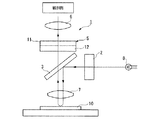
本実施形態に係る図1に示す蛍光顕微鏡(光学機器)1は、励起フィルタ2と、ダイクロイックミラー3と、吸収フィルタ(光学フィルタ)5と、接眼レンズ6と、対物レンズ7とを備える。
Next, a first embodiment of the present invention will be described with reference to FIGS.
A fluorescence microscope (optical apparatus) 1 shown in FIG. 1 according to this embodiment includes an
励起フィルタ2は、光源8から発生した光のうち特定波長のみを選択的に励起光として透過させるように光源8の光路上に配設されている。
ダイクロイックミラー3は、半透過鏡であって、励起フィルタ2を透過した光の光路を載置された、例えば、生体細胞等の標本10上に照射するように変更するとともに、この照射によって標本10から発生した蛍光を観察側に透過するように設定されている。
接眼レンズ6及び対物レンズ7は、上記蛍光を観察できるように調整するものとして配設されている。
The
The
The
吸収フィルタ5は、ガラス製の基板11と、この基板11上に形成された薄膜12とから構成され、上記蛍光のみを選択的に透過させる。
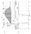
薄膜12は、図2(a)に示すように、基板11の屈折率よりも低い空気(光学媒質)13に接触される最外層部15と、屈折率が空気13の屈折率よりも高く基板11の屈折率以下とされる低屈折率層16と、屈折率が低屈折率層16よりも相対的に高い高屈折率層17とが基板11側に向かって交互に積層されて構成される屈折率変動部18とを備えている。
The
As shown in FIG. 2A, the
最外層部15は、空気13に接触されるとともに空気の屈折率よりも高く基板の屈折率以下の屈折率とされる最外低屈折率層15Aと、最外低屈折率層15Aに積層され最外低屈折率層15Aの屈折率よりも高い屈折率を有する第1の最外高屈折率層15Bと、第1の最外高屈折率層15Bに積層され第1の最外高屈折率層15Bの屈折率よりも高い屈折率を有する第2の最外高屈折率層15Cとを備えている。
The
屈折率変動部18は、最外層部15の基板11側に低屈折率層16が積層され、これに隣接する高屈折率層17の屈折率が第2の最外高屈折率層15Cよりも高い屈折率から基板11側に向かって漸次高く変化する第1の積層部18Aと、第1の積層部18Aの基板11側に積層され、高屈折率層17の屈折率が基板11側に向かって漸次低く変化する第2の積層部18Bと、第1の積層部18Aと第2の積層部18Bとの間に積層され、高屈折率層17の屈折率が第1の積層部18Aを構成する高屈折率層17のうち最も高い屈折率と略同一である第3の積層部18Cとを備えている。
In the refractive
第1の積層部18A及び第3の積層部18Cにおける低屈折率層16の屈折率が最外低屈折率層15Aの屈折率と略同一とされ、第2の積層部18Bにおける低屈折率層16の屈折率が、基板11側に向かって基板11の屈折率まで漸次高く変化されている。
ここで、低屈折率層16は主にフッ化マグネシウムで構成され、高屈折率層17は主に酸化タンタルで構成されている。
本実施形態では、基板11の屈折率を1.52、最外層部15における最外低屈折率層15Aの屈折率を1.4、第1の最外高屈折率層15Bの屈折率を1.5及び第2の最外高屈折率層15Cの屈折率を1.6とし、第1の積層部18Aにおける高屈折率層17を1.7から2.2まで変化させ、第2の積層部18Bにおける高屈折率層17の屈折率を1.52を越えて2.2まで変化させ、第1の積層部18A及び第3の積層部18Cにおける低屈折率層16の屈折率を1.4とし、第2の積層部18Bにおける低屈折率層16の屈折率を1.4から1.52未満の間で変化させている。
The refractive index of the low
Here, the low
In this embodiment, the refractive index of the
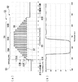
薄膜12は、基板11側から最外層部15の最外低屈折率層15Aまでの積層総数が45層、設計波長が600nmとされ、各層の光学膜厚が設計波長の0.25倍とされている。
各層の屈折率分散はないものとして透過率をシミュレーションした結果を図2(b)に示す。
この吸収フィルタ5は、透過を阻止する中心波長が略610nmで透過率略0%における帯域幅が140nm程度とされる阻止帯域20、及びそれ以外の波長を透過させる透過帯域21A、21Bとを備えている。
In the
FIG. 2B shows the result of simulating the transmittance assuming that there is no refractive index dispersion in each layer.
The
次に、本実施形態に係る蛍光顕微鏡1による観察方法について説明する。
光源8から出射された光を励起フィルタ2を通過させて特定波長の励起光としてダイクロイックミラー3に投射させる。
上記励起光は、ダイクロイックミラー3によって光路を曲げられ、対物レンズ7で集光されて標本10に照射される。このとき、この照射によって標本10から蛍光が発生する。この蛍光は、対物レンズ7を介して平行光となってダイクロイックミラー3に到達し、これを透過して吸収フィルタ5に至る。
Next, an observation method using the
The light emitted from the
The excitation light has its optical path bent by the
吸収フィルタ5に至った蛍光は、最外層部15の最外低屈折率層15Aから入射して、第1の積層部18A、第3の積層部18Cに至り、第2の積層部18Bを透過して基板11側から再び外部へ射出される。
吸収フィルタ5には、蛍光以外の波長を有する励起光等も混入されて入射する。しかし、薄膜12が上述した屈折率変動部16を有する構成とされているので、吸収フィルタ5は、励起光等が属する波長帯域である阻止帯域20における光を外部へ射出させるのを阻止しながら、蛍光が属する波長帯域である透過帯域21A、21Bにおける光を透過させる。
こうして、吸収フィルタ5から射出した蛍光は、接眼レンズ6を透過して集光されて観察側に至る。
The fluorescence that reaches the
Excitation light having a wavelength other than fluorescence is also mixed and incident on the
Thus, the fluorescence emitted from the
この吸収フィルタ5によれば、例えば図2(b)に示すように、阻止帯域20と透過帯域21A、21Bとの境界を急峻にして、透過帯域21A、21Bにおける透過光量を増加するとともにリップルを抑制できる。また、成膜時の膜厚制御が容易な膜構成なので、光学特性の安定性を向上することができる。
さらに、この蛍光顕微鏡1によれば、吸収フィルタ5が図3に示すように理想的なフィルタに近い光学特性を有しているので、従来のフィルタでは透過光量が低下していた波長領域の光量(光量増加分)をも削除することなく透過させることができる。これによって、蛍光測定における検出感度を格段に向上するとともにゲノム解析等における解析精度、検出精度及び観察時間を短縮することができる。
また、低屈折率層16の屈折率が上述のように変化して積層されているので、基板11と薄膜12との境界における損失を抑制し、透過帯域21A、21Bにおける光の透過量をより良好にすることができる。
According to this
Further, according to the
Further, since the refractive index of the low
なお、図4(a)に示すように、薄膜24の屈折率変動部25における第1の積層部25Aについて、積層総数を12層から28層に増やして高屈折率層17の変化率を第1の積層部18Aよりもなだらかに変化させても、図4(b)に示すように、上述と同様の中心波長及び帯域幅を備える阻止帯域20を形成させることができ、図5に示すように最外層部15がない場合と比べて、上述と同様の作用・効果を得ることができる。
また、図6(a)に示すように、屈折率変動部26における第1の積層部26Aの積層総数を12層から4層に減らして高屈折率層17の変化率を第1の積層部18Aよりも急峻に変化させても、図7に示すように最外層部15がない場合と比べて、図6(b)に示すように上述と同様の作用・効果を得ることができる。
As shown in FIG. 4A, for the first
Further, as shown in FIG. 6A, the total number of the first
次に、本発明に係る第2の実施形態について、図8を参照して説明する。なお、以下の説明において、上記実施形態において説明した構成要素には同一符号を付し、その説明は省略する。
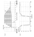
第2の実施形態が第1の実施形態と異なる点は、第1の実施形態では、基板11上に屈折率変動部18が一つだけ積層されているが、第2の実施形態では、吸収フィルタ27の薄膜28の屈折率変動部30が、第1の屈折率変動部31と第2の屈折率変動部32とを備え、これらが順に基板11側に向かって隣接して積層されているとした点である。
Next, a second embodiment according to the present invention will be described with reference to FIG. In the following description, the same reference numerals are given to the components described in the above embodiment, and the description thereof is omitted.
The second embodiment is different from the first embodiment in that, in the first embodiment, only one refractive
すなわち、薄膜28は、図8(a)に示すように、基板11上に第2の屈折率変動部32が積層され、この上に第1の屈折率変動部31が積層され、その上に最外層部15が積層されている。
また、最外層部15の各層の光学膜厚、第1の屈折率変動部31における高屈折率層33の光学膜厚、及び低屈折率層35の光学膜厚が、第2の屈折率変動部32における高屈折率層36の光学膜厚及び低屈折率層37の光学膜厚と異なる膜厚とされている。
本実施形態では、基板11の屈折率が第1の実施形態と同様の1.52とされ、第1の屈折率変動部31における第1の積層部31A、第2の積層部31B、及び第3の積層部31Cの屈折率が、第1の実施形態における屈折率変動部18と同様に変化され、第2の屈折率変動部32における第1の積層部32A及び第2の積層部32Bの低屈折率層37の屈折率が、1.52未満から1.4の間で変化され、第3の積層部32Cの低屈折率層37の屈折率が1.4とされ、高屈折率層36の屈折率が1.52を超えて2.2までの間で変化されている。
That is, as shown in FIG. 8A, the
The optical film thickness of each layer of the
In this embodiment, the refractive index of the
また、薄膜28は、積層総数が基板11上から最外層部15の最外低屈折率層15Aまで89層、設計波長が600nmとされ、第1の屈折率変動部31の各層の光学膜厚を設計波長の0.25倍、第2の屈折率変動部32の各層の光学膜厚を設計波長の0.3倍とされている。
薄膜28各層の屈折率分散はないものとして透過率をシミュレーションした結果を図8(b)に示す。
この吸収フィルタ27は、中心波長が略680nmで透過率略0%における帯域幅が280nm程度とされる阻止帯域38及びそれ以外の波長を透過させる透過帯域40A、40Bを備えている。
The
FIG. 8B shows the result of simulating the transmittance assuming that there is no refractive index dispersion in each layer of the
The
この本実施形態に係る吸収フィルタ27によれば、図9に示すように最外層部15がない場合と比較して、第1の実施形態と同様に蛍光の透過帯域40A、40Bにおけるリップルを小さくして、十分な光量を安定的に得ることができる。また、最外層部15、及び第1の屈折率変動部31と、第2の屈折率変動部32との間で各層の光学膜厚を変化させることによって、阻止帯域38の中心波長の位置を任意の位置に移動させることができるとともに、阻止帯域38の幅を任意の大きさに設定することができる。
According to the
次に、本発明に係る第3の実施形態について、図10を参照して説明する。なお、以下の説明において、第1の実施形態にて説明した構成要素には同一符号を付し、その説明は省略する。
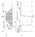
第3の実施形態が上記第1の実施形態と異なる点は、第3の実施形態に係る吸収フィルタ41の薄膜42における最外層部43の各層、及び屈折率変動部45における各層の屈折率を変化させた点である。
Next, a third embodiment according to the present invention will be described with reference to FIG. In the following description, the same reference numerals are given to the components described in the first embodiment, and the description thereof is omitted.
The third embodiment is different from the first embodiment in that the refractive index of each layer of the
すなわち、本実施形態では、図10(a)に示すように、最外層部43における最外低屈折率層43Aの屈折率が1.46とされ、第1の最外高屈折率層43Bの屈折率が1.56、及び第2の最外高屈折率層43Cの屈折率が1.66とされ、第1の積層部45Aにおける高屈折率層46が1.76から2.29まで変化され、第2の積層部45Bにおける高屈折率層46の屈折率が1.52を越えて2.29まで変化され、第1の積層部45A及び第3の積層部45Cにおける低屈折率層47の屈折率が1.46とされ、第2の積層部45Bにおける低屈折率層47の屈折率が1.46から1.52未満の間で変化されている。
薄膜42は、基板11側から最外層部43の最外低屈折率層43Aまでの積層総数が44層、設計波長が600nmとされ、各層の光学膜厚が設計波長の0.25倍とされている。
ここで、低屈折率層47は主に酸化シリコンで構成され、高屈折率層46は主に酸化チタンで構成されている。
That is, in this embodiment, as shown in FIG. 10A, the refractive index of the outermost low
In the
Here, the low
薄膜51の各層の屈折率分散はないものとして透過率をシミュレーションした結果を図10(b)に示す。
この吸収フィルタ41は、中心波長が略610nmで透過率略0%における帯域幅が140nm程度とされる阻止帯域48及びそれ以外の波長を透過させる透過帯域50A、50Bを備えている。
この本実施形態に係る吸収フィルタ41によれば、各層の屈折率が第1の実施形態における屈折率と異なる場合でも、図11に示すように最外層部43がない場合と比較して、第1の実施形態と同様の作用・効果を得ることができ、透過帯域50A、50Bにおけるリップルを低減させることができる。
また、第1の実施形態における各層の構成材料よりもスパッタリングへの適用が容易である等、成膜プロセスの自由度を高めることができる。
FIG. 10B shows the result of simulating the transmittance assuming that there is no refractive index dispersion in each layer of the
The
According to the
In addition, the degree of freedom of the film forming process can be increased, such as being easier to apply to sputtering than the constituent materials of each layer in the first embodiment.
次に、本発明に係る第4の実施形態について、図12を参照して説明する。なお、以下の説明において、上記実施形態において説明した構成要素には同一符号を付し、その説明は省略する。
第4の実施形態が第3の実施形態と異なる点は、図12(a)に示すように、第4の実施形態に係る吸収フィルタ51の薄膜52は、最外層部53が空気13ではなく屈折率1.46のガラス(光学媒質)55と接しているとした点である。
また、ガラス55の屈折率との差を明確にするため、最外低屈折率層53Aと、第1の積層部56A及び第3の積層部56Cにおける低屈折率層57との屈折率が1.67とされ、第2の積層部56Bにおける低屈折率層57の屈折率が1.67を超えて2.29まで変化されている。
Next, a fourth embodiment according to the present invention will be described with reference to FIG. In the following description, the same reference numerals are given to the components described in the above embodiment, and the description thereof is omitted.
The fourth embodiment is different from the third embodiment in that, as shown in FIG. 12A, the
Further, in order to clarify the difference from the refractive index of the glass 55, the refractive index of the outermost low refractive index layer 53A and the low
さらに、第1の最外高屈折率層53Bの屈折率が1.72、第2の最外高屈折率層53Cの屈折率が1.8とされ、第1の積層部56Aにおける高屈折率層58の屈折率が1.8を越えて2.29までの間で変化されている。
また、薄膜52は、基板11側から最外層部53の最外低屈折率層53Aまでの積層総数が44層、設計波長が600nmとされ、各層の光学膜厚が設計波長の0.25倍とされている。
ここで、最外低屈折率層53A及び低屈折率層57は主にアルミナで構成されている。
Further, the refractive index of the first outermost high
The
Here, the outermost low refractive index layer 53A and the low
薄膜52の各層の屈折率分散はないものとして透過率をシミュレーションした結果を図12(b)に示す。
この吸収フィルタ51は、中心波長が略610nmで透過率略0%における帯域幅が90nm程度とされる阻止帯域60及びそれ以外の波長を透過させる透過帯域61A、61Bを備えている。
この本実施形態に係る吸収フィルタ51によれば、最外層部53がガラス55のような空気13以外の光学媒質に接する場合でも、図13に示すように最外層部43がない場合と比較して、第3の実施形態と同様の作用・効果を得ることができる。
FIG. 12B shows the result of simulation of the transmittance assuming that there is no refractive index dispersion in each layer of the
The
According to the
なお、本発明の技術範囲は上記実施の形態に限定されるものではなく、本発明の趣旨を逸脱しない範囲において種々の変更を加えることが可能である。
例えば、上記実施形態における高屈折率層及び低屈折率層の変化率は、直線或いは曲線であるが、変化率はどのような値でも構わない。
The technical scope of the present invention is not limited to the above embodiment, and various modifications can be made without departing from the spirit of the present invention.
For example, the change rate of the high refractive index layer and the low refractive index layer in the above embodiment is a straight line or a curve, but the change rate may be any value.
1 蛍光顕微鏡(光学機器)
5、27、41、51 吸収フィルタ(光学フィルタ)
11 基板
12、24、28、42、52 薄膜
13 空気(光学媒質)
15、43、53 最外層部
15A、43A、53A 最外低屈折率層
15B、43B 第1の最外高屈折率層
15C、43C 第2の最外高屈折率層
16、35、37、47、57 低屈折率層
17、33、36、46、58 高屈折率層
18、25、26、30、45 屈折率変動部
18A、25A、26A、32A、45A、56A 第1の積層部
18B、32B、45B、56B 第2の積層部
18C、32C、45C、56C 第3の積層部
31 第1の屈折率変動部
32 第2の屈折率変動部
55 ガラス(光学媒質)
1 Fluorescence microscope (optical equipment)
5, 27, 41, 51 Absorption filter (optical filter)
11
15, 43, 53
Claims (4)
該薄膜が、前記基板の屈折率よりも低い屈折率を有する光学媒質に接触される最外層部と、
屈折率が前記光学媒質の屈折率よりも高い低屈折率層と屈折率が前記低屈折率層の屈折率よりも相対的に高い高屈折率層とが前記基板側に向かって交互に積層されて構成される屈折率変動部とを備え、
前記最外層部が、前記光学媒質に接触されるとともに前記光学媒質の屈折率よりも高い屈折率とされる最外低屈折率層と、
前記最外低屈折率層に積層され前記最外低屈折率層の屈折率よりも高い屈折率を有する第1の最外高屈折率層と、
該第1の最外高屈折率層に積層され前記第1の最外高屈折率層の屈折率よりも高い屈折率を有する第2の最外高屈折率層とを備え、
前記屈折率変動部が、前記最外層部に前記低屈折率層が積層され、前記高屈折率層の屈折率が前記第2の最外高屈折率層よりも高い屈折率から前記基板側に向かって漸次高く変化する第1の積層部と、
該第1の積層部の基板側に積層され、前記高屈折率層の屈折率が前記基板側に向かって漸次低く変化する第2の積層部と、
前記第1の積層部と前記第2の積層部との間に積層され、前記高屈折率層の屈折率が前記第1の積層部を構成する高屈折率層のうち最も高い屈折率と同一である第3の積層部とを備え、
前記屈折率変動部が、前記基板側に向かって複数隣接して積層され、
複数の前記屈折率変動部の何れか二つを第1の屈折率変動部及び第2の屈折率変動部とするとき、
前記第1の屈折率変動部における前記高屈折率層の光学膜厚、前記第1の屈折率変動部における前記低屈折率層の光学膜厚、前記第2の屈折率変動部における前記高屈折率層の光学膜厚、及び前記第2の屈折率変動部における前記低屈折率層の光学膜厚のうち、少なくとも一つが他と異なる膜厚とされていることを特徴とする光学フィルタ。 A substrate and a thin film formed on the substrate;
An outermost layer portion in which the thin film is in contact with an optical medium having a refractive index lower than that of the substrate;
A low refractive index layer whose refractive index is higher than the refractive index of the optical medium and a high refractive index layer whose refractive index is relatively higher than the refractive index of the low refractive index layer are alternately laminated toward the substrate side. And a refractive index varying portion configured as
An outermost low refractive index layer in which the outermost layer portion is in contact with the optical medium and has a refractive index higher than the refractive index of the optical medium;
A first outermost high refractive index layer laminated on the outermost low refractive index layer and having a refractive index higher than that of the outermost low refractive index layer;
A second outermost high-refractive index layer stacked on the first outermost high-refractive index layer and having a refractive index higher than that of the first outermost high-refractive index layer,
The refractive index varying portion is formed by laminating the low refractive index layer on the outermost layer portion, and the refractive index of the high refractive index layer is higher than that of the second outermost high refractive index layer on the substrate side. A first stacked portion that gradually increases toward
A second laminated portion that is laminated on the substrate side of the first laminated portion, and the refractive index of the high refractive index layer gradually decreases toward the substrate side;
The high refractive index layer is laminated between the first laminated portion and the second laminated portion, and the refractive index of the high refractive index layer is the same as the highest refractive index of the high refractive index layers constituting the first laminated portion. and a third laminated portion is,
A plurality of the refractive index varying portions are laminated adjacent to the substrate side,
When any two of the plurality of refractive index fluctuation portions are a first refractive index fluctuation portion and a second refractive index fluctuation portion,
The optical film thickness of the high refractive index layer in the first refractive index fluctuation portion, the optical film thickness of the low refractive index layer in the first refractive index fluctuation portion, and the high refraction in the second refractive index fluctuation portion. An optical filter characterized in that at least one of the optical film thickness of the refractive index layer and the optical film thickness of the low refractive index layer in the second refractive index fluctuation portion is different from the others .
該薄膜が、前記基板の屈折率よりも低い屈折率を有する光学媒質に接触される最外層部と、
屈折率が前記光学媒質の屈折率よりも高い低屈折率層と屈折率が前記低屈折率層の屈折率よりも相対的に高い高屈折率層とが前記基板側に向かって交互に積層されて構成される屈折率変動部とを備え、
前記最外層部が、前記光学媒質に接触されるとともに前記光学媒質の屈折率よりも高い屈折率とされる最外低屈折率層と、
前記最外低屈折率層に積層され前記最外低屈折率層の屈折率よりも高い屈折率を有する第1の最外高屈折率層と、
該第1の最外高屈折率層に積層され前記第1の最外高屈折率層の屈折率よりも高い屈折率を有する第2の最外高屈折率層とを備え、
前記屈折率変動部が、前記最外層部に前記低屈折率層が積層され、前記高屈折率層の屈折率が前記第2の最外高屈折率層よりも高い屈折率から前記基板側に向かって漸次高く変化し、前記低屈折率層の屈折率が前記最外低屈折率層の屈折率と略同一である第1の積層部と、
該第1の積層部の基板側に積層され、前記高屈折率層の屈折率が前記基板側に向かって漸次低く変化し、前記低屈折率層の屈折率が、前記基板側に向かって前記基板の屈折率まで漸次高く変化する第2の積層部と、
前記第1の積層部と前記第2の積層部との間に積層され、前記高屈折率層の屈折率が前記第1の積層部を構成する高屈折率層のうち最も高い屈折率と同一であり、前記低屈折率層の屈折率が前記最外低屈折率層の屈折率と略同一である第3の積層部とを備えていることを特徴とする光学フィルタ。 A substrate and a thin film formed on the substrate;
An outermost layer portion in which the thin film is in contact with an optical medium having a refractive index lower than that of the substrate;
A low refractive index layer whose refractive index is higher than the refractive index of the optical medium and a high refractive index layer whose refractive index is relatively higher than the refractive index of the low refractive index layer are alternately laminated toward the substrate side. And a refractive index varying portion configured as
An outermost low refractive index layer in which the outermost layer portion is in contact with the optical medium and has a refractive index higher than the refractive index of the optical medium;
A first outermost high refractive index layer laminated on the outermost low refractive index layer and having a refractive index higher than that of the outermost low refractive index layer;
A second outermost high-refractive index layer stacked on the first outermost high-refractive index layer and having a refractive index higher than that of the first outermost high-refractive index layer,
The refractive index varying portion is formed by laminating the low refractive index layer on the outermost layer portion, and the refractive index of the high refractive index layer is higher than that of the second outermost high refractive index layer on the substrate side. A first layered portion that gradually increases toward the bottom, wherein the refractive index of the low refractive index layer is substantially the same as the refractive index of the outermost low refractive index layer;
Laminated on the substrate side of the first laminated portion, the refractive index of the high refractive index layer gradually decreases toward the substrate side, and the refractive index of the low refractive index layer increases toward the substrate side. A second stack that gradually increases to the refractive index of the substrate;
The high refractive index layer is laminated between the first laminated portion and the second laminated portion, and the refractive index of the high refractive index layer is the same as the highest refractive index of the high refractive index layers constituting the first laminated portion. , and the optical science filter you characterized in that the refractive index of the low refractive index layer and a third laminated portion is substantially the same as the refractive index of the outermost low refractive index layer.
前記第2の積層部における低屈折率層の屈折率が、前記基板側に向かって前記基板の屈折率まで漸次高く変化されていることを特徴とする請求項1に記載の光学フィルタ。 The refractive index of the low refractive index layer in the first laminated portion and the third laminated portion is substantially the same as the refractive index of the outermost low refractive index layer,
The refractive index of the second low refractive index layer in the laminated portion of the optical filter according to claim 1, characterized in that the headed toward the substrate is gradually increased change to the refractive index of the substrate.
Priority Applications (26)
| Application Number | Priority Date | Filing Date | Title |
|---|---|---|---|
| JP2003354027A JP4409244B2 (en) | 2003-10-14 | 2003-10-14 | Optical filter and optical apparatus |
| US10/917,479 US7193780B2 (en) | 2003-08-22 | 2004-08-13 | Optical filter and optical instrument |
| DE602004014687T DE602004014687D1 (en) | 2003-08-22 | 2004-08-17 | Optical multilayer filters with periodic variation of high and low optical refractive index and optical instrument |
| EP08005190A EP1962114A3 (en) | 2003-08-22 | 2004-08-17 | Optical multi-layer filter with periodical variation of the high and low refractive index and optical instrument |
| EP04019510A EP1508822B1 (en) | 2003-08-22 | 2004-08-17 | Optical multi-layer filter with periodical variation of the high and low refractive index and optical instrument |
| EP08005191A EP1962115A3 (en) | 2003-08-22 | 2004-08-17 | Optical multi-layer filter with periodical variation of the high and low refractive index and optical instrument |
| EP08005189A EP1962113A3 (en) | 2003-08-22 | 2004-08-17 | Optical multi-layer filter with periodical variation of the high and low refractive index and optical instrument |
| EP08005188A EP1980880A3 (en) | 2003-08-22 | 2004-08-17 | Optical multi-layer filter with periodical variation of the high and low refractive index and optical instrument |
| EP08005184A EP1956399A3 (en) | 2003-08-22 | 2004-08-17 | Optical multi-layer filter with periodic variation of high and low refractive index and optical instrument |
| EP08005186A EP1956400A3 (en) | 2003-08-22 | 2004-08-17 | Optical multi-layer filter with periodical variation of the high and low refractive index and optical instrument |
| EP08005185A EP1980879A3 (en) | 2003-08-22 | 2004-08-17 | Optical multi-layer filter with periodical variation of the high and low refractive index and optical instrument |
| EP08005193A EP1962117A3 (en) | 2003-08-22 | 2004-08-17 | Optical multi-layer filter with periodical variation of the high and low refractive index and optical instrument |
| EP08005192A EP1962116A3 (en) | 2003-08-22 | 2004-08-17 | Optical multi-layer filter with periodical variation of the high and low refractive index and optical instrument |
| EP08005187A EP1962112A3 (en) | 2003-08-22 | 2004-08-17 | Optical multi-layer filter with periodical variation of the high and low refractive index and optical instrument |
| CNB2004100582507A CN1282882C (en) | 2003-08-22 | 2004-08-20 | Optical filter and optical instrument |
| EP04024085A EP1524535A1 (en) | 2003-10-14 | 2004-10-08 | Optical multi-layer filter with periodical variation of the high and low refractive index and optical instrument |
| US10/960,499 US7130125B2 (en) | 2003-10-14 | 2004-10-08 | Optical filter and optical device |
| CNB200410085574XA CN1333272C (en) | 2003-10-14 | 2004-10-12 | Optical filter and optical instrument |
| US11/645,904 US7369314B2 (en) | 2003-08-22 | 2006-12-26 | Optical filter and optical instrument |
| US11/646,931 US7274512B2 (en) | 2003-08-22 | 2006-12-27 | Optical filter and optical instrument |
| US11/646,916 US7289268B2 (en) | 2003-08-22 | 2006-12-27 | Optical filter and optical instrument |
| US11/646,969 US7324283B2 (en) | 2003-08-22 | 2006-12-27 | Optical filter and optical instrument |
| US11/648,461 US7277228B2 (en) | 2003-08-22 | 2006-12-28 | Optical filter and optical instrument |
| US11/647,667 US7312925B2 (en) | 2003-08-22 | 2006-12-28 | Optical filter and optical instrument |
| US11/649,045 US7265905B2 (en) | 2003-08-22 | 2007-01-02 | Optical filter and optical instrument |
| US11/648,930 US7271959B2 (en) | 2003-08-22 | 2007-01-02 | Optical filter and optical instrument |
Applications Claiming Priority (1)
| Application Number | Priority Date | Filing Date | Title |
|---|---|---|---|
| JP2003354027A JP4409244B2 (en) | 2003-10-14 | 2003-10-14 | Optical filter and optical apparatus |
Publications (3)
| Publication Number | Publication Date |
|---|---|
| JP2005121731A JP2005121731A (en) | 2005-05-12 |
| JP2005121731A5 JP2005121731A5 (en) | 2006-11-30 |
| JP4409244B2 true JP4409244B2 (en) | 2010-02-03 |
Family
ID=34373551
Family Applications (1)
| Application Number | Title | Priority Date | Filing Date |
|---|---|---|---|
| JP2003354027A Expired - Fee Related JP4409244B2 (en) | 2003-08-22 | 2003-10-14 | Optical filter and optical apparatus |
Country Status (4)
| Country | Link |
|---|---|
| US (1) | US7130125B2 (en) |
| EP (1) | EP1524535A1 (en) |
| JP (1) | JP4409244B2 (en) |
| CN (1) | CN1333272C (en) |
Families Citing this family (2)
| Publication number | Priority date | Publication date | Assignee | Title |
|---|---|---|---|---|
| CN101893729B (en) * | 2010-07-22 | 2011-12-07 | 中国航空工业集团公司洛阳电光设备研究所 | Intermediate infrared bandpass filter and preparation method thereof |
| CN109765645A (en) * | 2019-03-15 | 2019-05-17 | 深圳大学 | A kind of porous pectinate texture optical thin film and preparation method thereof |
Family Cites Families (8)
| Publication number | Priority date | Publication date | Assignee | Title |
|---|---|---|---|---|
| US4309075A (en) | 1979-10-05 | 1982-01-05 | Optical Coating Laboratory, Inc. | Multilayer mirror with maximum reflectance |
| US4756602A (en) | 1987-06-05 | 1988-07-12 | Rockwell International Corporation | Narrowband optical filter with partitioned cavity |
| JPH10174652A (en) | 1996-12-18 | 1998-06-30 | Kanazawa Kogyo Kk | Coffee maker |
| US5907427A (en) * | 1997-10-24 | 1999-05-25 | Time Domain Corporation | Photonic band gap device and method using a periodicity defect region to increase photonic signal delay |
| JP3290629B2 (en) * | 1998-06-22 | 2002-06-10 | アルプス電気株式会社 | Optical multilayer filter |
| US6611378B1 (en) | 2001-12-20 | 2003-08-26 | Semrock, Inc. | Thin-film interference filter with quarter-wavelength unit sub-layers arranged in a generalized pattern |
| US7193780B2 (en) * | 2003-08-22 | 2007-03-20 | Olympus Corporation | Optical filter and optical instrument |
| JP4575052B2 (en) * | 2004-07-07 | 2010-11-04 | オリンパス株式会社 | Multilayer negative filter and fluorescence microscope |
-
2003
- 2003-10-14 JP JP2003354027A patent/JP4409244B2/en not_active Expired - Fee Related
-
2004
- 2004-10-08 EP EP04024085A patent/EP1524535A1/en not_active Withdrawn
- 2004-10-08 US US10/960,499 patent/US7130125B2/en active Active
- 2004-10-12 CN CNB200410085574XA patent/CN1333272C/en not_active Expired - Fee Related
Also Published As
| Publication number | Publication date |
|---|---|
| JP2005121731A (en) | 2005-05-12 |
| CN1607405A (en) | 2005-04-20 |
| CN1333272C (en) | 2007-08-22 |
| EP1524535A1 (en) | 2005-04-20 |
| US20050111103A1 (en) | 2005-05-26 |
| US7130125B2 (en) | 2006-10-31 |
Similar Documents
| Publication | Publication Date | Title |
|---|---|---|
| US7324283B2 (en) | Optical filter and optical instrument | |
| JP4575052B2 (en) | Multilayer negative filter and fluorescence microscope | |
| JP4331546B2 (en) | Optical filter and optical apparatus | |
| JP4409244B2 (en) | Optical filter and optical apparatus | |
| JP4468667B2 (en) | Optical filter and optical apparatus | |
| JP2017009704A (en) | Optical element using multi-layer film, optical system and optical device | |
| JP4469016B2 (en) | Optical filter and optical apparatus | |
| US20080030858A1 (en) | Optical filter and optical apparatus | |
| JP4331547B2 (en) | Optical filter and optical apparatus | |
| JP4343620B2 (en) | Optical filter and optical apparatus | |
| JP4608585B2 (en) | Optical filter and optical apparatus | |
| JP4531108B2 (en) | Optical filter and optical apparatus | |
| CN114919250B (en) | Dark field imaging glass slide based on multi-angle tunable filter film | |
| JPH0718961B2 (en) | Bandpass filter | |
| JP2008299244A (en) | Long wavelength band cut multilayer film, infrared cut multilayer film, optical element and optical filter having them, and medical endoscope using them |
Legal Events
| Date | Code | Title | Description |
|---|---|---|---|
| A521 | Request for written amendment filed |
Free format text: JAPANESE INTERMEDIATE CODE: A523 Effective date: 20061011 |
|
| A621 | Written request for application examination |
Free format text: JAPANESE INTERMEDIATE CODE: A621 Effective date: 20061011 |
|
| A521 | Request for written amendment filed |
Free format text: JAPANESE INTERMEDIATE CODE: A821 Effective date: 20061012 |
|
| A131 | Notification of reasons for refusal |
Free format text: JAPANESE INTERMEDIATE CODE: A131 Effective date: 20090728 |
|
| A521 | Request for written amendment filed |
Free format text: JAPANESE INTERMEDIATE CODE: A523 Effective date: 20090918 |
|
| A521 | Request for written amendment filed |
Free format text: JAPANESE INTERMEDIATE CODE: A821 Effective date: 20090924 |
|
| TRDD | Decision of grant or rejection written | ||
| A01 | Written decision to grant a patent or to grant a registration (utility model) |
Free format text: JAPANESE INTERMEDIATE CODE: A01 Effective date: 20091020 |
|
| A01 | Written decision to grant a patent or to grant a registration (utility model) |
Free format text: JAPANESE INTERMEDIATE CODE: A01 |
|
| A61 | First payment of annual fees (during grant procedure) |
Free format text: JAPANESE INTERMEDIATE CODE: A61 Effective date: 20091111 |
|
| R151 | Written notification of patent or utility model registration |
Ref document number: 4409244 Country of ref document: JP Free format text: JAPANESE INTERMEDIATE CODE: R151 |
|
| FPAY | Renewal fee payment (event date is renewal date of database) |
Free format text: PAYMENT UNTIL: 20121120 Year of fee payment: 3 |
|
| FPAY | Renewal fee payment (event date is renewal date of database) |
Free format text: PAYMENT UNTIL: 20131120 Year of fee payment: 4 |
|
| S531 | Written request for registration of change of domicile |
Free format text: JAPANESE INTERMEDIATE CODE: R313531 |
|
| R350 | Written notification of registration of transfer |
Free format text: JAPANESE INTERMEDIATE CODE: R350 |
|
| R250 | Receipt of annual fees |
Free format text: JAPANESE INTERMEDIATE CODE: R250 |
|
| LAPS | Cancellation because of no payment of annual fees |