JP4401814B2 - Standard member for length measurement and electron beam length measuring device - Google Patents
Standard member for length measurement and electron beam length measuring device Download PDFInfo
- Publication number
- JP4401814B2 JP4401814B2 JP2004049218A JP2004049218A JP4401814B2 JP 4401814 B2 JP4401814 B2 JP 4401814B2 JP 2004049218 A JP2004049218 A JP 2004049218A JP 2004049218 A JP2004049218 A JP 2004049218A JP 4401814 B2 JP4401814 B2 JP 4401814B2
- Authority
- JP
- Japan
- Prior art keywords
- diffraction grating
- pattern
- grating unit
- electron beam
- pitch
- Prior art date
- Legal status (The legal status is an assumption and is not a legal conclusion. Google has not performed a legal analysis and makes no representation as to the accuracy of the status listed.)
- Expired - Fee Related
Links
Images


Classifications
-
- H—ELECTRICITY
- H01—ELECTRIC ELEMENTS
- H01J—ELECTRIC DISCHARGE TUBES OR DISCHARGE LAMPS
- H01J37/00—Discharge tubes with provision for introducing objects or material to be exposed to the discharge, e.g. for the purpose of examination or processing thereof
- H01J37/26—Electron or ion microscopes; Electron or ion diffraction tubes
- H01J37/28—Electron or ion microscopes; Electron or ion diffraction tubes with scanning beams
-
- G—PHYSICS
- G01—MEASURING; TESTING
- G01B—MEASURING LENGTH, THICKNESS OR SIMILAR LINEAR DIMENSIONS; MEASURING ANGLES; MEASURING AREAS; MEASURING IRREGULARITIES OF SURFACES OR CONTOURS
- G01B15/00—Measuring arrangements characterised by the use of electromagnetic waves or particle radiation, e.g. by the use of microwaves, X-rays, gamma rays or electrons
-
- G—PHYSICS
- G01—MEASURING; TESTING
- G01B—MEASURING LENGTH, THICKNESS OR SIMILAR LINEAR DIMENSIONS; MEASURING ANGLES; MEASURING AREAS; MEASURING IRREGULARITIES OF SURFACES OR CONTOURS
- G01B21/00—Measuring arrangements or details thereof, where the measuring technique is not covered by the other groups of this subclass, unspecified or not relevant
- G01B21/02—Measuring arrangements or details thereof, where the measuring technique is not covered by the other groups of this subclass, unspecified or not relevant for measuring length, width, or thickness
- G01B21/04—Measuring arrangements or details thereof, where the measuring technique is not covered by the other groups of this subclass, unspecified or not relevant for measuring length, width, or thickness by measuring coordinates of points
- G01B21/042—Calibration or calibration artifacts
-
- H—ELECTRICITY
- H01—ELECTRIC ELEMENTS
- H01J—ELECTRIC DISCHARGE TUBES OR DISCHARGE LAMPS
- H01J2237/00—Discharge tubes exposing object to beam, e.g. for analysis treatment, etching, imaging
- H01J2237/26—Electron or ion microscopes
- H01J2237/28—Scanning microscopes
- H01J2237/2813—Scanning microscopes characterised by the application
- H01J2237/2814—Measurement of surface topography
-
- H—ELECTRICITY
- H01—ELECTRIC ELEMENTS
- H01J—ELECTRIC DISCHARGE TUBES OR DISCHARGE LAMPS
- H01J2237/00—Discharge tubes exposing object to beam, e.g. for analysis treatment, etching, imaging
- H01J2237/26—Electron or ion microscopes
- H01J2237/282—Determination of microscope properties
- H01J2237/2826—Calibration
Description
本発明は、電子ビーム測長に用いられる測長用標準部材を含む電子ビーム測長技術に関する。 The present invention relates to an electron beam length measurement technique including a length measurement standard member used for electron beam length measurement.
従来の測電子ビーム測長に用いられる測長用標準部材は、半導体基板上にレーザ干渉露光と異方性湿式エッチングにより作製した回折格子が用いられてきた。その校正方法は、波長の絶対精度が保証されたレーザ光を用いた回折格子の回折角測定により行われている(例えば、特許文献1参照)。 As a standard member for length measurement used in conventional electron beam measurement, a diffraction grating produced on a semiconductor substrate by laser interference exposure and anisotropic wet etching has been used. The calibration method is performed by measuring the diffraction angle of a diffraction grating using a laser beam whose absolute wavelength accuracy is guaranteed (see, for example, Patent Document 1).
上記従来の標準部材で可能な最小寸法は、レーザ干渉露光法の解像限界によっており、用いるレーザ光の波長の2分の1がピッチ寸法の限界である。現在レーザ干渉露光装置で用いられている波長351.1nmのアルゴンイオンレーザではピッチ寸法で約200nmが限界である。また、レーザ光源をより短波長に替えた露光装置も技術課題が多く、開発が困難である。同様に、校正に用いるレーザ光を用いた回折格子の回折角測定でも測定限界があり、最小ピッチ寸法が約200nm以下では計測が困難である。 The minimum dimension possible with the above-mentioned conventional standard member depends on the resolution limit of the laser interference exposure method, and half the wavelength of the laser beam used is the limit of the pitch dimension. The argon ion laser having a wavelength of 351.1 nm currently used in the laser interference exposure apparatus has a limit of about 200 nm in pitch dimension. Also, an exposure apparatus in which the laser light source is changed to a shorter wavelength has many technical problems and is difficult to develop. Similarly, there is a measurement limit in the diffraction angle measurement of a diffraction grating using laser light used for calibration, and measurement is difficult when the minimum pitch dimension is about 200 nm or less.
一方、半導体デバイスの微細化が加速されているために最小加工寸法が100nmを切ってきた。この超微細加工の寸法管理には電子ビーム測長装置が用いられているが、かかる装置の絶対精度管理のためには寸法標準部材が不可欠である。しかしながら、従来の寸法標準部材では最新の半導体デバイスの最小加工寸法には対応ができなくなる。 On the other hand, since the miniaturization of semiconductor devices has been accelerated, the minimum processing dimension has cut below 100 nm. An electron beam length measuring device is used for dimension management of this ultrafine processing, but a dimension standard member is indispensable for managing the absolute accuracy of such an apparatus. However, the conventional dimensional standard member cannot cope with the minimum processing dimension of the latest semiconductor device.
また、レーザ干渉露光法を用いた回折格子パターニングでは、単純なライン&スペースパターンしか原理的に作製できない。このために試料全面に同じパターンができてしまうので、位置決めマークを形成できないため寸法を値付けする装置および測長装置での校正時にどの位置の回折格子パターンを使ったのか厳密には特定できない。電子ビーム測長装置の場合には、ビーム照射に伴うコンタミネ−ション付着のため試料の寸法変動を引き起こすために、特定のパターンを使い続けると校正精度の劣化を引き起こす。 Further, in diffraction grating patterning using laser interference exposure, only simple line and space patterns can be produced in principle. For this reason, the same pattern is formed on the entire surface of the sample. Therefore, since a positioning mark cannot be formed, it is not possible to precisely specify the position of the diffraction grating pattern used in calibration with a device for pricing dimensions and a length measuring device. In the case of the electron beam length measuring device, the dimensional variation of the sample is caused due to the contamination adhering to the irradiation of the beam. Therefore, if a specific pattern is continuously used, the calibration accuracy is deteriorated.
本発明は、上記の点に鑑みてなされたものであり、より微細な基準寸法を有する測長用標準部材を提供し、かつ、それを含む高精度電子ビーム測長技術を提供することを目的とする。 The present invention has been made in view of the above points, and provides a standard member for length measurement having a finer reference dimension and an object of providing a high-precision electron beam length measurement technique including the same. And
上記目的を達成するために、本発明では、従来の回折格子パターンとは別にさらに微細なパターン領域を複数同一半導体部材上に形成することを基本構成とする。すなわち、従来の回折格子パターンであるピッチ寸法約200nm以上の回折格子パターンを、レーザ光を用いた回折格子の回折角測定によりそのピッチ寸法を求め、絶対寸法として用いる。この回折格子パターンとは別に、最小ピッチ寸法が100nm以下の格子パターンを同一半導体部材上に形成する。このパターンの値付けは、従来の波長が絶対的に保証されたレーザ光を用いた回折格子の回折角測定では不可能なので、電子ビーム測長装置もしくは探針プローブ顕微鏡を用い、または波長が絶対的に保証されてはいない極紫外光の短波長レーザを用い、絶対寸法値として上記で求めた従来の回折格子パターンのピッチ寸法を基準として用いる。 In order to achieve the above object, the basic configuration of the present invention is to form a plurality of finer pattern regions on the same semiconductor member separately from the conventional diffraction grating pattern. That is, a diffraction grating pattern having a pitch dimension of about 200 nm or more, which is a conventional diffraction grating pattern, is obtained by measuring the diffraction angle of the diffraction grating using laser light, and used as an absolute dimension. Apart from this diffraction grating pattern, a grating pattern having a minimum pitch dimension of 100 nm or less is formed on the same semiconductor member. Since pattern pricing is not possible with the conventional diffraction angle measurement of diffraction gratings using laser light whose wavelength is absolutely guaranteed, an electron beam length measuring device or a probe probe microscope is used, or the wavelength is absolute. A short wavelength laser of extreme ultraviolet light, which is not guaranteed, is used, and the pitch dimension of the conventional diffraction grating pattern obtained above is used as an absolute dimension value as a reference.
これにより、電子ビームや探針プローブの同一走査範囲以上の長さのパターンを配置させることで位置決めの容易な校正が可能となる。また、このパターンの近傍に他のパターンと区別が容易な形状をしたマークパターンを配置することで電子ビームや探針プローブで測定した位置情報を記録しておくことが可能である。このように、従来のレーザ光を用いた回折格子の回折角測定が可能なパターンと最新の半導体デバイスの最小加工寸法に対応した微細パターンを同一部材内に配置させることで微細性と高精度を両立した寸法標準部材および校正が可能となる。 Accordingly, it is possible to easily calibrate the positioning by arranging a pattern having a length longer than the same scanning range of the electron beam or the probe probe. In addition, it is possible to record position information measured by an electron beam or a probe probe by arranging a mark pattern having a shape that can be easily distinguished from other patterns in the vicinity of this pattern. In this way, the fine pattern and the high accuracy can be achieved by arranging the pattern that can measure the diffraction angle of the diffraction grating using the conventional laser beam and the fine pattern corresponding to the minimum processing dimension of the latest semiconductor device in the same member. A compatible dimensional standard member and calibration are possible.
また、同一部材内に縦方向のパターンと横方向のパターンを配置させることで従来にない縦・横両方の寸法校正が同じ精度で実現できる。これらのパターン単位間の距離を20μm以内にすることで電子ビーム測長装置の光学条件を同じ状態で校正できるので高精度化が実現できる。 In addition, by arranging a vertical pattern and a horizontal pattern in the same member, unprecedented vertical and horizontal dimensional calibration can be realized with the same accuracy. By setting the distance between these pattern units within 20 μm, the optical conditions of the electron beam length measuring device can be calibrated in the same state, so that high accuracy can be realized.
次に、この寸法標準部材の作製について述べる。従来の回折格子パターンと最新の半導体デバイスの最小加工寸法に対応した微細パターンを同一部材内に配置させるには、従来の寸法標準部材で用いたレーザ干渉露光法では解像性およびパターン創生の自由度の点で不可能である。そこで、本発明では、解像性に優れパターン形状の制約のない電子ビーム描画法を用いる。特に、試料面内の均一性を向上させた高精度な寸法標準部材作製のためには、所望のパターンをステンシルマスクに作りこんで電子ビームで縮小投影露光を行う電子ビーム一括図形照射法が有効である。すなわち、複数種の縦横方向の格子状の描画パターンは全てステンシルマスクに作りこんであるので、これをビーム偏向により選択し繰り返し露光することで各ショット毎に寸法変動することはなく再現性の良いパターニングが可能である。このパターニング方法とドライエッチングを組み合わせることにより、微細で電子ビーム測長装置や探針プローブ顕微鏡に適した寸法標準部材の作製が可能になる。また、ステンシルマスクの中に矩形開口を作りこんでおけば、可変成形描画法によりパターン種類数に制限のない描画ができる。 Next, production of this dimensional standard member will be described. In order to arrange the conventional diffraction grating pattern and the fine pattern corresponding to the minimum processing size of the latest semiconductor device in the same member, the laser interference exposure method used in the conventional dimensional standard member requires resolution and pattern creation. It is impossible in terms of degrees of freedom. Therefore, in the present invention, an electron beam drawing method having excellent resolution and no pattern shape restriction is used. In particular, for the production of highly accurate dimensional standard members with improved uniformity in the sample surface, the electron beam batch figure irradiation method, in which a desired pattern is formed on a stencil mask and reduced projection exposure is performed with an electron beam, is effective. It is. That is, a plurality of types of vertical and horizontal grid-like drawing patterns are all built in the stencil mask, so that by selecting and repeating exposure by beam deflection, there is no variation in dimensions for each shot and good reproducibility. Patterning is possible. By combining this patterning method and dry etching, it becomes possible to produce a fine dimensional standard member suitable for an electron beam length measuring device or a probe probe microscope. In addition, if a rectangular opening is formed in the stencil mask, drawing with no limitation on the number of pattern types can be performed by the variable shaping drawing method.
この標準部材で電子ビーム測長装置を校正する際、微細な寸法を測長する場合には、電子ビーム測長装置もしくは探針プローブ顕微鏡を用い、または極紫外光の短波長レーザを用い、値付けした微細な格子パターンで寸法校正を行う。この校正後に波長が絶対的に保証されたレーザ光を用いて、値付けされた回折格子のピッチ寸法を測長することで、上記校正が正しく行われたかを確認できる。上記測定値と回折角で求めたピッチ寸法が基準値を超える場合には、電子ビーム測長装置で警報を発する構成とし、別の微細パターンを用いる。すなわち、マークパターンを基準に、前に測った微細格子以外の場所の微細パターンを用いて再度電子ビーム測長装置を校正することにより、その高い校正精度が維持できる。 When calibrating the electron beam length measuring device with this standard member, when measuring fine dimensions, use an electron beam length measuring device or a probe probe microscope, or use a short wavelength laser of extreme ultraviolet light. Dimension calibration is performed using the fine lattice pattern. It is possible to confirm whether or not the calibration has been performed correctly by measuring the pitch dimension of the diffracted grating that has been priced using laser light whose wavelength is absolutely guaranteed after the calibration. When the pitch dimension obtained by the measured value and the diffraction angle exceeds the reference value, the electron beam length measuring device is configured to issue an alarm, and another fine pattern is used. In other words, the high calibration accuracy can be maintained by calibrating the electron beam length measuring apparatus again using the fine pattern at a place other than the previously measured fine grating on the basis of the mark pattern.
以下、本発明の代表的構成例について述べる。 Hereinafter, typical configuration examples of the present invention will be described.
(1)本発明の測長用標準部材は、基板上に、光学的手段により予めピッチ寸法が求められている回折格子の配列よりなる第1の回折格子単位パターンと、前記第1の回折格子単位パターンよりもピッチ寸法の小さい回折格子の配列よりなる第2の回折格子単位パターンとを含むことを特徴とする。 (1) The length measuring standard member of the present invention includes a first diffraction grating unit pattern composed of an array of diffraction gratings whose pitch dimension is previously obtained by optical means on a substrate, and the first diffraction grating. And a second diffraction grating unit pattern composed of an array of diffraction gratings having a pitch dimension smaller than that of the unit pattern.
(2)前記(1)に記載の測長用標準部材において、前記第2の回折格子単位パターンの最小ピッチ寸法が、100nm以下であることを特徴とする。 (2) In the standard member for length measurement according to (1), the minimum pitch dimension of the second diffraction grating unit pattern is 100 nm or less.
(3)前記(1)に記載の測長用標準部材において、前記基板上に、前記第1の回折格子単位パターンを複数配置した第1のパターン領域と、前記第2の回折格子単位パターンを複数配置した第2のパターン領域を備えたことを特徴とする。 (3) In the standard member for length measurement according to (1), a first pattern region in which a plurality of the first diffraction grating unit patterns are arranged on the substrate, and the second diffraction grating unit pattern are provided. A plurality of second pattern regions are provided.
(4)前記(1)に記載の測長用標準部材において、前記基板上に、測長に使用するプローブ手段の位置決め用マークパターンを備えたことを特徴とする。 (4) The standard member for length measurement according to (1), wherein a positioning mark pattern for probe means used for length measurement is provided on the substrate.
(5)前記(3)に記載の測長用標準部材において、前記第2のパターン領域に、複数の前記第2の回折格子単位パターンの各々の位置情報を含む複数のマークパターンを含むことを特徴とする。 (5) The standard member for length measurement according to (3), wherein the second pattern region includes a plurality of mark patterns including position information of the plurality of second diffraction grating unit patterns. Features.
(6)前記(1)に記載の測長用標準部材において、前記基板上に、前記第1の回折格子単位パターンを構成する前記回折格子とは異なる方向(例えば、縦・横方向)に配列された回折格子よりなる第3の回折格子単位パターンと、前記第2の回折格子単位パターンを構成する前記回折格子とは異なる方向(例えば、縦・横方向)に配列された回折格子よりなる第4の回折格子単位パターンとを有し、前記第4の回折格子単位パターンのピッチ寸法は、前記第3の回折格子単位パターンのピッチ寸法よりも小さいことを特徴とする。 (6) In the standard member for length measurement according to (1), arranged on the substrate in a direction different from the diffraction grating constituting the first diffraction grating unit pattern (for example, vertical and horizontal directions) A third diffraction grating unit pattern composed of the formed diffraction gratings and a first diffraction grating composed of diffraction gratings arranged in different directions (for example, vertical and horizontal directions) from the diffraction grating constituting the second diffraction grating unit pattern. 4, and the pitch dimension of the fourth diffraction grating unit pattern is smaller than the pitch dimension of the third diffraction grating unit pattern.
(7)前記(6)に記載の測長用標準部材において、前記基板上に、前記第1の回折格子単位パターンを複数配置した第1のパターン領域と、前記第2の回折格子単位パターンを複数配置した第2のパターン領域と、前記第3の回折格子単位パターンを複数配置した第3のパターン領域と、前記第4の回折格子単位パターンを複数配置した第4のパターン領域とを備えたことを特徴とする。 (7) In the length measuring standard member according to (6), a first pattern region in which a plurality of the first diffraction grating unit patterns are arranged on the substrate, and the second diffraction grating unit pattern are arranged. A plurality of second pattern areas, a third pattern area where a plurality of the third diffraction grating unit patterns are arranged, and a fourth pattern area where a plurality of the fourth diffraction grating unit patterns are arranged. It is characterized by that.
(8)前記(6)に記載の測長用標準部材において、前記第1の回折格子単位パターンと前記第3の回折格子単位パターンとが互いに格子状に配置され、かつ、前記第2の回折格子単位パターンと前記第4の回折格子単位パターンとが互いに格子状に配置されていることを特徴とする。 (8) In the standard member for length measurement according to (6), the first diffraction grating unit pattern and the third diffraction grating unit pattern are arranged in a lattice pattern, and the second diffraction grating The grating unit pattern and the fourth diffraction grating unit pattern are arranged in a grid pattern.
(9)前記(1)又は(6)に記載の測長用標準部材において、前記各回折格子単位パターン間の距離が、20μm以内であることを特徴とする。 (9) In the standard member for length measurement according to (1) or (6), a distance between the diffraction grating unit patterns is within 20 μm.
(10)本発明の電子ビーム測長装置の校正方法は、電子ビームを試料の所定領域に走査して測長を行なう電子ビーム測長装置を測長用標準部材を用いて校正する方法であって、前記測長用標準部材には、基板上に、光学的手段により予めピッチ寸法が求められている回折格子の配列よりなる第1の回折格子単位パターンと、前記第1の回折格子単位パターンよりもピッチ寸法の小さい回折格子の配列よりなる第2の回折格子単位パターンとを備え、第1の回折格子単位パターンを測長し、その測長結果と前記ピッチ寸法の差を計算して基準値と比較し、前記差が基準値より大きい場合には、前記第2の回折格子単位パターンを測長して前記測長値を校正するようにしたことを特徴とする。 (10) The method for calibrating an electron beam length measuring apparatus according to the present invention is a method for calibrating an electron beam length measuring apparatus that performs length measurement by scanning an electron beam over a predetermined region of a sample using a length measuring standard member. The length measuring standard member includes, on the substrate, a first diffraction grating unit pattern made of an array of diffraction gratings whose pitch dimension is previously determined by optical means, and the first diffraction grating unit pattern. A second diffraction grating unit pattern composed of an array of diffraction gratings having a smaller pitch dimension than the first diffraction grating unit pattern, measuring the first diffraction grating unit pattern, and calculating a difference between the length measurement result and the pitch dimension. When the difference is larger than a reference value, the second diffraction grating unit pattern is measured to calibrate the length measurement value.
(11)本発明の電子ビーム測長装置は、試料を保持する試料ステージと、前記試料ステージ上の試料に対して電子ビームを走査する照射光学系と、前記電子ビーム走査により発生する二次電子線を検出する二次電子検出器と、前記検出器から得られる信号波形を解析することにより前記試料を測長する演算処理手段と、測長結果が表示される表示手段と、前記測長結果を校正するための基準寸法値が格納された記憶手段と、前記試料ステージ上に保持された測長用標準部材とを有し、前記測長用標準部材には、基板上に、光学的手段により予めピッチ寸法が求められている回折格子の配列よりなる第1の回折格子単位パターンと、前記第1の回折格子単位パターンよりもピッチ寸法の小さい複数の回折格子の配列よりなる第2の回折格子単位パターンとを備え、前記演算処理手段は、前記測長結果と前記基準寸法値とを比較し、その差が一定値を超えた場合には、前記表示手段により校正の異常を表示するよう構成したことを特徴とする。 (11) The electron beam length-measuring device of the present invention includes a sample stage for holding a sample, an irradiation optical system that scans the sample on the sample stage, and secondary electrons generated by the electron beam scanning. A secondary electron detector for detecting a line; an arithmetic processing means for measuring the sample length by analyzing a signal waveform obtained from the detector; a display means for displaying a length measurement result; and the length measurement result. Storage means for storing a reference dimension value for calibrating the light source, and a length measuring standard member held on the sample stage. The length measuring standard member includes optical means on the substrate. The first diffraction grating unit pattern composed of an array of diffraction gratings whose pitch dimension is previously determined by the above, and the second diffraction composed of an array of a plurality of diffraction gratings having a pitch dimension smaller than that of the first diffraction grating unit pattern. Single lattice The arithmetic processing means is configured to compare the length measurement result with the reference dimension value, and display a calibration abnormality by the display means when the difference exceeds a certain value. It is characterized by that.
本発明によれば、より微細な基準寸法を有する測長用標準部材を提供し、かつ、それを含む高精度電子ビーム測長技術を実現できる。 According to the present invention, it is possible to provide a standard member for length measurement having a finer reference dimension and realize a high-precision electron beam length measurement technique including the standard member.
以下、本発明の実施例について、図面を参照して詳述する。 Hereinafter, embodiments of the present invention will be described in detail with reference to the drawings.
図1〜図5に、本発明のビーム測長用標準部材の一例を示す。また、図6に従来の電子ビーム測長装置用寸法標準部材を示す。 1 to 5 show an example of a standard member for beam length measurement according to the present invention. FIG. 6 shows a conventional dimensional standard member for an electron beam length measuring device.
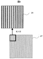
従来は、面方位(110)の半導体基板上の凹凸の溝パターンを、図6に示すように一定方向の回折格子パターン28としてレーザ干渉露光法と湿式エッチングにより作製していた。回折格子28のピッチ寸法は約200nmであり、この値はレーザを用いた回折角測定により求められている。回折格子パターン28は、4mm角の標準部材基板27の全面に一様に形成されている。この部材を用いて電子ビーム測長装置を校正する場合には、以下の問題がある。
Conventionally, a concave / convex groove pattern on a semiconductor substrate having a plane orientation (110) has been produced by a laser interference exposure method and wet etching as a
まず、第1の問題が微細性である。最新の半導体パターンでは最小加工寸法が100nmを切るものが現れてきている。しかしながら、レーザ干渉露光による従来の回折格子パターンでは最小ピッチ寸法は200nmであり、半導体パターンを測長する二十万倍以上の画像視野には回折格子パターンの1ピッチ分が入りきらなくなるために、この倍率での寸法校正ができなくなった。第2の問題は試料全体が一様なパターンであるため校正位置の特定ができないことである。このために試料内の複数点を測長し、その平均を求めるために校正に時間がかかった。また、面方位(110)の半導体基板上の凹凸パターンでは一方向の回折格子しか作製ができない。このために一方向のみの寸法校正しかできない欠点があった。 First, the first problem is fineness. Some of the latest semiconductor patterns have a minimum processing dimension of less than 100 nm. However, in the conventional diffraction grating pattern by laser interference exposure, the minimum pitch dimension is 200 nm, and one pitch of the diffraction grating pattern cannot be included in the image field of 200,000 times or more for measuring the semiconductor pattern. Dimension calibration at this magnification is no longer possible. The second problem is that the calibration position cannot be specified because the entire sample has a uniform pattern. For this reason, it took time to calibrate in order to measure a plurality of points in the sample and obtain the average. In addition, the concavo-convex pattern on the semiconductor substrate with the plane orientation (110) can only produce a diffraction grating in one direction. For this reason, there has been a drawback that only one-direction dimension calibration is possible.
これに対して、本発明では、パターン露光方法として電子ビーム一括露光法を用い、エッチングにはドライエッチングを用いた。この方法では、ピッチ寸法100nm以下のパターニングが可能であるが、このピッチ寸法の回折格子では、波長限界のため絶対寸法としてその波長が値付けされているレーザ光による光学的回折角測定が困難であった。 On the other hand, in the present invention, the electron beam batch exposure method is used as the pattern exposure method, and the dry etching is used for the etching. With this method, patterning with a pitch dimension of 100 nm or less is possible, but with a diffraction grating with this pitch dimension, it is difficult to measure the optical diffraction angle with a laser beam whose wavelength is priced as an absolute dimension because of the wavelength limit. there were.
そこで、図1に示すような回折格子パターンを標準部材基板5の校正用パターン領域3に作製した。この回折格子パターンは、長さ2μm、ピッチ200nmで直線溝が10本並んだ回折格子単位パターン1が、縦方向に2.5μmピッチ、横方向に2.4μmピッチで配列されている。この配列の一部に、図のように長さ2μm、ピッチ100nmで直線溝が20本並んだ回折格子単位パターン2が配置されている。また、校正用パターン領域3の周辺には、測長に使用するプローブ手段の位置決め用の十字マーク400、401が配置されている。標準部材には、これらのパターンを含んだ5mm角の標準部材基板5と上記回折格子単位パターンの直線溝を縦方向(もしくは、横方向)に配列させた格子配列を含んだ校正用パターン領域が配置されている。
Therefore, a diffraction grating pattern as shown in FIG. 1 was prepared in the
この標準部材に、波長が絶対寸法として保証されているHe−Cdレーザを照射して回折角を測定することにより、ピッチ200nmで10本の回折格子単位パターン1のピッチ寸法が200.01nmであることが精度0.01 nmで値付けられた。また、ピッチ100nmで直線溝が20本並んだ回折格子単位パターン2のピッチ寸法は、走査型プローブ顕微鏡(例えば、AFM)を用いて以下のように求め、100.45nmと値が得られた。まず、回折格子単位パターンを探すために位置決め用の十字マーク400、401を用いて標準部材と走査型プローブ顕微鏡の移動方向の平行性を補正し、各回折格子単位への位置決めが2μm以下になるようにする。次に、配列内のピッチ200nmで10本の回折格子単位パターン1のピッチ寸法を測長し、この値を200.01nmとすることで走査型プローブ顕微鏡の寸法校正を行った後、回折格子単位パターン2のピッチ寸法を測定する。回折格子単位パターン2は長さが2μmあるので100%の正しさで走査型プローブ顕微鏡の走査を回折格子単位パターンに位置決めでき、そのピッチ寸法を19ピッチ分の測定から求めることができた。同様にして、20点以上の異なる回折格子単位パターン2のピッチ寸法を求め、その平均値として100.45nmが得られた。
By irradiating this standard member with a He—Cd laser whose wavelength is guaranteed as an absolute dimension and measuring the diffraction angle, the pitch dimension of 10 diffraction
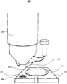
次に、この測長用標準部材を用いた電子ビーム測長装置の校正について説明する。50nm設計寸法のデバイスパターンが含まれた試料ウェーハ32とホルダー34に取り付けられた標準部材35が、図7のように電子ビーム測長装置のステージ33に搭載されている。50nm設計寸法のデバイスパターンを測長する場合には、電子ビーム測長装置の倍率を20万倍以上で行う。この倍率で従来の寸法標準であるピッチ200nmの回折格子では電子光学系29により絞られた電子ビーム30の走査の中に1ピッチが入らなくなってしまうので装置の校正ができない。
Next, calibration of the electron beam length measuring apparatus using this length measuring standard member will be described. A
この倍率の校正については、電子ビーム測長装置にて回折格子単位パターン2のピッチ寸法を測定する。まず、ピッチ100nmで直線溝が20本並んだ回折格子単位パターン2を探すために位置決め用の十字マーク400、401を用いて試料と電子ビーム測長装置の移動方向の平行性を補正する。次に、配列内の回折格子単位パターン2のピッチ寸法を二次電子信号検出器31からの二次電子信号波形で測定する。同様にして、20点以上の異なる回折格子単位パターン2のピッチ寸法を求め、その平均値を100.45nmとすることで校正ができた。
For this magnification calibration, the pitch dimension of the diffraction
この校正の正しさを確認するために、配列内のピッチ200nmで10本の回折格子単位パターン1のピッチ寸法を1ピッチが走査範囲に入る倍率である10万倍にして測長し、200.06nmを得た。この標準部材では、ピッチ100nmで直線溝が20本並んだ回折格子単位パターン2と、ピッチ200nmで10本の回折格子単位パターン1との距離は2.5μmであり、電子ビーム測長装置の電子光学系29のフォーカス条件を変更しない状態で測長ができる範囲である20μm以内であることから、高精度な校正が実現できる。その結果、回折角の測定から得られたピッチ寸法200.01nmとの差異が0.05nmとなり、良好な結果が得られた。
In order to confirm the correctness of the calibration, the pitch dimension of 10 diffraction
次に、本発明による測長用標準部材の作製方法について述べる。まず、Si基板上に100nm以下の酸化膜を形成後、レジストを表面に塗布する。次に、図8に示した作製フローにより、図9に示した開口10、11を有したステンシルマスクを搭載した電子ビーム一括露光装置でパターン形成を行った。
Next, a method for producing a length measuring standard member according to the present invention will be described. First, after forming an oxide film of 100 nm or less on a Si substrate, a resist is applied to the surface. Next, according to the manufacturing flow shown in FIG. 8, pattern formation was performed by an electron beam batch exposure apparatus equipped with a stencil
ビーム偏向により校正用パターンのひとつであるピッチ200nmで10本の回折格子単位パターンに相当する開口38を選択して上記試料上の所望の位置にビーム偏向により露光する(ステップ81)。この描画の照射量(ドーズ)は、ピッチ200nmで10本の回折格子単位パターン解像に適した10μC/cm2とした(ステップ82)。
An
次に、ビーム偏向により校正用パターンのもうひとつのパターンであるピッチ100nmで直線溝が20本並んだ回折格子単位パターンに相当する開口40を選択して、上記試料上の所望の位置にビーム偏向により露光する(ステップ83)。この描画の照射量は、ピッチ100nmで直線溝が20本並んだ回折格子単位パターン解像に適した15μC/cm2とした(ステップ84)。
Next, an
次に、可変成形用矩形開口36を用いて回折格子パターンが露光されている周囲の左右に試料回転補正用のマーク400、401を電子ビーム可変成形法で露光する(ステップ85)。この描画の照射量は、マークパターン解像に適した7μC/cm2とした(ステップ86)。 Next, the sample rotation correction marks 400 and 401 are exposed by the electron beam variable shaping method on the left and right sides of the periphery where the diffraction grating pattern is exposed using the variable shaping rectangular opening 36 (step 85). The irradiation dose for this drawing was set to 7 μC / cm 2 suitable for mark pattern resolution (step 86).
同様にして、横方向の回折格子パターンについても描画を行った。ビーム偏向により校正用パターンのひとつであるピッチ200nmで10本の回折格子単位パターンに相当する開口37を選択して、上記試料上の所望の位置にビーム偏向により、横方向の回折格子パターンを露光する。この描画の照射量は、ピッチ200nmで10本の回折格子単位パターン解像に適した10μC/cm2とした。次に、ビーム偏向により校正用パターンのもうひとつのパターンであるピッチ100nmで直線溝が20本並んだ回折格子単位パターンに相当する開口39を選択して上記試料上の所望の位置にビーム偏向により露光する。この描画の照射量はピッチ100nmで直線溝が20本並んだ回折格子単位パターン解像に適した15μC/cm2とした。
Similarly, drawing was also performed for the diffraction grating pattern in the horizontal direction. An
現像後、レジストをマスクとして酸化膜をエッチングし、次にドライエッチングにより、Si基板をエッチングする(ステップ87)。 After development, the oxide film is etched using the resist as a mask, and then the Si substrate is etched by dry etching (step 87).
描画では、上記のように電子ビーム露光において回折格子パターンの方向を縦・横両方向を同一基板上に作製しておく。回折格子パターンとして電子ビーム一括露光方を用いることにより、試料のどの位置でも同じステンシルマスクを用いて露光するために寸法バラツキ5nm以下の均一なパターン形成が可能であった。 In drawing, as described above, the direction of the diffraction grating pattern in both the vertical and horizontal directions is prepared on the same substrate in the electron beam exposure. By using the electron beam batch exposure method as the diffraction grating pattern, it was possible to form a uniform pattern with a dimensional variation of 5 nm or less because exposure was performed using the same stencil mask at any position of the sample.
なお、図1に示すようなパターンの実施例においては、各回折格子間の距離を短くとることができるので、SEMでの値付けが正確にできるという利点を有する。 In the embodiment of the pattern as shown in FIG. 1, since the distance between the diffraction gratings can be shortened, there is an advantage that the SEM can be accurately priced.
図2に、本発明による測長用標準部材の別の実施例を示す。図2では、回折格子パターンは、長さ2μm、ピッチ200nmで10本の回折格子単位パターン6が、縦方向に2.5μmピッチ、横方向に2.4μmピッチで2mm角の校正用パターン領域8に配列されている。この領域の近傍に、図のように長さ2μm、ピッチ100nmで直線溝が20本並んだ回折格子単位パターン7を2mm角の校正用パターン領域9に配列させたものを配置した。また、上記回折格子パターンの周辺には、位置決め用の十字マーク100、101が配置されている。
FIG. 2 shows another embodiment of the length measuring standard member according to the present invention. In FIG. 2, the diffraction grating pattern has a length of 2 μm, 10 diffraction grating unit patterns 6 at a pitch of 200 nm, a calibration pattern region 8 having a 2.5 μm pitch in the vertical direction and a 2 mm square at a pitch of 2.4 μm in the horizontal direction. Is arranged. In the vicinity of this region, a diffraction
標準部材基板5には、これらのパターンのほかに、図示のように上記回折格子単位の直線を横方向に配列させた格子配列を含んだ2mm角の校正用パターン領域11、12がそれぞれ配置されている。図3に、その詳細を示す。校正用パターン領域11、12には、回折格子単位パターン13、14が、それぞれ回折格子単位パターン6、7と同じ長さ、同じピッチで横方向に配列されている。
In addition to these patterns, the
この標準部材のピッチ200nmで10本の回折格子単位パターン6が縦方向に2.5μmピッチ、横方向に2.4μmピッチで配列された2mm角の領域に波長が絶対寸法として保証されているHe−Cdレーザを照射して回折角を測定することにより、回折格子単位パターン6のピッチ寸法が200.02nmであることが精度0.01nmで値付けられた。また、ピッチ100nmで直線溝が20本並んだ回折格子単位パターン7のピッチ寸法は、波長193nmの極紫外固体レーザによる回折角測定により100.40nmの値が得られた。この測定では、まずピッチ200nmで10本の回折格子単位パターン6のピッチ寸法を同じ波長193nmの極紫外固体レーザによる回折角測定により測定し、波長が絶対寸法として保証されているHe−Cdレーザを照射して回折角を測定することにより200.02nmの値が得られた。これにより、波長193nmの極紫外固体レーザによる回折角測定が校正されている。
The wavelength is guaranteed as an absolute dimension in a 2 mm square region in which 10 diffraction grating unit patterns 6 are arranged with a pitch of 200 μm and a pitch of 2.5 μm in the vertical direction and a pitch of 2.4 μm in the horizontal direction. By irradiating the -Cd laser and measuring the diffraction angle, the pitch dimension of the diffraction grating unit pattern 6 was determined to be 200.02 nm with an accuracy of 0.01 nm. Further, the pitch dimension of the diffraction
次に、この測長用標準部材を用いた電子ビーム測長装置の校正について説明する。50nm設計寸法のデバイスパターンが含まれた試料ウェーハ32と標準部材が、図7のように電子ビーム測長装置に搭載されている。50nm設計寸法のデバイスパターンを測長する場合には、電子ビーム測長装置の倍率を20万倍以上で行う。この倍率で従来の寸法標準であるピッチ200nmの回折格子では電子ビーム走査の中に1ピッチが入らなくなってしまうので装置の校正ができない。
Next, calibration of the electron beam length measuring apparatus using this length measuring standard member will be described. A
この倍率の校正については、電子ビーム測長装置にて回折格子単位パターン7のピッチ寸法を測定する。まず、ピッチ100nmで直線溝が20本並んだ回折格子単位パターン7を探すために位置決め用の十字マーク100、101を用いて試料と電子ビーム測長装置の移動方向の平行性を補正する。次に、配列内の回折格子単位パターン7のピッチ寸法を測定する。同様にして、20点以上の異なる回折格子単位パターン7のピッチ寸法を求めその平均値を100.40nmとすることで校正ができた。この校正の正しさを確認するために、配列内のピッチ200nmで10本の回折格子単位パターン6のピッチ寸法を1ピッチが走査範囲に入る倍率である10万倍にして測長し、200.08nmを得た。回折角の測定から得られたピッチ寸法200.02nmとの差異が0.06nmと良好な結果が得られた。同様に、図3に示したように同じ標準部材パターンに作りこんだ横方向のピッチ100nmで直線溝が20本並んだ回折格子単位パターン14の配列およびピッチ200nmで10本の回折格子単位パターン13の配列によって、横方向の電子ビーム測長装置の測長寸法校正が高精度に実現できた。
For this magnification calibration, the pitch dimension of the diffraction
なお、図2、図3に示すようなパターンの実施例においては、各校正用パターン領域が分かれているので、ピッチ寸法の大きい方のパターンを光回折で、ピッチ寸法の小さい方のパターンも光回折で値付けできるという利点を有する。 In the embodiment of the pattern as shown in FIGS. 2 and 3, since each calibration pattern area is separated, the pattern with the larger pitch dimension is optically diffracted, and the pattern with the smaller pitch dimension is also light. It has the advantage that it can be priced by diffraction.
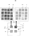
図4に、本発明による測長用標準部材のさらに別の実施例を示す。図4では、回折格子パターンは、長さ2μm、ピッチ200nmで10本の回折格子単位パターン15が縦方向に2.5μmピッチ、横方向に2.4μmピッチで2mm角の校正用パターン領域17に配列されている。この領域の近傍に、図のように長さ2μm、ピッチ100nmで直線溝が4本並んだ回折格子単位パターン16、161を2mm角の校正用パターン領域18に配列させたものを配置した。これらの4本並んだ回折格子単位パターンから横に2μm離れた位置には、それぞれの回折格子単位パターンの位置を特定できる一つ一つ形の異なるマークパターン160、162がそれぞれ位置されている。また、上記回折格子パターンの周辺には位置決め用の十字マーク102、103が配置されている。
FIG. 4 shows still another embodiment of the length measuring standard member according to the present invention. In FIG. 4, the diffraction grating pattern has a length of 2 μm, a pitch of 200 nm, 10 diffraction
この標準部材基板5には、これらのパターンのほかに上記回折格子単位パターン15の直線溝を横方向に配列させた格子配列を含んだ2mm角の校正用パターン領域19、20が、それぞれ配置されている。
In addition to these patterns, the
この標準部材のピッチ200nmで10本の回折格子単位パターン15が縦方向に2.5μmピッチ、横方向に2.4μmピッチで配列された2mm角の領域に波長が絶対寸法として保証されているHE−Cdレーザを照射して回折角を測定することにより回折格子単位パターン15のピッチ寸法が200.01nmであることが精度0.01nmで値付けられた。また、ピッチ100nmで直線溝が4本並んだ回折格子単位パターン16の中央部のピッチ寸法は、走査型プローブ顕微鏡を用いて、以下のように求め、100.55nmおよび100.65nmと値が得られた。
HE whose wavelength is guaranteed as an absolute dimension in a 2 mm square region in which 10 diffraction
まず、回折格子単位パターンを探すために位置決め用の十字マーク102、103を用いて試料と走査型プローブ顕微鏡の移動方向の平行性を補正し、各回折格子単位への位置決めが2μm以下になるようにする。次に、配列内のピッチ200nmで10本の回折格子単位パターン15のピッチ寸法を測長しこの値を200.01nmとすることで走査型プローブ顕微鏡の寸法校正を行った後、回折格子単位パターン16の中央部のピッチ寸法をそれぞれ測定する。回折格子単位パターン16は長さが2μmあるので100%の正しさで走査型プローブ顕微鏡の走査を回折格子単位パターンに位置決めできた。また、それぞれの測定した回折格子パターンの位置は近傍に有るマークパターン160を走査することにより判別が可能であった。
First, in order to find the diffraction grating unit pattern, the parallelism in the moving direction of the sample and the scanning probe microscope is corrected using the positioning cross marks 102 and 103 so that the positioning to each diffraction grating unit is 2 μm or less. To. Next, after measuring the pitch dimension of 10 diffraction
次に、この測長用標準部材を用いた電子ビーム測長装置の校正について説明する。この電子ビーム測長装置は、図12に示すような装置構成となっており、図11に示すような手順で校正が行われるように校正プログラムが組まれており、これに則って校正を行った。測定では、電子銃41から照射される電子ビーム42をレンズ43、45により細く絞り、偏向器44によりステージ47上に搭載された試料46上で走査するとき発生する二次電子48を二次電子検出器49により検出し、ビーム偏向制御部と二次電子信号処理部から波形を求める。この波形から寸法を演算し寸法校正演算により正しい寸法として寸法表示および記憶する。本発明の電子ビーム測長装置では、図12に示すように、さらに校正比較のために基準値との差分演算部と校正状態表示部があり、異なる基準寸法での比較により校正の正しさが得られ、それを表示できるようになっている。
Next, calibration of the electron beam length measuring apparatus using this length measuring standard member will be described. This electron beam length measuring device has a configuration as shown in FIG. 12, and a calibration program is set up so that calibration is performed according to the procedure shown in FIG. 11, and calibration is performed in accordance with this. It was. In the measurement, the
実際の測定について、以下に説明する。50nm設計寸法のデバイスパターンが含まれた試料ウェーハ32と標準部材が、図7のように電子ビーム測長装置に搭載されている。50nm設計寸法のデバイスパターンを測長する場合には、電子ビーム測長装置の倍率を20万倍以上で行う。この倍率では、従来の寸法標準であるピッチ200nmの回折格子を用いると電子ビーム走査の中に1ピッチが入らなくなってしまうので装置の校正ができない。
The actual measurement will be described below. A
この倍率の校正については、図11の手順に従って行なう。電子ビーム測長装置にて回折格子単位パターン16のピッチ寸法を測定する。まず、値付けされたピッチ100nmで直線溝が4本並んだ回折格子単位パターン16を探すために位置決め用の十字マーク102、103を用いて試料と電子ビーム測長装置の移動方向の平行性を補正する。次に、配列内のマークパターン160を基に値付けされた回折格子単位パターン16のピッチ寸法を、ビーム偏向制御部と二次電子信号処理部から得られた波形表示および寸法演算により寸法表示およびその寸法を寸法記憶部に記憶することで測定する。そのピッチ値を100.55nmとなるように寸法校正演算部で校正し、その寸法を記憶部に格納することにより校正ができた(ステップ111)。
This magnification calibration is performed according to the procedure shown in FIG. The pitch dimension of the diffraction
校正の正しさを確認するために、この配列内のピッチ200nmで10本の回折格子単位パターン1のピッチ寸法を1ピッチが走査範囲に入る倍率である10万倍にして、図12の構成に従い校正された寸法校正演算部を通して測長し、200.03nmを得た(ステップ112)。回折角の測定から得られたピッチ寸法200.01nmとの差異が0.02nmとなった。この差分が基準値として設定した0.1nm以下であったので(ステップ113)、基準値との差分演算部から校正状態表示部へ正常の表示が出され、良好な測長が保証された(ステップ114)。同様に、図4に示したように同じ標準部材パターンに作りこんだ横方向のピッチ100nmで直線が4本並んだ回折格子単位パターン配列20およびピッチ200nmで10本の回折格子単位パターン配列19によって横方向の電子ビーム測長装置の測長寸法校正が高精度に実現できた。
In order to confirm the correctness of the calibration, the pitch dimension of 10 diffraction
次に、かかる校正を3ヶ月後に上記と同様に同じ回折格子パターンを用いて行った。まず、値付けされたピッチ100nmで直線溝が4本並んだ回折格子単位パターン16を探すために位置決め用の十字マーク102、103を用いて試料と電子ビーム測長装置の移動方向の平行性を補正し、次に配列内のマークパターン160を基に今までと同じ位置に有る値付けされた回折格子単位パターン16のピッチ寸法を測定した。そのピッチ値を100.55nmとすることで校正ができた。
Next, such calibration was performed after three months using the same diffraction grating pattern as described above. First, in order to search for the diffraction
この校正の正しさを確認するために、配列内のピッチ200nmで10本の回折格子単位パターン15のピッチ寸法を1ピッチが走査範囲に入る倍率である10万倍にして測長したところ、200.25nmとなり、回折角の測定から得られたピッチ寸法200.01nmとの差異が0.24nmと、校正の基準として設定した0.1nmを超えたために、基準値との差分演算部から電子ビーム測長装置の校正状態表示部へ異常の表示が出された(ステップ115)。
In order to confirm the correctness of the calibration, the pitch dimension of 10 diffraction
このために、図11の手順に従い、上記とは別の位置に有り値付けされたピッチ100nmで直線が4本並んだ回折格子単位パターン161をマークパターン162を基に特定し、そのピッチ寸法を測定し100.65nmとすることで校正ができた(ステップ111)。この校正の正しさを確認するために、配列内のピッチ200nmで10本の回折格子単位パターン15のピッチ寸法を1ピッチが走査範囲に入る倍率である10万倍にして測長し、200.02nmを得た(ステップ112)。回折角の測定から得られたピッチ寸法200.01nmとの差異が0.01nmと良好な結果が得られ(ステップ113)、高精度な校正が維持され安定した測長性能が継続できた(ステップ114)。
For this purpose, according to the procedure of FIG. 11, a diffraction
これに対し、図10に示すような構成の従来の電子ビーム測長装置および図6に示すような従来の校正パターン28を用いた装置校正では、上記のように数ヶ月以上の長期的な運用において校正パターン28を何回も使用するために、電子ビーム照射による汚染によって校正パターンの寸法変動が起こった場合には、複数の寸法基準との比較や校正状態の良否を表示する機能がないためにその精度を保証できないという問題があった。
In contrast, in the conventional electron beam length measuring apparatus having the configuration shown in FIG. 10 and the apparatus calibration using the
なお、図4に示すようなパターンの実施例においては、ピッチ寸法の小さい方のパターンの位置が特定できるので、AFM等による測定が容易であるという利点を有する。 In the embodiment of the pattern as shown in FIG. 4, since the position of the pattern having the smaller pitch dimension can be specified, there is an advantage that measurement by AFM or the like is easy.
図5に、本発明による測長用標準部材のさらに別の実施例を示す。図5では、回折格子パターンは、長さ2μm、ピッチ200nmで10本の回折格子単位パターン21が、縦方向に2.5μmピッチ、横方向に2.4μmピッチで2mm角の校正用パターン領域23に配列されている。この配列の一部に、図のようにピッチ200nmで横方向の直線溝が10本の回折格子単位パターン210が配置されている。この領域の近傍に、図のように長さ2μm、ピッチ100nmで直線溝が20本並んだ回折格子単位パターン22を2mm角の校正用パターン領域24に配列させたものを配置した。この配列の一部に、図5のようにピッチ100nmで横方向の直線溝が20本の回折格子単位パターン220が配置されている。また、上記回折格子パターン1の周辺には位置決め用の十字マーク104、105が配置されている。
FIG. 5 shows still another embodiment of the length measuring standard member according to the present invention. In FIG. 5, the diffraction grating pattern has a length of 2 μm, 10 diffraction
この標準部材のピッチ200nmで10本の回折格子単位パターン21、210が、縦方向に2.5μmピッチ、横方向に2.4μmピッチで配列された2mm角の校正用パターン領域23に波長が絶対寸法として保証されているHe−Cdレーザを照射して回折角を測定することにより回折格子単位パターン21、210のピッチ寸法が両方とも200.02nmであることが精度0.01nmで値付けられた。また、ピッチ100nmで直線溝が20本並んだ回折格子単位パターン22、220のピッチ寸法は、波長193nmの極紫外固体レーザによる回折角測定により両方とも100.40nmの値が得られた。この測定では、まずピッチ200nmで10本の回折格子単位パターン21、210のピッチ寸法を同じ波長193nmの極紫外固体レーザによる回折角測定により測定し、波長が絶対寸法として保証されているHe−Cdレーザを照射して回折角を測定することにより200.02nmが得られた。これにより、波長193nmの極紫外固体レーザによる回折角測定が校正されている。
The standard member has a pitch of 200 nm and 10 diffraction
次に、この試料を用いた電子ビーム測長装置の校正について説明する。50nm設計寸法のデバイスパターンが含まれた試料ウェーハ32と標準部材が図7のように電子ビーム測長装置に搭載されている。50nm設計寸法のデバイスパターンを測長する場合には、電子ビーム測長装置の倍率を20万倍以上で行う。この倍率で、従来の寸法標準であるピッチ200nmの回折格子では電子ビーム走査の中に1ピッチが入らなくなってしまうので装置の校正ができない。
Next, calibration of the electron beam length measuring apparatus using this sample will be described. A
この倍率の校正については、電子ビーム測長装置にて回折格子単位パターン22のピッチ寸法を測定する。まず、ピッチ100nmで直線溝が20本並んだ回折格子単位パターン22を探すために位置決め用の十字マーク104、105を用いて試料と電子ビーム測長装置の移動方向の平行性を補正する。次に、配列内の回折格子単位パターン22のピッチ寸法を測定する。同様にして、20点以上の異なる回折格子単位パターンのピッチ寸法を求めその平均値を100.40nmとすることで校正ができた。この校正の正しさを確認するために配列内のピッチ200nmで10本の回折格子単位パターン21のピッチ寸法を1ピッチが走査範囲に入る倍率である10万倍にして測長し、200.08nmを得た。回折角の測定から得られたピッチ寸法200.02nmとの差異が0.06nmと良好な結果が得られた。同様に、同じ標準部材パターンに作りこんだ横方向のピッチ100nmで直線溝が20本並んだ回折格子単位パターン220配列およびピッチ200nmで10本の回折格子単位パターン210配列によって横方向の電子ビーム測長装置の測長寸法校正が0.1nm以内の高精度で実現できた。これらの縦方向と横方向の回折格子単位との距離は2.5μmと電子ビーム測長装置のフォーカス条件を変更しない状態で測長ができる範囲である20μm以内であることから、縦横両方の方向で高精度な校正が実現できた。
For this magnification calibration, the pitch dimension of the diffraction
なお、図5に示すようなパターンの実施例においては、特に、縦・横方向が近接しているので、縦・横方向の校正が高精度にできるという利点を有する。 In the embodiment of the pattern as shown in FIG. 5, since the vertical and horizontal directions are close to each other, there is an advantage that calibration in the vertical and horizontal directions can be performed with high accuracy.
以上説明した各実施例において、校正用標準部材は、図7のようにホルダー34にパターニングされた半導体基板35を貼り付けたものについて説明したが、パターニングされた半導体基板が測定したいウェーハ32と同じウェーハ形状であっても、校正時に校正用標準部材ウェーハを搭載して装置を校正後、測定したいウェーハ32と交換して測定すれば高精度測長が可能である。
In each of the embodiments described above, the standard member for calibration has been described in which the patterned
また、上述した実施例では、図2〜図5のように、回折格子単位パターンの直線溝を縦方向、横方向に配列させた格子配列の場合について説明したが、本発明は、これらの格子配列に限らず、回折格子単位パターンの直線溝の方向が互いに異なる方向に配列された格子配列に対しても適用可能であることはいうまでもない。 Further, in the above-described embodiment, the case of the grating arrangement in which the linear grooves of the diffraction grating unit pattern are arranged in the vertical direction and the horizontal direction as shown in FIGS. 2 to 5 has been described. Needless to say, the present invention can be applied not only to the arrangement but also to a grating arrangement in which the directions of the linear grooves of the diffraction grating unit pattern are different from each other.
以上、本発明によれば、波長が絶対的に保証されているレーザ光を用いた光学的回折角により値付けされるピッチ寸法以下の寸法校正でも対応が可能となる。また、波長が絶対的に保証されているレーザ光を用いた光学的回折角により値付けされるピッチ寸法とそれよりも微細な基準パターンを設け、両方の基準寸法を比較することにより校正が適正なものであるとの保証が実現でき、安定した高精度電子ビーム測長が可能となる。また、二つの直交したパターンを同一基板中に配置することで縦・横の方向のパターンについての測長の高精度校正ができる。 As described above, according to the present invention, it is possible to cope with a dimensional calibration of a pitch dimension or less that is priced by an optical diffraction angle using a laser beam whose wavelength is absolutely guaranteed. In addition, the pitch dimension determined by the optical diffraction angle using laser light whose wavelength is absolutely guaranteed and a finer reference pattern are provided, and the calibration is appropriate by comparing both reference dimensions. It is possible to guarantee that the sensor is safe, and it is possible to perform stable high-precision electron beam length measurement. In addition, by arranging two orthogonal patterns on the same substrate, it is possible to perform high-precision calibration of length measurement for patterns in the vertical and horizontal directions.
1、2、6、7、13、14、15、16、161、21、22、210、220、28…回折格子パターン、400、401、100、101、102、103、104、105…位置検出用十字パターン、3、8、9、11、12、17、18、19、20、23、24、25、26…校正用パターン領域、5、27、35…標準部材基板、29…電子光学系、30、42…電子ビーム、31、49…二次電子検出器、32、46…ウェーハ、33、47…ステージ、34…ホルダー、36…可変成形用矩形開口、37、38、39、40…回折格子パターン用開口、41…電子銃、43、45…レンズ、44…偏向器、48…二次電子。
1, 2, 6, 7, 13, 14, 15, 16, 161, 21, 22, 210, 220, 28 ... diffraction grating pattern, 400, 401, 100, 101, 102, 103, 104, 105 ... position
Claims (9)
前記第1の回折格子単位パターンよりもピッチ寸法の小さい回折格子の配列よりなる第2の回折格子単位パターンとを含み、
前記第1の回折格子単位パターンが2次元で前記回折格子の格子溝に対して横方向、縦方向のそれぞれに等ピッチで配列されており、前記第1の回折格子単位パターンの配列の一部が前記第2の回折格子単位パターンで置換された構成を有することを特徴とする測長用標準部材。 A first diffraction grating unit pattern consisting of an array of diffraction gratings whose pitch dimension is previously determined by optical means on the substrate;
A second diffraction grating unit pattern consisting of an array of diffraction gratings having a smaller pitch dimension than the first diffraction grating unit pattern,
The first diffraction grating unit patterns are two-dimensionally arranged at equal pitches in the horizontal and vertical directions with respect to the grating grooves of the diffraction grating, and a part of the arrangement of the first diffraction grating unit patterns A standard member for length measurement, having a configuration in which is replaced with the second diffraction grating unit pattern.
ッチ寸法が、100nm以下であることを特徴とする測長用標準部材。 2. The length measuring standard member according to claim 1, wherein a minimum pitch dimension of the second diffraction grating unit pattern is 100 nm or less.
前記第1の回折格子単位パターンよりもピッチ寸法の小さい回折格子の配列よりなる第2の回折格子単位パターンを複数配置した第2のパターン領域とを備え
前記第2のパターン領域が、前記第1のパターン領域の近傍に配置されてなることを特徴とする測長用標準部材。 On the substrate, a first diffraction grating unit pattern composed of an array of diffraction gratings whose pitch dimensions have been obtained in advance by optical means is two-dimensionally arranged in a lateral direction and a longitudinal direction with respect to the grating grooves of the diffraction grating. A plurality of first pattern regions arranged at equal pitches;
A second pattern region in which a plurality of second diffraction grating unit patterns each having a pitch dimension smaller than that of the first diffraction grating unit pattern are arranged. The second pattern region includes the first pattern region. A standard member for length measurement, which is arranged in the vicinity of the pattern area.
段の位置決め用マークパターンを備えたことを特徴とする測長用標準部材。 2. The standard member for length measurement according to claim 1, wherein a positioning mark pattern of probe means used for length measurement is provided on the substrate.
2の回折格子単位パターンの各々の位置情報を含む複数のマークパターンを含むことを特
徴とする測長用標準部材。 5. The standard member for length measurement according to claim 4, wherein the second pattern region includes a plurality of mark patterns including position information of each of the plurality of second diffraction grating unit patterns. Standard member for long.
前記試料ステージ上の試料に対して電子ビームを走査する照射光学系と、
前記電子ビーム走査により発生する二次電子線を検出する二次電子検出器と、
前記検出器から得られる信号波形を解析することにより前記試料を測長する演算処理手段と、
測長結果が表示される表示手段と、
前記試料ステージ上に保持された測長用標準部材とを有し、
前記測長用標準部材は、
基板上に、光学的手段により予めピッチ寸法が求められている回折格子の配列よりなる第1の回折格子単位パターンと、前記第1の回折格子単位パターンよりもピッチ寸法の小さい複数の回折格子の配列よりなる第2の回折格子単位パターンとを備え、
前記第1の回折格子単位パターンが2次元で前記回折格子の格子溝に対して横方向、縦方向のそれぞれに等ピッチで配列されており、前記第1の回折格子単位パターンの配列の一部が前記第2の回折格子単位パターンで置換された構成を有することを特徴とする電子ビーム測長装置。 A sample stage for holding the sample;
An irradiation optical system for scanning an electron beam with respect to a sample on the sample stage;
A secondary electron detector for detecting a secondary electron beam generated by the electron beam scanning;
Arithmetic processing means for measuring the length of the sample by analyzing a signal waveform obtained from the detector;
Display means for displaying the measurement results;
A standard member for length measurement held on the sample stage,
The standard member for length measurement is
On the substrate, a first diffraction grating unit pattern having an arrangement of diffraction gratings whose pitch dimension is previously determined by optical means, and a plurality of diffraction gratings having a pitch dimension smaller than that of the first diffraction grating unit pattern. A second diffraction grating unit pattern comprising an array,
The first diffraction grating unit patterns are two-dimensionally arranged at equal pitches in the horizontal and vertical directions with respect to the grating grooves of the diffraction grating, and a part of the arrangement of the first diffraction grating unit patterns The electron beam length-measuring device has a configuration in which is replaced with the second diffraction grating unit pattern.
前記試料ステージ上の試料に対して電子ビームを走査する照射光学系と、
前記電子ビーム走査により発生する二次電子線を検出する二次電子検出器と、
前記検出器から得られる信号波形を解析することにより前記試料を測長する演算処理手段と、
測長結果が表示される表示手段と、
前記測長結果を校正するための基準寸法値が格納された記憶手段と、
前記試料ステージ上に保持された測長用標準部材とを有し、
前記記憶手段に格納した基準寸法値は、前記測長用標準部材から取得した基準寸法値であり、
当該測長用標準部材には、
基板上に、光学的手段により予めピッチ寸法が求められている回折格子の配列よりなる第1の回折格子単位パターンと、前記第1の回折格子単位パターンよりもピッチ寸法の小さい複数の回折格子の配列よりなる第2の回折格子単位パターンとが形成されており、
前記第1の回折格子単位パターンが2次元で前記回折格子の格子溝に対して横方向、縦方向のそれぞれに等ピッチで配列されており、前記第1の回折格子単位パターンの配列の一部が前記第2の回折格子単位パターンで置換された構成を有することを特徴とする電子ビーム測長装置。 A sample stage for holding the sample;
An irradiation optical system for scanning an electron beam with respect to a sample on the sample stage;
A secondary electron detector for detecting a secondary electron beam generated by the electron beam scanning;
Arithmetic processing means for measuring the length of the sample by analyzing a signal waveform obtained from the detector;
Display means for displaying the measurement results;
Storage means for storing a reference dimension value for calibrating the measurement result;
A standard member for length measurement held on the sample stage,
Reference dimension value stored in the storage means is a reference dimension value obtained from the length-measuring standard member,
In the standard member for length measurement,
On the substrate, a first diffraction grating unit pattern having an arrangement of diffraction gratings whose pitch dimension is previously determined by optical means, and a plurality of diffraction gratings having a pitch dimension smaller than that of the first diffraction grating unit pattern. A second diffraction grating unit pattern comprising an array is formed,
The first diffraction grating unit patterns are two-dimensionally arranged at equal pitches in the horizontal and vertical directions with respect to the grating grooves of the diffraction grating, and a part of the arrangement of the first diffraction grating unit patterns The electron beam length-measuring device has a configuration in which is replaced with the second diffraction grating unit pattern.
測長結果と前記ピッチ寸法の差の許容限界である基準値を格納する記憶手段をさらに有し、
前記差が前記基準値と比較して大きい場合には前記表示手段に異常が表示されることを特徴とする電子ビーム測長装置。 The electron beam length-measuring device according to claim 7 or 8,
Storage means for storing a reference value which is an allowable limit of the difference between the length measurement result and the pitch dimension ;
An electron beam length-measuring device, wherein an abnormality is displayed on the display means when the difference is larger than the reference value.
Priority Applications (3)
| Application Number | Priority Date | Filing Date | Title |
|---|---|---|---|
| JP2004049218A JP4401814B2 (en) | 2004-02-25 | 2004-02-25 | Standard member for length measurement and electron beam length measuring device |
| US11/028,219 US7078691B2 (en) | 2004-02-25 | 2005-01-04 | Standard reference for metrology and calibration method of electron-beam metrology system using the same |
| US11/481,973 US7358495B2 (en) | 2004-02-25 | 2006-07-07 | Standard reference for metrology and calibration method of electron-beam metrology system using the same |
Applications Claiming Priority (1)
| Application Number | Priority Date | Filing Date | Title |
|---|---|---|---|
| JP2004049218A JP4401814B2 (en) | 2004-02-25 | 2004-02-25 | Standard member for length measurement and electron beam length measuring device |
Publications (3)
| Publication Number | Publication Date |
|---|---|
| JP2005241328A JP2005241328A (en) | 2005-09-08 |
| JP2005241328A5 JP2005241328A5 (en) | 2006-12-14 |
| JP4401814B2 true JP4401814B2 (en) | 2010-01-20 |
Family
ID=34858240
Family Applications (1)
| Application Number | Title | Priority Date | Filing Date |
|---|---|---|---|
| JP2004049218A Expired - Fee Related JP4401814B2 (en) | 2004-02-25 | 2004-02-25 | Standard member for length measurement and electron beam length measuring device |
Country Status (2)
| Country | Link |
|---|---|
| US (2) | US7078691B2 (en) |
| JP (1) | JP4401814B2 (en) |
Families Citing this family (24)
| Publication number | Priority date | Publication date | Assignee | Title |
|---|---|---|---|---|
| JP4287671B2 (en) * | 2003-02-19 | 2009-07-01 | 株式会社日立ハイテクノロジーズ | Standard member for length measurement, method for producing the same, and electron beam length measuring device using the same |
| JP4194526B2 (en) * | 2004-05-14 | 2008-12-10 | 株式会社日立ハイテクノロジーズ | Charged particle beam adjustment method and charged particle beam apparatus |
| JP4276140B2 (en) * | 2004-06-25 | 2009-06-10 | 株式会社日立ハイテクノロジーズ | Scanning electron microscope and dimensional calibration sample |
| US7408154B2 (en) * | 2004-10-29 | 2008-08-05 | Hitachi High-Technologies Corporation | Scanning electron microscope, method for measuring a dimension of a pattern using the same, and apparatus for correcting difference between scanning electron microscopes |
| JP2006234588A (en) * | 2005-02-25 | 2006-09-07 | Hitachi High-Technologies Corp | Pattern measuring method and pattern measuring device |
| US8825444B1 (en) | 2005-05-19 | 2014-09-02 | Nanometrics Incorporated | Automated system check for metrology unit |
| JP4839127B2 (en) * | 2006-05-10 | 2011-12-21 | 株式会社日立ハイテクノロジーズ | Standard member for calibration, calibration method and electron beam apparatus using the same |
| JP2007328038A (en) * | 2006-06-06 | 2007-12-20 | Hitachi High-Technologies Corp | Dimension calibration sample for microscope |
| US7777884B2 (en) * | 2007-01-23 | 2010-08-17 | Taiwan Semiconductor Manufacturing Company, Ltd. | Method and system for optimizing sub-nanometer critical dimension using pitch offset |
| JP5361137B2 (en) * | 2007-02-28 | 2013-12-04 | 株式会社日立ハイテクノロジーズ | Charged particle beam measurement system |
| US7605907B2 (en) * | 2007-03-27 | 2009-10-20 | Asml Netherlands B.V. | Method of forming a substrate for use in calibrating a metrology tool, calibration substrate and metrology tool calibration method |
| US7788818B1 (en) * | 2007-10-02 | 2010-09-07 | Sandia Corporation | Mesoscale hybrid calibration artifact |
| SG153747A1 (en) * | 2007-12-13 | 2009-07-29 | Asml Netherlands Bv | Alignment method, alignment system and product with alignment mark |
| DE102008052006B4 (en) * | 2008-10-10 | 2018-12-20 | 3D-Micromac Ag | Method and device for the production of samples for transmission electron microscopy |
| JP4902806B2 (en) * | 2011-07-22 | 2012-03-21 | 株式会社日立ハイテクノロジーズ | Standard material for calibration |
| US8624199B2 (en) * | 2011-10-28 | 2014-01-07 | Fei Company | Sample block holder |
| US9490182B2 (en) * | 2013-12-23 | 2016-11-08 | Kla-Tencor Corporation | Measurement of multiple patterning parameters |
| JP6605276B2 (en) | 2015-09-28 | 2019-11-13 | 株式会社日立ハイテクノロジーズ | Measuring device, measuring device calibration method and calibration member |
| CN106483049B (en) * | 2016-11-01 | 2019-08-13 | 浙江省计量科学研究院 | A kind of non-contact self-checking device and method of the Hegman grind gage error of indication |
| US20200388462A1 (en) * | 2017-12-05 | 2020-12-10 | Asml Netherlands B.V. | Systems and methods for tuning and calibrating charged particle beam apparatus |
| CN109444472A (en) * | 2018-12-19 | 2019-03-08 | 中国电子科技集团公司第十三研究所 | Scanning electron microscope alignment pattern print and preparation method |
| CN109855572A (en) * | 2018-12-25 | 2019-06-07 | 中国电子科技集团公司第十三研究所 | For calibrating the line-spacing template and preparation method of optical profilometer roughness |
| CN111024016B (en) * | 2019-12-04 | 2021-10-15 | 中国电子科技集团公司第十三研究所 | Film thickness sample and preparation method of film thickness sample |
| CN116157708A (en) | 2020-07-20 | 2023-05-23 | 应用材料公司 | Optical device and method for metering optical device |
Family Cites Families (6)
| Publication number | Priority date | Publication date | Assignee | Title |
|---|---|---|---|---|
| US5422723A (en) * | 1992-09-21 | 1995-06-06 | Texas Instruments Incorporated | Diffraction gratings for submicron linewidth measurement |
| JP2544588B2 (en) | 1994-07-29 | 1996-10-16 | 株式会社日立製作所 | Calibration member for length measurement and manufacturing method thereof |
| JP2000232138A (en) | 1999-02-09 | 2000-08-22 | Hitachi Ltd | Semiconductor device, marking device and defect inspection apparatus therefor |
| JP3843671B2 (en) | 1999-10-29 | 2006-11-08 | 株式会社日立製作所 | Semiconductor device pattern inspection apparatus and defect inspection / defect analysis method thereof |
| US7289212B2 (en) * | 2000-08-24 | 2007-10-30 | Asml Netherlands B.V. | Lithographic apparatus, device manufacturing method and device manufacturing thereby |
| JP4287671B2 (en) | 2003-02-19 | 2009-07-01 | 株式会社日立ハイテクノロジーズ | Standard member for length measurement, method for producing the same, and electron beam length measuring device using the same |
-
2004
- 2004-02-25 JP JP2004049218A patent/JP4401814B2/en not_active Expired - Fee Related
-
2005
- 2005-01-04 US US11/028,219 patent/US7078691B2/en not_active Expired - Fee Related
-
2006
- 2006-07-07 US US11/481,973 patent/US7358495B2/en not_active Expired - Fee Related
Also Published As
| Publication number | Publication date |
|---|---|
| JP2005241328A (en) | 2005-09-08 |
| US7358495B2 (en) | 2008-04-15 |
| US20060289756A1 (en) | 2006-12-28 |
| US7078691B2 (en) | 2006-07-18 |
| US20050184234A1 (en) | 2005-08-25 |
Similar Documents
| Publication | Publication Date | Title |
|---|---|---|
| JP4401814B2 (en) | Standard member for length measurement and electron beam length measuring device | |
| US7595482B2 (en) | Standard component for length measurement, method for producing the same, and electron beam metrology system using the same | |
| JP3373754B2 (en) | Method of determining bias or overlay error on a substrate | |
| US7473502B1 (en) | Imaging tool calibration artifact and method | |
| US5902703A (en) | Method for measuring dimensional anomalies in photolithographed integrated circuits using overlay metrology, and masks therefor | |
| JP4839127B2 (en) | Standard member for calibration, calibration method and electron beam apparatus using the same | |
| JP4708856B2 (en) | Electron beam calibration method and electron beam apparatus | |
| US6764794B2 (en) | Photomask for focus monitoring | |
| JP4074240B2 (en) | Deflection distortion correction system, deflection distortion correction method, deflection distortion correction program, and semiconductor device manufacturing method | |
| JP4269393B2 (en) | Alignment mark and alignment method | |
| US5741614A (en) | Atomic force microscope measurement process for dense photoresist patterns | |
| JP2009071103A (en) | Exposing system and method of manufacturing semiconductor apparatus | |
| JP4902806B2 (en) | Standard material for calibration | |
| JP2009270988A (en) | Calculating method for overlap misalignment and manufacturing method for semiconductor device | |
| JP4287891B2 (en) | Standard member for length measurement and electron beam length measuring device using the same | |
| KR20000076936A (en) | Electron Beam Lithographing Method and Apparatus Thereof | |
| JP2009158720A (en) | Exposure apparatus and method of manufacturing device | |
| KR100700370B1 (en) | Method of Preparing a Substrate, Method of Measuring, Device Manufacturing Method, Lithographic Apparatus, Computer Program and Substrate | |
| JP3694669B2 (en) | Electron beam drawing device | |
| JP2007206333A (en) | Mask for measuring flare and method for measuring flare | |
| JP6492086B2 (en) | Method for measuring the position of a structure on a mask and thereby determining mask manufacturing errors | |
| JP4276892B2 (en) | Standard member for length measurement and calibration method for electron beam length measuring device | |
| Nakayama et al. | Novel CD-SEM calibration reference consisting of 100-nm pitch grating and positional identification mark | |
| JP6605276B2 (en) | Measuring device, measuring device calibration method and calibration member | |
| JP2001358054A (en) | Method for detecting dimensional error of beam for exposure and method for detecting illuminating positional error of beam for exposure |
Legal Events
| Date | Code | Title | Description |
|---|---|---|---|
| A521 | Request for written amendment filed |
Free format text: JAPANESE INTERMEDIATE CODE: A523 Effective date: 20061031 |
|
| A621 | Written request for application examination |
Free format text: JAPANESE INTERMEDIATE CODE: A621 Effective date: 20061031 |
|
| RD02 | Notification of acceptance of power of attorney |
Free format text: JAPANESE INTERMEDIATE CODE: A7422 Effective date: 20061031 |
|
| A131 | Notification of reasons for refusal |
Free format text: JAPANESE INTERMEDIATE CODE: A131 Effective date: 20071106 |
|
| A521 | Request for written amendment filed |
Free format text: JAPANESE INTERMEDIATE CODE: A523 Effective date: 20071220 |
|
| A131 | Notification of reasons for refusal |
Free format text: JAPANESE INTERMEDIATE CODE: A131 Effective date: 20081111 |
|
| A521 | Request for written amendment filed |
Free format text: JAPANESE INTERMEDIATE CODE: A523 Effective date: 20090109 |
|
| A02 | Decision of refusal |
Free format text: JAPANESE INTERMEDIATE CODE: A02 Effective date: 20090303 |
|
| A521 | Request for written amendment filed |
Free format text: JAPANESE INTERMEDIATE CODE: A523 Effective date: 20090401 |
|
| A911 | Transfer to examiner for re-examination before appeal (zenchi) |
Free format text: JAPANESE INTERMEDIATE CODE: A911 Effective date: 20090507 |
|
| A131 | Notification of reasons for refusal |
Free format text: JAPANESE INTERMEDIATE CODE: A131 Effective date: 20090728 |
|
| A521 | Request for written amendment filed |
Free format text: JAPANESE INTERMEDIATE CODE: A523 Effective date: 20090826 |
|
| TRDD | Decision of grant or rejection written | ||
| A01 | Written decision to grant a patent or to grant a registration (utility model) |
Free format text: JAPANESE INTERMEDIATE CODE: A01 Effective date: 20091006 |
|
| A01 | Written decision to grant a patent or to grant a registration (utility model) |
Free format text: JAPANESE INTERMEDIATE CODE: A01 |
|
| A61 | First payment of annual fees (during grant procedure) |
Free format text: JAPANESE INTERMEDIATE CODE: A61 Effective date: 20091028 |
|
| R150 | Certificate of patent or registration of utility model |
Free format text: JAPANESE INTERMEDIATE CODE: R150 |
|
| FPAY | Renewal fee payment (event date is renewal date of database) |
Free format text: PAYMENT UNTIL: 20121106 Year of fee payment: 3 |
|
| FPAY | Renewal fee payment (event date is renewal date of database) |
Free format text: PAYMENT UNTIL: 20121106 Year of fee payment: 3 |
|
| FPAY | Renewal fee payment (event date is renewal date of database) |
Free format text: PAYMENT UNTIL: 20131106 Year of fee payment: 4 |
|
| LAPS | Cancellation because of no payment of annual fees |