JP4401567B2 - Recording device - Google Patents
Recording device Download PDFInfo
- Publication number
- JP4401567B2 JP4401567B2 JP2000399276A JP2000399276A JP4401567B2 JP 4401567 B2 JP4401567 B2 JP 4401567B2 JP 2000399276 A JP2000399276 A JP 2000399276A JP 2000399276 A JP2000399276 A JP 2000399276A JP 4401567 B2 JP4401567 B2 JP 4401567B2
- Authority
- JP
- Japan
- Prior art keywords
- recording
- image
- image reading
- mtf
- reading
- Prior art date
- Legal status (The legal status is an assumption and is not a legal conclusion. Google has not performed a legal analysis and makes no representation as to the accuracy of the status listed.)
- Expired - Fee Related
Links
Images


Description
【0001】
【発明の属する技術分野】
本発明は記録装置に関し、詳しくは、デジタルフィルタを備え、画像の入出力によってMTFの劣化を補正する記録装置、また、ネットワークに接続した記録装置同士による、画像の入出力によってMTFの劣化を補正する記録装置に関する。
【0002】
【従来の技術】
この種の装置として、電子写真方式の記録装置が一般的に知られている。
【0003】
このような記録装置は、読み取りユニットが例えばCCD等の光電変換素子を備え、これを原稿に対し相対移動させて走査することにより、原稿上の画像を電気信号に変換する。そして、この読み取りによって得られた電気信号に基づいてレーザ光源あるいはLED等を駆動することにより、感光ドラム上に潜像を形成する。この潜像によって電位差が生じた部位にトナーを付着させて現像し、この顕像化された画像を記録紙等の被記録媒体上に転写して再生させる。
【0004】
【発明が解決しようとする課題】
このような電子写真方式の記録装置は、環境条件や経時変化、材料劣化等によりプロセス条件が変化してしまう可能性がある。このようなプロセス条件の変化により、読み取った画像を紙上に再生する際に画像のMTF(Modulation Transfer Function)が劣化してしまうという問題が生じる。この劣化は、電子写真装置により固体差があり、また、時間と共に変化してしまう場合もある。
【0005】
また、ネットワークを介してプリントまたはスキャンを行う場合、異なるMTF特性を持った装置同士でデータのやり取りを行うと良好な画像が得られないと言った問題もあった。
【0006】
本発明は上述の観点に基づいてなされたものであり、その目的とするところは、MTF特性が変化した場合でも、最適なフィルタ係数を設定し、良好なMTF補正を行い、記録品位を向上させることが可能な記録装置を提供することにある。
【0007】
【課題を解決するための手段】
上記の課題を解決するためになされた本発明の一態様は、ネットワークを介して他の記録装置に接続される記録装置であって、画像読み取り手段またはホスト装置により得た画像信号に所定の画像処理を行う画像処理手段と、該画像処理手段により処理された画像信号に応じた画像を被記録材に記録する記録手段と、複数種類のパターンを含むテストパターンであって各パターンが異なる周波数の画像信号に対応するテストパターンを発生するテストパターン発生手段と、他の画像読み取り手段および他の記録手段を有する前記他の記録装置と画像信号の送受信を行なう手段であって、前記テストパターンを前記他の記録装置に送信し、前記他の画像読み取り手段が、予め所定パターンがプリントされたテストチャートを読み取った読み取り信号および前記他の記録手段を用いて被記録材にプリントされた前記テストパターンを読み取った読み取り信号を受信する通信手段と、受信した信号に基づき前記他の記録手段の周波数特性および前記他の画像読み取り手段の周波数特性を独立して検出する検出手段と、該検出手段により検出した前記他の記録手段および前記他の画像読み取り手段の各周波数特性から、前記画像処理手段が有するデジタルフィルタ手段に用いられるフィルタ係数を算出する算出手段とを備え、前記他の記録手段により記録する場合、および、前記他の画像読み取り手段により読み取る場合に、該算出したフィルタ係数を用いて前記各周波数特性を補正するような帯域通過特性のフィルタ処理を行なう。
【0009】
上記の態様において、前記テストパターン発生手段は、前記画像読み取り手段の主走査方向に繰り返し周波数が異なる複数の繰り返しパターンと、前記画像読み取り手段の副走査方向に繰り返し周波数が異なる複数の繰り返しパターンを発生させることができる。また、後者の態様において、前記テストチャートは、前記他の画像読み取り手段の主走査方向に繰り返し周波数が異なる複数の繰り返しパターンと、前記他の画像読み取り手段の副走査方向に繰り返し周波数が異なる複数の繰り返しパターンが予めプリントされていてよい。
【0011】
本発明の別の態様は、ネットワークを介して他の記録装置に接続される記録装置であって、画像読み取り手段またはホスト装置により得た画像信号に所定の画像処理を行う画像処理手段と、該画像処理手段により処理された画像信号に応じた画像を被記録材に記録する記録手段と、前記他の記録装置に備えられた他の画像読み取り手段が、予め所定パターンがプリントされたテストチャートを読み取った読み取り信号および該記録装置に備えられた他の記録手段を用いて被記録材にプリントされたテストパターンを読み取った読み取り信号を受信する受信手段と、受信した信号に基づき前記他の記録手段の周波数特性および前記他の画像読み取り手段の周波数特性を独立して検出する検出手段と、該検出手段により検出した前記他の記録手段および前記他の画像読み取り手段の各周波数特性から、前記画像処理手段が有するデジタルフィルタ手段に用いられるフィルタ係数を算出する算出手段とを備え、前記他の記録手段により記録する場合、および、前記他の画像読み取り手段により読み取る場合に、該算出したフィルタ係数を用いて前記各周波数特性を補正するような帯域通過特性のフィルタ処理を行なう。
【0021】
【発明の実施の形態】
(第1実施形態)
以下、本発明の実施形態を図面を用いて詳細に説明する。
【0022】
図1は本発明に係る第1実施形態を示す画像複写可能な記録装置の内部構成図である。
【0023】
原稿読み取り装置300は、原稿台ガラス302上に置かれた原稿に、照明ランプ306からの光及び拡散板304で拡散された光による照明をあてて、その反射光をミラー305、308、309を通し、レンズ310を介してCCD311上に結像させ、この像を光電変換して画像信号を得る。
【0024】
本実施形態のCCD311は、図中で手前から奥に夫々7200画素が並んだ、R(レッド)、G(グリーン)、B(ブルー)の3列から構成されている。拡散板304、ミラー305、照明ランプ306の載った読み取りユニット303は、レール(不図示)上を図中で左右に移動し、ミラー308,309の載ったミラーユニット307もそれに同期した移動を行う。この2つのユニットが左右に移動することで、原稿全体を読み取ることができる。原稿圧板301は、原稿を原稿台ガラス302に押圧するためのものである。
【0025】
次に、画像信号は後述の画像処理を施されてから、プリンタ200に送られる。
【0026】
プリンタ200では、被記録材である紙を収納しているカセット201から、ピックアップローラ202により紙が引き出され。この紙は、第1レジローラ203,ガイド板204,第2レジローラ205を通って搬送ベルト206上に吸着される。
【0027】
一方、画像信号はCMYKの4色に分離される。そのうちC(シアン)信号はLEDアレイ212aにより光信号に変換され、ドラム214a上に潜像として記録される。このドラム214a上の潜像は現像器213aにより現像され、ドラム214a上にトナーがのる。この現像されたトナー画像は、プラテン207上で紙に転写される。上述した画像形成プロセスは周知の電子写真プロセスである。
【0028】
残るM(マゼンタ)、Y(イエロー)、K(ブラック)も同様にLEDアレイ、ドラム、現像器のセットにより、同様に周知の電子写真プロセスによる画像形成が行なわれて紙にトナー像が転写される。紙に転写されたトナーは、定着器208により紙に加熱定着される。定着が終了した紙は、排紙ガイド209,排紙ローラ210を経て排紙トレイ211に排出される。
【0029】
図2は、本発明に係る第1実施形態を示すブロック図である。
【0030】
図2において、入力センサ部101は、CCD等の光電変換素子及びこれを走査のために移動させる駆動装置により構成され、これにより原稿の読み取り走査を行う。入力センサ部101で読み取られた原稿の画像データは逐次、入力補正回路102に送られる。ここでは、各画素画像データをデジタルデータに変換する量子化が行なわれ、CCDセンサの感度ムラや照明光源による照度ムラを補正するためのシェーディング補正等をデジタル演算処理により行う。
【0031】
セレクタ103は、入力画像データと後述するテストパターンのいずれかを選択して、以降の画像処理回路に送る。LOG変換回路104は、ルックアップテーブルを用いてRGB各画像(輝度)データをCMY濃度データに変換する。105は黒抽出を行う黒抽出回路である。106は、印字トナー(もしくはインク)の発色特性に対応したマスキング処理を行うマスキング回路である。
【0032】
107は、近傍画素との畳み込み演算を行い、画像に平滑化やエッジ強調等の効果を施すデジタルフィルタである。このデジタルフィルタについては後述する。108は、フィルタ107から送られてくる画像データに基づき印字を行うプリンタ部である。109は、テストパターンを発生させるパターン発生回路である。
【0033】
110は、読み取り画像情報を記憶する画像メモリである。111は、読み取り画像から印字されている領域を判断する画像領域判定回路である。112は読み取り画像からフィルタ係数を算出する補正値算出回路である。113はバックアップRAMである。
【0034】
上記の構成においてフィルタ係数を算出する場合について説明する。
【0035】
先ず、パターン発生回路109により、図4を参照して詳細に後述するテストパターンを発生する。このテストパターンはMTF(Modulation Transfer Function)特性を検出するためのパターンであり、セレクタ103により画像信号として入力され、前述した画像処理要素のいくつかを通り(不必要な処理はスルーとなる)、プリンタ部108に入力される。プリンタ部108は、この画像データに基づいて印字を行う。
【0036】
そしてパターンの印字が終了するとプリンタ200より排出された用紙を原稿台ガラス302上に乗せて、読み取りユニット303の走査により入力センサ部101に画像を読み込む。入力された画像データは、入力補正回路102により入力系のシェーディング補正を施され、画像メモリ110に記憶される。画像メモリ110に一時的に蓄えられた画像は画像領域判定回路111に送られる。
【0037】
画像領域判定回路111は、この画像データから各周波数を表す部分の切り出しを行う。補正値算出回路112は、各周波数に該当するパターンのMTFを判定し、所定のフィルタ係数の算出を行う。このフィルタ係数は、デジタルフィルタにどのような周波数特性を持たせるかを表すものである。画像領域判定と補正値算出の演算の詳細については後述する。算出されたフィルタ係数は、バックアップRAM113に記憶される。
【0038】
そして、通常の画像複写の際、バックアップRAM114に記憶されているフィルタ係数データに基づいて、画像のMTFをフィルタ107によってデジタル的に補正することにより、リーダ及びプリンタで発生するMTF劣化を無くし、プロセス条件の変化や固体差によるMTF劣化を良好に補正した高品位な画像を得ることができる。
【0039】
次に、デジタルフィルタの詳細について説明する。
【0040】
このデジタルフィルタは2次元で構成されており、本実施形態では、5×5のサイズのものを例示的に説明する。フィルタサイズは5×5に限定されるものではなく、9×9や7×7等であっても良い。もちろん、それ以上であっても良く、また、主走査方向と副走査方向で異なるサイズ(例えば9×7)であっても良い。
【0041】
図3にデジタルフィルタの機能的構成を示す。
【0042】
図3は、デジタルフィルタの係数の入り方を示している。ここに示したデジタルフィルタでは、注目画素(i,j)を含めた25画素の畳み込み演算を施すようになっている。
【0043】
各係数をAn,mで表し、各画素の値をS(i,j)とすると、フィルタ演算を施した出力結果F(i,j)は以下の式で表される。
【0044】
【数1】

図5は、デジタルフィルタのハードウエア構成を示している。
【0046】
図5において、501〜504および516〜519は1画素遅延させる遅延器、505〜509および520〜524は乗算器、510は加算器、515はラインメモリを夫々表す。
【0047】
上記構成において、入力した画像データは、遅延器501〜504により1画素ずつ、順次遅延される。各遅延器入力の画素および遅延器504出力の画素は、夫々が乗算器505〜509によりフィルタ係数A(−2,2)〜A(2,2)を乗ぜられ、各乗算値が加算器510に入力される。
【0048】
また、ラインメモリ515には1ライン前のデータが記憶されており、当該ラインメモリ出力画素は、同様に遅延器516〜519によって1画素ずつ遅延され、夫々の画素は乗算器520〜524によりフィルタ係数A(−2,1)〜A(2,1)を乗ぜられ、各乗算値が加算器510に入力される。
【0049】
511は、上記515〜524で示される1ライン前の画素データ群の処理要素の全体を表している。同様に、処理要素512は2ライン前、処理要素513は3ライン前、処理要素514は4ライン前のデータの処理を行っており、夫々、処理要素511と同一構成なので、その詳細を省略する。
【0050】
上記のように、要素501〜509および処理要素511〜513によって全25画素に係数を乗算した結果を加算器510で加算することにより、フィルタとしての畳み込み演算が施される。
【0051】
以下、補正値算出の詳細について説明する。
【0052】
画像メモリ110に記憶された画像データは、図4に示したテストパターンの画像を読み取ったものである。画像メモリ110に蓄えられた画像は、各周波数を表す複数の黒線の組と、濃度の基準となる白パッチおよび黒パッチからなる。
【0053】
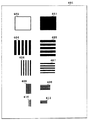
ここで、図4を参照して詳細に説明する。図4中で、401は画像データもしくは紙上に印字された全体を表し、402は白部の基準となる白パッチを、403は黒部の基準となる黒パッチを表す。
【0054】
404は、周波数2本/mmに相当する黒と白の繰り返しパターン、405は、404と同一パターンを90°回転したパターン、406は、周波数4本/mmに相当する黒と白の繰り返しパターン、407は、406と同一パターンを90°回転したパターン、408は、周波数6本/mmに相当する黒と白の繰り返しパターン、409は、408と同一パターンを90°回転したパターン、410は、周波数8本/mmに相当する黒と白の繰り返しパターン、411は、410と同一パターンを90°回転したパターンである。
【0055】
画像領域判定回路111は、図4におけるパッチおよびパターン402〜411が占める夫々の領域を切り出し、補正値算出回路112は、夫々の領域の読み取り値からフィルタ係数を算出する。以下の説明において、便宜上、上記切り出されるパターンの占有領域を「領域」と記し、該当パターンの参照符号で表す。
【0056】
先ず、領域402を読み取り、その平均値Wを求める。次に、領域403を読み取り、その平均値Bを求める。そして、領域404〜411については、図6に示すように、最大値と最小値を求める。
【0057】
即ち、領域404の最大値W1と最小値B1、領域405の最大値W2と最小値B2、領域406の最大値W3と最小値B3、領域407の最大値W4と最小値B4、領域408の最大値W5と最小値B5、領域409の最大値W6と最小値B6、領域410の最大値W7と最小値B7、および領域411の最大値W8と最小値B8を夫々求め、これらの値から、各パターンの該当周波数におけるMTFを求める。
【0058】
即ち、2本/mmの主走査MTF(M2)および副走査MTF(S2)を、式(1)および式(2)より求める。
【0059】
M2=(W1−B1)/(W−B) (1)
S2=(W2−B2)/(W−B) (2)
【0060】
以下同様に、4本/mm、6本/mm、8本/mmの主走査MTF(M4,M6,M8)および副走査MTF(S4,S6,S8)を、式(3)〜式(8)にしたがって求める。
【0061】
M4=(W3−B3)/(W−B) (3)
S4=(W4−B4)/(W−B) (4)
M6=(W5−B5)/(W−B) (5)
S6=(W6−B6)/(W−B) (6)
M8=(W7−B7)/(W−B) (7)
S8=(W8−B8)/(W−B) (8)
【0062】
図7は、このようにして算出した各周波数におけるMTF特性を表わす特性図である。算出されたこの特性は、図8に示す補正特性を利用して補正でき、これにより所望のフィルタ係数を算出することが出来る。図8の補正特性は図7の特性を逆フーリエ変換することにより得られ、これにより各周波数のMTF特性を100%に補正するものである。
【0063】
なお、補正すべきターゲットは各周波数とも100%である必要はない。原稿よりも先鋭さ(シャープネス)を強調するモード、原稿よりも平滑化気味に再現するモード等、所望のMTFをターゲットとして、そのターゲットにMTFを補正するようにフィルタ係数を作ることも可能である。
【0064】
また、予めいくつかのフィルタ係数を用意しておき、計算されたMTF値に基づいていずれかのフィルタ係数を選択するような構成とすることもできる。
【0065】
(第2実施形態)
図9は、本発明に係る第2実施形態を示すブロック図である。
【0066】
ここに示す第2実施形態では、図2の第1実施形態における補正値算出回路112に代えて、リーダMTFとプリンタMTFを分けて記憶する記憶装置を設け、補正値算出手段もMTF算出とフィルタ係数算出に分けて設けた構成を採用した。
【0067】
第1実施形態では、MTF特性をリーダ部とプリンタ部で分けて記憶していなかったために、原稿台に置かれた原稿をリーダで読み取る動作を伴う複写動作とホストコンピュータ(図示せず)から送られてきたデータを印字する印字動作とではMTF特性の劣化が異なってしまう。そこで本実施形態では、リーダのMTFとプリンタのMTFを別々に記憶しておき、各動作に合致したフィルタ係数を算出させるために図9の構成を採用したのである。
【0068】
なお、ホストコンピュータから送られてきた画像データはプリンタコントローラ(図示せず)により展開され、展開された画像信号に基づいて画像記録が行なわれる。
【0069】
図9において、901はMTF算出回路、902はリーダMTF記憶装置、903はプリンタMTF記憶装置、904はフィルタ係数算出回路である。
【0070】
先ず、本実施形態においてリーダMTFを算出する場合を説明する。本実施形態では、図4に示した画像データを精密印刷したテストチャートを用意する。
【0071】
このチャートは、印刷によるMTF劣化の無い理想的な精密印刷機で印刷されているものとする。このチャートを原稿台ガラス302上に乗せて、読み取りユニット303による走査を行なって入力センサ部101に画像を読み込む。
【0072】
入力された画像データは、入力補正回路102により入力系のシェーディング補正が施され、画像メモリ110に記憶される。画像メモリ110に一時的に蓄えられた画像は画像領域判定回路111に送られる。画像領域判定回路111は、この画像データから各周波数を表す部分の切り出しを行ない、以降、本実施形態に特徴的な独立したリーダMTFに係る処理が行なわれる。
【0073】
すなわち、MTF算出回路901は各周波数に該当するパターンのMTFを判定し、その結果をリーダMTF記憶装置902に送る。リーダMTF記憶装置902はリーダMTFの値を記憶する。
【0074】
次にプリンタMTFを算出する場合を説明する。
【0075】
第1実施形態と同じように、先ず、パターン発生回路109により、図4を参照して説明したテストパターンを発生する。このテストパターンはMTF(Modulation Transfer Function)特性を検出するためのパターンであり、セレクタ103により画像信号として入力され、前述した画像処理要素のいくつかを通り(不必要な処理はスルーとなる)、プリンタ部108に入力される。プリンタ部108は、この画像データに基づいて印字を行う。
【0076】
そしてパターンの印字が終了するとプリンタ200より排出された用紙を原稿台ガラス302上に乗せて、読み取りユニット303の走査により入力センサ部101に画像を読み込む。入力された画像データは、入力補正回路102により入力系のシェーディング補正が施され、画像メモリ110に記憶される。画像メモリ110に一時的に蓄えられた画像は画像領域判定回路111に送られる。
【0077】
画像領域判定回路111は、この画像データから各周波数を表す部分の切り出しを行ない、以降、本実施形態に特徴的な独立したプリンタMTFに係る処理が行なわれる。
【0078】
すなわち、MTF算出回路901は各周波数に該当するパターンのMTFを判定し、そのMTF特性からリーダMTF成分を除いたものを、即ち各周波数においてリーダMTFで除算したものをプリンタMTFとして、プリンタMTF記憶装置903に送る。プリンタMTF記憶装置903は、算出されたプリンタMTFを記憶する。
【0079】
フィルタ係数算出回路904は、上述のようにして記憶装置902および記憶装置903に記憶した2つのMTFからフィルタ係数を算出する。つまり、プリンタMTFデータを読み出してプリント時フィルタ係数を算出し、リーダMTFデータとプリンタMTFデータを読み出して複写時フィルタ係数を算出する。算出された、この2種類のフィルタ係数は、バックアップRAM113に記憶される。
【0080】
そして、実際の複写時もしくはプリント時には、動作にマッチしたフィルタ係数がバックアップRAM113から読み出され、フィルタ107は、このフィルタ係数に基づいてフィルタ処理を施す。フィルタ107によるMTFのデジタル的な補正によって、原稿をリーダで読み取る複写動作とホストコンピュータ(図示せず)からのデータを印字する印字動作とでMTF特性を合致させた、プロセス条件の変化や固体差によるMTF劣化を良好に補正した高品位な画像を得ることができる。
【0081】
(第3実施形態)
図10は、本発明に係る第3実施形態を示すブロック図である。
【0082】
ここに示す第3実施形態では、図9の第2実施形態における画像メモリ110に代えて、パターン発生回路1009に接続したネットワークI/F1010を設けた構成を採用した。ネットワークI/F1010はネットワークケーブル1015に繋がっており、このネットワークケーブル1015に接続されている他の装置との通信を可能とする。
【0083】
例えば、本実施形態の記録装置と離れた場所にあるMFP(Multi Function Printer)1014と、ネットワークケーブル1015を介して通信する場合について考える。本実施形態装置の原稿読取装置300で読み込んだ画像を2値化してMFP1014に送信し、この画像をMFP1014によってプリントする、所謂ネットワークプリンティングを行なうに際しては、プリント実行前にネットワーク上で以下の補正動作を行わせる。なお、MFP1014はスキャナ部とプリンタ部を備えた多機能複写機であるが、MTF補正機能は備えていないものとする。
【0084】
先ず、パターン発生回路1009によって図4に示したようなパターンを発生させる。そして、ネットワークI/F1010は、そのパターンをパターン発生回路1009から受け取って、ネットワークケーブル1015を通じてMFP1014に送信する。MFP1014は、そのパターンを紙等にプリント出力する。
【0085】
次に、このようにしてMFP1014により出力されたパターン、または第2実施形態で用いた精密印刷されたチャートをMFP1014のスキャナ部で読み取り、その画像読取データをMFP1014からネットワークI/F1010へ、ネットワークケーブル1015を通じて送信する。
【0086】
そして、本実施形態装置側で、MFP1014から送られてきた画像データに基づいて第2実施形態と同一のアルゴリズムを用いてフィルタ係数の補正を行うことにより、ネットワークを通じてMTF補正機能の無いMFP1014によりプリントする場合、或いはMFP1014によりスキャンさせて画像を取り込む場合においても、夫々のリーダMTF、プリンタMTFからフィルタ係数を算出し、フィルタ処理を施すことにより、プロセス条件の変化や固体差によるMTF劣化を良好に補正した良好な画像をネットワーク上で得ることが出来る。
【0087】
(他の実施形態)
上記実施形態の他に、第1実施形態と第3実施形態を組み合わせた構成、つまり、第1実施形態における画像メモリに代えてパターン発生回路に接続したネットワークI/Fを設けた構成を実施することもできる。
【0088】
【発明の効果】
以上説明したように本発明に係る記録装置によれば、読み取り手段及び記録手段のMTF特性を判定し、それらを組み合わせてフィルタ係数を算出し、この係数を用いてデジタルフィルタによるフィルタ処理を施すことにより、記録手段のプロセス条件の変化や固体差によるMTF劣化を良好に補正することが出来、また、ネットワークを介してつながっている他の記録装置等に対しても、それぞれの特性に応じたMTF補正、すなわち、個体差を考慮した補正を行うことが出来るため、記録品位を向上させることが可能となる。
【図面の簡単な説明】
【図1】本発明に係る第1実施形態の記録装置を示した内部構成図である。
【図2】本発明に係る第1実施形態の記録装置を示したブロック図である。
【図3】フィルタ係数の詳細を示した説明図である。
【図4】MTF判定用のパターンデータ及び印刷されたチャートの詳細を表す平面図である。
【図5】デジタルフィルタのハードウエア構成図である。
【図6】読み取ったデータの最大値、最小値を説明する説明図である。
【図7】各周波数におけるMTF特性を示した特性図である。
【図8】MTF特性を補正するための特性を示した特性図である。
【図9】本発明に係る第2実施形態の記録装置を示したブロック図である。
【図10】本発明に係る第3実施形態の記録装置を示したブロック図である。
【符号の説明】
101 入力センサ部
102 入力補正回路
103 セレクタ
107 フィルタ
108 プリンタ部
109 パターン発生回路
110 画像メモリ
111 画像領域判定回路
112 補正値算出回路
113,114 バックアップRAM
200 プリンタ
201 カセット
202 ピックアップローラ
203,205 レジローラ
204 ガイド板
206 搬送ベルト
207 プラテン
208 定着器
209 排紙ガイド
210 排紙ローラ
211 排紙トレイ
212a アレイ
213a 現像器
214a ドラム
300 原稿読取装置
301 原稿圧板
302 原稿台ガラス
303 ユニット
304 拡散板
305,308,309 ミラー
306 照明ランプ
307 ミラーユニット
310 レンズ
501,516 遅延器
505,520 乗算器
510 加算器
515 ラインメモリ
901 算出回路
902,903 記憶装置
904 フィルタ係数算出回路
1009 パターン発生回路
1010 ネットワークI/F
1015 ネットワークケーブル[0001]
BACKGROUND OF THE INVENTION
The present invention relates to a recording apparatus, and more particularly, a recording apparatus that includes a digital filter and corrects MTF degradation by image input / output, and corrects MTF degradation by image input / output between recording apparatuses connected to a network. The present invention relates to a recording apparatus.
[0002]
[Prior art]
As this type of apparatus, an electrophotographic recording apparatus is generally known.
[0003]
In such a recording apparatus, the reading unit is provided with a photoelectric conversion element such as a CCD, for example, and the image on the document is converted into an electrical signal by scanning the photoelectric conversion element relative to the document. Then, a latent image is formed on the photosensitive drum by driving a laser light source or an LED based on the electric signal obtained by the reading. A toner is attached to a portion where a potential difference is generated by the latent image and developed, and the visualized image is transferred onto a recording medium such as a recording paper and reproduced.
[0004]
[Problems to be solved by the invention]
In such an electrophotographic recording apparatus, process conditions may change due to environmental conditions, changes with time, material deterioration, and the like. Due to such a change in process conditions, there arises a problem that the MTF (Modulation Transfer Function) of the image deteriorates when the read image is reproduced on paper. This deterioration varies depending on the electrophotographic apparatus, and may change with time.
[0005]
Further, when printing or scanning via a network, there is a problem that a good image cannot be obtained if data is exchanged between devices having different MTF characteristics.
[0006]
The present invention has been made on the basis of the above-mentioned viewpoint, and the object is to set an optimum filter coefficient and perform good MTF correction to improve the recording quality even when the MTF characteristic changes. It is an object of the present invention to provide a recording apparatus that can perform the above-described operation.
[0007]
[Means for Solving the Problems]
One aspect of the present invention made to solve the above problems is a recording apparatus connected to another recording apparatus via a network, wherein the image reading means Or host device An image processing means for performing predetermined image processing on the image signal obtained by the above, a recording means for recording an image corresponding to the image signal processed by the image processing means on a recording material, and a test pattern including a plurality of types of patterns Test pattern generating means for generating a test pattern corresponding to an image signal having a different frequency for each pattern, and means for transmitting and receiving image signals to and from the other recording apparatus having other image reading means and other recording means The test pattern is transmitted to the other recording device, and the other image reading means is A read signal obtained by reading a test chart on which a predetermined pattern is printed Communication means for receiving a read signal obtained by reading the test pattern printed on the recording material using the other recording means, and the other based on the received signal Record means Frequency characteristics And the other Image reading The frequency characteristics of the means Independently Detecting means for detecting, and by the detecting means R detection From the respective frequency characteristics of the other recording means and the other image reading means Calculating means for calculating a filter coefficient used in the digital filter means included in the image processing means, When recording by other recording means and when reading by the other image reading means, the calculated filter coefficient is used. Said each A band pass characteristic filtering process is performed to correct the frequency characteristic.
[0009]
the above State of The test pattern generation means generates a plurality of repetitive patterns having different repetition frequencies in the main scanning direction of the image reading means and a plurality of repetitive patterns having different repetition frequencies in the sub-scanning direction of the image reading means. Can do. In the latter embodiment, the test chart is other A plurality of repetitive patterns having different repetitive frequencies in the main scanning direction of the image reading means; other A plurality of repetitive patterns having different repetitive frequencies in the sub-scanning direction of the image reading means may be printed in advance.
[0011]
The present invention Another Is a recording apparatus connected to another recording apparatus via a network, the image processing means for performing predetermined image processing on the image signal obtained by the image reading means or the host device, and the image processing means A test chart in which a recording unit for recording an image corresponding to the processed image signal on a recording material and another image reading unit provided in the other recording apparatus are printed with a predetermined pattern in advance. Read signal read And receiving means for receiving a read signal obtained by reading a test pattern printed on a recording material using other recording means provided in the recording apparatus, and the other based on the received signal. Record means Frequency characteristics And the other Image reading Detecting means for independently detecting the frequency characteristics of the means; and R detection From the respective frequency characteristics of the other recording means and the other image reading means Calculating means for calculating a filter coefficient used in the digital filter means included in the image processing means, When recording by other recording means and when reading by the other image reading means, the calculated filter coefficient is used. Said each A band pass characteristic filtering process is performed to correct the frequency characteristic.
[0021]
DETAILED DESCRIPTION OF THE INVENTION
(First embodiment)
Hereinafter, embodiments of the present invention will be described in detail with reference to the drawings.
[0022]
FIG. 1 is an internal configuration diagram of a recording apparatus capable of image copying showing a first embodiment according to the present invention.
[0023]
The
[0024]
The
[0025]
Next, the image signal is subjected to image processing described later, and then sent to the
[0026]
In the
[0027]
On the other hand, the image signal is separated into four colors CMYK. Among them, the C (cyan) signal is converted into an optical signal by the
[0028]
Similarly, the remaining M (magenta), Y (yellow), and K (black) are similarly image-formed by a well-known electrophotographic process using a set of LED array, drum, and developer, and the toner image is transferred to the paper. The The toner transferred onto the paper is heated and fixed on the paper by the
[0029]
FIG. 2 is a block diagram showing a first embodiment according to the present invention.
[0030]
In FIG. 2, an input sensor unit 101 includes a photoelectric conversion element such as a CCD and a driving device that moves the photoelectric conversion element for scanning, thereby reading and scanning a document. Document image data read by the input sensor unit 101 is sequentially sent to the input correction circuit 102. Here, quantization for converting each pixel image data into digital data is performed, and shading correction for correcting unevenness in sensitivity of the CCD sensor and unevenness in illuminance by the illumination light source is performed by digital arithmetic processing.
[0031]
The
[0032]
[0033]
An
[0034]
A case where filter coefficients are calculated in the above configuration will be described.
[0035]
First, the
[0036]
When the pattern printing is completed, the paper discharged from the
[0037]
The image
[0038]
Then, during normal image copying, the MTF of the image is digitally corrected by the
[0039]
Next, details of the digital filter will be described.
[0040]
This digital filter is configured in two dimensions, and in the present embodiment, a 5 × 5 size filter will be described as an example. The filter size is not limited to 5 × 5, and may be 9 × 9, 7 × 7, or the like. Of course, it may be larger than that, or may have a different size (for example, 9 × 7) in the main scanning direction and the sub-scanning direction.
[0041]
FIG. 3 shows a functional configuration of the digital filter.
[0042]
FIG. 3 shows how the coefficients of the digital filter are entered. The digital filter shown here performs a convolution operation of 25 pixels including the pixel of interest (i, j).
[0043]
When each coefficient is represented by An, m and the value of each pixel is S (i, j), the output result F (i, j) subjected to the filter operation is represented by the following expression.
[0044]
[Expression 1]
FIG. 5 shows the hardware configuration of the digital filter.
[0046]
In FIG. 5,
[0047]
In the above configuration, the input image data is sequentially delayed pixel by pixel by the
[0048]
The
[0049]
[0050]
As described above, the result of multiplying all the 25 pixels by the coefficients by the
[0051]
Details of the correction value calculation will be described below.
[0052]
The image data stored in the
[0053]
Here, it demonstrates in detail with reference to FIG. In FIG. 4, 401 represents image data or the whole printed on paper, 402 represents a white patch serving as a reference for white portions, and 403 represents a black patch serving as a reference for black portions.
[0054]
404 is a black and white repetitive pattern corresponding to a frequency of 2 lines / mm, 405 is a pattern obtained by rotating the same pattern as that of 90 ° by 90 °, 406 is a black and white repetitive pattern corresponding to a frequency of 4 lines / mm, 407 is a pattern obtained by rotating the same pattern as 406 by 90 °, 408 is a black and white repeating pattern corresponding to a frequency of 6 lines / mm, 409 is a pattern obtained by rotating the same pattern as 408 by 90 °, and 410 is a frequency. A black and white repetitive pattern corresponding to 8 lines / mm, 411 is a pattern obtained by rotating the same pattern as 410 by 90 °.
[0055]
The image
[0056]
First, the
[0057]
That is, the maximum value W1 and minimum value B1 of the
[0058]
That is, the main scanning MTF (M2) and the sub-scanning MTF (S2) of 2 lines / mm are obtained from the equations (1) and (2).
[0059]
M2 = (W1-B1) / (WB) (1)
S2 = (W2-B2) / (W-B) (2)
[0060]
Similarly, the main scanning MTFs (M4, M6, M8) and the sub-scanning MTFs (S4, S6, S8) of 4 lines / mm, 6 lines / mm, and 8 lines / mm are expressed by equations (3) to (8). )
[0061]
M4 = (W3-B3) / (W-B) (3)
S4 = (W4-B4) / (W-B) (4)
M6 = (W5-B5) / (W-B) (5)
S6 = (W6-B6) / (W-B) (6)
M8 = (W7−B7) / (W−B) (7)
S8 = (W8−B8) / (W−B) (8)
[0062]
FIG. 7 is a characteristic diagram showing the MTF characteristic at each frequency calculated as described above. This calculated characteristic can be corrected by using the correction characteristic shown in FIG. 8, and thereby a desired filter coefficient can be calculated. The correction characteristic shown in FIG. 8 is obtained by performing inverse Fourier transform on the characteristic shown in FIG. 7, thereby correcting the MTF characteristic of each frequency to 100%.
[0063]
Note that the target to be corrected need not be 100% for each frequency. It is also possible to create a filter coefficient so that the target MTF is targeted and the target MTF is corrected, such as a mode that emphasizes sharpness (sharpness) than the original and a mode that reproduces more smoothly than the original. .
[0064]
Alternatively, a configuration may be adopted in which some filter coefficients are prepared in advance and any one of the filter coefficients is selected based on the calculated MTF value.
[0065]
(Second Embodiment)
FIG. 9 is a block diagram showing a second embodiment according to the present invention.
[0066]
In the second embodiment shown here, in place of the correction
[0067]
In the first embodiment, since the MTF characteristics are not separately stored in the reader unit and the printer unit, the copying operation involving the operation of reading the document placed on the document table by the reader and the transmission from the host computer (not shown). Deterioration of the MTF characteristics is different from the printing operation for printing the received data. Therefore, in the present embodiment, the configuration shown in FIG. 9 is adopted in order to store the MTF of the reader and the MTF of the printer separately and calculate the filter coefficients that match each operation.
[0068]
Image data sent from the host computer is developed by a printer controller (not shown), and image recording is performed based on the developed image signal.
[0069]
In FIG. 9,
[0070]
First, a case where the reader MTF is calculated in the present embodiment will be described. In this embodiment, a test chart is prepared by precisely printing the image data shown in FIG.
[0071]
It is assumed that this chart is printed by an ideal precision printing machine with no MTF deterioration due to printing. This chart is placed on the
[0072]
The input image data is subjected to input shading correction by the input correction circuit 102 and stored in the
[0073]
That is, the
[0074]
Next, a case where the printer MTF is calculated will be described.
[0075]
As in the first embodiment, first, the
[0076]
When the pattern printing is completed, the paper discharged from the
[0077]
The image
[0078]
That is, the
[0079]
The filter coefficient calculation circuit 904 calculates a filter coefficient from the two MTFs stored in the
[0080]
Then, at the time of actual copying or printing, the filter coefficient matching the operation is read from the
[0081]
(Third embodiment)
FIG. 10 is a block diagram showing a third embodiment according to the present invention.
[0082]
In the third embodiment shown here, a configuration in which a network I /
[0083]
For example, consider a case where communication is performed via a
[0084]
First, the pattern generation circuit 1009 generates a pattern as shown in FIG. The network I /
[0085]
Next, the pattern output by the
[0086]
Then, the apparatus according to the present exemplary embodiment performs the correction of the filter coefficient using the same algorithm as that of the second exemplary embodiment on the basis of the image data transmitted from the
[0087]
(Other embodiments)
In addition to the above-described embodiment, a configuration in which the first embodiment and the third embodiment are combined, that is, a configuration in which a network I / F connected to the pattern generation circuit is provided instead of the image memory in the first embodiment is implemented. You can also.
[0088]
【The invention's effect】
As described above, according to the recording apparatus of the present invention, the MTF characteristics of the reading unit and the recording unit are determined, a filter coefficient is calculated by combining them, and a filter process using a digital filter is performed using this coefficient. Therefore, it is possible to satisfactorily correct MTF degradation due to changes in the process conditions of the recording means and individual differences, and also to other recording devices connected via a network, the MTF corresponding to each characteristic. Since the correction, that is, the correction considering individual differences can be performed, the recording quality can be improved.
[Brief description of the drawings]
FIG. 1 is an internal configuration diagram illustrating a recording apparatus according to a first embodiment of the invention.
FIG. 2 is a block diagram showing the recording apparatus of the first embodiment according to the present invention.
FIG. 3 is an explanatory diagram showing details of filter coefficients.
FIG. 4 is a plan view showing details of pattern data for MTF determination and a printed chart.
FIG. 5 is a hardware configuration diagram of a digital filter.
FIG. 6 is an explanatory diagram for explaining a maximum value and a minimum value of read data.
FIG. 7 is a characteristic diagram showing MTF characteristics at each frequency.
FIG. 8 is a characteristic diagram showing characteristics for correcting MTF characteristics.
FIG. 9 is a block diagram illustrating a recording apparatus according to a second embodiment of the invention.
FIG. 10 is a block diagram illustrating a recording apparatus according to a third embodiment of the invention.
[Explanation of symbols]
101 Input sensor section
102 Input correction circuit
103 selector
107 Filter
108 Printer
109 Pattern generation circuit
110 Image memory
111 Image Area Determination Circuit
112 Correction value calculation circuit
113,114 Backup RAM
200 printer
201 cassette
202 Pickup roller
203, 205 cashier roller
204 Guide plate
206 Conveyor belt
207 Platen
208 Fixer
209 Paper ejection guide
210 Paper discharge roller
211 Output tray
212a array
213a Developer
214a drum
300 Document reader
301 Document platen
302 Platen glass
303 units
304 Diffuser
305, 308, 309 mirror
306 Lighting lamp
307 mirror unit
310 lens
501 and 516 delay units
505, 520 multiplier
510 adder
515 line memory
901 Calculation circuit
902, 903 storage device
904 Filter coefficient calculation circuit
1009 Pattern generation circuit
1010 Network I / F
1015 Network cable
Claims (4)
画像読み取り手段またはホスト装置により得た画像信号に所定の画像処理を行う画像処理手段と、
該画像処理手段により処理された画像信号に応じた画像を被記録材に記録する記録手段と、
複数種類のパターンを含むテストパターンであって各パターンが異なる周波数の画像信号に対応するテストパターンを発生するテストパターン発生手段と、
他の画像読み取り手段および他の記録手段を有する前記他の記録装置と画像信号の送受信を行なう手段であって、前記テストパターンを前記他の記録装置に送信し、前記他の画像読み取り手段が、予め所定パターンがプリントされたテストチャートを読み取った読み取り信号および前記他の記録手段を用いて被記録材にプリントされた前記テストパターンを読み取った読み取り信号を受信する通信手段と、
受信した信号に基づき前記他の記録手段の周波数特性および前記他の画像読み取り手段の周波数特性を独立して検出する検出手段と、
該検出手段により検出した前記他の記録手段および前記他の画像読み取り手段の各周波数特性から、前記画像処理手段が有するデジタルフィルタ手段に用いられるフィルタ係数を算出する算出手段とを備え、
前記他の記録手段により記録する場合、および、前記他の画像読み取り手段により読み取る場合に、該算出したフィルタ係数を用いて前記各周波数特性を補正するような帯域通過特性のフィルタ処理を行なう
ことを特徴とする記録装置。A recording device connected to another recording device via a network,
Image processing means for performing predetermined image processing on an image signal obtained by an image reading means or a host device;
Recording means for recording an image corresponding to the image signal processed by the image processing means on a recording material;
Test pattern generating means for generating a test pattern corresponding to an image signal having a different frequency, which is a test pattern including a plurality of types of patterns,
A means for transmitting and receiving an image signal to and from the other recording apparatus having other image reading means and other recording means, wherein the test pattern is transmitted to the other recording apparatus, and the other image reading means communication means for receiving a read signal obtained by reading said test pattern is printed on a recording medium by using a read signal and the other recording means by reading a pre-test chart on which a predetermined pattern is printed,
Detecting means for independently detecting the frequency characteristics of the other recording means and the frequency characteristics of the other image reading means based on the received signal;
From each frequency characteristic of the detection the other recording means and said other image reading means detected Ri by the unit, and a calculating means for calculating the filter coefficients used in the digital filter means having said image processing means,
When recording by the other recording means and when reading by the other image reading means , the filter processing of the band pass characteristic is performed so as to correct each frequency characteristic using the calculated filter coefficient. A recording apparatus.
前記テストパターン発生手段は、前記画像読み取り手段の主走査方向に繰り返し周波数が異なる複数の繰り返しパターンと、前記画像読み取り手段の副走査方向に繰り返し周波数が異なる複数の繰り返しパターンを発生させることを特徴とする記録装置。The recording apparatus according to claim 1,
The test pattern generation means generates a plurality of repetitive patterns having different repetition frequencies in the main scanning direction of the image reading means and a plurality of repetitive patterns having different repetition frequencies in the sub-scanning direction of the image reading means. Recording device.
前記テストチャートは、前記他の画像読み取り手段の主走査方向に繰り返し周波数が異なる複数の繰り返しパターンと、前記他の画像読み取り手段の副走査方向に繰り返し周波数が異なる複数の繰り返しパターンを予めプリントされていることを特徴とする記録装置。The recording apparatus according to claim 1,
The test chart, and the other image reading means in the main scanning direction is repeated a plurality of repetitive patterns of different frequencies, a plurality of repetitive patterns repetition frequency in the sub-scanning direction different from the other image reading means is preprinted A recording apparatus.
画像読み取り手段またはホスト装置により得た画像信号に所定の画像処理を行う画像処理手段と、
該画像処理手段により処理された画像信号に応じた画像を被記録材に記録する記録手段と、
前記他の記録装置に備えられた他の画像読み取り手段が、予め所定パターンがプリントされたテストチャートを読み取った読み取り信号および該記録装置に備えられた他の記録手段を用いて被記録材にプリントされたテストパターンを読み取った読み取り信号を受信する受信手段と、
受信した信号に基づき前記他の記録手段の周波数特性および前記他の画像読み取り手段の周波数特性を独立して検出する検出手段と、
該検出手段により検出した前記他の記録手段および前記他の画像読み取り手段の各周波数特性から、前記画像処理手段が有するデジタルフィルタ手段に用いられるフィルタ係数を算出する算出手段とを備え、
前記他の記録手段により記録する場合、および、前記他の画像読み取り手段により読み取る場合に、該算出したフィルタ係数を用いて前記各周波数特性を補正するような帯域通過特性のフィルタ処理を行なう
ことを特徴とする記録装置。A recording device connected to another recording device via a network,
Image processing means for performing predetermined image processing on an image signal obtained by an image reading means or a host device;
Recording means for recording an image corresponding to the image signal processed by the image processing means on a recording material;
Other image reading means provided in the other recording apparatus prints on a recording material using a read signal obtained by reading a test chart on which a predetermined pattern is printed in advance and the other recording means provided in the recording apparatus. Receiving means for receiving a read signal obtained by reading the test pattern,
Detecting means for independently detecting the frequency characteristics of the other recording means and the frequency characteristics of the other image reading means based on the received signal;
From each frequency characteristic of the detection the other recording means and said other image reading means detected Ri by the unit, and a calculating means for calculating the filter coefficients used in the digital filter means having said image processing means,
When recording by the other recording means and when reading by the other image reading means , the filter processing of the band pass characteristic is performed so as to correct each frequency characteristic using the calculated filter coefficient. A recording apparatus.
Priority Applications (1)
| Application Number | Priority Date | Filing Date | Title |
|---|---|---|---|
| JP2000399276A JP4401567B2 (en) | 2000-12-27 | 2000-12-27 | Recording device |
Applications Claiming Priority (1)
| Application Number | Priority Date | Filing Date | Title |
|---|---|---|---|
| JP2000399276A JP4401567B2 (en) | 2000-12-27 | 2000-12-27 | Recording device |
Publications (3)
| Publication Number | Publication Date |
|---|---|
| JP2002199224A JP2002199224A (en) | 2002-07-12 |
| JP2002199224A5 JP2002199224A5 (en) | 2008-02-14 |
| JP4401567B2 true JP4401567B2 (en) | 2010-01-20 |
Family
ID=18864075
Family Applications (1)
| Application Number | Title | Priority Date | Filing Date |
|---|---|---|---|
| JP2000399276A Expired - Fee Related JP4401567B2 (en) | 2000-12-27 | 2000-12-27 | Recording device |
Country Status (1)
| Country | Link |
|---|---|
| JP (1) | JP4401567B2 (en) |
Families Citing this family (2)
| Publication number | Priority date | Publication date | Assignee | Title |
|---|---|---|---|---|
| JP4595771B2 (en) * | 2005-09-28 | 2010-12-08 | セイコーエプソン株式会社 | Color conversion device |
| EP2206334A2 (en) * | 2007-09-28 | 2010-07-14 | OCE-Technologies B.V. | Method, apparatus and computer program for adaptive compensation of a mtf |
-
2000
- 2000-12-27 JP JP2000399276A patent/JP4401567B2/en not_active Expired - Fee Related
Also Published As
| Publication number | Publication date |
|---|---|
| JP2002199224A (en) | 2002-07-12 |
Similar Documents
| Publication | Publication Date | Title |
|---|---|---|
| US8270046B2 (en) | Image processor and image processing method for extracting removal color and color around removal color in an image prior to image color/monochrome determination | |
| EP1265434A1 (en) | Image processing method and apparatus and image processing system | |
| JP2008271488A (en) | Image processing method, image processing apparatus, image forming apparatus, image reading apparatus, computer program, and recording medium | |
| US6603566B1 (en) | Image forming apparatus, image processing method, and recording medium | |
| US7110128B1 (en) | Controlling dot connectivity in binarizing an image | |
| JP4401567B2 (en) | Recording device | |
| JP2003341186A (en) | Imaging apparatus | |
| JP3884890B2 (en) | Image processing apparatus and method | |
| JP3723043B2 (en) | Image processing apparatus, image reading apparatus, and image forming apparatus | |
| JPH0851536A (en) | Image processing method and device therefor | |
| JP2007088561A (en) | Image processor and processing method | |
| US6002841A (en) | Apparatus and method for processing image which adds identification information to be easily decipherable in high resolution image | |
| US7375853B2 (en) | Image processing apparatus and method | |
| JPH0477060A (en) | Image forming device | |
| JP3688100B2 (en) | Image processing device | |
| JP3447275B2 (en) | Image processing method and apparatus | |
| JP2001045306A (en) | Method and device for forming image | |
| JPH11266366A (en) | Image copying machine | |
| JP3281391B2 (en) | Full-color image reproducing apparatus and full-color image reproducing method | |
| JP3191300B2 (en) | Full-color image processing device | |
| JP2004357144A (en) | Information reader | |
| JP2003162382A (en) | Device for forming color image and color copying device | |
| JP2005176222A (en) | Image processor | |
| JP3794807B2 (en) | Color image processing device | |
| JP2000022895A (en) | Image processor, image processing method and storage medium |
Legal Events
| Date | Code | Title | Description |
|---|---|---|---|
| A521 | Written amendment |
Free format text: JAPANESE INTERMEDIATE CODE: A523 Effective date: 20071226 |
|
| A621 | Written request for application examination |
Free format text: JAPANESE INTERMEDIATE CODE: A621 Effective date: 20071226 |
|
| A977 | Report on retrieval |
Free format text: JAPANESE INTERMEDIATE CODE: A971007 Effective date: 20090312 |
|
| A131 | Notification of reasons for refusal |
Free format text: JAPANESE INTERMEDIATE CODE: A131 Effective date: 20090317 |
|
| A521 | Written amendment |
Free format text: JAPANESE INTERMEDIATE CODE: A523 Effective date: 20090518 |
|
| A131 | Notification of reasons for refusal |
Free format text: JAPANESE INTERMEDIATE CODE: A131 Effective date: 20090623 |
|
| A521 | Written amendment |
Free format text: JAPANESE INTERMEDIATE CODE: A523 Effective date: 20090824 |
|
| TRDD | Decision of grant or rejection written | ||
| A01 | Written decision to grant a patent or to grant a registration (utility model) |
Free format text: JAPANESE INTERMEDIATE CODE: A01 Effective date: 20091016 |
|
| A01 | Written decision to grant a patent or to grant a registration (utility model) |
Free format text: JAPANESE INTERMEDIATE CODE: A01 |
|
| A61 | First payment of annual fees (during grant procedure) |
Free format text: JAPANESE INTERMEDIATE CODE: A61 Effective date: 20091028 |
|
| R150 | Certificate of patent or registration of utility model |
Free format text: JAPANESE INTERMEDIATE CODE: R150 |
|
| FPAY | Renewal fee payment (event date is renewal date of database) |
Free format text: PAYMENT UNTIL: 20121106 Year of fee payment: 3 |
|
| FPAY | Renewal fee payment (event date is renewal date of database) |
Free format text: PAYMENT UNTIL: 20131106 Year of fee payment: 4 |
|
| LAPS | Cancellation because of no payment of annual fees |